AC/DC Convertor IC PWM Type DC/DC converter IC ... -...
23
Datasheet ○Product structure:Silicon monolithic integrated circuit ○This product has no designed protection against radioactive rays. . 1/20 TSZ02201-0F1F0A200100-1-2 22. Mar.2017.Rev.002 © 2015 ROHM Co., Ltd. All rights reserved. TSZ22111・14・001 www.rohm.com AC/DC Convertor IC PWM Type DC/DC converter IC Integrated Switching MOSFET BM2PXXA/BM2PXXB Series General Description The PWM Type DC/DC converter for AC/DC provides an optimal system for all products that include an electrical outlet. BM2PXXA/BM2PXXB supports both isolated and non-isolated devices, enabling simpler design of various Types of high-efficiency electrical converters. The built-in starter circuit which withstand 650V pressure contributes to low-power consumption. Design can be easily implemented because includes a sensing resistor. Current is restricted in each cycle and excellent performance is demonstrated in bandwidth and transient response since current mode control is utilized. The switching frequency is 100 kHz. At light load, the switching frequency is reduced and high efficiency is achieved. A frequency hopping function that contributes to low EMI is also included on chip. Design can be easily implemented because includes a 650V switching Super Junction MOSFET. Key Features ■PWM frequency : 100kHz ■PWM current mode control ■Frequency hopping function ■Burst operation when load is light ■Frequency reduction function ■Built-in 650V starter circuit ■Built-in 650V switching MOSFET ■VCC pin Under-Voltage protection ■VCC pin Over-Voltage protection ■Per-cycle Over-Current Protection Circuit ■AC Correction function of Over current limiter ■Soft start ■Secondary Over-Current Protection Circuit ■External LATCH function ■X-Capacitor discharge function Applications For AC adapters and household appliances Basic specifications ■Operating Power Supply Voltage Range VCC :10.9V to 26.0V DRAIN :to 650V VH :to 650V ■Normal Operating Current :1.40mA (Typ.) ■Burst Operating Current :0.25mA (Typ.) ■Oscillation Frequency :100kHz (Typ.) ■Operating Temperature :- 40 o C to +105 o C ■MOSFET ON Resistance :2.0Ω (Typ.) Package DIP8 9.27mm×6.35mm×5.33mm pitch 2.54mm (Typ.) (Typ.) (Max.) Line-up Current Limitter VCCOVP FBOLP BM2P01A 0.43A Latch Latch BM2P11A 0.43A Latch Auto Restart BM2P21A 0.43A Auto Restart Latch BM2P31A 0.43A Auto Restart Auto Restart BM2P01B 0.54A Latch Latch BM2P11B 0.54A Latch Auto Restart BM2P21B 0.54A Auto Restart Latch BM2P31B 0.54A Auto Restart Auto Restart Application Circuit AC Input FUSE Filter Diode Bridge ERROR AMP 5 7 FB GND VCC VH 8 1 DRAIN 2 3 4 DRAIN LATCH 6 DRAIN
Transcript of AC/DC Convertor IC PWM Type DC/DC converter IC ... -...
Datasheet
Product structure:Silicon monolithic integrated circuit This product has no designed protection against radioactive rays. .
1/20
TSZ02201-0F1F0A200100-1-222. Mar.2017.Rev.002
© 2015 ROHM Co., Ltd. All rights reserved. TSZ22111・14・001
www.rohm.com
AC/DC Convertor IC
PWM Type DC/DC converter IC Integrated Switching MOSFET BM2PXXA/BM2PXXB Series
General Description The PWM Type DC/DC converter for AC/DC provides an optimal system for all products that include an electrical outlet. BM2PXXA/BM2PXXB supports both isolated and non-isolated devices, enabling simpler design of various Types of high-efficiency electrical converters. The built-in starter circuit which withstand 650V pressure contributes to low-power consumption. Design can be easily implemented because includes a sensing resistor. Current is restricted in each cycle and excellent performance is demonstrated in bandwidth and transient response since current mode control is utilized. The switching frequency is 100 kHz. At light load, the switching frequency is reduced and high efficiency is achieved. A frequency hopping function that contributes to low EMI is also included on chip. Design can be easily implemented because includes a 650V switching Super Junction MOSFET.
Key Features PWM frequency : 100kHz PWM current mode control Frequency hopping function Burst operation when load is light Frequency reduction function Built-in 650V starter circuit Built-in 650V switching MOSFET VCC pin Under-Voltage protection VCC pin Over-Voltage protection Per-cycle Over-Current Protection Circuit AC Correction function of Over current limiter Soft start Secondary Over-Current Protection Circuit External LATCH function X-Capacitor discharge function
Applications For AC adapters and household appliances
Basic specifications Operating Power Supply Voltage Range
VCC :10.9V to 26.0V DRAIN :to 650V VH :to 650V Normal Operating Current :1.40mA (Typ.) Burst Operating Current :0.25mA (Typ.) Oscillation Frequency :100kHz (Typ.) Operating Temperature :- 40 oC to +105 oC MOSFET ON Resistance :2.0Ω (Typ.)
Package DIP8 9.27mm×6.35mm×5.33mm pitch 2.54mm
(Typ.) (Typ.) (Max.)
Line-up
Current Limitter VCCOVP FBOLP
BM2P01A 0.43A Latch Latch
BM2P11A 0.43A Latch Auto Restart
BM2P21A 0.43A Auto Restart Latch
BM2P31A 0.43A Auto Restart Auto Restart
BM2P01B 0.54A Latch Latch
BM2P11B 0.54A Latch Auto Restart
BM2P21B 0.54A Auto Restart Latch
BM2P31B 0.54A Auto Restart Auto Restart
Application Circuit AC
Input
FUSE
FilterDiodeBridge
ERRORAMP
57
FBGND VCC
VH
8
1
DRAIN
2 3 4
DRAIN
LATCH
6
DRAIN
2/20
DatasheetDatasheetBM2PX1A/BM2PX1B Series
TSZ02201-0F1F0A200100-1-222. Mar.2017.Rev.002
© 2015 ROHM Co., Ltd. All rights reserved. www.rohm.com
TSZ22111・15・001
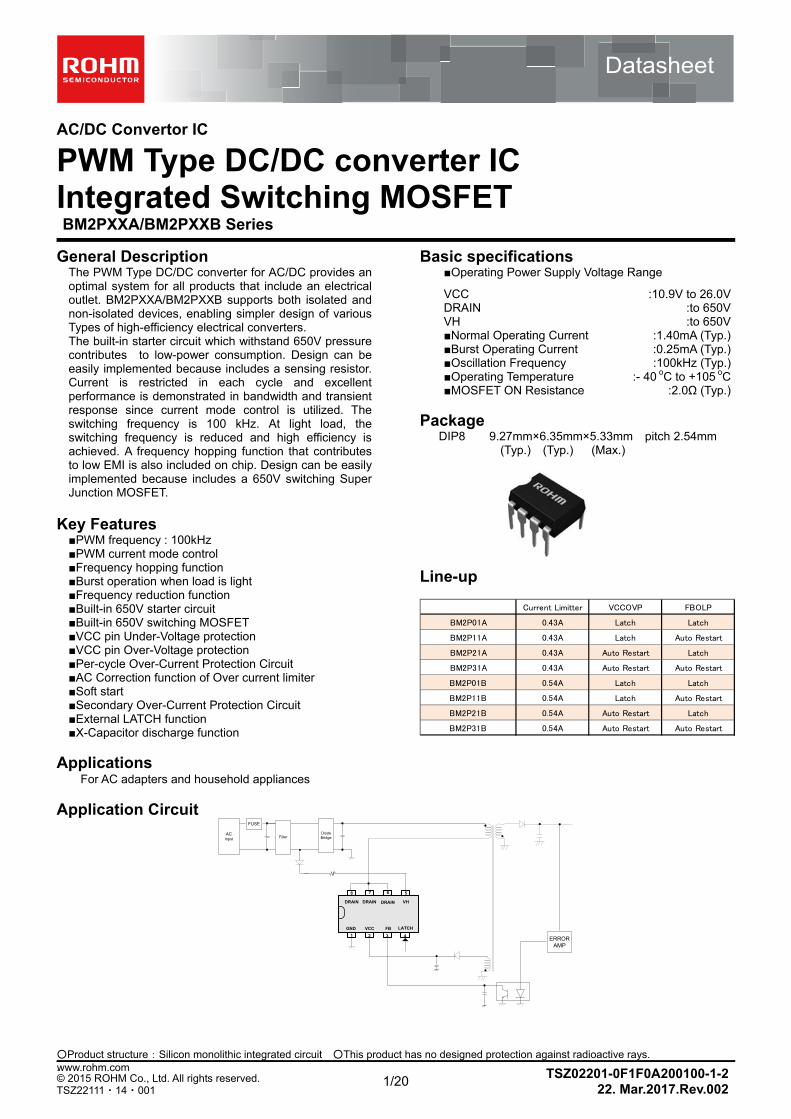
Pin Descriptions
NO. Pin Name I/O Function ESD Diode
VCC GND
1 GND I/O GND pin -
2 VCC I Power Supply pin -
3 FB I Feedback pin
4 LATCH I External Latch
5 VH I Start up pin -
6 DRAIN I/O MOSFET DRAIN pin - -
7 DRAIN I/O MOSFET DRAIN pin - -
8 DRAIN I/O MOSFET DRAIN pin - -
Block Diagram
0.18V/0.15V(FB=0.23V/0.18V)
PWM Control
Leading EdgeBlanking
(typ=250ns)
VCC UVLO
15.5V /10.2V
DRIVER
S
QR
+
-
PWMComparator
+
-
+-
BurstComparator
Slope
Compensation
+
-
30k
+
-
OLP
Internal Block
+-
VCC OVP
27.5V/23.5V
4.0V
Soft StartAC Input
Compensation
OSC(100kHz)
FrequencyHopping
100μsFilter
4
5
364msTimer
MAXDUTY
1
ClampCircuit
4.0VLine Reg
6,7,8
Starter
2.8V/2.6V
Discharge
2
SuperJunctionMOSFET
320μA
SW1=ON @ACONSW1=OFF@ACOFF
SW2=OFF @ACONSW2=ON@ACOFF
+
-
8.5V
6.3V
1k
1/4
100μsFilter
Current Limmiter

3/20
DatasheetDatasheetBM2PX1A/BM2PX1B Series
TSZ02201-0F1F0A200100-1-222. Mar.2017.Rev.002
© 2015 ROHM Co., Ltd. All rights reserved. www.rohm.com
TSZ22111・15・001
Absolute Maximum Ratings (Ta=25C)
Parameter Symbol Rating Unit Conditions Maximum applied voltage 1 Vmax1 -0.3 to 650 V VH Maximum applied voltage 2 Vmax2 -0.3 to 650 V DRAIN Maximum applied voltage 3 Vmax3 -0.3 to 6.5 V FB, LATCH Maximum applied voltage 4 Vmax4 -0.3 to 32.0 V VCC Drain current pulse IDD 10.4 A PW=10μs, Duty cycle=1% Power dissipation PD 1.06 W Ambient temperature range
TOPR -40 to +105 oC
Maximum junction temperature
TJMAX +125 oC
Storage temperature range
TSTR -55 to +150 oC
(Note) When mounted (on 114.5 mm × 101.5 mm × 1.6 mm thick, glass epoxy on single-layer substrate). De-rated by 8.52mW/°C when operating above Ta=25°C. Caution: Operating the IC over the absolute maximum ratings may damage the IC. The damage can either be a short circuit between pins or an open circuit between pins and the internal circuitry. Therefore, it is important to consider circuit protection measures, such as adding a fuse, in case the IC is operated over the absolute maximum ratings
Operating Conditions (Ta=25C)
Parameter Symbol Rating Unit Conditions
Power supply voltage range 1 VH to 650 V VH
Power supply voltage range 2 VDRAIN to 650 V DRAIN
Power supply voltage range 3 VCC 10.9 to 26.0 V VCC
Electrical Characteristics of MOSFET (unless otherwise noted, Ta = 25C, VCC = 15V)
Parameter Symbol Specifications
Unit Conditions Min. Typ. Max.
[MOSFET part]
Between DRAIN and SORCE
current V(BR)DDS 650 - - V ID=1mA / VGS=0V
DRAIN leak current IDSS - - 100 μA VDS=650V / VGS=0V
On resistance RDS(ON) - 2.0 2.6 Ω ID=0.25A / VGS=10V
4/20
DatasheetDatasheetBM2PX1A/BM2PX1B Series
TSZ02201-0F1F0A200100-1-222. Mar.2017.Rev.002
© 2015 ROHM Co., Ltd. All rights reserved. www.rohm.com
TSZ22111・15・001
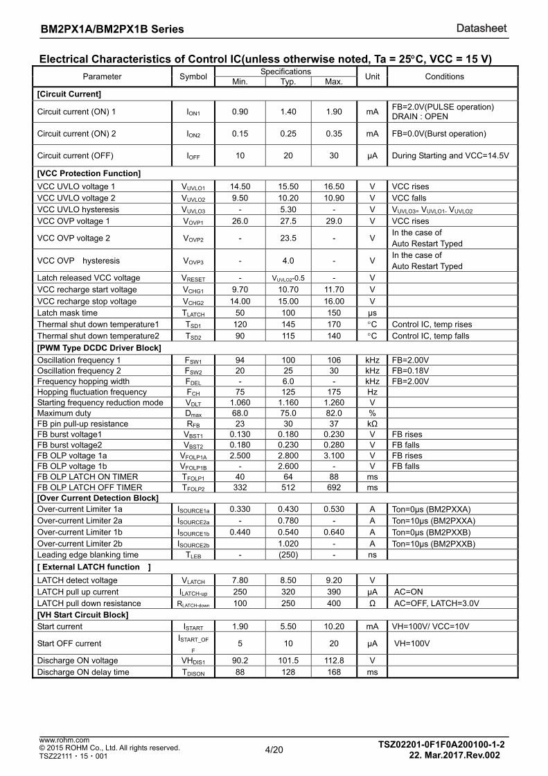
Electrical Characteristics of Control IC(unless otherwise noted, Ta = 25C, VCC = 15 V)
Parameter Symbol Specifications
Unit Conditions Min. Typ. Max.
[Circuit Current]
Circuit current (ON) 1 ION1 0.90 1.40 1.90 mAFB=2.0V(PULSE operation) DRAIN : OPEN
Circuit current (ON) 2 ION2 0.15 0.25 0.35 mA FB=0.0V(Burst operation)
Circuit current (OFF) IOFF 10 20 30 μA During Starting and VCC=14.5V
[VCC Protection Function]
VCC UVLO voltage 1 VUVLO1 14.50 15.50 16.50 V VCC rises VCC UVLO voltage 2 VUVLO2 9.50 10.20 10.90 V VCC falls VCC UVLO hysteresis VUVLO3 - 5.30 - V VUVLO3= VUVLO1- VUVLO2 VCC OVP voltage 1 VOVP1 26.0 27.5 29.0 V VCC rises
VCC OVP voltage 2 VOVP2 - 23.5 - V In the case of Auto Restart Typed
VCC OVP hysteresis VOVP3 - 4.0 - V In the case of Auto Restart Typed
Latch released VCC voltage VRESET - VUVLO2-0.5 - V
VCC recharge start voltage VCHG1 9.70 10.70 11.70 V
VCC recharge stop voltage VCHG2 14.00 15.00 16.00 V Latch mask time TLATCH 50 100 150 μs Thermal shut down temperature1 TSD1 120 145 170 C Control IC, temp rises Thermal shut down temperature2 TSD2 90 115 140 C Control IC, temp falls
[PWM Type DCDC Driver Block]
Oscillation frequency 1 FSW1 94 100 106 kHz FB=2.00V Oscillation frequency 2 FSW2 20 25 30 kHz FB=0.18V Frequency hopping width FDEL - 6.0 - kHz FB=2.00V Hopping fluctuation frequency FCH 75 125 175 Hz Starting frequency reduction mode VDLT 1.060 1.160 1.260 V Maximum duty Dmax 68.0 75.0 82.0 % FB pin pull-up resistance RFB 23 30 37 kΩ FB burst voltage1 VBST1 0.130 0.180 0.230 V FB rises FB burst voltage2 VBST2 0.180 0.230 0.280 V FB falls FB OLP voltage 1a VFOLP1A 2.500 2.800 3.100 V FB rises FB OLP voltage 1b VFOLP1B - 2.600 - V FB falls FB OLP LATCH ON TIMER TFOLP1 40 64 88 ms FB OLP LATCH OFF TIMER TFOLP2 332 512 692 ms [Over Current Detection Block] Over-current Limiter 1a ISOURCE1a 0.330 0.430 0.530 A Ton=0μs (BM2PXXA) Over-current Limiter 2a ISOURCE2a - 0.780 - A Ton=10μs (BM2PXXA) Over-current Limiter 1b ISOURCE1b 0.440 0.540 0.640 A Ton=0μs (BM2PXXB) Over-current Limiter 2b ISOURCE2b 1.020 - A Ton=10μs (BM2PXXB) Leading edge blanking time TLEB - (250) - ns
[ External LATCH function ]
LATCH detect voltage VLATCH 7.80 8.50 9.20 V LATCH pull up current ILATCH-up 250 320 390 μA AC=ON LATCH pull down resistance RLATCH-down 100 250 400 Ω AC=OFF, LATCH=3.0V [VH Start Circuit Block] Start current ISTART 1.90 5.50 10.20 mA VH=100V/ VCC=10V
Start OFF current ISTART_OF
F 5 10 20 μA VH=100V
Discharge ON voltage VHDIS1 90.2 101.5 112.8 V Discharge ON delay time TDISON 88 128 168 ms
5/20
DatasheetDatasheetBM2PX1A/BM2PX1B Series
TSZ02201-0F1F0A200100-1-222. Mar.2017.Rev.002
© 2015 ROHM Co., Ltd. All rights reserved. www.rohm.com
TSZ22111・15・001
Block Description
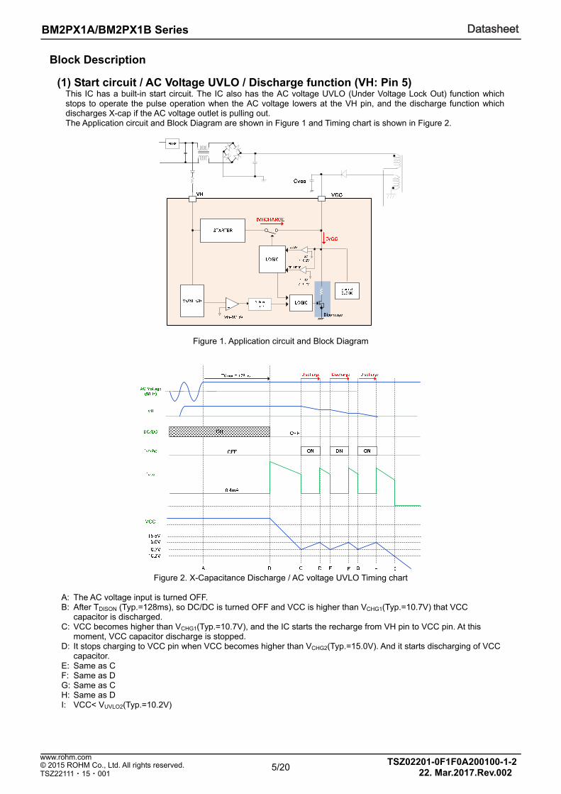
(1) Start circuit / AC Voltage UVLO / Discharge function (VH: Pin 5) This IC has a built-in start circuit. The IC also has the AC voltage UVLO (Under Voltage Lock Out) function which stops to operate the pulse operation when the AC voltage lowers at the VH pin, and the discharge function which discharges X-cap if the AC voltage outlet is pulling out. The Application circuit and Block Diagram are shown in Figure 1 and Timing chart is shown in Figure 2.
Figure 1. Application circuit and Block Diagram
Figure 2. X-Capacitance Discharge / AC voltage UVLO Timing chart
A: The AC voltage input is turned OFF. B: After TDISON (Typ.=128ms), so DC/DC is turned OFF and VCC is higher than VCHG1(Typ.=10.7V) that VCC
capacitor is discharged. C: VCC becomes higher than VCHG1(Typ.=10.7V), and the IC starts the recharge from VH pin to VCC pin. At this
moment, VCC capacitor discharge is stopped. D: It stops charging to VCC pin when VCC becomes higher than VCHG2(Typ.=15.0V). And it starts discharging of VCC
capacitor. E: Same as C F: Same as D G: Same as C H: Same as D I: VCC< VUVLO2(Typ.=10.2V)
6/20
DatasheetDatasheetBM2PX1A/BM2PX1B Series
TSZ02201-0F1F0A200100-1-222. Mar.2017.Rev.002
© 2015 ROHM Co., Ltd. All rights reserved. www.rohm.com
TSZ22111・15・001
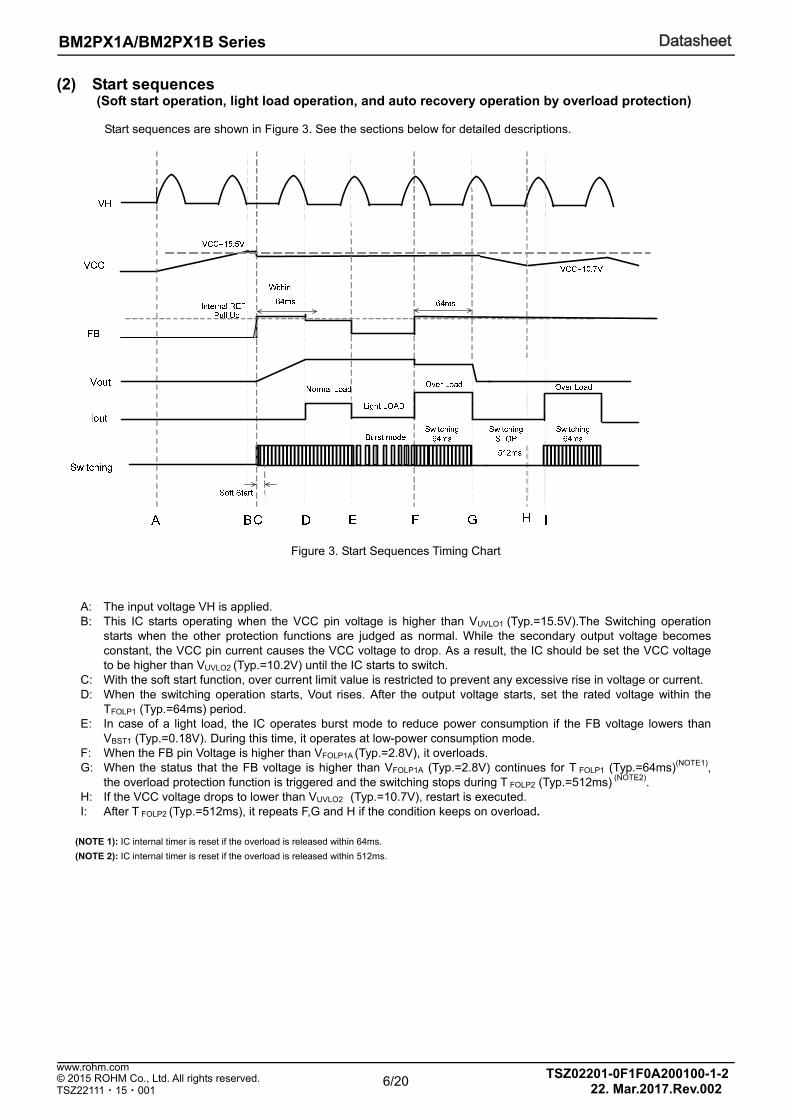
(2) Start sequences (Soft start operation, light load operation, and auto recovery operation by overload protection)
Start sequences are shown in Figure 3. See the sections below for detailed descriptions.
Figure 3. Start Sequences Timing Chart
A: The input voltage VH is applied. B: This IC starts operating when the VCC pin voltage is higher than VUVLO1 (Typ.=15.5V).The Switching operation
starts when the other protection functions are judged as normal. While the secondary output voltage becomes constant, the VCC pin current causes the VCC voltage to drop. As a result, the IC should be set the VCC voltage to be higher than VUVLO2 (Typ.=10.2V) until the IC starts to switch.
C: With the soft start function, over current limit value is restricted to prevent any excessive rise in voltage or current. D: When the switching operation starts, Vout rises. After the output voltage starts, set the rated voltage within the
TFOLP1 (Typ.=64ms) period. E: In case of a light load, the IC operates burst mode to reduce power consumption if the FB voltage lowers than
VBST1 (Typ.=0.18V). During this time, it operates at low-power consumption mode. F: When the FB pin Voltage is higher than VFOLP1A (Typ.=2.8V), it overloads. G: When the status that the FB voltage is higher than VFOLP1A (Typ.=2.8V) continues for T FOLP1 (Typ.=64ms)(NOTE1),
the overload protection function is triggered and the switching stops during T FOLP2 (Typ.=512ms) (NOTE2). H: If the VCC voltage drops to lower than VUVLO2 (Typ.=10.7V), restart is executed. I: After T FOLP2 (Typ.=512ms), it repeats F,G and H if the condition keeps on overload.
(NOTE 1): IC internal timer is reset if the overload is released within 64ms.
(NOTE 2): IC internal timer is reset if the overload is released within 512ms.

7/20
DatasheetDatasheetBM2PX1A/BM2PX1B Series
TSZ02201-0F1F0A200100-1-222. Mar.2017.Rev.002
© 2015 ROHM Co., Ltd. All rights reserved. www.rohm.com
TSZ22111・15・001
(3) VCC pin protection function The IC has a built-in VCC low voltage protection function VCCUVLO (Under Voltage Lock Out), an over voltage protection function VCCOVP (Over Voltage Protection), and a VCC recharge function that operates in case of a drop in VCC voltage. The VCC charge function stabilizes the secondary output voltage charging from high voltage lines by the start circuit when the VCC voltage drops.
VCC UVLO / VCC OVP function VCCUVLO is an auto recovery comparator with a voltage hysteresis. And VCCOVP is a latch Type or auto restart Type comparator. (The type of a latch or auto restart is different by products series.) VCCOVP has a built-in mask time. This detects when the condition that VCC pin voltage is higher than VOVP1 (Typ.=27.5V) continues for TLATCH (Typ.=100us). This function masks such as a surge generated at pin. Figure 4 is showed about the time chart of VCC OVP latch Type
VCC charge function This IC has the recharge function. VCC charge function operates when the VCC voltage drops lower than VCHG1(Typ.=10.7V) after once VCC becomes higher than VUVLO1(Typ.=15.5V) and the IC starts. At that time the VCC pin is charged from the VH pin through the start circuit. Through this operation, BM2PXXA/BM2PXXB prevents failure. When the VCC pin voltage rises higher than VCHG2(Typ.=15.0V) by charging, the IC stops it
Figure 4. VCC UVLO / OVP Timing Chart
A: The VH voltage input, VCC pin voltage starts rising. B: When the VCC voltage is higher than VUVLO1(Typ.=15.5V), VCC UVLO is released and DC/DC operation starts. C: When the VCC voltage is lower than VCHG1 (Typ.=10.7V), VCC charge function operates and the VCC voltage
rises. D: When the VCC voltage is higher than VCHG2 (Typ.=15.0V), VCC charge function stops. E: When the condition that VCC voltage is higher than VOVP1 (Typ.=27.5V), continues for TLATCH (Typ.=100us), the
switching is stopped by the VCCOVP function. F: When the VCC voltage is lower than VOVP2(Typ.=23.5V), DC/DC operation doesn’t restarts because of latch
function. G: The high voltage line VH is drops. H: Same as C I: Same as D J: When the VCC voltage is lower than VUVLO2(Typ.=10.2V), VCC UVLO function operates. K: When the VCC voltage is lower than VRESET(Typ.= VUVLO2-0.5), LATCH function is released.

8/20
DatasheetDatasheetBM2PX1A/BM2PX1B Series
TSZ02201-0F1F0A200100-1-222. Mar.2017.Rev.002
© 2015 ROHM Co., Ltd. All rights reserved. www.rohm.com
TSZ22111・15・001
(4) DCDC driver (PWM comparator, frequency hopping, slope compensation, OSC, burst) This IC has a current mode PWM control. An internal oscillator sets a fixed switching frequency FSW1(Typ.=100kHz) It also has an integrated switching frequency hopping function, which causes the switching frequency to fluctuate. The fluctuation of cycle is FCH (Typ.=125Hz ).
Maximum duty cycle is fixed at Dmax (Typ.=75%). In current mode control, sub-harmonic oscillation may occur when the duty cycle exceeds 50%. As a countermeasure, this IC has built-in slope compensation circuits.
This IC has built-in burst mode and frequency reduction circuits to achieve lower power consumption when the load is light. FB pin is pulled up by RFB (Typ.=30kΩ). FB pin voltage is changed by secondary output voltage (secondary load power). By monitoring the FB pin, burst mode operation and frequency detection start.
Figure 5 shows the FB voltage, and the DC/DC switching frequency operation.
・mode1 : Burst operation ・mode2 : Frequency reduction operation (frequency is reduced) ・mode3 : Fixed frequency operation (operates at max frequency) ・mode4 : Overload operation (stops the pulse operation and starts burst mode)
X
Y
FB [V]
SwitchingFrequency
[ kHz]
0.23V 1.16V
25kHz
100kHz
2.00V
mode 1 mode2 mode 3
2.80V
mode4
Pulse OFF
0.18V
Figure 5. Switching Operation State Changes by FB Pin Voltage

9/20
DatasheetDatasheetBM2PX1A/BM2PX1B Series
TSZ02201-0F1F0A200100-1-222. Mar.2017.Rev.002
© 2015 ROHM Co., Ltd. All rights reserved. www.rohm.com
TSZ22111・15・001
(5) Over Current limiter The IC has a built-in over current limiter per cycle. If the primary coil current exceeds a certain current, switching stops. It also has a built-in AC voltage compensation function. This is the correction function of AC voltage which increases the over current limiter level with time. It is shown in figure 6, 7, and 8.
Figure 6. No AC Voltage Compensation Function Figure 7. Built-in AC Compensation Voltage
Primary peak current is calculated using the formula below. Primary peak current: Ipeak = ISOURCE + Vdc / Lp×Tdelay ISOURCE: Over-current Limiter, Vdc: Input DC voltage, Lp:Primary inductance value, Tdelay: Delay time after detection of over current limiter
Figure 8a. Over Current Limiter (BM2PXXA) Figure 8b. Over Current Limiter (BM2PXXB) (6) Soft start operation
In order to prevent excessive voltage rise and current rise during startup, The IC limits the over current limiter value. The detail is shown in Figure 9. Over current limiter achieves the soft start operation by changing its value with time.
Figure 9a. Soft start (BM2PXXA/Ton=0μs) Figure 9b. Soft start (BM2PXXB/Ton=0μs)

10/20
DatasheetDatasheetBM2PX1A/BM2PX1B Series
TSZ02201-0F1F0A200100-1-222. Mar.2017.Rev.002
© 2015 ROHM Co., Ltd. All rights reserved. www.rohm.com
TSZ22111・15・001
(7) Output over load protection function (FB OLP Comparator) The output overload protection is the function which monitors the secondary output load status by FB pin and stops the switching at over status. In case of overload, current no longer flows to the photo coupler because of the fall of output voltage, so FB voltage rises. If the status that FB voltage is higher than VFOLP1A (Typ.=2.8V) continues for TFOLP1 (Typ.=64ms), IC stops the switching operation judging it is overload. If FB pin drops to lower than VFOLP1B (Typ.=2.6V) from the status that FB pin is higher than VFOLP1A (Typ.=2.8V) within TFOLP1 (Typ.=64ms), the timer of the overload protection is reset. The IC operate switching for TFOLP1 (Typ.=64ms). At starting, FB pin operates from more than VFOLP1A (Typ.=2.8V) because it is pulled up at IC internal voltage. For that, it is necessary for the secondary output voltage to be set the startup time so that FB voltage becomes lower than VFOLP1B (Typ.=2.6V) within TFOLP1 (Typ.=64ms). The returning from once detecting FBOLP is after TFOLP2 (Typ.=512ms).
11/20
DatasheetDatasheetBM2PX1A/BM2PX1B Series
TSZ02201-0F1F0A200100-1-222. Mar.2017.Rev.002
© 2015 ROHM Co., Ltd. All rights reserved. www.rohm.com
TSZ22111・15・001
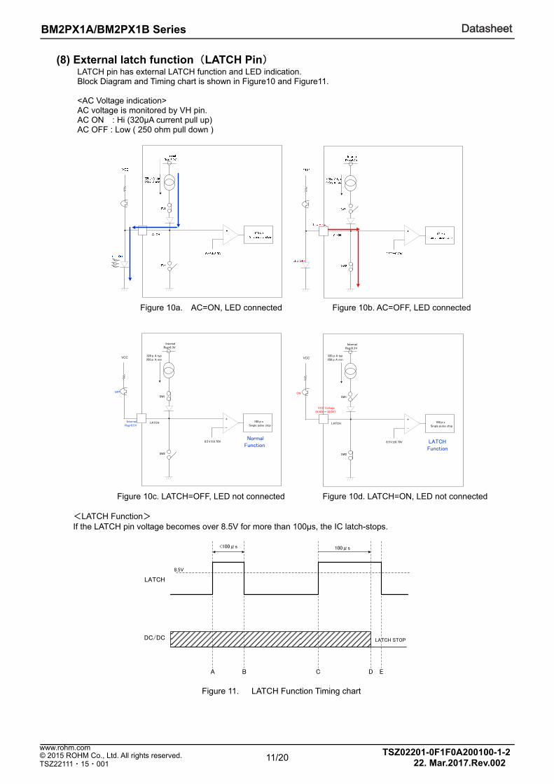
(8) External latch function(LATCH Pin) LATCH pin has external LATCH function and LED indication. Block Diagram and Timing chart is shown in Figure10 and Figure11.
<AC Voltage indication> AC voltage is monitored by VH pin. AC ON : Hi (320μA current pull up) AC OFF : Low ( 250 ohm pull down )
Figure 10a. AC=ON, LED connected Figure 10b. AC=OFF, LED connected
Internal Reg=6.3V
SW1
SW2
+
-
100μsSingle pulse stop
LATCH
8.5V±0.70V
VCC
Internal Reg=6.3V
SW1
SW2
+
-
100μsSingle pulse stop
LATCH
8.5V±0.70V
VCC
OFF
Normal Function
ON
VCC Voltage(9.50V~32.0V)
Internal Reg=6.5V
LATCHFunction
320μA typ250μA min
320μA typ250μ A min
Figure 10c. LATCH=OFF, LED not connected Figure 10d. LATCH=ON, LED not connected
<LATCH Function> If the LATCH pin voltage becomes over 8.5V for more than 100μs, the IC latch-stops.
LATCH
<100μs
8.5V
DC/DC
A B C D E
LATCH STOP
100μs
Figure 11. LATCH Function Timing chart

12/20
DatasheetDatasheetBM2PX1A/BM2PX1B Series
TSZ02201-0F1F0A200100-1-222. Mar.2017.Rev.002
© 2015 ROHM Co., Ltd. All rights reserved. www.rohm.com
TSZ22111・15・001
Operation mode of protection circuit Operation mode of protection functions are shown in Table 1.
Table 1. Operation Mode of Protection Circuit
Function Operation mode
VCC Under Voltage Locked Out Auto recovery
VCC Over Voltage Protection Auto recovery/Latch(with 100μs timer)
Thermal Shut Down Auto recovery(with 100μs timer)
FB Over Limited Protection Auto recovery/Latch(with 64ms timer)

13/20
DatasheetDatasheetBM2PX1A/BM2PX1B Series
TSZ02201-0F1F0A200100-1-222. Mar.2017.Rev.002
© 2015 ROHM Co., Ltd. All rights reserved. www.rohm.com
TSZ22111・15・001
Thermal loss The thermal design should set the operation for the following conditions. (Since the temperature shown below is the guaranteed temperature, be sure to take into account a sufficient margin.)
1. The ambient temperature Ta must be 105 or less. 2. The IC’s loss must be within the allowable dissipation Pd.
The thermal dissipation characteristics are as follows. (PCB: 114.5 mm × 101.5mm × 1.6 mm, mounted on glass epoxy single-layer substrate)
Figure 12. Thermal Dissipation Characteristics
0.0
0.2
0.4
0.6
0.8
1.0
1.2
1.4
1.6
0 25 50 75 100 125 150
Pd[
W]
Ta[]

14/20
DatasheetDatasheetBM2PX1A/BM2PX1B Series
TSZ02201-0F1F0A200100-1-222. Mar.2017.Rev.002
© 2015 ROHM Co., Ltd. All rights reserved. www.rohm.com
TSZ22111・15・001
I/O Equivalent Circuit Diagram
8
GND VCC
7 DRAIN
1 FB2
DRAIN
VCC
3 LATCH
5 VH
4
DRAIN
GND
Internal MOSFET
FB
InternalCircuit
VCC
6 DRAIN
DRAIN
GND
Internal MOSFET
DRAIN
GND
Internal MOSFET
VH
LATCH
GND
GNDGND
VCC
VCC
GND GND
VCC
GND
VCC
GND
15/20
DatasheetDatasheetBM2PX1A/BM2PX1B Series
TSZ02201-0F1F0A200100-1-222. Mar.2017.Rev.002
© 2015 ROHM Co., Ltd. All rights reserved. www.rohm.com
TSZ22111・15・001
0.15
0.17
0.19
0.21
0.23
0.25
0.27
0.29
0.31
-40 -20 0 20 40 60 80 100 120
Cir
cu
it C
urr
en
t(O
N2
) [
mA
]
Tempature []
949596979899
100101102103104105106
-40 -20 0 20 40 60 80 100 120
Osc
illa
tio
n f
req
ue
nc
y 1
[kH
z]
Tempature []
20
22
24
26
28
30
-40 -20 0 20 40 60 80 100 120
Os
cill
atio
n f
req
uen
cy
2 [k
Hz]
Tempature []
9.5
9.6
9.7
9.8
9.9
10.0
10.1
10.2
10.3
10.4
10.5
-40 -20 0 20 40 60 80 100 120
VC
C U
VL
O v
olt
ag
e 2
[V
]
Tempature []
50
60
70
80
90
100
110
120
130
140
150
-40 -20 0 20 40 60 80 100 120
La
tch
mas
k ti
me
[μs
]
Tempature []
10.0
12.5
15.0
17.5
20.0
22.5
25.0
27.5
30.0
-40 -20 0 20 40 60 80 100 120
Cir
cu
it C
urr
en
t (O
FF
)[μ
A]
Tempature []
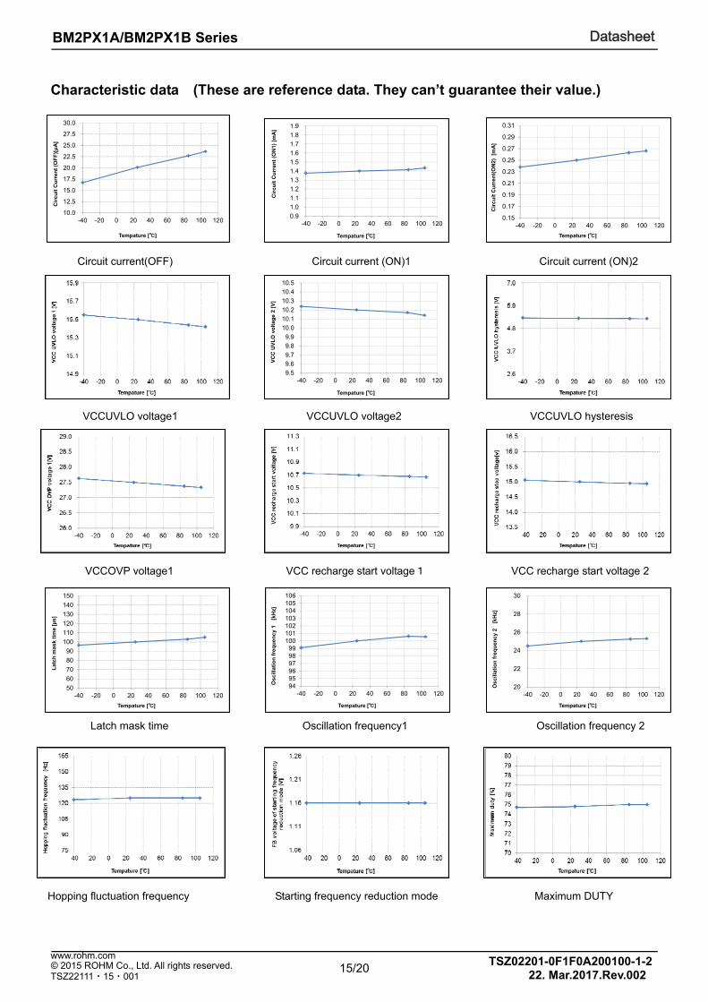
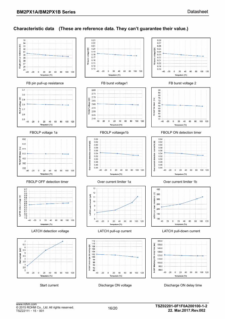
Characteristic data (These are reference data. They can’t guarantee their value.)
Circuit current(OFF) Circuit current (ON)1 Circuit current (ON)2
VCCUVLO voltage1 VCCUVLO voltage2 VCCUVLO hysteresis
VCCOVP voltage1 VCC recharge start voltage1 VCC recharge start voltage 2
Latch mask time Oscillation frequency1 Oscillation frequency 2
Hopping fluctuation frequency Starting frequency reduction mode Maximum DUTY
0.9
1.0
1.1
1.2
1.3
1.4
1.5
1.6
1.7
1.8
1.9
-40 -20 0 20 40 60 80 100 120
Cir
cuit
Cu
rren
t (O
N1)
[m
A]
Tempature []
16/20
DatasheetDatasheetBM2PX1A/BM2PX1B Series
TSZ02201-0F1F0A200100-1-222. Mar.2017.Rev.002
© 2015 ROHM Co., Ltd. All rights reserved. www.rohm.com
TSZ22111・15・001
0.44
0.46
0.48
0.50
0.52
0.54
0.56
0.58
0.60
0.62
0.64
-40 -20 0 20 40 60 80 100 120Ove
r-cu
rren
t d
ete
cti
on
cu
rre
nt1
a[A
]
Tempature []
0.44
0.46
0.48
0.50
0.52
0.54
0.56
0.58
0.60
0.62
0.64
-40 -20 0 20 40 60 80 100 120Ove
r-cu
rren
t d
ete
ctio
n c
urr
ne
t1b
[A
]
Tempature []
Characteristic data (These are reference data. They can’t guarantee their value.)
FB pin pull-up resistance FB burst voltage1 FB burst voltage 2
FBOLP voltage 1a FBOLP voltaege1b FBOLP ON detection timer
FBOLP OFF detection timer Over current limiter 1a Over current limiter 1b
LATCH detection voltage LATCH pull-up current LATCH pull-down current
Start current Discharge ON voltage Discharge ON delay time
6
7
8
9
10
11
12
13
-40 -20 0 20 40 60 80 100 120
LA
TC
H L
eak
Cu
rren
t [μ
A]
Tempature []
17/20
DatasheetDatasheetBM2PX1A/BM2PX1B Series
TSZ02201-0F1F0A200100-1-222. Mar.2017.Rev.002
© 2015 ROHM Co., Ltd. All rights reserved. www.rohm.com
TSZ22111・15・001
Operational Notes
1. Reverse Connection of Power Supply Connecting the power supply in reverse polarity can damage the IC. Take precautions against reverse polarity when connecting the power supply, such as mounting an external diode between the power supply and the IC’s power supply terminals.
2. Power Supply Lines
Design the PCB layout pattern to provide low impedance supply lines. Separate the GND and supply lines of the digital and analog blocks to prevent noise in the GND and supply lines of the digital block from affecting the analog block. Furthermore, connect a capacitor to GND at all power supply pins. Consider the effect of temperature and aging on the capacitance value when using electrolytic capacitors.
3. GND Voltage Ensure that no pins are at a voltage below that of the GND pin at any time, even during transient condition.
4. GND Wiring Pattern When using both small-signal and large-current GND traces, the two GND traces should be routed separately but connected to a single GND at the reference point of the application board to avoid fluctuations in the small-signal GND caused by large currents. Also ensure that the GND traces of external components do not cause variations on the GND voltage. The GND lines must be as short and thick as possible to reduce line impedance.
5. Thermal Consideration Should by any chance the power dissipation rating be exceeded, the rise in temperature of the chip may result in deterioration of the properties of the chip. The absolute maximum rating of the Pd stated in this specification is when the IC is mounted on a 70mm x 70mm x 1.6mm glass epoxy board. In case of exceeding this absolute maximum rating, increase the board size and copper area to prevent exceeding the Pd rating.
6. Recommended Operating Conditions These conditions represent a range within which the expected characteristics of the IC can be approximately obtained. The electrical characteristics are guaranteed under the conditions of each parameter.
7. Inrush Current When power is first supplied to the IC, it is possible that the internal logic may be unstable and inrush current may flow instantaneously due to the internal powering sequence and delays, especially if the IC has more than one power supply. Therefore, give special consideration to power coupling capacitance, power wiring, width of GND wiring, and routing of connections.
8. Operation Under Strong Electromagnetic Field
Operating the IC in the presence of a strong electromagnetic field may cause the IC to malfunction.
9. Testing on Application Boards When testing the IC on an application board, connecting a capacitor directly to a low-impedance output pin may subject the IC to stress. Always discharge capacitors completely after each process or step. The IC’s power supply should always be turned OFF completely before connecting or removing it from the test setup during the inspection process. To prevent damage from static discharge, GND the IC during assembly and use similar precautions during transport and storage.
10. Inter-pin Short and Mounting Errors Ensure that the direction and position are correct when mounting the IC on the PCB. Incorrect mounting may result in damaging the IC. Avoid nearby pins being shorted to each other especially to GND, power supply and output pin. Inter-pin shorts could be due to many reasons such as metal particles, water droplets (in very humid environment) and unintentional solder bridge deposited in between pins during assembly to name a few.
11. Unused Input Terminals
Input terminals of an IC are often connected to the gate of a MOS transistor. The gate has extremely high impedance and extremely low capacitance. If left unconnected, the electric field from the outside can easily charge it. The small charge acquired in this way is enough to produce a significant effect on the conduction through the transistor and cause unexpected operation of the IC. So unless otherwise specified, unused input terminals should be connected to the power supply or GND line.
18/20
DatasheetDatasheetBM2PX1A/BM2PX1B Series
TSZ02201-0F1F0A200100-1-222. Mar.2017.Rev.002
© 2015 ROHM Co., Ltd. All rights reserved. www.rohm.com
TSZ22111・15・001
Operational Notes – continued
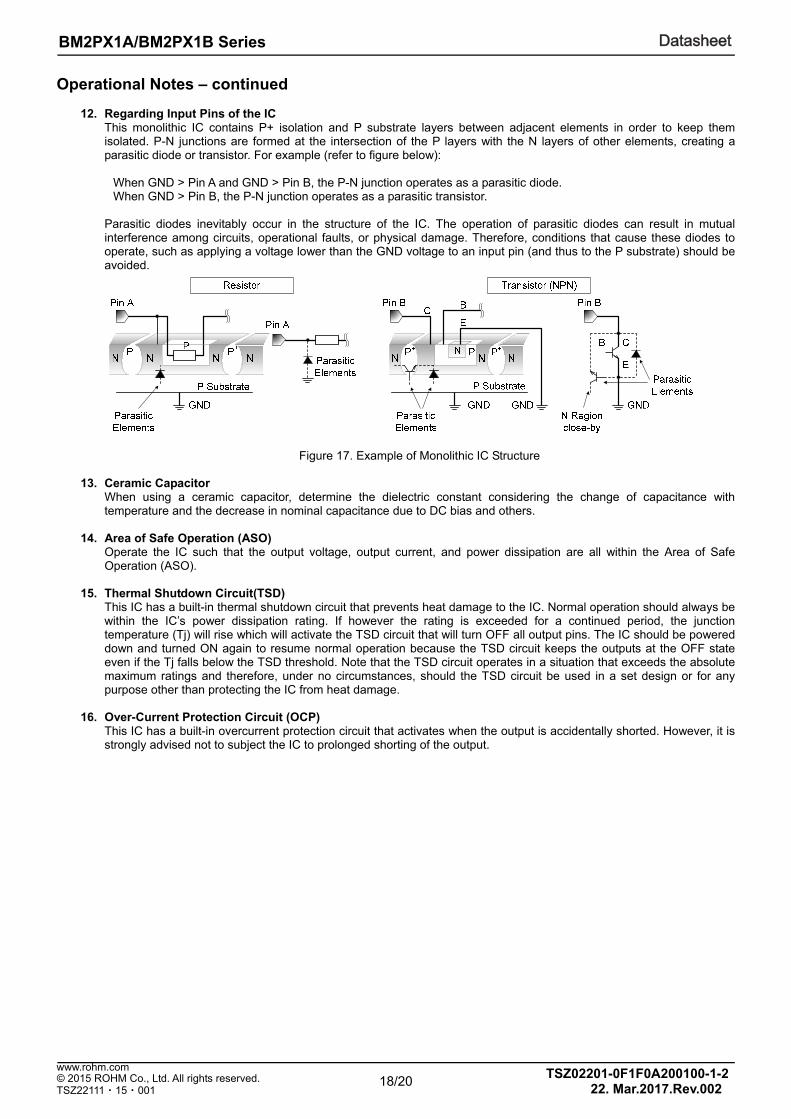
12. Regarding Input Pins of the IC This monolithic IC contains P+ isolation and P substrate layers between adjacent elements in order to keep them isolated. P-N junctions are formed at the intersection of the P layers with the N layers of other elements, creating a parasitic diode or transistor. For example (refer to figure below):
When GND > Pin A and GND > Pin B, the P-N junction operates as a parasitic diode. When GND > Pin B, the P-N junction operates as a parasitic transistor.
Parasitic diodes inevitably occur in the structure of the IC. The operation of parasitic diodes can result in mutual interference among circuits, operational faults, or physical damage. Therefore, conditions that cause these diodes to operate, such as applying a voltage lower than the GND voltage to an input pin (and thus to the P substrate) should be avoided.
Figure 17. Example of Monolithic IC Structure
13. Ceramic Capacitor
When using a ceramic capacitor, determine the dielectric constant considering the change of capacitance with temperature and the decrease in nominal capacitance due to DC bias and others.
14. Area of Safe Operation (ASO) Operate the IC such that the output voltage, output current, and power dissipation are all within the Area of Safe Operation (ASO).
15. Thermal Shutdown Circuit(TSD) This IC has a built-in thermal shutdown circuit that prevents heat damage to the IC. Normal operation should always be within the IC’s power dissipation rating. If however the rating is exceeded for a continued period, the junction temperature (Tj) will rise which will activate the TSD circuit that will turn OFF all output pins. The IC should be powered down and turned ON again to resume normal operation because the TSD circuit keeps the outputs at the OFF state even if the Tj falls below the TSD threshold. Note that the TSD circuit operates in a situation that exceeds the absolute maximum ratings and therefore, under no circumstances, should the TSD circuit be used in a set design or for any purpose other than protecting the IC from heat damage.
16. Over-Current Protection Circuit (OCP)
This IC has a built-in overcurrent protection circuit that activates when the output is accidentally shorted. However, it is strongly advised not to subject the IC to prolonged shorting of the output.
19/20
DatasheetDatasheetBM2PX1A/BM2PX1B Series
TSZ02201-0F1F0A200100-1-222. Mar.2017.Rev.002
© 2015 ROHM Co., Ltd. All rights reserved. www.rohm.com
TSZ22111・15・001
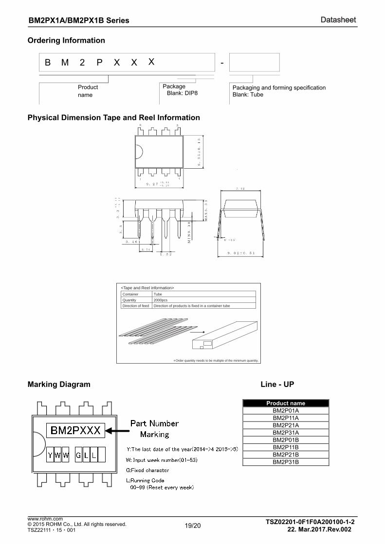
Ordering Information
B M 2 P X X X -
Product name
Package Blank: DIP8
Packaging and forming specification Blank: Tube
Physical Dimension Tape and Reel Information
Marking Diagram Line - UP
Product name BM2P01A BM2P11A BM2P21A BM2P31A BM2P01B BM2P11B BM2P21B BM2P31B
∗ Order quantity needs to be multiple of the minimum quantity.
<Tape and Reel information>
TubeContainer
Quantity
Direction of feed
2000pcs
Direction of products is fixed in a container tube

20/20
DatasheetDatasheetBM2PX1A/BM2PX1B Series
TSZ02201-0F1F0A200100-1-222. Mar.2017.Rev.002
© 2015 ROHM Co., Ltd. All rights reserved. www.rohm.com
TSZ22111・15・001
Revision History
Date Revision Changes
16.Nov.2015 001 New Release
22.Mar.2017 002
P1 a value of basic specifications P3 a value of operating conditions P8 a value of Figure5 P11 a value of external latch function
Notice-PGA-E Rev.003
© 2015 ROHM Co., Ltd. All rights reserved.
Notice
Precaution on using ROHM Products 1. Our Products are designed and manufactured for application in ordinary electronic equipments (such as AV equipment,
OA equipment, telecommunication equipment, home electronic appliances, amusement equipment, etc.). If you intend to use our Products in devices requiring extremely high reliability (such as medical equipment
(Note 1), transport
equipment, traffic equipment, aircraft/spacecraft, nuclear power controllers, fuel controllers, car equipment including car accessories, safety devices, etc.) and whose malfunction or failure may cause loss of human life, bodily injury or serious damage to property (“Specific Applications”), please consult with the ROHM sales representative in advance. Unless otherwise agreed in writing by ROHM in advance, ROHM shall not be in any way responsible or liable for any damages, expenses or losses incurred by you or third parties arising from the use of any ROHM’s Products for Specific Applications.
(Note1) Medical Equipment Classification of the Specific Applications
JAPAN USA EU CHINA
CLASSⅢ CLASSⅢ
CLASSⅡb CLASSⅢ
CLASSⅣ CLASSⅢ
2. ROHM designs and manufactures its Products subject to strict quality control system. However, semiconductor
products can fail or malfunction at a certain rate. Please be sure to implement, at your own responsibilities, adequate safety measures including but not limited to fail-safe design against the physical injury, damage to any property, which a failure or malfunction of our Products may cause. The following are examples of safety measures:
[a] Installation of protection circuits or other protective devices to improve system safety [b] Installation of redundant circuits to reduce the impact of single or multiple circuit failure
3. Our Products are designed and manufactured for use under standard conditions and not under any special or extraordinary environments or conditions, as exemplified below. Accordingly, ROHM shall not be in any way responsible or liable for any damages, expenses or losses arising from the use of any ROHM’s Products under any special or extraordinary environments or conditions. If you intend to use our Products under any special or extraordinary environments or conditions (as exemplified below), your independent verification and confirmation of product performance, reliability, etc, prior to use, must be necessary:
[a] Use of our Products in any types of liquid, including water, oils, chemicals, and organic solvents [b] Use of our Products outdoors or in places where the Products are exposed to direct sunlight or dust [c] Use of our Products in places where the Products are exposed to sea wind or corrosive gases, including Cl2,
H2S, NH3, SO2, and NO2
[d] Use of our Products in places where the Products are exposed to static electricity or electromagnetic waves [e] Use of our Products in proximity to heat-producing components, plastic cords, or other flammable items [f] Sealing or coating our Products with resin or other coating materials [g] Use of our Products without cleaning residue of flux (even if you use no-clean type fluxes, cleaning residue of
flux is recommended); or Washing our Products by using water or water-soluble cleaning agents for cleaning residue after soldering
[h] Use of the Products in places subject to dew condensation
4. The Products are not subject to radiation-proof design. 5. Please verify and confirm characteristics of the final or mounted products in using the Products. 6. In particular, if a transient load (a large amount of load applied in a short period of time, such as pulse. is applied,
confirmation of performance characteristics after on-board mounting is strongly recommended. Avoid applying power exceeding normal rated power; exceeding the power rating under steady-state loading condition may negatively affect product performance and reliability.
7. De-rate Power Dissipation depending on ambient temperature. When used in sealed area, confirm that it is the use in
the range that does not exceed the maximum junction temperature. 8. Confirm that operation temperature is within the specified range described in the product specification. 9. ROHM shall not be in any way responsible or liable for failure induced under deviant condition from what is defined in
this document.
Precaution for Mounting / Circuit board design 1. When a highly active halogenous (chlorine, bromine, etc.) flux is used, the residue of flux may negatively affect product
performance and reliability.
2. In principle, the reflow soldering method must be used on a surface-mount products, the flow soldering method must be used on a through hole mount products. If the flow soldering method is preferred on a surface-mount products, please consult with the ROHM representative in advance.
For details, please refer to ROHM Mounting specification

Notice-PGA-E Rev.003
© 2015 ROHM Co., Ltd. All rights reserved.
Precautions Regarding Application Examples and External Circuits 1. If change is made to the constant of an external circuit, please allow a sufficient margin considering variations of the
characteristics of the Products and external components, including transient characteristics, as well as static characteristics.
2. You agree that application notes, reference designs, and associated data and information contained in this document
are presented only as guidance for Products use. Therefore, in case you use such information, you are solely responsible for it and you must exercise your own independent verification and judgment in the use of such information contained in this document. ROHM shall not be in any way responsible or liable for any damages, expenses or losses incurred by you or third parties arising from the use of such information.
Precaution for Electrostatic This Product is electrostatic sensitive product, which may be damaged due to electrostatic discharge. Please take proper caution in your manufacturing process and storage so that voltage exceeding the Products maximum rating will not be applied to Products. Please take special care under dry condition (e.g. Grounding of human body / equipment / solder iron, isolation from charged objects, setting of Ionizer, friction prevention and temperature / humidity control).
Precaution for Storage / Transportation 1. Product performance and soldered connections may deteriorate if the Products are stored in the places where:
[a] the Products are exposed to sea winds or corrosive gases, including Cl2, H2S, NH3, SO2, and NO2 [b] the temperature or humidity exceeds those recommended by ROHM [c] the Products are exposed to direct sunshine or condensation [d] the Products are exposed to high Electrostatic
2. Even under ROHM recommended storage condition, solderability of products out of recommended storage time period may be degraded. It is strongly recommended to confirm solderability before using Products of which storage time is exceeding the recommended storage time period.
3. Store / transport cartons in the correct direction, which is indicated on a carton with a symbol. Otherwise bent leads
may occur due to excessive stress applied when dropping of a carton. 4. Use Products within the specified time after opening a humidity barrier bag. Baking is required before using Products of
which storage time is exceeding the recommended storage time period.
Precaution for Product Label A two-dimensional barcode printed on ROHM Products label is for ROHM’s internal use only.
Precaution for Disposition When disposing Products please dispose them properly using an authorized industry waste company.
Precaution for Foreign Exchange and Foreign Trade act Since concerned goods might be fallen under listed items of export control prescribed by Foreign exchange and Foreign trade act, please consult with ROHM in case of export.
Precaution Regarding Intellectual Property Rights 1. All information and data including but not limited to application example contained in this document is for reference
only. ROHM does not warrant that foregoing information or data will not infringe any intellectual property rights or any other rights of any third party regarding such information or data.
2. ROHM shall not have any obligations where the claims, actions or demands arising from the combination of the Products with other articles such as components, circuits, systems or external equipment (including software).
3. No license, expressly or implied, is granted hereby under any intellectual property rights or other rights of ROHM or any third parties with respect to the Products or the information contained in this document. Provided, however, that ROHM will not assert its intellectual property rights or other rights against you or your customers to the extent necessary to manufacture or sell products containing the Products, subject to the terms and conditions herein.
Other Precaution 1. This document may not be reprinted or reproduced, in whole or in part, without prior written consent of ROHM.
2. The Products may not be disassembled, converted, modified, reproduced or otherwise changed without prior written consent of ROHM.
3. In no event shall you use in any way whatsoever the Products and the related technical information contained in the Products or this document for any military purposes, including but not limited to, the development of mass-destruction weapons.
4. The proper names of companies or products described in this document are trademarks or registered trademarks of ROHM, its affiliated companies or third parties.

DatasheetDatasheet
Notice – WE Rev.001© 2015 ROHM Co., Ltd. All rights reserved.
General Precaution 1. Before you use our Pro ducts, you are requested to care fully read this document and fully understand its contents.
ROHM shall n ot be in an y way responsible or liabl e for fa ilure, malfunction or acci dent arising from the use of a ny ROHM’s Products against warning, caution or note contained in this document.
2. All information contained in this docume nt is current as of the issuing date and subj ect to change without any prior
notice. Before purchasing or using ROHM’s Products, please confirm the la test information with a ROHM sale s representative.
3. The information contained in this doc ument is provi ded on an “as is” basis and ROHM does not warrant that all
information contained in this document is accurate an d/or error-free. ROHM shall not be in an y way responsible or liable for any damages, expenses or losses incurred by you or third parties resulting from inaccuracy or errors of or concerning such information.