
Accurate Shielded Interconnect Delay Estimation by ...
10
IEEE TRANSACTIONS ON CIRCUITS AND SYSTEMS–I: REGULAR PAPERS, VOL. 65, NO. 10, OCTOBER 2018 3435 Accurate Shielded Interconnect Delay Estimation by Reconfigurable Ring Oscillator Eyal Sarfati, Binyamin Frankel, Yitzhak Birk, Senior Member, IEEE, and Shmuel Wimer , Member, IEEE Abstract—Shielding, which is used in VLSI designs to prevent noise interference from the cross-coupling capacitance between adjacent signals can also be used to tune the propagation delay of the clock signals in designs operating at low GHz frequencies. This paper presents a detailed design for a 16-nm ring oscillator with built-in reconfigurable shielding, and a delay estimation methodology. Together these provide a post-silicon measurement methodology that can derive accurate shielding delays without any direct delay measurements. The shielded ring oscillator and the testing methodology are designed to minimize the effects of on-die variations on estimation accuracy. Comparisons of the estimated delays with SPICE simulations show very good fit across process technology corners. The circuit was fabricated in 16-nm technology. The accuracy and robustness of the estimation methodology were verified by cross-validation, obtained from both pre and post-silicon measurements. Index Terms— Integrated circuit interconnections, parameter estimation, ring oscillator, wire shielding. I. I NTRODUCTION I NTERCONNECT shielding is used in Very Large Scale Integration (VLSI) designs to prevent noise interference between signals. The clock signals spread over the entire silicon die to synchronize the operation of the underlying circuits in digital systems are the noisiest, and hence are shielded. They are a source of signal integrity problems, which can be avoided by extensive usage of shielding [1]. Clock signals connected to each sequential element (e.g., latch, flip- flop) are sometimes delayed with respect to each other. This is done by inserting delay buffers into the clock distribution network [2]–[5], among others. Often, intentional delay buffers are also inserted into logic signal paths to solve min-delay (hold) problems [6]. The internal delay of the buffers is subject to wide, unpredictable changes due to process variation, and this has been aggravated by recent progress in reducing VLSI technologies to the nanometer scale [7], [8]. Manuscript received February 27, 2018; revised April 8, 2018; accepted April 9, 2018. Date of publication April 26, 2018; date of current version August 30, 2018. This work was supported in part by the Israel Chief Scientist under the HiPer Consortium of the MAGNET Program and in part by the Marvell Corporate. This paper was recommended by Associate Editor E. Blokhina. (Corresponding author: Shmuel Wimer.) E. Sarfati and Y. Birk are with the Electrical Engineering Depart- ment, Technion, Haifa 32000, Israel (e-mail: [email protected]; [email protected]). B. Frankel and S. Wimer are with the Engineering Faculty, Bar-Ilan University, Ramat-Gan 52900, Israel (e-mail: [email protected]; [email protected]). Color versions of one or more of the figures in this paper are available online at http://ieeexplore.ieee.org. Digital Object Identifier 10.1109/TCSI.2018.2825999 Using shields as delay elements requires knowledge of their behavior in real silicon, which may be quite different from the delays obtained in RC layout extraction and SPICE simulations. Due to the lack of observability of internal nodes, direct delay measurements in silicon are very expensive, and in many cases impossible. Hence, there is a real need for indirect measurement of shielding delay effects. To the best of our knowledge, a post-silicon measurement and a methodology that can provide an accurate estimate of the in-circuit shielding impact on delays has not yet been proposed. An early study on ways to lessen the cross-coupling delay burden incurred by shielding by allowing variable spacing was presented in [9] and [10]. In a recent work, Frankel and Wimer [11] proposed tapering the space of the clock shielding wires to solve the clock tuning problem by useful skew as an alternative to the insertion of expensive delay buffers. It was shown that the optimal space tapering yielding the desired propagation delay with minimum area consumption was proportional to the square root of the distance from the driver to the receiver. A later work [12] turned shield insertion into a practical clock tuning design flow as a part of the backend clock tree synthesis (CTS). The authors showed that for a memory controller and an ARM ® -based processor, about 90% of the useful skew insertion prerequisites could be solved by appropriate shielding implementation. This work examined the impact of process variations on intentional required skew propagation delays [13]. It was shown in [12] that delays obtained by shields were 50% less sensitive to variations than those obtained by delay buffers. The other advantages of using shields rather than delay buffers such as the ease of late design changes (ECOs) were also discussed. The main contributions of this paper are the following: • a special reconfigurable ring oscillator accompanied by a testing circuit to measure the delay effect of shielding on silicon, • a verified methodology that enables an accurate post- silicon estimation of the shielding impact on delays, • a demonstration that delay tuning by shielding is possible over a wide range, and • post-silicon measurements on 16nm test-chip, which con- firmed the validity of the above. The remainder of this paper is organized as follows. Section II discusses delay tuning by shielding. Section III proposes a special ring oscillator and a test circuit to indirectly measure shield delays on silicon. Section IV presents an 1549-8328 © 2018 IEEE. Personal use is permitted, but republication/redistribution requires IEEE permission. See http://www.ieee.org/publications_standards/publications/rights/index.html for more information.
Transcript of Accurate Shielded Interconnect Delay Estimation by ...

IEEE TRANSACTIONS ON CIRCUITS AND SYSTEMS–I: REGULAR PAPERS, VOL. 65, NO. 10, OCTOBER 2018 3435
Accurate Shielded Interconnect Delay Estimationby Reconfigurable Ring Oscillator
Eyal Sarfati, Binyamin Frankel, Yitzhak Birk, Senior Member, IEEE, and Shmuel Wimer , Member, IEEE
Abstract— Shielding, which is used in VLSI designs to preventnoise interference from the cross-coupling capacitance betweenadjacent signals can also be used to tune the propagationdelay of the clock signals in designs operating at low GHzfrequencies. This paper presents a detailed design for a 16-nmring oscillator with built-in reconfigurable shielding, and a delayestimation methodology. Together these provide a post-siliconmeasurement methodology that can derive accurate shieldingdelays without any direct delay measurements. The shieldedring oscillator and the testing methodology are designed tominimize the effects of on-die variations on estimation accuracy.Comparisons of the estimated delays with SPICE simulationsshow very good fit across process technology corners. The circuitwas fabricated in 16-nm technology. The accuracy and robustnessof the estimation methodology were verified by cross-validation,obtained from both pre and post-silicon measurements.
Index Terms— Integrated circuit interconnections, parameterestimation, ring oscillator, wire shielding.
I. INTRODUCTION
INTERCONNECT shielding is used in Very Large ScaleIntegration (VLSI) designs to prevent noise interference
between signals. The clock signals spread over the entiresilicon die to synchronize the operation of the underlyingcircuits in digital systems are the noisiest, and hence areshielded. They are a source of signal integrity problems, whichcan be avoided by extensive usage of shielding [1]. Clocksignals connected to each sequential element (e.g., latch, flip-flop) are sometimes delayed with respect to each other. Thisis done by inserting delay buffers into the clock distributionnetwork [2]–[5], among others. Often, intentional delay buffersare also inserted into logic signal paths to solve min-delay(hold) problems [6]. The internal delay of the buffers is subjectto wide, unpredictable changes due to process variation, andthis has been aggravated by recent progress in reducing VLSItechnologies to the nanometer scale [7], [8].
Manuscript received February 27, 2018; revised April 8, 2018; acceptedApril 9, 2018. Date of publication April 26, 2018; date of current versionAugust 30, 2018. This work was supported in part by the Israel ChiefScientist under the HiPer Consortium of the MAGNET Program and in partby the Marvell Corporate. This paper was recommended by Associate EditorE. Blokhina. (Corresponding author: Shmuel Wimer.)
E. Sarfati and Y. Birk are with the Electrical Engineering Depart-ment, Technion, Haifa 32000, Israel (e-mail: [email protected];[email protected]).
B. Frankel and S. Wimer are with the Engineering Faculty, Bar-IlanUniversity, Ramat-Gan 52900, Israel (e-mail: [email protected];[email protected]).
Color versions of one or more of the figures in this paper are availableonline at http://ieeexplore.ieee.org.
Digital Object Identifier 10.1109/TCSI.2018.2825999
Using shields as delay elements requires knowledge oftheir behavior in real silicon, which may be quite differentfrom the delays obtained in RC layout extraction and SPICEsimulations. Due to the lack of observability of internal nodes,direct delay measurements in silicon are very expensive, and inmany cases impossible. Hence, there is a real need for indirectmeasurement of shielding delay effects. To the best of ourknowledge, a post-silicon measurement and a methodologythat can provide an accurate estimate of the in-circuit shieldingimpact on delays has not yet been proposed.
An early study on ways to lessen the cross-couplingdelay burden incurred by shielding by allowing variablespacing was presented in [9] and [10]. In a recent work,Frankel and Wimer [11] proposed tapering the space of theclock shielding wires to solve the clock tuning problem byuseful skew as an alternative to the insertion of expensive delaybuffers. It was shown that the optimal space tapering yieldingthe desired propagation delay with minimum area consumptionwas proportional to the square root of the distance from thedriver to the receiver.
A later work [12] turned shield insertion into a practicalclock tuning design flow as a part of the backend clocktree synthesis (CTS). The authors showed that for a memorycontroller and an ARM®-based processor, about 90% ofthe useful skew insertion prerequisites could be solved byappropriate shielding implementation. This work examinedthe impact of process variations on intentional required skewpropagation delays [13]. It was shown in [12] that delaysobtained by shields were 50% less sensitive to variations thanthose obtained by delay buffers. The other advantages of usingshields rather than delay buffers such as the ease of late designchanges (ECOs) were also discussed.
The main contributions of this paper are the following:• a special reconfigurable ring oscillator accompanied by a
testing circuit to measure the delay effect of shielding onsilicon,
• a verified methodology that enables an accurate post-silicon estimation of the shielding impact on delays,
• a demonstration that delay tuning by shielding is possibleover a wide range, and
• post-silicon measurements on 16nm test-chip, which con-firmed the validity of the above.
The remainder of this paper is organized as follows.Section II discusses delay tuning by shielding. Section IIIproposes a special ring oscillator and a test circuit to indirectlymeasure shield delays on silicon. Section IV presents an
1549-8328 © 2018 IEEE. Personal use is permitted, but republication/redistribution requires IEEE permission.See http://www.ieee.org/publications_standards/publications/rights/index.html for more information.

3436 IEEE TRANSACTIONS ON CIRCUITS AND SYSTEMS–I: REGULAR PAPERS, VOL. 65, NO. 10, OCTOBER 2018
Fig. 1. Driver-to-receiver interconnect (a) and its RC-ladder modeling (b).
Fig. 2. Shielded interconnect modeling.
estimation methodology to obtain the delays of various shieldsin the internal, unobservable segments of the ring oscillator.Section V compares the estimated delays to simulated delays,and also demonstrates the robustness and validity of the entireestimation methodology. Section VI presents the post-siliconmeasurement results and Section VII draws conclusions.
II. DELAY TUNING BY TAPERING OF
INTERCONNECTION SHIELDING
The Elmore delay model [14] has been widely used inVLSI design since its early days to calculate the interconnectdelay [15]. Consider Fig. 1(a), where a driver connected on thenear end sends a signal along a wire to a receiver connectedon the far end. The driver’s resistance RD characterizes itsdriving strength. The receiver has an input capacitance CL.An input unit impulse Vin is supplied to the near end at t = 0.The interconnection in Fig. 1(a) has distributed resistance andcapacitance, and is usually modeled and approximated by theRC-ladder shown in Fig. 1(b), where R1 = RD and Cn = CL.The Elmore delay in this case is the limit of the sum over allthe resistances multiplied by the downstream capacitance [16],as follows
δ ≈n∑
i=1
Ri
n∑
j=i
C j =n∑
j=1
C j
j∑
i=1
Ri . (1)
The connection from the driver to the receiver usuallytraverses several metal layers. However, we used the simplifiedbut very popular and useful model shown in Fig. 1 where theinterconnecting wire resides on a single metal layer.
Signals that are a source of significant noise are shielded,where the shielding wires are connected to a constant voltageVGND or VDD [1], as shown in Fig. 2(a). The cross-coupling
capacitance between the shielding wires and the interconnectsignal introduces further driver-to-receiver propagation delays.This was studied in [17] and [18] in the context of optimizinga global interconnection design methodology, in conjunctionwith wire width and repeater insertion. These studies con-sidered the delay incurred by shielding as an undesirableburden. However, it can be seen as an aid to solving per-signalproblems by satisfying the required delay constraints. Bothstudies assumed shielding of fixed spacing from the signalwire, as shown in Fig. 2(a), whereas optimal per-signal delaytuning requires variable, piecewise-constant spacing, as shownin Fig. 2(b) [10]–[12].
As shown in Fig. 2(b), let us consider a wire of constantwidth w connecting the driver and the receiver. A two-sided shield extends along the wire, spaced at s (x),0 ≤ x ≤ L. To make the illustration independent of nanome-ters and microns, the wire-to-wire spacing s (x) is expressedas a multiplicative factor of smin, which is the minimum wire-to-wire spacing allowable by the technology in use. There istypicallys (x) ∈ {1 × smin, 2 × smin, 3 × smin}. A commonlyused approximation for the unit length line-to-line capacitanceof two adjacent wires is given by cll/s (x), where cll is atechnology parameter. The driver-to-receiver delay in Fig. 2(a)can be expressed as
δ = δwire + δshieldi , i = 1, 2, 3, (2)
where δwire is the contribution of the signal wire and δshieldi
is the contribution of the shield for the 1 × smin, 2 × smin and3 × smin spacings. A back-of-the-envelope calculation of thedynamic range of delay tuning achievable by the shieldingwhich ignores all technology parameters and instead onlyutilizes geometric parameters was reported in [12]
δshield1 − δshield
3
δwire + δshield2
≈ 4
3 (2w + 1), (3)
where w is the multiplicative factor of wmin. The derivationof (3) assumed that the line-to-line and the ground capacitanceare of the same order. The approximation estimated the delaydynamic range to be 44% (±22%) for wire widths of 1×wmin.It was also shown that the shield delay was 50% less sensitiveto process variations than the buffer delay. Smaller variationsensured that the useful skew would be sustained across a widerange of operation and silicon conditions. This work employed16nm technology, but it is important to note that the abilityto tune the delay by shielding increases for scaled CMOS dueto the ever-increasing ratio between the line-to-line and theground capacitance [19].
III. MEASURING THE EFFECTS OF SHIELDS
IN REAL LAYOUTS
Measuring the delays of interconnects directly from siliconis very difficult and practically impossible. Silicon testingaffords very limited probing of delay paths, because there isno visibility of their constituent delay segments or internalnodes. Most works on post-silicon delay measurements havedealt with the degree of fit between the model parametersof the logic cell library and the real silicon parameters.

SARFATI et al.: ACCURATE SHIELDED INTERCONNECT DELAY ESTIMATION BY RECONFIGURABLE RING OSCILLATOR 3437
Fig. 3. An inverting MUX.
Chen and Liou [20] used statistical estimation methods formatching purposes. Jang et al. [21] derived the delays ofthe gates comprising the measured paths by an equality-constrained least squares estimation method. They faced theproblem of solving the gate delay approximation in an under-determined equation system. The under- determination stemsfrom the small number of measured post-silicon paths com-pared to the large number of internal unknown segment delays.In a recent work [22] the authors approached the problem ofan undetermined system by introducing uncertainties into thesimulation, which improved the estimated delays. In contrastto these works, our method provides an overdetermined systemwhich is helpful in achieving accurate estimation.
A CMOS ring oscillator is typically used for the evaluationof the gate delay from silicon, which is an analog phenom-enon, by indirect calculation based on counting pulses [23].A ring oscillator is comprised of an odd number N ofinverting gates connected in a closed loop. The oscillationfrequency is given by 1/2Nτ , where τ is the gate delay.To accurately measure the shield delay from silicon we deviseda reconfigurable shielded interconnect ring-oscillator circuit,as described below. It is based on a five-stage inverting chaincomprised of four inverting MUX stages and an additionalinverting stage.
A. Inverting MUX
To support the measurement of different shielded intercon-nect delays, the inverting stage is implemented by an invertingMUX which makes it possible to select from among four ofthe input shielding configurations. Since the inverting stagesare cascaded in a loop, the output of the inverting MUX isfanned to all four outputs, one of which will be selected bythe next stage to be its input. Fig. 3(a) depicts the symbol andfunctionality of the inverting MUX.
Fig. 4. Five-stage shielded interconnect ring oscillator.
The gate implementation of the MUX is illustratedin Fig. 3(b). Every input-to-output path is comprised of fiveinverting gates. To maintain perfect symmetry and delayequality among all the paths, appropriate inputs are connectedat the gates of each stage. There, all the inputs are isolated viabuffers to ensure an identical input load for the driving stages.The remainder of every path is made up of two NAND andtwo NOR gates. Further symmetry and identity are obtainedby alternating between the “low” and “high” pins.
The circuit was implemented in a TSMC 16nmFFC standardcell library. The output was fanned out via a 2-way NANDgate to obtain a similar driving strength as the enabling switchshown in Fig. 4. This switch is another inverting stage ofthe oscillator loop; it is highly desirable for all the shieldedinterconnects that are part of the loop to be driven similarly.
As detailed in sections IV and V below, a key part ofthe shielding delay derivation is the assumption that theinverting MUX in Fig. 3 has a similar propagation delay fromany input to any output. This is achieved in our design byappropriate selection of the gate’s inputs and careful layoutartwork. To assess the delay sensitivity to the selected input-to-output path, all 16 distinct paths were simulated with SPICEat a (typical P, typical N, 0.8V, 85°C, typical RC wire)corner. An input slope of 100psec was used. Though largein slope, Fig. 4 below shows that the inputs of the MUX aredriven through long shielded wires that degrade the slopessignificantly. The SPICE model was extracted from the GDSIIlayout implementation with the StarRC® Synopsys tool [24].Table I lists the delays from the various inputs of the MUXto its various outputs, where all the outputs were connectedto same capacitive load. The variabilities in the rise-to-falland fall-to-rise delays across the entire 16 input-to-output

3438 IEEE TRANSACTIONS ON CIRCUITS AND SYSTEMS–I: REGULAR PAPERS, VOL. 65, NO. 10, OCTOBER 2018
TABLE I
INPUT-TO-OUTPUT DELAYS OF THE INVERTING MUX
TABLE II
INPUT-TO-OUTPUT DELAY VARIABILITIES IN DIFFERENT CORNERS
combinations were ±0.60psec and ±1.55psec, respectively,which are practically negligible.
To validate that the similarity of propagation delays fromany input to any output of the inverting MUX was preservedacross process variations and operation conditions, it wassimulated in various corners. The results are summarizedin Table II. As shown in the grayed columns, the delayvariability within a corner was calculated as the differencebetween the paths yielding the maximum and the minimumpropagation delays. Although the propagation delays changedconsiderably across different corners, which is typical and wasexpected, the delay variabilities within each corner remainedsmall. As discussed below, the absolute delay values areimmaterial to estimating the shielding delay. What matters isthe delay similarity of the various input-to-output paths.
B. Shielded Interconnect Ring Oscillator
Fig. 4 illustrates the five-stage inverting loop implementingthe shielded interconnect ring oscillator. The loop was com-prised of four inverting MUXes, U0-U3, plus interim enablingNAND gates, yielding altogether an odd number of inversions.The oscillating output signal ring_CLK was selected by a4-to-1 MUX to isolate the oscillator from the measurement.The oscillator design used the same metal6 1 × wmin signalwidth, depictedin Fig. 4 by the bold lines, where wmin isthe minimum wire width of the technology. The interconnectconnecting a stage to its successor was 200μm long.
The layout of the configurable shielded ring oscillator isshown in Fig. 5(a) to illustrate the inverting MUXes and theinterconnecting segments. Each stage in the loop is highlighted
Fig. 5. Layout of ring oscillator and GDSII of shielded wires.
in a different color. To keep the silicon variability effectson the shielded interconnects in the four stages as similaras possible, the ring was placed so that the two MUXes oneach side were 200μm apart from each other. This preservedthe proximity of the shielded wire segments, thus enablingmaximum accuracy of the post-silicon estimation. As shownin Fig. 5(b), the wires were shielded with different spaces of1 × smin, 2 × smin and 3 × smin. To represent no shielding,we used 5 × smin spacing instead. The 5 × smin shielding wasa must since otherwise neighboring signals and shields wouldcause uncontrolled interference and shielding. At each MUX,the chosen input was specified by two selection signals. Theoscillator was turned on/off by the enabling signal ‘en’ of theNAND stage.
To ensure full symmetry and identity in the driving powerof the interconnections, the NAND gates were identical tothose in the last stage of the MUX shown in Fig. 3(b). Forpurposes of measurement accuracy, the NAND gates werelocated two stages before the measured output. Since the timeaperture used to count the number of rising clock edges ofthe oscillator starts simultaneously with the oscillator enablingsignal, we needed to have the first counted edge output presentlate enough into the oscillation counting aperture. Note thatin Fig. 4 different units can have different output loads.Whereas U0, U2 and the NAND stage only drive shieldedwires, U3 drives the shielded wires and the output MUX. Tocompensate for this, appropriate loads (not shown) were addedto ensure that all the outputs of the interconnection drivers hadan identical load.
Though ideally we wanted all the 200μm interconnectionshaving same shields to behave identically, inevitably therewill be differences due to the distributed nature of the layoutand the on-die variations. The ring oscillator was made upof 16 unknown delays, denoted by δ
ji , where i ∈ {1, 2, 3, 5}
is the shielding distance of i × smin, and j ∈ {0, 1, 2, 3} is

SARFATI et al.: ACCURATE SHIELDED INTERCONNECT DELAY ESTIMATION BY RECONFIGURABLE RING OSCILLATOR 3439
Fig. 6. Testing circuit.
the inverting MUX driving unit U j . The selections of S0− S7defined a total of 44 = 256 distinct path compositions, yieldingan oscillation frequency determined by the internal delays ofthe inverting stages in the ring and the particular selection ofthe shielded interconnections in the ring. Note that S0 and S1were also used to output the oscillating signal in accordancewith the path composition under test.
C. Testing Setup and Measurement Methodology
Fig. 6 depicts the testing circuit to derive the delays ofthe 16 shielded wires in Fig. 4. It was comprised of the ringoscillator, a tunable aperture circuit to count the oscillationpulses, a counter and a synchronizer. The circuit used a 25MHzreference clock signal (40nsec cycle). The testing program firstdecides on one of the 256 possible rings of Fig. 4 by settingS0 to S7 appropriately. Each test measures the delay of ashielding configuration by counting the number of oscillationswithin the measurement aperture. The test is launched by a testenable signal synchronized to the rising edge of the 25MHzreference clock. The synchronized reset signal resets a 10-bitcounter and starts the measurment aperture which counts thenumber of ring oscillator pulses. The ring oscillator is enabledvia an AND gate. The duration of the measurement apertureis set by r0 and r1, which in turn set the value of a shiftregister to 200nsec − 320nsec in steps of 40nsec. Appropriatetuning of the aperture duration ensures that the counter willnot overflow during the measurement but rather will extendthe aperture duration to maximize the number of countedoscillations, thus increasing the measurement accuracy. Oncethe aperture is closed, the testing program records the numberof oscillations, from which the delay of the ring oscillator canbe calculated.
IV. SHIELDED INTERCONNECT DELAY
ESTIMATION METHODOLOGY
Measuring delays directly on silicon is complex and expen-sive, whereas measuring the frequencies of a ring oscillator toany desirable accuracy is relatively simple, as shown in Fig. 6.Once the delays are derived from the oscillator frequencies,the question is how to deduce the effects of various shieldingon the delays indirectly.
Fig. 7. Pre-silicon delay estimation and validation flow.
Given that this estimation methodology is designed totake place in silicon without any direct delay measurements,it requires validation by comparison to a SPICE simulation.The SPICE results relying on technology parameters andcharacterizations provide the pre-silicon delays. SPICE makesit possible to validate the delays of the shielded wires whichare parametrically estimated [25] from oscillation frequencysamples (as in real applications in silicon). This estimationand validation flow is depicted in Fig. 7.
After the matching is confirmed, one can rely on oscillationfrequencies and parameter estimation procedures to deliverthe real silicon delays of the shielded wires. It is importantto note that the parameter estimation is blind to any tech-nology parameter. The accurate delay tuning range can beeasily obtained from the estimated delays of the shieldedwires by using expressions similar to the left hand sideof (3).
Let 0 ≤ k ≤ 255 be the index of a ring oscillatorconfiguration obtained by the selection of S0 − S7. Let �k
be the corresponding delay obtained by dividing the durationt of the measurement aperture by the number nk of the counted

3440 IEEE TRANSACTIONS ON CIRCUITS AND SYSTEMS–I: REGULAR PAPERS, VOL. 65, NO. 10, OCTOBER 2018
oscillations; namely,
�k = t
nk, 0 ≤ k ≤ 255. (4)
The delays obtained in (4) are the measurements. The delay iscomprised of four components, each of which starts at an inputof a NAND gate denoted by x in Fig. 3(b), and terminates atthe output of another NAND gate within the inverting MUXof the successive stage in Fig 4, also denoted by x . Thereare altogether 16 such segments, whose delays are estimated.Since the SPICE simulations provide these delays directly,the comparison between the estimated and the measured delayscan evaluate the accuracy of the estimation methodology asillustrated in Fig. 7. The x-to-x delays also include the MUXdelay shown in Table I. Since this work focused on finding thedynamic delay range obtained by shielding, the MUX delayhad a negligible effect. If one is interested in the shielded wiredelay per-se, the MUX delay in Table I should be subtracted.
Let δji( j ) be one of the 16 x-to-x delay segments, where 0 ≤
j ≤ 3 designates one of the four stages of the ring oscillatorin Fig. 4, and i ( j) ∈ {1, 2, 3, 5} designates the selection ofone out of the four possible shield spacings i ( j)× smin in thecorresponding stage. The following equality holds:
�k = δ0i(0) + δ1
i(1) + δ2i(2) + δ3
i(3), 0 ≤ k ≤ 255, (5)
where k is spanned over all possible selections of the ringconfigurations in Fig. 4. The linear system in (5) can be writtenin the following matrix notation
Hδ = �, (6)
where δ = [δ0
1, δ02 , δ0
3, δ05 , . . . , δ3
1, δ32, δ3
3, δ35
]Tis a 16 × 1
vector of unknown x-to-x segment delays of the ring oscillator,� = [�0,�1, . . . ,�255]T is a 256 × 1 vector of delaymeasurements obtained by the testing circuit in Fig. 6. Finally,H is an 256×16 zero-one matrix, each row of which comprisesfour ones representing a specific configuration under testingin (5).
The 256 equations involve 16 unknown parameters, yieldingan overdetermined linear system. Note that any x-to-x segmentis involved in 64 configurations, as dictated by the threeother stages. If an x-to-x segment had an identical impacton each of the 64 configurations, one could choose any 16row-independent equation out of the 256 of (5) to solve thesystem. In reality, however, the impact of the same x-to-xsegment can vary across configurations. This in turn results insome noise in the measured �k , thus making it impossible toobtain an accurate solution. In this case, least square parameterestimation is needed [25]. An ordinary least square would besolved (6) by
δ̂ =(
HT H)−1
HT �, (7)
where δ̂ is the estimated solution. Unlike in silicon, the x-to-xsegment delay δ
ji( j ) can be measured by the SPICE simulation,
and compared to its estimated value δ̂ji( j ) as obtained by the
approximated solution in (7).Unfortunately, the rank of the 16 × 16 HT H matrix is less
than 16, and hence not invertible. The rank deficiency follows
Fig. 8. Testing the quality of the post-silicon delay estimation.
from the fact that not all four variables (the four ones in a rowof H) out of the 16 can be chosen arbitrarily. Rather, these aredivided into groups of four variables each, where an equationinvolves one and only one variable in each group stemmingfrom the selection of a single x-to-x segment within a stage ofthe ring oscillator. Overall, this dependence yields a matrix ofrank 13. Such cases are usually treated with a method calledpseudo inversion [26], which is another kind of least squareapproximation.
While this work presents a reconfigurable ring oscillatorwith identical stages, the rationale can be used to design anyring oscillator, where each stage has different wire lengths.Appropriate configurability can support any combination ofwire lengths and shield spacing. The estimation methodologyelaborated below only requires solving the appropriate linearequations system with an appropriate choice of variables.
Recall that there is not any direct post-silicon delay mea-surement, so the 16 estimated post-silicon delay segmentscannot be compared to anything. How can we be confidentthat the linear regression in (7) yields a valid post-siliconestimation? To this end we used Monte Carlo cross-validation.There, the unknown parameters are estimated by a portion ofthe measurements drawn randomly. The remaining portion isfirst computed by using the estimated parameters and thencompared to the corresponding measurements [27].
This type of flow is illustrated in Fig. 8. Here, 80% ofthe measurements are drawn randomly from the vector � =[�0,�1, . . . ,�255]T , denoted by �80%. These measurements

SARFATI et al.: ACCURATE SHIELDED INTERCONNECT DELAY ESTIMATION BY RECONFIGURABLE RING OSCILLATOR 3441
TABLE III
DYNAMIC RANGE OF INTERCONNECT DELAY TUNING BY SHIELDING
with their corresponding rows in matrix H, denoted by H80%,are used to estimate the delays of the 16 shielded wires,denoted by δ̂80%. The following system is solved to yield thedelays
δ̂80% =(
HT80%H80%
)−1HT
80%�80%. (8)
To verify the accuracy of δ̂80%, the remaining 20% mea-surements of the vector � = [�0,�1, . . . ,�255]T , denoted by�20%, are compared to their corresponding predicted values.A predicted delay �̂ is calculated by summing the appropri-ate estimated delays of δ̂80%, defined by the ring oscillatorconfiguration corresponding to � ∈ �20% as follows
�̂ = δ̂080% ,i(0) + δ̂1
80% ,i(1) + δ̂280% ,i(2) + δ̂3
80% , i(3). (9)
If∣∣∣� − �̂
∣∣∣ ≈ 0 for any � ∈ �20%, we consider the estimationto be reasonably accurate. This is tested in the next section.
V. COMPARISON OF THE ESTIMATION TO THE MODEL
SIMULATION
One of the goals of this work was to derive the dynamicrange of delay tuning from silicon without any direct delaymeasurements or any knowledge of the technology para-meters or the underlying models. This was first done bysimulating the testing circuit of Fig. 6, from which the delaysof two rings of Fig. 4 were obtained. The first was comprisedof four x-to-x segments with 1 × smin spacing, and the otherwas comprised of four x-to-x segments with 5 × smin spacing.The oscillator was simulated at six corners, and the delayswere obtained by dividing the number of oscillations by themeasurement aperture. The results are shown in Table III.
The dynamic range of delay was obtained by subtractingthese delays and dividing by their average. As shown in thegrayed column, the 32% to 47% dynamic ranges of delaytuning were obtained in different corners. The back-of-the-envelope calculation in (3) yielded a 44% dynamic range forwire widths of 1 × wmin, which is the width we used in thephysical layout in Fig. 5 of the ring in Fig. 4. This is consistentwith the dynamic ranges in Table III.
Another main goal of this work was to accurately estimatethe delays obtained by using various shield spacings. We useda Monte Carlo cross-validation, for which the system (8) wassolved to obtain the estimation of the 16 x-to-x segment
delays in Fig. 4. The measurements were obtained by SPICEsimulations of the testing circuit as shown in Fig. 6, and thenapplying (4).
The comparison simulated delays were obtained by SPICEfor every x-to-x segment in Fig. 4. The estimated-simulatedcomparison was conducted for all six corners. The results aresummarized in Table IV. Typical, slow and fast devices aredenoted by t, s and f, respectively, whereas typical, worst andbest RCs are denoted by t, w and b, respectively. The worstaccuracies at each corner are highlighted and the mean erroris shown on the right-hand side.
Note that the run-time to simulate the testing circuit in Fig. 6was extremely long (overnight runs) since it involved hun-dreds of oscillations per simulation. However, we were notconcerned about the length of the run-time since the purpose ofthese runs was to validate the estimation methodology whichwas used on-silicon where no simulations are involved.
We can now return to the dynamic range of delay tuning byshielding which was derived from the simulated ring delaysfor 1 × smin and 5 × smin shield spacings, and compare itto the corresponding x-to-x segment estimated delays. Thelatter were obtained by summing the estimated delays of thesegments comprising the 1 × smin and 5 × smin rings as in (5).These are listed in the two right- hand columns of Table III,and are shown to be almost identical to the simulated delaysof the complete ring.
The estimation quality was validated by using the 80/20cross-validation methodology elaborated above and illustratedin Fig. 8. Fig. 9 plots the estimated delays �̂20% obtained by(9) versus the �20% delays obtained by simulating the ringoscillator at a (typical P, typical N, 0.8V, 85°C, typical RCwire) corner. The results align perfectly with the 45 degreeline, with a negligible error of less than 0.1%, thus confirmingthe validity of the estimation methodology.
VI. POST-SILICON MEASUREMENTS AND VALIDATION
The shielded ring oscillator shown in Fig. 4 and its accom-panying testing system shown in Fig. 6 were fabricated inTSMC 16nm technology on a Marvell Corporate test-chip.Testing in the corners adhered to the methodology elaboratedin Section III.C . To maximize the accuracy, the longest mea-surement aperture duration of 320nsec was used. Based onthe post-silicon measurements, the delay of the 16 shielded

3442 IEEE TRANSACTIONS ON CIRCUITS AND SYSTEMS–I: REGULAR PAPERS, VOL. 65, NO. 10, OCTOBER 2018
TABLE IV
ESTIMATED-SIMULATED COMPARISON OF x -TO-x SEGMENT DELAYS
Fig. 9. Cross-validation of the simulated-estimated delay comparison.
interconnects were estimated by solving (8). The estimationquality was validated by applying the cross-validation depictedin Fig. 8.
Marvell provided us with typical silicon material, forwhich we tested 12 corners, covering the following tem-peratures {25°C, 50°C, 85°C, 105°C} and supply voltages{0.8V, 0.9V, 1.0V}. Recall that for each corner 256 ringconfigurations needed to be tested to yield the 16 shieldedwire segment delays. To filter random noise that can occur inmeasurements (e.g. power-supply fluctuations, thermal noise,etc.), each test of the 256 configurations was repeated 50 times,and the number of oscillations within the 320nsec aperture wasaveraged.
The pre-silicon delay estimation methodology comprisedtwo flows. The first, shown in Fig. 7, compared the estimateddelays to delays obtained directly from the SPICE simulation.The second, shown in Fig. 8, validated the estimation quality.While both were essential to proving the correctness of theestimation method, post-silicon can only use the second flow.
Fig. 10 shows the 80/20 cross-validation of the post-siliconmeasured-estimated clock cycles in 3 out of the 12 corners.Each corner shows the range of the post-silicon clock cyclemeasurements extending along the 45 degree line. The 20%validating clock cycles are scattered around the 45 degreeline. For each corner the relative delay error
∣∣∣� − �̂∣∣∣/� was
calculated for every � ∈ �20%, where � is the measured delayand �̂ was obtained by (9). The maximum cross-validationerror in each corner is shown in the corresponding plot. Themaximum error of all the 12 corners is summarized in Table Vand all were below 0.2%, thus confirming the validity ofthe post-silicon estimation methodology. Note that the cross-validation shown in Fig. 9 was obtained for pre-silicon, whichis essential to prove the estimation methodology, whereas theseof Fig. 10 and Table V were obtained for post-silicon, thusproving the accuracy of the concrete estimations.
A goal of this work was to demonstrate that the timingof the clock signals could be tuned by utilizing the dynamicdelay range obtained by shielding. Table VI shows the post-silicon delay ranges measured for the 12 corners, where therange was defined as in Table III: (1 × −5×)/0.5 (1 × +5×).These are compared to the corresponding ranges obtainedby SPICE simulations. Though slightly smaller, the sili-con was able to deliver sufficiently large dynamic delayrange.
It should be emphasized that the similarity between the pre-silicon and post-silicon delay is not the main point of thispaper. In reality they can be quite different. The differencedepends on the extent to which the technology model parame-ters used for the design fit the fabricated silicon. To examinethe “typicality” claimed by the silicon manufacturer, we ranSPICE delay simulations of the ring oscillator in Fig. 4 inthe 12 corners shown in Tables V to VII. In each cornerthe 16 post-silicon x−to−x delays were compared to their

SARFATI et al.: ACCURATE SHIELDED INTERCONNECT DELAY ESTIMATION BY RECONFIGURABLE RING OSCILLATOR 3443
Fig. 10. Post-silicon cross-validation of the simulated-estimated delay comparison for 3 out of 12 corners.
TABLE V
POST-SILICON MAXIMUM VALIDATION ERROR OF 12 CORNERS
TABLE VI
POST-SILICON TUNABLE DELAY RANGE
TABLE VII
COMPARISON OF POST-SILICON SHIELDED SEGMENT DELAYS TO PRE-SILICON SPICE
corresponding SPICE delays; the average and maximumdifference are shown in Table VII. The actual differences weresmall, which has ramifications for practical design.
VII. CONCLUSION
A detailed design of a 16nm ring oscillator with built-inreconfigurable shielding accompanied by a delay estimationmethodology was presented, whose accuracy and robustnesswere validated and demonstrated. The circuit and the method-ology enable accurate post-silicon extraction of shieldingdelays without any direct delay measurements. The samemethodology can be adapted to measure the delays of otherinterconnection structures composed of various metal layers,wire widths, and wire and shield tapering. The accuracyand robustness of the methodology was proved through post-silicon measurements.
ACKNOWLEDGMENT
The authors acknowledge the useful comments by theanonymous reviewers that helped us improve the manuscript.
REFERENCES
[1] E. Salman and E. Friedman, High Performance Integrated CircuitDesign. New York, NY, USA: McGraw-Hill, 2012.
[2] S. Tam, S. Rusu, U. N. Desai, R. Kim, J. Zhang, and I. Young, “Clockgeneration and distribution for the first IA-64 microprocessor,” IEEEJ. Solid-State Circuits, vol. 35, no. 11, pp. 1545–1552, Nov. 2000.
[3] S. Lee, S. Paik, and Y. Shin, “Retiming and time borrowing: Optimiz-ing high-performance pulsed-latch-based circuits,” in IEEE/ACM Int.Conf. Comput.-Aided Design-Dig. Tech. Papers (ICCAD), Nov. 2009,pp. 375–380.
[4] J. Kim, D. Joo, and T. Kim, “An optimal algorithm of adjustable delaybuffer insertion for solving clock skew variation problem,” in Proc. 50thAnnu. Design Autom. Conf., Jun. 2013, pp. 1–6.
[5] Y. Kaplan and S. Wimer, “Mixing drivers in clock-tree for power supplynoise reduction,” IEEE Trans. Circuits Syst. I, Reg. Papers, vol. 62, no. 5,pp. 1382–1391, May 2015.
3444 IEEE TRANSACTIONS ON CIRCUITS AND SYSTEMS–I: REGULAR PAPERS, VOL. 65, NO. 10, OCTOBER 2018
[6] N. H. Weste and K. Eshraghian, Principles of CMOS VLSI Design,vol. 2. Reading, MA, USA: Addison-Wesley, 1993.
[7] A. Agarwal, D. Blaauw, and V. Zolotov, “Statistical timing analysisfor intra-die process variations with spatial correlations,” in Proc.IEEE/ACM Int. Conf. Comput.-Aided Design, Nov. 2003, pp. 900–907.
[8] C. Constantinescu, “Trends and challenges in VLSI circuit reliability,”IEEE Micro, vol. 4, no. 4, pp. 14–19, Jul. 2003.
[9] M. A. El-Moursy and E. G. Friedman, “Exponentially taperedH-tree clock distribution networks,” IEEE Trans. Very Large ScaleIntegr. (VLSI) Syst., vol. 13, no. 8, pp. 971–975, Aug. 2005.
[10] M. A. Karami and A. Afzali-Kusha, “Exponentially tapering groundwires for Elmore delay reduction in on chip interconnects,” in Proc. Int.Conf. Microelectron., 2006, pp. 99–102.
[11] B. Frankel and S. Wimer, “Optimal VLSI delay tuning by wire shield-ing,” J. Optim. Theory Appl., vol. 170, no. 3, pp. 1060–1067, 2016.
[12] E. Sarfati, B. Frankel, Y. Birk, and S. Wimer, “Optimal VLSI delaytuning by space tapering with clock-tree application,” IEEE Trans.Circuits Syst. I, Reg. Papers, vol. 64, no. 8, pp. 2160–2170, Aug. 2017.
[13] M. Alioto, G. Palumbo, and M. Pennisi, “Understanding the effect ofprocess variations on the delay of static and domino logic,” IEEE Trans.Very Large Scale Integr. (VLSI) Syst., vol. 18, no. 5, pp. 697–710,May 2010.
[14] W. C. Elmore, “The transient response of damped linear networks withparticular regard to wideband amplifiers,” J. Appl. Phys., vol. 19, no. 1,pp. 55–63, 1948.
[15] H. B. Bakoglu and J. D. Meindl, “Optimal interconnection circuits forVLSI,” IEEE Trans. Electron Devices, vol. ED-32, no. 5, pp. 903–909,May 1985.
[16] J. Rubinstein, P. Penfield, and M. A. Horowitz, “Signal delay in RCtree networks,” IEEE Trans. Comput.-Aided Des. Integr. Circuits Syst.,vol. CAD-2, no. 3, pp. 202–211, Jul. 1983.
[17] A. B. Kahng, S. Muddu, and E. Sarto, “Tuning strategies for globalinterconnects in high-performance deep-submicron ICs,” VLSI Design,vol. 10, no. 1, pp. 21–34, 1999.
[18] R. Jakushokas and E. G. Friedman, “Resource based optimization forsimultaneous shield and repeater insertion,” IEEE Trans. Very LargeScale Integr. (VLSI) Syst., vol. 18, no. 5, pp. 742–749, May 2010.
[19] Interconnect Summary, Int. Technol. Roadmap Semicond., Malaga,Spain, 2013
[20] Y.-Y. Chen and J.-J. Liou, “A non-intrusive and accurate inspectionmethod for segment delay variabilities,” in Proc. Asian Test Symp.,Nov. 2009, pp. 343–348.
[21] E. J. Jang, J. Chung, A. Gattiker, S. Nassif, and J. A. Abraham, “Post-silicon timing validation method using path delay measurements,” inProc. 20th Asian Test Symp. (ATS), 2011, pp. 232–237.
[22] J. Chung and J. Kim, “Segment delay learning from quantized path delaymeasurements,” IEEE Trans. Comput.-Aided Des. Integr. Circuits Syst.,vol. 34, no. 6, pp. 1038–1042, Jun. 2015.
[23] Y. A. Eken and J. P. Uyemura, “A 5.9-GHz voltage-controlled ringoscillator in 0.18-μm CMOS,” IEEE J. Solid-State Circuits, vol. 39,no. 1, pp. 230–233, Jan. 2004.
[24] Synopsys. (2017). StarRC Parasitic Extraction. [Online]. Available:https://www.synopsys.com/content/dam/synopsys/implementation&signoff/datasheets/starrc-ds.pdf
[25] B. Lei et al., Classification, Parameter Estimation and State Estimation:An Engineering Approach Using MATLAB. Hoboken, NJ, USA: Wiley,2017.
[26] A. Ben-Israel and T. N. E. Greville, Generalized Inverses: Theory andApplications, vol. 15. Springer, 2003.
[27] R. Kohavi, “A study of cross-validation and bootstrap for accu-racy estimation and model selection,” in Proc. Int. Joint Conf. Artif.Intell. (IJCAI), 1995, pp. 1137–1143.
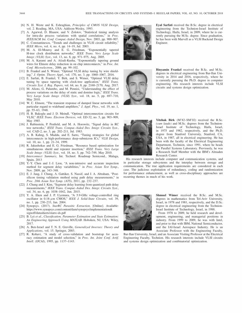
Eyal Sarfati received the B.Sc. degree in electricalengineering from the Technion-Israel Institute ofTechnology, Haifa, Israel, in 2009, where he is cur-rently pursuing the M.Sc. degree. Since graduation,he has been with Marvell as a VLSI Backend DesignEngineer.
Binyamin Frankel received the B.Sc. and M.Sc.degrees in electrical engineering from Bar-Ilan Uni-versity in 2014 and 2016, respectively, where heis currently pursuing the Ph.D. degree in computerengineering. His research interests include VLSIcircuits and systems design optimization.
Yitzhak Birk (M’82–SM’02) received the B.Sc.(cum laude) and M.Sc. degrees from the Technion-Israel Institute of Technology, Haifa, Israel,in 1975 and 1982, respectively, and the Ph.D.degree from Stanford University, Stanford, CA,USA, in 1987, all in electrical engineering. He hasbeen with the faculty of the Electrical EngineeringDepartment, Technion, since 1991, where he headsthe Parallel Systems Laboratory. Previously, he wasa Research Staff Member with the IBM’s AlmadenResearch Center.
His research interests include computer and communication systems, andin particular storage subsystems and the interplay between storage andcommunication. The true application requirements are considered in eachcase. The judicious exploitation of redundancy, coding and randomizationfor performance enhancement, as well as cross-disciplinary approaches arerecurring themes in much of his work.
Shmuel Wimer received the B.Sc. and M.Sc.degrees in mathematics from Tel-Aviv University,Israel, in 1978 and 1981, respectively, and the D.Sc.degree in electrical engineering from the Technion-Israel Institute of Technology, Israel, in 1988.
From 1978 to 2009, he held research and devel-opment, engineering, and managerial positions inindustry. From 1999 to 2009, he was with Intel,and prior to that with IBM, National Semiconductor,and the IAI-Israel Aerospace Industry. He is anAssociate Professor with the Engineering Faculty,
Bar-Ilan University, Israel, and an Associate Visiting Professor at the ElectricalEngineering Faculty, Technion. His research interests include VLSI circuitsand systems design optimization and combinatorial optimization.


![Lect1 Introduction [호환 모드]tera.yonsei.ac.kr/class/2012_2_2/lecture/Introduction.pdf · Interconnect bottleneck ! (ITRS Roadmap 2009) Channel length: 250nm Interconnect delay](https://static.fdocuments.in/doc/165x107/5fb2865e51e929058d7518ca/lect1-introduction-eeoetera-interconnect-bottleneck-itrs-roadmap.jpg)


![Interconnect Topology Optimizationeda.ee.ucla.edu/ECE902_pd/bak/routing.pdf · Steiner Elmore Routing Tree(SERT) Heuristic [Boese-Kahng-Robins, DAC’93] Use Elmore Delay Model directly](https://static.fdocuments.in/doc/165x107/5fccf671cefd5166337abf39/interconnect-topology-steiner-elmore-routing-treesert-heuristic-boese-kahng-robins.jpg)


