
Accurate Coupling-centric Timing Analysis …downloads.hindawi.com/journals/vlsi/2002/263927.pdf ·...
15
Accurate Coupling-centric Timing Analysis Incorporating Temporal and Functional Isolation RAVISHANKAR ARUNACHALAM a, *, RONALD DESHAWN BLANTON b , † and LAWRENCE T. PILEGGI b , ‡ a IBM Corporation, Mail Stop 904-6F015, 11400 Burnett Road, Austin, TX 78758, USA; b Department of Electrical and Computer Engineering, Carnegie Mellon University, 5000 Forbes Avenue, Pittsburgh, PA 15213, USA (Received 15 March 2001; Revised 30 January 2002) Neighboring line switching can contribute to a large portion of the delay of a line for today’s deep submicron designs. The impact of this switching on delay is usually estimated by scaling the coupling capacitances (often by a factor of 2) and modeling them as grounded. This simple approach has been shown to be overly pessimistic in some cases, while somewhat optimistic in others. Apart from the delay modeling inaccuracies, the temporal and functional isolation of the aggressors can contribute to the pessimism. This paper introduces TACO, a timing analysis approach that addresses both these issues. TACO captures the provably worst-and best-case delays as a function of the timing-window inputs to the gates. We then present a comprehensive ATPG-based approach that uses functional information to identify valid interactions between coupled lines. Our algorithm accounts for glitches on aggressors that can be caused by static and dynamic hazards in the circuit. Results on industrial examples and benchmark circuits show the value of our approach. Keywords: Timing analysis; Coupling; Logic information; Worst-case delay; Aggressor; Crosstalk INTRODUCTION Analyzing the impact of crosstalk on delay is critical for present day deep submicron circuits. When a coupled line switches in the opposite direction, the signal delay increases and when it switches in the same direction, the delay decreases. The affected line is referred to as the victim and the affecting line as the aggressor. A common technique used to compute worst-case delay (WCD) of the victim is to scale the coupling capacitances by a “scaling factor” of 2 and model them as grounded. While being overly pessimistic in some cases, this 2 £ approach has also been shown to underestimate the actual WCD in others [1], which is unacceptable. Moreover, this approach does not generalize to resistive interconnect, and it ignores signal switching times and the relative strengths of drivers. An accurate delay model that accounts for coupling must be able to address these issues. An upper bound of 3X for the scaling factor is presented in Refs. [7,13], under certain assumptions. The delay modeling problem forms only a subset of the problems posed by crosstalk to static timing analysis (STA). In order to impact the victim’s delay, an aggressor has to switch simultaneously with the victim. There are two reasons why coupled lines may not switch together— temporal isolation and functional isolation. In STA, timing characteristics are usually specified by arrival time windows, which represent the earliest and latest times that a signal can undergo a transition (either rising or falling). It is possible that a victim and an aggressor have arrival time windows that do not overlap, which implies that they cannot switch together. Functional isolation, on the other hand arises due to the logical relationships between gates. If the logic dictates, for example, that the victim and aggressor can never switch in opposite directions in the same clock cycle, then we have a “false coupling interaction.” Ignoring temporal and functional isolation can lead to highly pessimistic results in STA. In order to determine whether an aggressor and victim are temporally isolated, it is necessary to determine their ISSN 1065-514X print/ISSN 1563-5171 online q 2002 Taylor & Francis Ltd DOI: 10.1080/1065514021000012228 *Corresponding author. Tel.: þ 1-512-838-9454. Fax: þ 1-512-838-4036. E-mail: [email protected] † Tel.: þ 1-412-268-2987. Fax: þ1-412-268-6774. E-mail: [email protected] ‡ Tel./Fax: þ1-412-268-6774. E-mail: [email protected] VLSI Design, 2002 Vol. 15 (3), pp. 605–618
-
Upload
hoangkhanh -
Category
Documents
-
view
221 -
download
0
Transcript of Accurate Coupling-centric Timing Analysis …downloads.hindawi.com/journals/vlsi/2002/263927.pdf ·...
Accurate Coupling-centric Timing Analysis IncorporatingTemporal and Functional Isolation
RAVISHANKAR ARUNACHALAMa,*, RONALD DESHAWN BLANTONb,† and LAWRENCE T. PILEGGIb,‡
aIBM Corporation, Mail Stop 904-6F015, 11400 Burnett Road, Austin, TX 78758, USA; bDepartment of Electrical and Computer Engineering, CarnegieMellon University, 5000 Forbes Avenue, Pittsburgh, PA 15213, USA
(Received 15 March 2001; Revised 30 January 2002)
Neighboring line switching can contribute to a large portion of the delay of a line for today’s deepsubmicron designs. The impact of this switching on delay is usually estimated by scaling the couplingcapacitances (often by a factor of 2) and modeling them as grounded. This simple approach has beenshown to be overly pessimistic in some cases, while somewhat optimistic in others. Apart from thedelay modeling inaccuracies, the temporal and functional isolation of the aggressors can contribute tothe pessimism. This paper introduces TACO, a timing analysis approach that addresses both theseissues. TACO captures the provably worst-and best-case delays as a function of the timing-windowinputs to the gates. We then present a comprehensive ATPG-based approach that uses functionalinformation to identify valid interactions between coupled lines. Our algorithm accounts for glitches onaggressors that can be caused by static and dynamic hazards in the circuit. Results on industrialexamples and benchmark circuits show the value of our approach.
Keywords: Timing analysis; Coupling; Logic information; Worst-case delay; Aggressor; Crosstalk
INTRODUCTION
Analyzing the impact of crosstalk on delay is critical for
present day deep submicron circuits. When a coupled line
switches in the opposite direction, the signal delay
increases and when it switches in the same direction, the
delay decreases. The affected line is referred to as the
victim and the affecting line as the aggressor. A common
technique used to compute worst-case delay (WCD) of the
victim is to scale the coupling capacitances by a “scaling
factor” of 2 and model them as grounded. While being
overly pessimistic in some cases, this 2 £ approach
has also been shown to underestimate the actual WCD
in others [1], which is unacceptable. Moreover, this
approach does not generalize to resistive interconnect, and
it ignores signal switching times and the relative strengths
of drivers. An accurate delay model that accounts for
coupling must be able to address these issues. An upper
bound of 3X for the scaling factor is presented in Refs.
[7,13], under certain assumptions.
The delay modeling problem forms only a subset of the
problems posed by crosstalk to static timing analysis
(STA). In order to impact the victim’s delay, an aggressor
has to switch simultaneously with the victim. There are
two reasons why coupled lines may not switch together—
temporal isolation and functional isolation. In STA, timing
characteristics are usually specified by arrival time
windows, which represent the earliest and latest times
that a signal can undergo a transition (either rising or
falling). It is possible that a victim and an aggressor have
arrival time windows that do not overlap, which implies
that they cannot switch together. Functional isolation, on
the other hand arises due to the logical relationships
between gates. If the logic dictates, for example, that the
victim and aggressor can never switch in opposite
directions in the same clock cycle, then we have a “false
coupling interaction.” Ignoring temporal and functional
isolation can lead to highly pessimistic results in STA.
In order to determine whether an aggressor and victim
are temporally isolated, it is necessary to determine their
ISSN 1065-514X print/ISSN 1563-5171 online q 2002 Taylor & Francis Ltd
DOI: 10.1080/1065514021000012228
*Corresponding author. Tel.: þ1-512-838-9454. Fax: þ1-512-838-4036. E-mail: [email protected]†Tel.: þ1-412-268-2987. Fax: þ1-412-268-6774. E-mail: [email protected]‡Tel./Fax: þ1-412-268-6774. E-mail: [email protected]
VLSI Design, 2002 Vol. 15 (3), pp. 605–618
switching windows first, but these in turn depend on the
delays. Hence, we have a chicken-egg problem where the
delays due to coupling and the switching windows that
specify the arrival times are interdependent. The problem
only gets compounded when multiple aggressors are
involved. An iterative approach is presented in Ref. [6]
and a non-iterative scheduling algorithm is presented in
Ref. [11], but the delay model used is not accurate in either
case.
In this paper, we present TACO, a crosstalk-centric
timing analysis approach capable of handling coupling
effects. In contrast to the scaling approach, TACO uses an
accurate gate-delay engine to compute gate-delays in the
presence of coupling. We use the model presented in Ref.
[3] to determine WCD due to switching aggressors. We
overcome the chicken–egg problem by starting with a
worst case assumption for the switching windows. Under
this assumption, the delay engine produces a pessimistic
delay bound if the timing windows of the aggressors are
not known a priori. The pessimism incurred is removed in
subsequent iterations, in a provably convergent manner.
Most importantly, we provide bounds on the delays and
arrival times, which is very important in the context of
STA.
It is important to determine the impact of functional
isolation, even at the cost of extra CPU time, since it is
unpredictable and largely design-dependent. A related
problem encountered in STA is the well known false-path
problem, which has been extensively researched. How-
ever, the problem of functional relationships of coupled
signals is different in nature and has been addressed only
recently for the noise problem [5]. In this paper, we
present a comprehensive methodology to identify valid
interactions between coupled lines, including a thorough
analysis of glitches that can be caused by potential
hazards. We use an ATPG approach with a six-valued
algebra that includes static and dynamic hazards. Results
are shown for benchmark circuits to consider the
importance of modeling functional information to reduce
the conservatism of most coupled delay models.
The rest of the paper is organized as follows. The
second section describes the coupled delay model that we
use and the aggressor alignment methodology to compute
WCD. We formulate the coupled timing analysis problem
in the third section, and describe the TACO approach. In
the fourth section, we describe our ATPG approach for
identifying functional isolation, and give static and
dynamic sensitization criteria for valid coupling inter-
actions. Conclusions and future work are presented in the
fifth section.
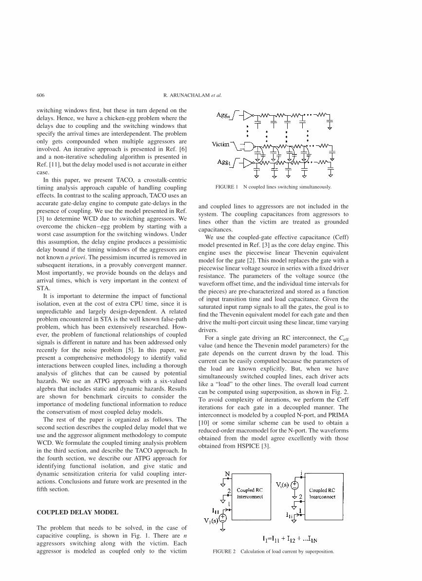
COUPLED DELAY MODEL
The problem that needs to be solved, in the case of
capacitive coupling, is shown in Fig. 1. There are n
aggressors switching along with the victim. Each
aggressor is modeled as coupled only to the victim
and coupled lines to aggressors are not included in the
system. The coupling capacitances from aggressors to
lines other than the victim are treated as grounded
capacitances.
We use the coupled-gate effective capacitance (Ceff)
model presented in Ref. [3] as the core delay engine. This
engine uses the piecewise linear Thevenin equivalent
model for the gate [2]. This model replaces the gate with a
piecewise linear voltage source in series with a fixed driver
resistance. The parameters of the voltage source (the
waveform offset time, and the individual time intervals for
the pieces) are pre-characterized and stored as a function
of input transition time and load capacitance. Given the
saturated input ramp signals to all the gates, the goal is to
find the Thevenin equivalent model for each gate and then
drive the multi-port circuit using these linear, time varying
drivers.
For a single gate driving an RC interconnect, the Ceff
value (and hence the Thevenin model parameters) for the
gate depends on the current drawn by the load. This
current can be easily computed because the parameters of
the load are known explicitly. But, when we have
simultaneously switched coupled lines, each driver acts
like a “load” to the other lines. The overall load current
can be computed using superposition, as shown in Fig. 2.
To avoid complexity of iterations, we perform the Ceff
iterations for each gate in a decoupled manner. The
interconnect is modeled by a coupled N-port, and PRIMA
[10] or some similar scheme can be used to obtain a
reduced-order macromodel for the N-port. The waveforms
obtained from the model agree excellently with those
obtained from HSPICE [3].
FIGURE 2 Calculation of load current by superposition.
FIGURE 1 N coupled lines switching simultaneously.
R. ARUNACHALAM et al.606
For computing best and worst case delays due to
aggressor switching, it is necessary to align the aggressors
with respect to the victim. This is performed as follows:
first the noise waveform is computed, and the peak value
of the noise Vp is found. This waveform is then aligned
such that the peak occurs when the victim value is
Vdd/2-Vp (for a falling victim), so as to just cause the
victim to reach Vdd/2 again. The waveforms can be
superposed within an iteration due to the linearized nature
of the gate models used. This alignment process is
explained in greater detail in Ref. [3].
TACO
The key ideas behind TACO can be stated as follows:
i) Perform STA such that the timing characteristics at
aggressors can be used to determine if it can switch
with the victim.
ii) If it can, determine the switching time of the
aggressor such that it has maximum impact on the
victim and bound the delays and arrival times.
We first define the terminology that will be used to
describe our approach.
Input–output delay: This is defined with respect to a
particular input node and fanout node of a gate, and is the
time difference between the 50% point of the signal at
the input and the 50% point of the signal at the fanout
node.
Best-case delay(BCD ): The input–output delay com-
puted under the condition that the time at which the fanout
node reaches the 50% point is minimized.
Worst-case delay: The input–output delay computed
under the condition that the time at which the fanout node
reaches the 50% point is maximized.
Aggressor net: A net that has “significant” coupling
capacitance to the victim net so as to be able to influence
the input–output delay of the victim gate. The criterion for
coupling capacitance being “significant” is discussed in
the “Pruning of aggressors” section.
Aligned aggressor: An aggressor is said to be an aligned
aggressor with respect to a particular victim, if the
switching window of the aggressor is such that it can
affect to the BCD/WCD of the victim.
Early/Late arrival times (EAT/LAT ): The EATs and
LATs for fanout node j of a gate with n inputs are defined
as follows:
EATj ¼i¼1;2...nMinðEATinput i þ BCDinput i!fanout jÞ ð1Þ
LATj ¼i¼1;2...nMaxðLATinput i þ WCDinput i!fanout jÞ ð2Þ
It must be noted that the EAT and LAT at the output can
be determined by different inputs to the gate. The arrival
times as given by Eqs. (1) and (2) are those obtained when
performing block-based analysis. We choose block-based
analysis for TACO because the arrival times at a node are
then independent of the path propagated. To determine
whether the aggressor can switch with the victim, we have
to use the arrival time windows at the aggressor. In a path-
based analysis, we would not be able to conclude anything
from the arrival time windows at the aggressor. The arrival
times at the aggressor may not overlap with the victim’s
switching when the signal is propagated along a particular
path, but may overlap for some other path. Since our goal
is to obtain bounds on the delays and arrival times at the
victim, we choose a block-oriented approach. We use the
breadth-first search, whereby a gate in a particular level in
the logic is processed only after all gates in the previous
levels have been processed. If the arrival time windows are
set for all inputs of a victim gate, then this gate is pushed
into a FIFO queue called the propagate frontier, which
maintains the list of gates that are to be processed.
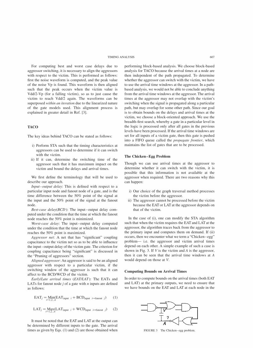
The Chicken–Egg Problem
Though we can use arrival times at the aggressor to
determine whether it can switch with the victim, it is
possible that this information is not available at the
aggressor when required. There are two reasons why this
can happen:
i) Our choice of the graph traversal method processes
the victim before the aggressor.
ii) The aggressor cannot be processed before the victim
because the EAT or LAT at the aggressor depends on
that of the victim.
In the case of (i), one can modify the STA algorithm
such that when the victim requires the EAT and LAT at the
aggressor, the algorithm traces back from the aggressor to
the primary input and computes them on demand. If (ii)
occurs, then we encounter what we term a “Chicken–egg”
problem— i.e. the aggressor and victim arrival times
depend on each other. A simple example of such a case is
shown in Fig. 3. If V is the victim and A is the aggressor,
then it can be seen that the arrival time windows at A
would depend on those at V.
Computing Bounds on Arrival Times
In order to compute bounds on the arrival times (both EAT
and LAT) at the primary outputs, we need to ensure that
we have bounds on the EAT and LAT at each node in the
FIGURE 3 The Chicken–egg problem.
TIMING ANALYSIS 607
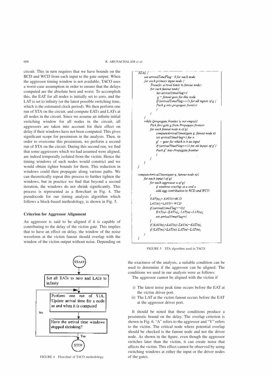
circuit. This in turn requires that we have bounds on the
BCD and WCD from each input to the gate output. When
the aggressor timing window is not available, TACO uses
a worst-case assumption in order to ensure that the delays
computed are the absolute best and worst. To accomplish
this, the EAT for all nodes is initially set to zero, and the
LAT is set to infinity (or the latest possible switching time,
which is the estimated clock period). We then perform one
run of STA on the circuit, and compute EATs and LATs at
all nodes in the circuit. Since we assume an infinite initial
switching window for all nodes in the circuit, all
aggressors are taken into account for their effect on
delay if their windows have not been computed. This gives
significant scope for pessimism in the analysis. Then, in
order to overcome this pessimism, we perform a second
run of STA on the circuit. During this second run, we find
that some aggressors which we had assumed were aligned,
are indeed temporally isolated from the victim. Hence the
timing windows of such nodes would constrict and we
would obtain tighter bounds for them. This reduction in
windows could then propagate along various paths. We
can theoretically repeat this process to further tighten the
windows, but in practice we find that beyond a second
iteration, the windows do not shrink significantly. This
process is represented as a flowchart in Fig. 4. The
pseudocode for our timing analysis algorithm which
follows a block-based methodology, is shown in Fig. 5.
Criterion for Aggressor Alignment
An aggressor is said to be aligned if it is capable of
contributing to the delay of the victim gate. This implies
that to have an effect on delay, the window of the noise
waveform at the victim fanout should overlap with the
window of the victim output without noise. Depending on
the exactness of the analysis, a suitable condition can be
used to determine if the aggressor can be aligned. The
conditions we used in our analysis were as follows:
The aggressor cannot be aligned with the victim if
i) The latest noise peak time occurs before the EAT at
the victim driver port.
ii) The LAT at the victim fanout occurs before the EAT
at the aggressor driver port.
It should be noted that these conditions produce a
pessimistic bound on the delay. The overlap criterion is
shown in Fig. 6. “A” refers to the aggressor and “V” refers
to the victim. The critical node where potential overlap
should be checked is the fanout node and not the driver
node. As shown in the figure, even though the aggressor
switches later than the victim, it can create noise that
affects the victim. This effect cannot be observed by using
switching windows at either the input or the driver nodes
of the gates.FIGURE 4 Flowchart of TACO methodology.
FIGURE 5 STA algorithm used in TACO.
R. ARUNACHALAM et al.608
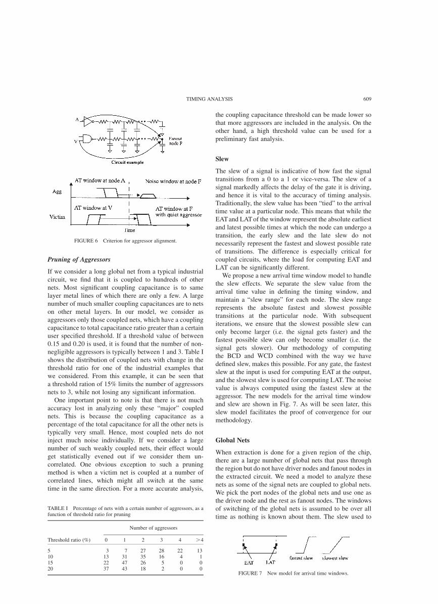
Pruning of Aggressors
If we consider a long global net from a typical industrial
circuit, we find that it is coupled to hundreds of other
nets. Most significant coupling capacitance is to same
layer metal lines of which there are only a few. A large
number of much smaller coupling capacitances are to nets
on other metal layers. In our model, we consider as
aggressors only those coupled nets, which have a coupling
capacitance to total capacitance ratio greater than a certain
user specified threshold. If a threshold value of between
0.15 and 0.20 is used, it is found that the number of non-
negligible aggressors is typically between 1 and 3. Table I
shows the distribution of coupled nets with change in the
threshold ratio for one of the industrial examples that
we considered. From this example, it can be seen that
a threshold ration of 15% limits the number of aggressors
nets to 3, while not losing any significant information.
One important point to note is that there is not much
accuracy lost in analyzing only these “major” coupled
nets. This is because the coupling capacitance as a
percentage of the total capacitance for all the other nets is
typically very small. Hence, most coupled nets do not
inject much noise individually. If we consider a large
number of such weakly coupled nets, their effect would
get statistically evened out if we consider them un-
correlated. One obvious exception to such a pruning
method is when a victim net is coupled at a number of
correlated lines, which might all switch at the same
time in the same direction. For a more accurate analysis,
the coupling capacitance threshold can be made lower so
that more aggressors are included in the analysis. On the
other hand, a high threshold value can be used for a
preliminary fast analysis.
Slew
The slew of a signal is indicative of how fast the signal
transitions from a 0 to a 1 or vice-versa. The slew of a
signal markedly affects the delay of the gate it is driving,
and hence it is vital to the accuracy of timing analysis.
Traditionally, the slew value has been “tied” to the arrival
time value at a particular node. This means that while the
EAT and LAT of the window represent the absolute earliest
and latest possible times at which the node can undergo a
transition, the early slew and the late slew do not
necessarily represent the fastest and slowest possible rate
of transitions. The difference is especially critical for
coupled circuits, where the load for computing EAT and
LAT can be significantly different.
We propose a new arrival time window model to handle
the slew effects. We separate the slew value from the
arrival time value in defining the timing window, and
maintain a “slew range” for each node. The slew range
represents the absolute fastest and slowest possible
transitions at the particular node. With subsequent
iterations, we ensure that the slowest possible slew can
only become larger (i.e. the signal gets faster) and the
fastest possible slew can only become smaller (i.e. the
signal gets slower). Our methodology of computing
the BCD and WCD combined with the way we have
defined slew, makes this possible. For any gate, the fastest
slew at the input is used for computing EAT at the output,
and the slowest slew is used for computing LAT. The noise
value is always computed using the fastest slew at the
aggressor. The new models for the arrival time window
and slew are shown in Fig. 7. As will be seen later, this
slew model facilitates the proof of convergence for our
methodology.
Global Nets
When extraction is done for a given region of the chip,
there are a large number of global nets that pass through
the region but do not have driver nodes and fanout nodes in
the extracted circuit. We need a model to analyze these
nets as some of the signal nets are coupled to global nets.
We pick the port nodes of the global nets and use one as
the driver node and the rest as fanout nodes. The windows
of switching of the global nets is assumed to be over all
time as nothing is known about them. The slew used to
FIGURE 6 Criterion for aggressor alignment.
TABLE I Percentage of nets with a certain number of aggressors, as afunction of threshold ratio for pruning
Threshold ratio (%)
Number of aggressors
0 1 2 3 4 .4
5 3 7 27 28 22 1310 13 31 35 16 4 115 22 47 26 5 0 020 37 43 18 2 0 0
FIGURE 7 New model for arrival time windows.
TIMING ANALYSIS 609
drive the global net should typically be the fastest possible
slew in the circuit. This will facilitate computation of a
bound for the windows as they are primarily used as
aggressors. A standard driver resistance is used for the
Thevenin model of the global nets.
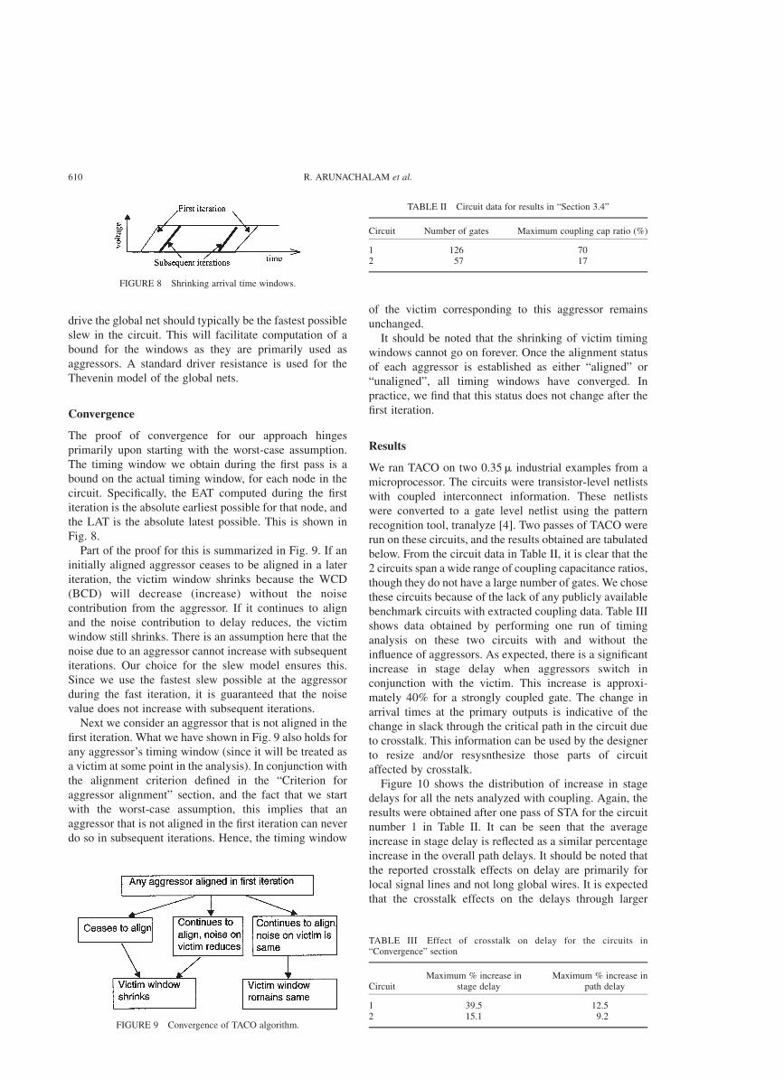
Convergence
The proof of convergence for our approach hinges
primarily upon starting with the worst-case assumption.
The timing window we obtain during the first pass is a
bound on the actual timing window, for each node in the
circuit. Specifically, the EAT computed during the first
iteration is the absolute earliest possible for that node, and
the LAT is the absolute latest possible. This is shown in
Fig. 8.
Part of the proof for this is summarized in Fig. 9. If an
initially aligned aggressor ceases to be aligned in a later
iteration, the victim window shrinks because the WCD
(BCD) will decrease (increase) without the noise
contribution from the aggressor. If it continues to align
and the noise contribution to delay reduces, the victim
window still shrinks. There is an assumption here that the
noise due to an aggressor cannot increase with subsequent
iterations. Our choice for the slew model ensures this.
Since we use the fastest slew possible at the aggressor
during the fast iteration, it is guaranteed that the noise
value does not increase with subsequent iterations.
Next we consider an aggressor that is not aligned in the
first iteration. What we have shown in Fig. 9 also holds for
any aggressor’s timing window (since it will be treated as
a victim at some point in the analysis). In conjunction with
the alignment criterion defined in the “Criterion for
aggressor alignment” section, and the fact that we start
with the worst-case assumption, this implies that an
aggressor that is not aligned in the first iteration can never
do so in subsequent iterations. Hence, the timing window
of the victim corresponding to this aggressor remains
unchanged.
It should be noted that the shrinking of victim timing
windows cannot go on forever. Once the alignment status
of each aggressor is established as either “aligned” or
“unaligned”, all timing windows have converged. In
practice, we find that this status does not change after the
first iteration.
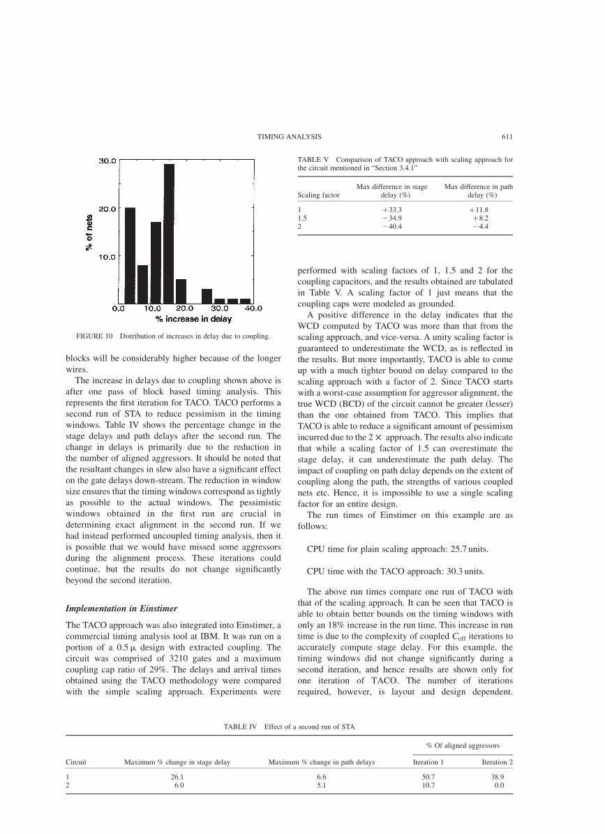
Results
We ran TACO on two 0.35m industrial examples from a
microprocessor. The circuits were transistor-level netlists
with coupled interconnect information. These netlists
were converted to a gate level netlist using the pattern
recognition tool, tranalyze [4]. Two passes of TACO were
run on these circuits, and the results obtained are tabulated
below. From the circuit data in Table II, it is clear that the
2 circuits span a wide range of coupling capacitance ratios,
though they do not have a large number of gates. We chose
these circuits because of the lack of any publicly available
benchmark circuits with extracted coupling data. Table III
shows data obtained by performing one run of timing
analysis on these two circuits with and without the
influence of aggressors. As expected, there is a significant
increase in stage delay when aggressors switch in
conjunction with the victim. This increase is approxi-
mately 40% for a strongly coupled gate. The change in
arrival times at the primary outputs is indicative of the
change in slack through the critical path in the circuit due
to crosstalk. This information can be used by the designer
to resize and/or resysnthesize those parts of circuit
affected by crosstalk.
Figure 10 shows the distribution of increase in stage
delays for all the nets analyzed with coupling. Again, the
results were obtained after one pass of STA for the circuit
number 1 in Table II. It can be seen that the average
increase in stage delay is reflected as a similar percentage
increase in the overall path delays. It should be noted that
the reported crosstalk effects on delay are primarily for
local signal lines and not long global wires. It is expected
that the crosstalk effects on the delays through larger
TABLE II Circuit data for results in “Section 3.4”
Circuit Number of gates Maximum coupling cap ratio (%)
1 126 702 57 17
FIGURE 8 Shrinking arrival time windows.
FIGURE 9 Convergence of TACO algorithm.
TABLE III Effect of crosstalk on delay for the circuits in“Convergence” section
CircuitMaximum % increase in
stage delayMaximum % increase in
path delay
1 39.5 12.52 15.1 9.2
R. ARUNACHALAM et al.610
blocks will be considerably higher because of the longer
wires.
The increase in delays due to coupling shown above is
after one pass of block based timing analysis. This
represents the first iteration for TACO. TACO performs a
second run of STA to reduce pessimism in the timing
windows. Table IV shows the percentage change in the
stage delays and path delays after the second run. The
change in delays is primarily due to the reduction in
the number of aligned aggressors. It should be noted that
the resultant changes in slew also have a significant effect
on the gate delays down-stream. The reduction in window
size ensures that the timing windows correspond as tightly
as possible to the actual windows. The pessimistic
windows obtained in the first run are crucial in
determining exact alignment in the second run. If we
had instead performed uncoupled timing analysis, then it
is possible that we would have missed some aggressors
during the alignment process. These iterations could
continue, but the results do not change significantly
beyond the second iteration.
Implementation in Einstimer
The TACO approach was also integrated into Einstimer, a
commercial timing analysis tool at IBM. It was run on a
portion of a 0.5m design with extracted coupling. The
circuit was comprised of 3210 gates and a maximum
coupling cap ratio of 29%. The delays and arrival times
obtained using the TACO methodology were compared
with the simple scaling approach. Experiments were
performed with scaling factors of 1, 1.5 and 2 for the
coupling capacitors, and the results obtained are tabulated
in Table V. A scaling factor of 1 just means that the
coupling caps were modeled as grounded.
A positive difference in the delay indicates that the
WCD computed by TACO was more than that from the
scaling approach, and vice-versa. A unity scaling factor is
guaranteed to underestimate the WCD, as is reflected in
the results. But more importantly, TACO is able to come
up with a much tighter bound on delay compared to the
scaling approach with a factor of 2. Since TACO starts
with a worst-case assumption for aggressor alignment, the
true WCD (BCD) of the circuit cannot be greater (lesser)
than the one obtained from TACO. This implies that
TACO is able to reduce a significant amount of pessimism
incurred due to the 2 £ approach. The results also indicate
that while a scaling factor of 1.5 can overestimate the
stage delay, it can underestimate the path delay. The
impact of coupling on path delay depends on the extent of
coupling along the path, the strengths of various coupled
nets etc. Hence, it is impossible to use a single scaling
factor for an entire design.
The run times of Einstimer on this example are as
follows:
CPU time for plain scaling approach: 25.7 units.
CPU time with the TACO approach: 30.3 units.
The above run times compare one run of TACO with
that of the scaling approach. It can be seen that TACO is
able to obtain better bounds on the timing windows with
only an 18% increase in the run time. This increase in run
time is due to the complexity of coupled Ceff iterations to
accurately compute stage delay. For this example, the
timing windows did not change significantly during a
second iteration, and hence results are shown only for
one iteration of TACO. The number of iterations
required, however, is layout and design dependent.
FIGURE 10 Distribution of increases in delay due to coupling.
TABLE V Comparison of TACO approach with scaling approach forthe circuit mentioned in “Section 3.4.1”
Scaling factorMax difference in stage
delay (%)Max difference in path
delay (%)
1 þ33.3 þ11.81.5 234.9 þ8.22 240.4 24.4
TABLE IV Effect of a second run of STA
Circuit Maximum % change in stage delay Maximum % change in path delays
% Of aligned aggressors
Iteration 1 Iteration 2
1 26.1 6.6 50.7 38.92 6.0 5.1 10.7 0.0
TIMING ANALYSIS 611
Every extra iteration of TACO involves a complete run
of timing analysis, and hence will increase the run time.
TACO offers designers the flexibility to stop the
iterations if significant reduction in pessimism is not
expected. It should be noted that even the first iteration of
TACO gives results that are more accurate than the
scaling approach, with the 18% increase in run time.
Hence, the methodology can be easily scaled to large-
sized circuits.
FUNCTIONAL ISOLATION
Problem Formulation
We limit the problem of finding false interactions to
combinational circuits only. Sequential circuits can be
separated at flip-flops and the flip-flop outputs can be
treated as primary inputs, as is usually done in STA.
Coupling interactions between the victim and aggressors
can be categorized into two types: delay-increase and
delay-decrease. The delay-increase interaction occurs
when all aggressors switch in the opposite direction to that
of the victim, and vice-versa. We will not deal with the
noise problem caused by coupling.
We denote a rising transition on a line by " and a
falling transition by # . Since we are dealing with
transitions on signal lines rather than just single values,
there are two different input vectors for which the circuit
needs to be analyzed. Note that this implies that we use
the 2-vector transition mode [14] for analysis. This is
different from the floating mode analyses in Ref. [15]
whereby the initial state of the circuit is assumed to be
known. We denote the two vectors by v1, v2 and the clock
period of the circuit by T. s(t; v1, v2) represents the “state”
of a particular signal, t time units after vector v2 is
applied. Though the state is defined after v2 is applied, it
depends on the value of the signal before v2, and hence v1.
Possible values of s(t; v1, v2) are 0, 1, " , # for
0 , t , T and 0, 1 for t ¼ 0 and t ¼ T:We assume the
circuit reaches steady state after v1 is applied and before
v2 is applied.
Definition A system S is defined as a set of lines with
one victim V and n aggressors A1;A2. . .An that are coupled
to it.
S ¼ {V ;A1;A2. . .An}
Definition The delay–increase interaction of a system
S ¼ {V;A1;A2; . . .An} is valid only if:
’v1; v2; t0; 0 , t0 , T ;
Vðt0; v1; v2Þ ¼"; Aiðt0; v1; v2Þ ¼#; i ¼ 1; 2. . .n ð3Þ
or
Vðt0; v1; v2Þ ¼#; Aiðt0; v1; v2Þ ¼"; i ¼ 1; 2. . .n ð4Þ
Similarly, the delay–decrease interaction is valid only
if:
’v1; v2; t0; 0 , t0 , T ;
Vðt0; v1; v2Þ ¼"; Aiðt0; v1; v2Þ ¼"; i ¼ 1; 2. . .n ð5Þ
or
Vðt0; v1; v2Þ ¼#; Aiðt0; v1; v2Þ ¼#; i ¼ 1; 2. . .n ð6Þ
For all aggressors to contribute to the delay of the
victim, the corresponding coupling interaction must be
valid. It should be noted that an interaction which is
invalid for a system with one victim and n aggressors can
be valid for a subsystem that includes only a subset of the
aggressors.
It is not necessary to compute the value of each signal
for each time point t [ [0,T ] in order to determine
whether a coupling interaction is valid. The arrival time
windows can be used to determine whether a t0 can
possibly exist. This process of temporal pruning identifies
those systems where the aggressors and victim can
“potentially” switch simultaneously. It should be noted
that STA can never ensure that they switch together, since
it performs an input pattern independent analysis. We can
now remove the simultaneity constraint from the
conditions given above, which means the conditions (3)
and (4) can be relaxed to:
’v1; v2; t0; ti; 0 , t0 , T ; 0 , ti , T ; i ¼ 1; 2. . .n
Vðt0; v1; v2Þ ¼"; Aiðti; v1; v2Þ ¼#; i ¼ 1; 2. . .n ð7Þ
or
Vðt0; v1; v2Þ ¼#; Aiðti; v1; v2Þ ¼"; i ¼ 1; 2. . .n ð8Þ
The functional and temporal aspects of the problem are
separated from each other in this manner. Even though we
remove the simultaneity constraint, we only incur an error
on the conservative side. If it so happens that interactions
classified as valid under the above conditions cannot take
place in reality, then the victim delays are overestimated.
This is acceptable because we are only interested in
bounds for the delays and arrival times in STA. Our goal in
identifying false interactions is to still bound the actual
delays while ensuring that the bounds are as tight as
possible.
Static Vs. Dynamic Sensitization
Definition The delay-increase coupling interaction of a
system is statically sensitizable if:
’ v1; v2 :
Vð0; v1; v2Þ ¼ 0; VðT ; v1; v2Þ ¼ 1;
Aið0; v1; v2Þ ¼ 1; AiðT; v1; v2Þ ¼ 0; i ¼ 1; 2. . .n ð9Þ
R. ARUNACHALAM et al.612
or
Vð0; v1; v2Þ ¼ 1; VðT ; v1; v2Þ ¼ 0;
Aið0; v1; v2Þ ¼ 0; AiðT; v1; v2Þ ¼ 1; i ¼ 1; 2. . .n ð10Þ
A similar definition holds for the delay–decrease
interaction.
Static sensitizability implies that there exist input
vectors v1 and v2 that cause transitions on each of the
victim and aggressor lines. An interaction that is not
statically sensitizable is “statically unsensitizable”.
Theorem 1 If Eq. (9) holds for an input vector pair
(v1, v2), then Eq. (10) holds for the vector pair (v2, v1).
This will reduce the number of cases that must be
analyzed by half for each system.
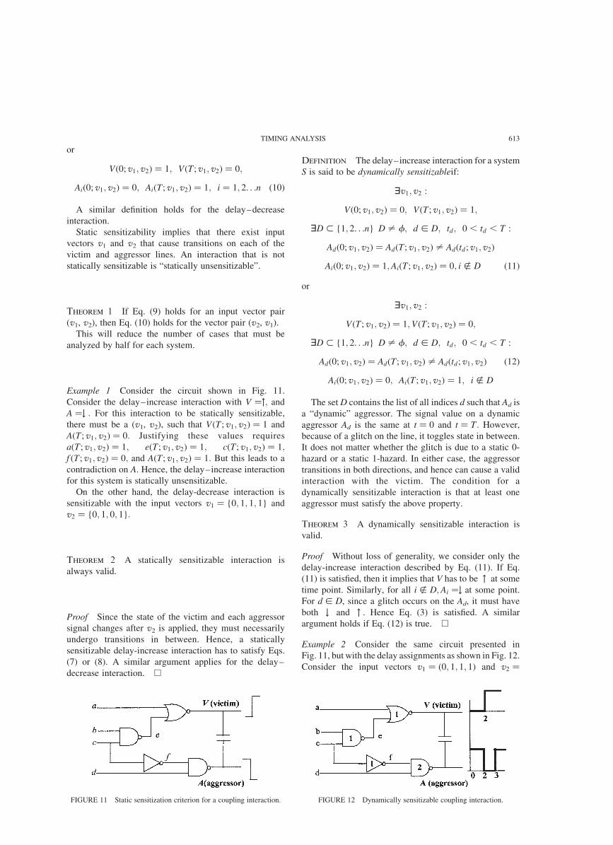
Example 1 Consider the circuit shown in Fig. 11.
Consider the delay–increase interaction with V ¼"; and
A ¼# : For this interaction to be statically sensitizable,
there must be a (v1, v2), such that VðT ; v1; v2Þ ¼ 1 and
AðT ; v1; v2Þ ¼ 0: Justifying these values requires
aðT; v1; v2Þ ¼ 1; eðT; v1; v2Þ ¼ 1; cðT; v1; v2Þ ¼ 1;f ðT; v1; v2Þ ¼ 0; and AðT ; v1; v2Þ ¼ 1: But this leads to a
contradiction on A. Hence, the delay–increase interaction
for this system is statically unsensitizable.
On the other hand, the delay-decrease interaction is
sensitizable with the input vectors v1 ¼ {0; 1; 1; 1} and
v2 ¼ {0; 1; 0; 1}:
Theorem 2 A statically sensitizable interaction is
always valid.
Proof Since the state of the victim and each aggressor
signal changes after v2 is applied, they must necessarily
undergo transitions in between. Hence, a statically
sensitizable delay-increase interaction has to satisfy Eqs.
(7) or (8). A similar argument applies for the delay–
decrease interaction. A
Definition The delay–increase interaction for a system
S is said to be dynamically sensitizableif:
’v1; v2 :
Vð0; v1; v2Þ ¼ 0; VðT ; v1; v2Þ ¼ 1;
’D , {1; 2. . .n} D – f; d [ D; td; 0 , td , T :
Adð0; v1; v2Þ ¼ AdðT ; v1; v2Þ – Adðtd; v1; v2Þ
Aið0; v1; v2Þ ¼ 1;AiðT; v1; v2Þ ¼ 0; i � D ð11Þ
or
’v1; v2 :
VðT ; v1; v2Þ ¼ 1;VðT ; v1; v2Þ ¼ 0;
’D , {1; 2. . .n} D – f; d [ D; td; 0 , td , T :
Adð0; v1; v2Þ ¼ AdðT; v1; v2Þ – Adðtd; v1; v2Þ ð12Þ
Aið0; v1; v2Þ ¼ 0; AiðT ; v1; v2Þ ¼ 1; i � D
The set D contains the list of all indices d such that Ad is
a “dynamic” aggressor. The signal value on a dynamic
aggressor Ad is the same at t ¼ 0 and t ¼ T : However,
because of a glitch on the line, it toggles state in between.
It does not matter whether the glitch is due to a static 0-
hazard or a static 1-hazard. In either case, the aggressor
transitions in both directions, and hence can cause a valid
interaction with the victim. The condition for a
dynamically sensitizable interaction is that at least one
aggressor must satisfy the above property.
Theorem 3 A dynamically sensitizable interaction is
valid.
Proof Without loss of generality, we consider only the
delay-increase interaction described by Eq. (11). If Eq.
(11) is satisfied, then it implies that V has to be " at some
time point. Similarly, for all i � D;Ai ¼# at some point.
For d [ D, since a glitch occurs on the Ad, it must have
both # and " . Hence Eq. (3) is satisfied. A similar
argument holds if Eq. (12) is true. A
Example 2 Consider the same circuit presented in
Fig. 11, but with the delay assignments as shown in Fig. 12.
Consider the input vectors v1 ¼ ð0; 1; 1; 1Þ and v2 ¼
FIGURE 11 Static sensitization criterion for a coupling interaction. FIGURE 12 Dynamically sensitizable coupling interaction.
TIMING ANALYSIS 613
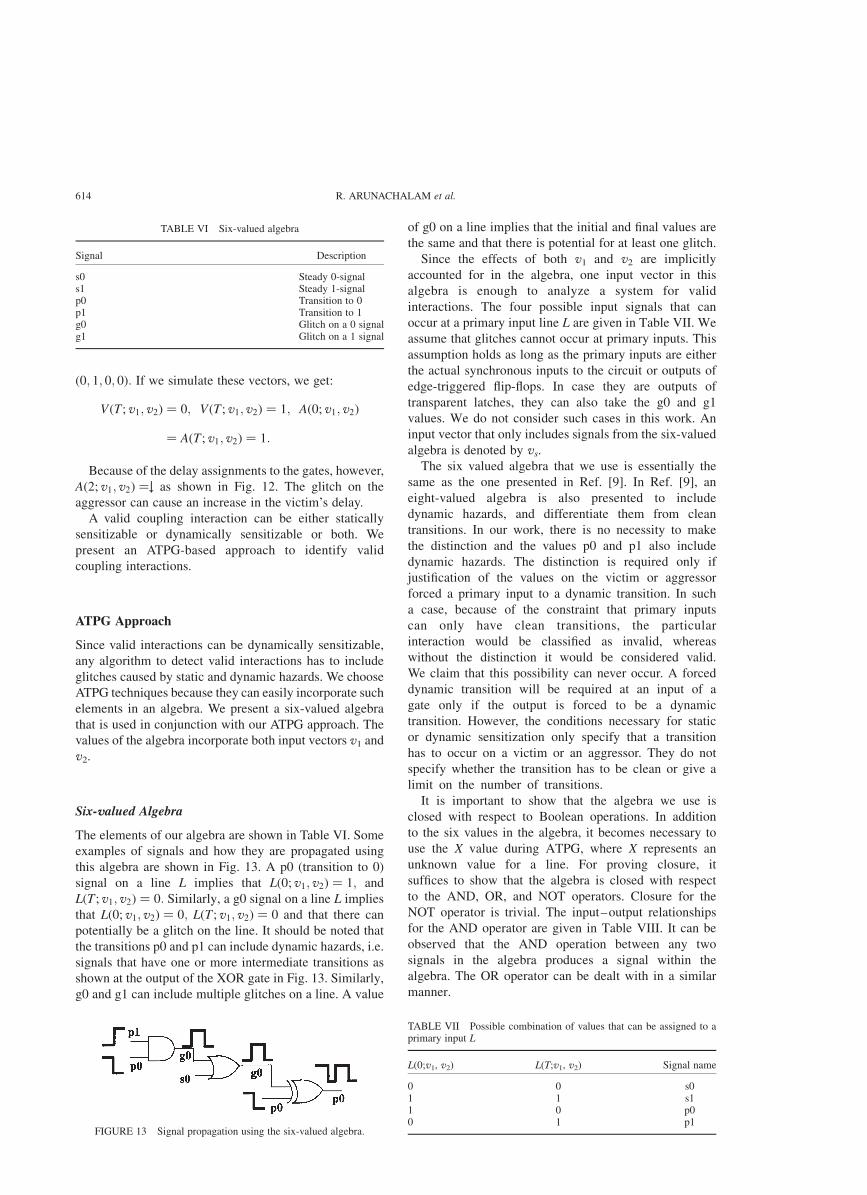
ð0; 1; 0; 0Þ: If we simulate these vectors, we get:
VðT; v1; v2Þ ¼ 0; VðT ; v1; v2Þ ¼ 1; Að0; v1; v2Þ
¼ AðT ; v1; v2Þ ¼ 1:
Because of the delay assignments to the gates, however,
Að2; v1; v2Þ ¼# as shown in Fig. 12. The glitch on the
aggressor can cause an increase in the victim’s delay.
A valid coupling interaction can be either statically
sensitizable or dynamically sensitizable or both. We
present an ATPG-based approach to identify valid
coupling interactions.
ATPG Approach
Since valid interactions can be dynamically sensitizable,
any algorithm to detect valid interactions has to include
glitches caused by static and dynamic hazards. We choose
ATPG techniques because they can easily incorporate such
elements in an algebra. We present a six-valued algebra
that is used in conjunction with our ATPG approach. The
values of the algebra incorporate both input vectors v1 and
v2.
Six-valued Algebra
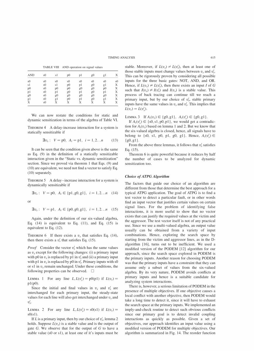
The elements of our algebra are shown in Table VI. Some
examples of signals and how they are propagated using
this algebra are shown in Fig. 13. A p0 (transition to 0)
signal on a line L implies that Lð0; v1; v2Þ ¼ 1; and
LðT ; v1; v2Þ ¼ 0: Similarly, a g0 signal on a line L implies
that Lð0; v1; v2Þ ¼ 0; LðT ; v1; v2Þ ¼ 0 and that there can
potentially be a glitch on the line. It should be noted that
the transitions p0 and p1 can include dynamic hazards, i.e.
signals that have one or more intermediate transitions as
shown at the output of the XOR gate in Fig. 13. Similarly,
g0 and g1 can include multiple glitches on a line. A value
of g0 on a line implies that the initial and final values are
the same and that there is potential for at least one glitch.
Since the effects of both v1 and v2 are implicitly
accounted for in the algebra, one input vector in this
algebra is enough to analyze a system for valid
interactions. The four possible input signals that can
occur at a primary input line L are given in Table VII. We
assume that glitches cannot occur at primary inputs. This
assumption holds as long as the primary inputs are either
the actual synchronous inputs to the circuit or outputs of
edge-triggered flip-flops. In case they are outputs of
transparent latches, they can also take the g0 and g1
values. We do not consider such cases in this work. An
input vector that only includes signals from the six-valued
algebra is denoted by vs.
The six valued algebra that we use is essentially the
same as the one presented in Ref. [9]. In Ref. [9], an
eight-valued algebra is also presented to include
dynamic hazards, and differentiate them from clean
transitions. In our work, there is no necessity to make
the distinction and the values p0 and p1 also include
dynamic hazards. The distinction is required only if
justification of the values on the victim or aggressor
forced a primary input to a dynamic transition. In such
a case, because of the constraint that primary inputs
can only have clean transitions, the particular
interaction would be classified as invalid, whereas
without the distinction it would be considered valid.
We claim that this possibility can never occur. A forced
dynamic transition will be required at an input of a
gate only if the output is forced to be a dynamic
transition. However, the conditions necessary for static
or dynamic sensitization only specify that a transition
has to occur on a victim or an aggressor. They do not
specify whether the transition has to be clean or give a
limit on the number of transitions.
It is important to show that the algebra we use is
closed with respect to Boolean operations. In addition
to the six values in the algebra, it becomes necessary to
use the X value during ATPG, where X represents an
unknown value for a line. For proving closure, it
suffices to show that the algebra is closed with respect
to the AND, OR, and NOT operators. Closure for the
NOT operator is trivial. The input–output relationships
for the AND operator are given in Table VIII. It can be
observed that the AND operation between any two
signals in the algebra produces a signal within the
algebra. The OR operator can be dealt with in a similar
manner.
TABLE VI Six-valued algebra
Signal Description
s0 Steady 0-signals1 Steady 1-signalp0 Transition to 0p1 Transition to 1g0 Glitch on a 0 signalg1 Glitch on a 1 signal
FIGURE 13 Signal propagation using the six-valued algebra.
TABLE VII Possible combination of values that can be assigned to aprimary input L
L(0;v1, v2) L(T;v1, v2) Signal name
0 0 s01 1 s11 0 p00 1 p1
R. ARUNACHALAM et al.614
We can now restate the conditions for static and
dynamic sensitization in terms of the algebra of Table VI.
Theorem 4 A delay-increase interaction for a system is
statically sensitizable if
’vs : V ¼ p0; Ai ¼ p1; i ¼ 1; 2. . .n ð13Þ
It can be seen that the condition given above is the same
as Eq. (9) in the definition of a statically sensitizable
interaction given in the “Static vs. dynamic sensitization”
section. Since we proved via theorem 1 that Eqs. (9) and
(10) are equivalent, we need not find a vector to satisfy Eq.
(10) separately.
Theorem 5 A delay–increase interaction for a system is
dynamically sensitizable if
’vs : V ¼ p0; Ai [ {p1; g0; g1}; i ¼ 1; 2. . .n ð14Þ
or
’vs : V ¼ p1; Ai [ {p0; g0; g1}; i ¼ 1; 2. . .n ð15Þ
Again, under the definition of our six-valued algebra,
Eq. (14) is equivalent to Eq. (11), and Eq. (15) is
equivalent to Eq. (12).
Theorem 6 If there exists a vs that satisfies Eq. (14),
then there exists a v0s that satisfies Eq. (15).
Proof Consider the vector v0s which has the same values
as vs except for the following changes: (i) a primary input
with p0 in vs is replaced by p1 in v0s and (ii) a primary input
with p1 in vs is replaced by p0 in v0s. Primary inputs with s0
or s1 in vs remain unchanged. Under these conditions, the
following properties can be observed. A
Lemma 1 For any line L; Lðv0sÞ ¼ p0ðp1Þ if LðvsÞ ¼
p1ðp0Þ:Since the initial and final values in vs and v0
s are
interchanged for each primary input, the steady-state
values for each line will also get interchanged under vs and
v0s.
Lemma 2 For any line L; Lðv0sÞ ¼ s0ðs1Þ if LðvsÞ ¼
s0ðs1Þ:If L is a primary input, then by our choice of v0
s, lemma 2
holds. Suppose L(vs) is a stable value and is the output of
gate G. We observe that for the output of G to have a
stable value (s0 or s1), at least one of it’s inputs must be
stable. Moreover, if L(vs) – L(v0s), then at least one of
those stable inputs must change values between vs and v0s.
This can be rigorously proven by considering all possible
inputs for the three basic gates: NOT, AND, and OR.
Hence, if L(vs) – L(v0s), then there exists an input I of G
such that I(vs) – I(v0s) and I(vs) is a stable value. This
process of back tracing can continue till we reach a
primary input, but by our choice of v0s, stable primary
inputs have the same values in vs and v0s. This implies that
LðvsÞ ¼ Lðv0sÞ:
Lemma 3 If AiðvsÞ [ {g0; g1}; Aiðv0sÞ [ {g0; g1}:
If Aiðv0sÞ [ {s0; s1; p0; p1}; we would get a contradic-
tion for Ai(vs) based on lemma 1 and 2. But we know that
the six-valued algebra is closed, hence, all signals have to
belong to {s0, s1, p0, p1, g0, g1}. Hence, Aiðv0sÞ [
{g0; g1}:From the above three lemmas, it follows that v0
s satisfies
Eq. (15).
Theorem 6 is quite powerful because it reduces by half
the number of cases to be analyzed for dynamic
sensitization too.
Choice of ATPG Algorithm
The factors that guide our choice of an algorithm are
different from those that determine the best approach for a
typical ATPG application. The goal of ATPG is to find a
test vector to detect a particular fault, or in other words
find an input vector that justifies certain values on certain
signal lines. For the problem of identifying false
interactions, it is more useful to show that no vector
exists that can justify the required values at the victim and
the aggressor. The test vector itself is not of any practical
use. Since we use a multi-valued algebra, an output value
usually can be obtained from a variety of input
combinations. Hence, exploring the search space by
starting from the victim and aggressor lines, as in the D-
algorithm [16], turns out to be inefficient. We used a
modified version of the PODEM [12] algorithm for our
approach, since the search space explored in PODEM is
the primary inputs. Another reason for choosing PODEM
was that the primary inputs have a constraint that they can
assume only a subset of values from the six-valued
algebra. By its very nature, PODEM avoids conflicts at
primary inputs and hence is a suitable candidate for
analyzing system interactions.
There is, however, a serious limitation of PODEM in the
presence of multiple objectives. If one objective causes a
local conflict with another objective, then PODEM would
take a long time to detect it, since it will have to exhaust
the search space at the primary inputs. We implemented an
imply-and-check routine to detect such obvious conflicts
since our primary goal is to detect invalid coupling
interactions as quickly as possible. Given a set of
objectives, our approach identifies an input value using a
modified version of PODEM for multiple objectives. Our
algorithm is summarized in Fig. 14. The reorder function
TABLE VIII AND operation on signal values
AND s0 s1 p0 p1 g0 g1 X
s0 s0 s0 s0 s0 s0 s0 s0s1 s0 s1 p0 p1 g0 g1 Xp0 s0 p0 p0 g0 g0 p0 Xp1 s0 p1 g0 p1 g0 p1 Xg0 s0 g0 g0 g0 g0 g0 Xg1 s0 g1 p0 p1 g0 g1 XX s0 X X X X X X
TIMING ANALYSIS 615
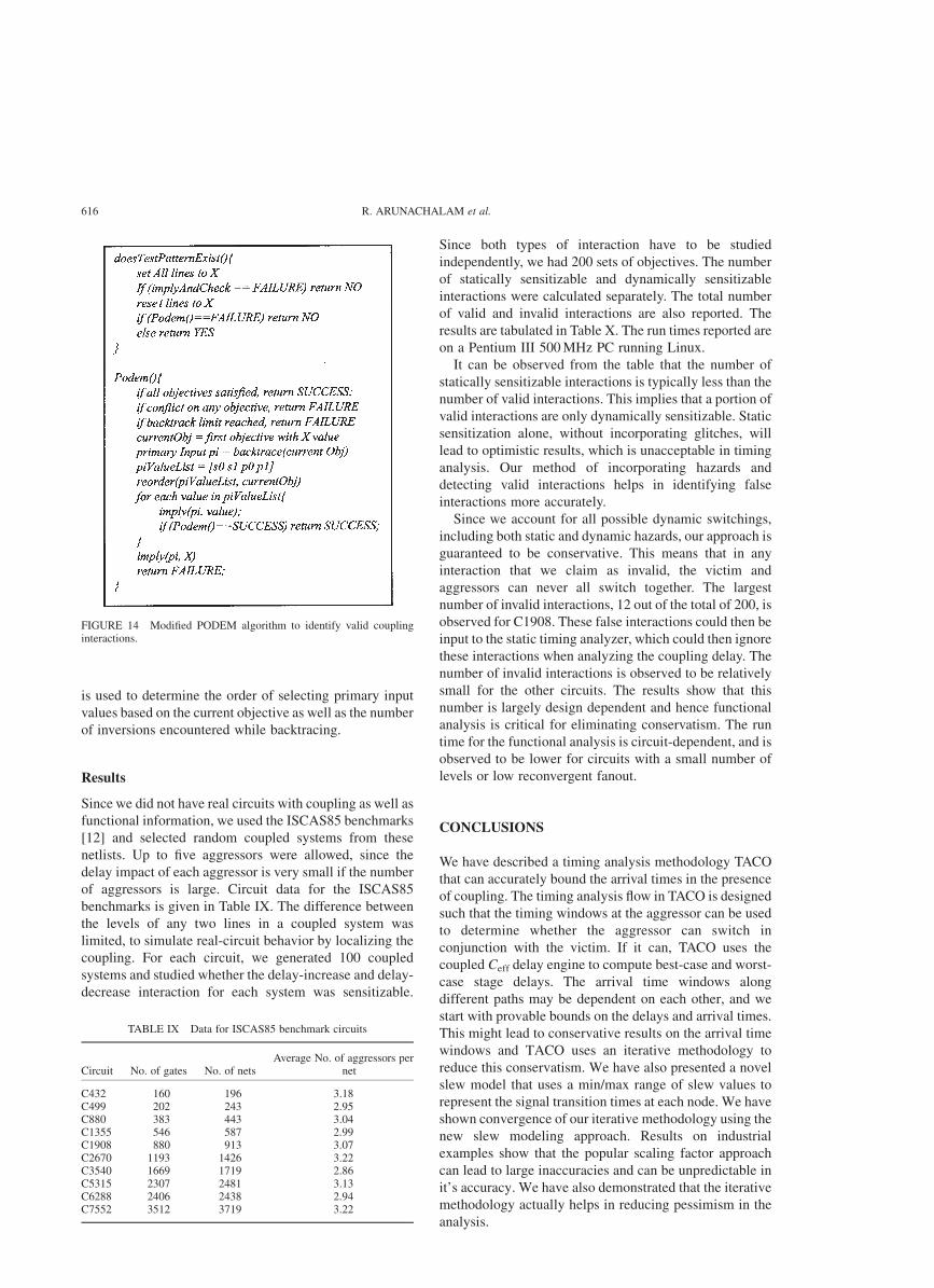
is used to determine the order of selecting primary input
values based on the current objective as well as the number
of inversions encountered while backtracing.
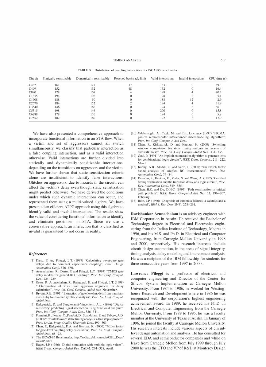
Results
Since we did not have real circuits with coupling as well as
functional information, we used the ISCAS85 benchmarks
[12] and selected random coupled systems from these
netlists. Up to five aggressors were allowed, since the
delay impact of each aggressor is very small if the number
of aggressors is large. Circuit data for the ISCAS85
benchmarks is given in Table IX. The difference between
the levels of any two lines in a coupled system was
limited, to simulate real-circuit behavior by localizing the
coupling. For each circuit, we generated 100 coupled
systems and studied whether the delay-increase and delay-
decrease interaction for each system was sensitizable.
Since both types of interaction have to be studied
independently, we had 200 sets of objectives. The number
of statically sensitizable and dynamically sensitizable
interactions were calculated separately. The total number
of valid and invalid interactions are also reported. The
results are tabulated in Table X. The run times reported are
on a Pentium III 500 MHz PC running Linux.
It can be observed from the table that the number of
statically sensitizable interactions is typically less than the
number of valid interactions. This implies that a portion of
valid interactions are only dynamically sensitizable. Static
sensitization alone, without incorporating glitches, will
lead to optimistic results, which is unacceptable in timing
analysis. Our method of incorporating hazards and
detecting valid interactions helps in identifying false
interactions more accurately.
Since we account for all possible dynamic switchings,
including both static and dynamic hazards, our approach is
guaranteed to be conservative. This means that in any
interaction that we claim as invalid, the victim and
aggressors can never all switch together. The largest
number of invalid interactions, 12 out of the total of 200, is
observed for C1908. These false interactions could then be
input to the static timing analyzer, which could then ignore
these interactions when analyzing the coupling delay. The
number of invalid interactions is observed to be relatively
small for the other circuits. The results show that this
number is largely design dependent and hence functional
analysis is critical for eliminating conservatism. The run
time for the functional analysis is circuit-dependent, and is
observed to be lower for circuits with a small number of
levels or low reconvergent fanout.
CONCLUSIONS
We have described a timing analysis methodology TACO
that can accurately bound the arrival times in the presence
of coupling. The timing analysis flow in TACO is designed
such that the timing windows at the aggressor can be used
to determine whether the aggressor can switch in
conjunction with the victim. If it can, TACO uses the
coupled Ceff delay engine to compute best-case and worst-
case stage delays. The arrival time windows along
different paths may be dependent on each other, and we
start with provable bounds on the delays and arrival times.
This might lead to conservative results on the arrival time
windows and TACO uses an iterative methodology to
reduce this conservatism. We have also presented a novel
slew model that uses a min/max range of slew values to
represent the signal transition times at each node. We have
shown convergence of our iterative methodology using the
new slew modeling approach. Results on industrial
examples show that the popular scaling factor approach
can lead to large inaccuracies and can be unpredictable in
it’s accuracy. We have also demonstrated that the iterative
methodology actually helps in reducing pessimism in the
analysis.
FIGURE 14 Modified PODEM algorithm to identify valid couplinginteractions.
TABLE IX Data for ISCAS85 benchmark circuits
Circuit No. of gates No. of netsAverage No. of aggressors per
net
C432 160 196 3.18C499 202 243 2.95C880 383 443 3.04C1355 546 587 2.99C1908 880 913 3.07C2670 1193 1426 3.22C3540 1669 1719 2.86C5315 2307 2481 3.13C6288 2406 2438 2.94C7552 3512 3719 3.22
R. ARUNACHALAM et al.616
We have also presented a comprehensive approach to
incorporate functional information in an STA flow. When
a victim and set of aggressors cannot all switch
simultaneously, we classify that particular interaction as
a false coupling interaction, and as a valid interaction
otherwise. Valid interactions are further divided into
statically and dynamically sensitizable interactions,
depending on the transitions on aggressors and the victim.
We have further shown that static sensitization criteria
alone are insufficient to identify false interactions.
Glitches on aggressors, due to hazards in the circuit, can
affect the victim’s delay even though static sensitization
might predict otherwise. We have derived the conditions
under which such dynamic interactions can occur, and
represented them using a multi-valued algebra. We have
presented an efficient ATPG approach using this algebra to
identify valid and invalid interactions. The results show
the value of considering functional information to identify
and eliminate pessimism in STA. Since we use a
conservative approach, an interaction that is classified as
invalid is guaranteed to not occur in reality.
References
[1] Dartu, F. and Pileggi, L.T. (1997) “Calculating worst-case gatedelays due to dominant capacitance coupling”, Proc. DesignAutomation Conf., 576–580.
[2] Arunachalam, R., Dartu, F. and Pileggi, L.T. (1997) “CMOS gatedelay models for general RLC loading”, Proc. Int. Conf. Comput.Des., 224–229.
[3] Gross, P., Arunachalam, R., Rajagopal, K. and Pileggi, L.T. (1998)“Determination of worst case aggressor alignment for delaycalculation”, Proc. Int. Conf. Comput.-Aided Des. November.
[4] Bryant, R.E. (1991) “Extraction of gate level models from transistorcircuits by four-valued symbolic analysis”, Proc. Int. Conf. Comput.Aided Des..
[5] Kirkpatrick, D. and Sangiovanni-Vincentelli, A.L. (1996) “Digitalsensitivity: predicting signal interaction using functional analysis”,Proc. Int. Conf. Comput.-Aided Des., 536–541.
[6] Franzini, B., Forzan, C., Pandini, D., Scandolara, P. and Fabbro, A.D.(2000) “Crosstalk aware static timing analysis: a two step approach”,Proc. 1st Int. Symp. Quality Electronic Des., 499–503.
[7] Chen, P., Kirkpatrick, D.A. and Keutzer, K. (2000) “Miller factorfor gate-level coupling delay calculation”, Proc. Int. Conf. Comput.-Aided Des., 68–73.
[8] The ISCAS-85 Benchmarks. http://zodiac.cbl.ncsu.edu/CBL_Docs/iscas85.html
[9] Hayes, J.P. (1986) “Digital simulation with multiple logic values”,IEEE Trans. Comput.-Aided Des. CAD-5, 274–328, April.
[10] Odabasioglu, A., Celik, M. and T.P., Lawrence (1997) “PRIMA:passive reduced-order inter-connect macromodeling algorithm”,Proc. Int. Conf. Comput.-Aided Des..
[11] Chen, P., Kirkpatrick, D. and Keutzer, K. (2000) “Switchingwindow computation for static timing analysis in presence ofcrosstalk noise”, Proc. Int. Conf. Comput.-Aided Des., 331–336.
[12] Goel, P. (1991) “An implicit enumeration algorithm to generate testsfor combinational logic circuits”, IEEE Trans. Comput., 211–222,March.
[13] Kahng, A.B., Muddu, S. and Sarto, E. (2000) “On switch factorbased analysis of coupled RC interconnects”, Proc. Des.Automation Conf., 79–84.
[14] Devadas, S., Keutzer, K., Malik, S. and Wang, A. (1992) “Certifiedtiming verification and the transition delay of a logic circuit”, Proc.Des. Automation Conf., 549–555.
[15] Chen, H.C. and Du, D.H.C. (1993) “Path sensitization in criticalpath problem”, IEEE Trans. Comput.-Aided Des. 12, 196–207,February.
[16] Roth, J.P. (1966) “Diagnosis of automata failures: a calculus and amethod”, IBM J. Res. Dev. 10(4), 278–291.
Ravishankar Arunachalam is an advisory engineer with
IBM Corporation in Austin. He received the Bachelor of
Technology degree in Electrical and Electronics engin-
eering from the Indian Institute of Technology, Madras in
1996, and his M.S. and Ph.D. in Electrical and Computer
Engineering, from Carnegie Mellon University in 1998
and 2000, respectively. His research interests include
circuit design automation, in the areas of signal integrity,
timing analysis, delay modeling and interconnect analysis.
He was a recipient of the IBM fellowship for students for
three consecutive years from 1997 to 2000.
Lawrence Pileggi is a professor of electrical and
computer engineering and Director of the Center for
Silicon System Implementation at Carnegie Mellon
University. From 1984 to 1986, he worked for Westing-
house Research and Development where in 1986 he was
recognized with the corporation’s highest engineering
achievement award. In 1989, he received his Ph.D. in
Electrical and Computer Engineering from the Carnegie
Mellon University. From 1989 to 1995, he was a faculty
member at the University of Texas at Austin. In January of
1996, he joined the faculty at Carnegie Mellon University.
His research interests include various aspects of circuit-
level design automation and analysis. He has consulted for
several EDA and semiconductor companies and while on
leave from Carnegie Mellon from July 1999 through July
2000 he was the CTO and VP of R&D at Monterey Design
TABLE X Distribution of coupling interactions for ISCAS85 benchmarks
Circuit Statically sensitizable Dynamically sensitizable Reached backtrack limit Valid interactions Invalid interactions CPU time (s)
C432 161 127 17 183 0 89.3C499 152 152 48 152 0 16.4C880 178 168 4 188 4 40.3C1355 194 196 0 198 2 5.1C1908 188 50 0 188 12 2.9C2670 184 152 2 194 4 31.9C3540 146 166 0 194 6 186C5315 198 146 0 200 0 15.8C6288 178 176 0 194 6 5.8C7552 182 160 0 192 8 17.9
TIMING ANALYSIS 617
Systems. He received the Best CAD Transactions Paper
Award in 1991 for “Asymptotic Waveform Evaluation
(AWE),” and again in 1999 for “Passive Reduced-order
Interconnect Macromodeling Algorithm (PRIMA).” He
received a Presidential Young Investigator Award from the
National Science Foundation in 1991. In 1991 and in
1999, he received the Semiconductor Research Corpor-
ation Technical Excellence Award. In 1993, he received an
Invention Award from the SRC and subsequently a U.S.
Patent for the RICE simulation tool. In 1994, he received
The University of Texas Parent’s Association Centennial
Teaching Fellowship for excellence in undergraduate
instruction. In 1995, he received a Faculty Partnership
Award from IBM. He is a co-author of “Electronic Circuit
and System Simulation Methods,” McGraw-Hill, 1995. He
has published over 125 refereed conference and journal
papers and holds five U.S. patents.
Shawn Blanton is an associate professor in the
Department of Electrical and Computer Engineering at
Carnegie Mellon University where he is a member of the
Center for Silicon Systems Implementation (CSSI). He
received the Bachelor’s degree in engineering from Calvin
College in 1987, a Master’s degree in Electrical
Engineering in 1989 from the University of Arizona and
a Ph.D. degree in Computer Science and Engineering from
the University of Michigan, Ann Arbor in 1995. His
research interests include the computer-aided design of
VLSI circuits and systems; fault-tolerant computing and
diagnosis; verification and testing; and computer archi-
tecture. He has worked on the design and test of integrated
systems with General Motors Research Laboratories,
AT&T Bell Laboratories, Intel and Motorola. Dr Blanton
is the recipient of National Science Foundation Career
Award and is a member of IEEE and ACM.
R. ARUNACHALAM et al.618

International Journal of
AerospaceEngineeringHindawi Publishing Corporationhttp://www.hindawi.com Volume 2010
RoboticsJournal of
Hindawi Publishing Corporationhttp://www.hindawi.com Volume 2014
Hindawi Publishing Corporationhttp://www.hindawi.com Volume 2014
Active and Passive Electronic Components
Control Scienceand Engineering
Journal of
Hindawi Publishing Corporationhttp://www.hindawi.com Volume 2014
International Journal of
RotatingMachinery
Hindawi Publishing Corporationhttp://www.hindawi.com Volume 2014
Hindawi Publishing Corporation http://www.hindawi.com
Journal ofEngineeringVolume 2014
Submit your manuscripts athttp://www.hindawi.com
VLSI Design
Hindawi Publishing Corporationhttp://www.hindawi.com Volume 2014
Hindawi Publishing Corporationhttp://www.hindawi.com Volume 2014
Shock and Vibration
Hindawi Publishing Corporationhttp://www.hindawi.com Volume 2014
Civil EngineeringAdvances in
Acoustics and VibrationAdvances in
Hindawi Publishing Corporationhttp://www.hindawi.com Volume 2014
Hindawi Publishing Corporationhttp://www.hindawi.com Volume 2014
Electrical and Computer Engineering
Journal of
Advances inOptoElectronics
Hindawi Publishing Corporation http://www.hindawi.com
Volume 2014
The Scientific World JournalHindawi Publishing Corporation http://www.hindawi.com Volume 2014
SensorsJournal of
Hindawi Publishing Corporationhttp://www.hindawi.com Volume 2014
Modelling & Simulation in EngineeringHindawi Publishing Corporation http://www.hindawi.com Volume 2014
Hindawi Publishing Corporationhttp://www.hindawi.com Volume 2014
Chemical EngineeringInternational Journal of Antennas and
Propagation
International Journal of
Hindawi Publishing Corporationhttp://www.hindawi.com Volume 2014
Hindawi Publishing Corporationhttp://www.hindawi.com Volume 2014
Navigation and Observation
International Journal of
Hindawi Publishing Corporationhttp://www.hindawi.com Volume 2014
DistributedSensor Networks
International Journal of