ABSTRACT QU, JUN. Development of Cylindrical Wire ... · The cylindrical wire Electrical Discharge...
127
ABSTRACT QU, JUN. Development of Cylindrical Wire Electrical Discharge Machining Process and Investigation of Surface Integrity and Mechanical Property of EDM Surface Layers. (Under the direction of Albert J. Shih) The cylindrical wire Electrical Discharge Machining (EDM) process was developed to generate precise cylindrical forms on hard, difficult-to-machine materials. A precise, flexible, and corrosion-resistant underwater rotary spindle was designed and added to a conventional two-axis wire EDM machine to enable the generation of free-form cylindrical geometries. A detailed spindle error analysis identified the major source of error at different frequencies. The mathematical models for material removal rate and surface finish were derived. Experimental results indicated that higher maximum material removal rate might be achieved in the cylindrical wire EDM than the 2D wire EDM. Effects of some key process parameters, wire feed rate, pulse on-time and part rotational speed, on the surface finish and roundness are explored. For WC-Co parts, an arithmetic average surface roughness and roundness as low as 0.68 and 1.7 μm, respectively, can be achieved. Surfaces of the cylindrical EDM parts were examined using Scanning Electron Microscopy (SEM) to identify the macro-ridges and craters on the surface. Cross-sections of the EDM parts are examined using the SEM to quantify the recast layer and heat-affected zone under various process parameters. This study also used nanoindentation to investigate the influence of cylindrical wire EDM process on the mechanical properties of WC-Co composite. Multiple indents were conducted on the cross-section of the recast layer, heat-affected zone, and bulk material. The SEM micrographs were used to correlate the individual nano-indent to the measured hardness
Transcript of ABSTRACT QU, JUN. Development of Cylindrical Wire ... · The cylindrical wire Electrical Discharge...

ABSTRACT
QU, JUN. Development of Cylindrical Wire Electrical Discharge Machining Process and Investigation of Surface Integrity and Mechanical Property of EDM Surface Layers. (Under the direction of Albert J. Shih)
The cylindrical wire Electrical Discharge Machining (EDM) process was developed
to generate precise cylindrical forms on hard, difficult-to-machine materials. A precise,
flexible, and corrosion-resistant underwater rotary spindle was designed and added to a
conventional two-axis wire EDM machine to enable the generation of free-form
cylindrical geometries. A detailed spindle error analysis identified the major source of
error at different frequencies. The mathematical models for material removal rate and
surface finish were derived. Experimental results indicated that higher maximum
material removal rate might be achieved in the cylindrical wire EDM than the 2D wire
EDM. Effects of some key process parameters, wire feed rate, pulse on-time and part
rotational speed, on the surface finish and roundness are explored. For WC-Co parts, an
arithmetic average surface roughness and roundness as low as 0.68 and 1.7 µm,
respectively, can be achieved. Surfaces of the cylindrical EDM parts were examined
using Scanning Electron Microscopy (SEM) to identify the macro-ridges and craters on
the surface. Cross-sections of the EDM parts are examined using the SEM to quantify
the recast layer and heat-affected zone under various process parameters. This study also
used nanoindentation to investigate the influence of cylindrical wire EDM process on the
mechanical properties of WC-Co composite. Multiple indents were conducted on the
cross-section of the recast layer, heat-affected zone, and bulk material. The SEM
micrographs were used to correlate the individual nano-indent to the measured hardness
and modulus of elasticity. The experimental results showed that the heat-affected zone
had more compact microstructure less indentation cracking. The recast layer had lower
hardness and modulus of elasticity than the original material and heat-affected zone.
EDS X-ray and X-ray diffraction were used to analyze the material compositions of the
heat-affected zone and recast layer and to understand the effects of wire EDM process on
the machined WC-Co surface. The micro-blasting process has been applied to improve
the surface integrity of the part machined by wire EDM. The surface roughness of WC-
Co parts could be reduced significantly using micro-size SiC abrasives. The surface
finish improvement was also shown by the SEM micrographs of the blasted surfaces and
their cross-sections. The undesired recast layer, which has poor mechanical properties
and irregular features, was eventually removed by micro-blasting. Compressive residual
stress introduced by micro-blasting could increase the surface wear resistance.
Experiments with different process parameters were conduced to study the efficiency and
effectiveness of micro-blasting for surface property control.

DEVELOPMENT OF CYLINDRICAL WIRE ELECTRICAL DISCHARGE MACHINING PROCESS AND INVESTIGATION OF SURFACE INTEGRITY
AND MECHANICAL PROPERTY OF EDM SURFACE LAYERS
by JUN QU
A dissertation submitted to the Graduate Faculty of North Carolina State University
in partial fulfillment of the requirements for the Degree of
Ph.D.
MECHANICAL ENGINEERING
Raleigh, North Carolina
2002
APPROVED BY:

ii
DEDICATION
May this work commemorate my grandmother, who dedicated herself to bringing me
up. Through all life’s sunny and rainy days, I feel you were there, which encouraged me
to head up with smile. I would like to thank you in my heart, and I know you are
listening.
To my family and all my friends I thank you for the past 29 years. I cannot think of
better people to be with through this dance we call life.

iii
BIOGRAPHY
Jun Qu was born in Shenyang, P.R. China. He is the first son of Weihong Qu and
Guifeng Zhao and brother of Gang Qu. Both of his parents are environmental engineers
and dedicate themselves to the research on air pollution and natural sources protection.
In middle school, Jun met Ye Sun, who became his wife 13 years later. They fell in love
in junior (1993) and got married in 1998 at Ames, Iowa. Now their lovely ten-month-old
son, Steven S. Qu, has started to learn walking.
Jun showed his talents on Physics and Mathematics in high school and chose
Precision Instrument Engineering as the major when he enrolled in Tianjin University in
1991. He achieved his Bachelor’s degree and entered the graduate school in 1995.
During his research work, Jun was lucky to get the guidance of Professor Guoxiong
Zhang, one of the most famous scholars in precision engineering in the world.
At the beginning of 1998, Jun came to US and joined Iowa State University. After 18
months research work in CAD/CAM with Dr. Radha Sarma, he got another Master’s
degree in Mechanical Engineering. Jun achieved the Outstanding Paper Award Finalist
from the North American Manufacturing Research Institution of the Society of
Manufacturing Engineers (NAMRI/SME) in 1999.
Jun has spent the last three years pursuing a Doctoral degree in Mechanical
Engineering at NC State University. To be a Ph.D. is one of his dreams from childhood.
Under the guidance of his supervisor Dr. Albert Shih and advisory committee, Jun has
done good research work in Precision Manufacturing and Material Characterization. He
will be graduating in May and start working at Oak Ridge National Laboratory.

iv
ACKNOWLEDGMENTS
I would like to first thank my advisor, Dr. Albert J. Shih. I have learned and improved a lot with your guidance and help in the past three years. Thank you for your efforts, time, and energy and give my best regards to you and your family.
I would like to take this opportunity to thank my advisory committee members, Dr.
Jeffrey Eischen, Dr. John Strenkowski, and Dr. Paul Franzon, for your guidance and help. I would like to thank my parents. Your unfailing support and encouragement have
meant more than what you will ever know. With my heart, I thank you. I would like to thank my wife, Ye Sun. Your love is always the source of my energy. I would also like to give a special thank to my mother-in-law. Without your help on
taking care of my son, I could not fully dedicate myself to the research work in the past twelve months.
Gratefully acknowledge the support by National Science Foundation Grant #9983582
(Dr. K. P. Rajurkar, Program Director). Portion of this research was sponsored by the User program in the High Temperature
Material Lab, Oak Ridge National Lab and the Heavy Vehicle Propulsion Systems Materials Program, Office of Transportation Technologies, US Department of Energy.
Thanks to Everyone at Oak Ridge National Lab who assisted in this research,
especially:
• Dr. Arvid Pasto, for coordinating the involvement of NCSU with ORNL. • Dr. Ray Johnson, for his guidance on this project. • Sam McSpadden Jr., for facilitating the work at HTML, ORNL. • Laura Riester, for doing the Nanoindentation experiments. • Dr. Ronald Ott, for his help during visiting HTML, ORNL. • Dr. Thomas Watkins, for assisting the X-Ray diffraction experiments. • Dr. Edgar Lara-Curzio, for assisting the material characterization. • Tom Geer, for polishing the wire EDM parts. • Dorothy Coffey, for assisting the SEM experiments. • Randy Parten, for assisting the surface roughness and roundness measurement. • Larry Walker, for assisting the SEM and EDX experiments. • Tyler Jenkins, for slicing the wire EDM parts.
Thanks to Darryl Gust of Cummins Technical Center for the design and manufacture
of the underwater spindle.

v
TABLE OF CONTENTS
Page
LIST OF TABLES ............................................................................................................. vii
LIST OF FIGURES ...........................................................................................................viii
1. INTRODUCTION ........................................................................................................ 1
1.1. Background of Electrical Discharge Machining (EDM) ........................................1 1.2. Overview.................................................................................................................6 References ......................................................................................................................8
2. CONCEPT, DESIGN, AND MATERIAL REMOVAL RATE OF CYLINDRICAL WIRE ELECTRICAL DISCHARGE MACHINING..................................................10
2.1. Introduction...........................................................................................................10 2.2. Spindle Design ......................................................................................................12 2.3. Spindle Error Analysis ..........................................................................................13 2.4. Material Removal Rate Modeling.........................................................................15 2.5. Experiment on the Maximum Material Removal Rate .........................................17 2.6. Concluding Remarks.............................................................................................22 References ....................................................................................................................23
3. SURFACE INTEGRITY AND ROUNDNESS OF CYLINDRICAL WIRE ELECTRICAL DISCHARGE MACHINING .............................................................24
3.1. Introduction...........................................................................................................24 3.2. Surface Finish Modeling .......................................................................................26 3.3. Experiments on Surface Finish and Roundness ....................................................29 3.4. SEM Micrographs of EDM Surface and Sub-Surface ..........................................39 3.5. Concluding Remarks.............................................................................................44 References ....................................................................................................................45
4. ANALYTICAL SURFACE ROUGHNESS PARAMETERS OF A THEORETICAL PROFILE CONSISTING OF ELLIPTICAL OR CIRCULAR ARCS........................47
4.1. Introduction...........................................................................................................47 4.2. Closed-from Expressions of Roughness Parameters for a Theoretical Surface
Profile Consisting of Elliptical Arcs.....................................................................49 4.3. Roughness Parameters in Dimensionless Form....................................................54 4.4. Theoretical Surface Profile Consisting of Circular Arcs ......................................59 4.5. Approximate Solutions .........................................................................................60 4.6. Concluding Remarks.............................................................................................66

vi
References ....................................................................................................................67
5. NANOINDENTATION CHARACTERIZATION OF SURFACE LAYERS OF ELECTRICAL DISCHARGE MACHINED WC- CO ................................................70
5.1. Introduction...........................................................................................................70 5.2. Experiment Setup and Sample Preparation...........................................................71 5.3. Experimental Results and Discussion...................................................................73 5.4. Concluding Remarks.............................................................................................83 References ....................................................................................................................84
6. ABRASIVE MICRO - BLASTING OF WIRE ELECTRICAL DISCHARGE MACHINED WC- CO COMPOSITE ..........................................................................87
6.1. Introduction...........................................................................................................87 6.2. Sample Preparation and Experiment Setup ...........................................................91 6.3. Experimental Results and Discussion...................................................................93 6.4. Concluding Remarks...........................................................................................100 References ..................................................................................................................100
7. CONCLUSIONS........................................................................................................103
APPENDICES .................................................................................................................106
Appendix A. Material Removal Rate Modeling in Cylindrical Wire EDM.............107 Appendix B. Derivation of Semi-Axes a and b and Feed f for a Measurement Profile
on the Surface Machined by Flat-End Milling ....................................112 Appendix C. Derivation of the Closed-Form Ra and Rq Using the Parametric Form .............................................................................................................114

vii
LIST OF TABLES
Page
Chapter 2
Table 2.1. Machine setup for the cylindrical wire EDM experiment ..........................18 Table 2.2. MRRmax for the cylindrical wire EDM test with α = 0 and gradually
increasing vf................................................................................................20 Table 2.3. MRRmax for the cylindrical wire EDM test with constant α and vf.............20 Table 2.4. MRRmax for the 2D wire EDM test .............................................................21
Chapter 3
Table 3.1. Machine setup for the Experiments I and II...............................................31 Table 3.2. Material removal rate of Experiments I and II...........................................31 Table 3.3. Surface finish of 2D wire EDM parts in Experiment I ..............................34
Chapter 4
Table 4.1. Error analysis of approximate solutions ....................................................66
Chapter 5
Table 5.1. Hardness and modulus of elasticity of bulk material, heat-affected zone, and recast layer in descending order of the hardness.................................75
Table 5.2. Experimental conditions of the X-ray diffraction measurements ..............82
Chapter 6
Table 6.1. Process parameters of wire EDM rough cut and skim cut .........................91 Table 6.2. Process parameters of Micro-blasting experiments ...................................92

viii
LIST OF FIGURES
Page
Chapter 1
Fig. 1.1. Illustration of the wire EDM process ............................................................2 Fig. 1.2. Four types of gap conditions in EDM ...........................................................3 Fig. 1.3. Evolution of a single spark in the EDM process ...........................................5
Chapter 2
Fig. 2.1. The concept of cylindrical wire EDM process ............................................11 Fig. 2.2. A cylindrical wire EDM part with the same shape as the diesel engine
injector plunger............................................................................................11 Fig. 2.3. Side view of the hybrid bearing underwater spindle ...................................13 Fig. 2.4. Spindle error at 30 rpm rotational speed .....................................................14 Fig. 2.5. Spindle error vs. Rotational speed ...............................................................15 Fig. 2.6. FFT frequency spectrum of the spindle error ..............................................15 Fig. 2.7. Parameters in the free form cylindrical wire EDM process ........................16 Fig. 2.8. Four test configurations to find the maximum material removal rate.........19 Fig. 2.9. Key parameters of the two configurations to find the maximum material
removal rate in cylindrical wire EDM.........................................................20
Chapter 3
Fig. 3.1. Cross-section view of an ideal cylindrical wire EDM surface and the key parameters and coordinate system for mathematical modeling ..................26
Fig. 3.2. The configuration of surface finish experiment ..........................................32 Fig. 3.3. The surface finish and roundness of cylindrical wire EDM parts in
Experiment I with high material removal rate.............................................35 Fig. 3.4. The surface finish and roundness of cylindrical wire EDM parts in
Experiment II with improvements on surface finish and roundness ...........38 Fig. 3.5. SEM micrographs of macro-ridges and ideal arcs on surfaces of brass parts
in Experiment I ............................................................................................40 Fig. 3.6. SEM micrographs of surfaces and cross-sections of carbide parts .............41 Fig. 3.7. SEM micrographs of surfaces and cross-sections of brass samples ............42
Chapter 4
Fig. 4.1. A theoretical surface profile consisting of elliptical arcs ............................50 Fig. 4.2. Dimensionless surface roughness parameters Rt/b, Ra/b, and Rq/b vs. f/a...58 Fig. 4.3. Comparison of closed-form and approximate solutions of surface finish
parameters....................................................................................................65

ix
Chapter 5
Fig. 5.1. MTS Nano-indenterTM II .............................................................................73 Fig. 5.2. Nanoindentation on the cross-section of WC-Co part machined by
cylindrical wire EDM ..................................................................................74 Fig. 5.3. Nanoindentation on the bulk ma terial .........................................................77 Fig. 5.4. Nanoindentation on heat-affected zone .......................................................79 Fig. 5.5. EDS X-Ray analysis of the recast layer ......................................................81 Fig. 5.6. X-Ray diffraction analysis of the recast layer .............................................81 Fig. 5.7. Nanoindentation on the recast layer ............................................................83
Chapter 6
Fig. 6.1. SEM micrographs of the surface and cross-section of a WC-Co part machined by wire EDM...............................................................................88
Fig. 6.2. Micro-blasting on a micro cylindrical wire EDM WC-Co part ..................90 Fig. 6.3. Two sizes of SiC abrasives ..........................................................................92 Fig. 6.4. Erosion wear rate of micro-blasting on wire EDM WC-Co........................94 Fig. 6.5. Surface finish improvement on wire EDM WC-Co using micro-blasting ..97 Fig. 6.6. SEM micrographs of surfaces and cross-sections of the wire EDM rough
cut WC-CO part after micro-blasting using abrasive A at 0.276 MPa air pressure ........................................................................................................97
Fig. 6.7. SEM micrographs of surfaces and cross-sections of the wire EDM rough cut WC-CO part after micro-blasting using abrasive A at 0.138 MPa air pressure ........................................................................................................98
Fig. 6.8. SEM micrographs of surfaces and cross-sections of the wire EDM rough cut WC-CO part after micro-blasting using abrasive B at 0.138 MPa air pressure ........................................................................................................98
Fig. 6.9. SEM micrographs of surfaces and cross-sections of the wire EDM skim cut WC-CO part after micro-blasting using abrasive B at 0.276 MPa air pressure ........................................................................................................99
Fig. 6.10. SEM micrographs of surfaces and cross-sections of the wire EDM skim cut WC-CO part after micro-blasting using abrasive A at 0.276 MPa air pressure ........................................................................................................99
Appendices
Fig. A.1. Free form geometry in cylindrical wire EDM...........................................107 Fig. A.2. Calculation of VII .......................................................................................108 Fig. A.3. Calculation of VIII ......................................................................................110 Fig. B.1. The measurement profile on the surface machined by flat-end milling ....113

Chapter 1 1
CHAPTER 1. INTRODUCTION
1.1. Background of Electrical Discharge Machining (EDM)
In the past decades, EDM technology has gradually evolved and become an
important manufacturing process. EDM is a thermoelectric process that erodes
workpiece material by a series of discrete electrical sparks between the workpiece and
electrode flushed by or immersed in a dielectric fluid. Unlike traditional cutting and
grinding processes which rely on a much harder tool or abrasive material to remove the
softer work-material, the EDM process utilizes electrical sparks or thermal energy to
erode the unwanted work-material and generate the desired shape. The material removal
rate of EDM process mainly depends on the electrical conductivity and melting
temperature of the work-material [1]. A workpiece with higher electrical conductivity
and lower melting temperature can be machined more efficiently. The hardness and
strength of the work-material are no longer the dominating factors that affect the tool
wear and hinder the machining process. This makes EDM particularly suitable for
machining hard, difficult-to-machine materials, such as Metal Matrix Composites
(MMCs). The EDM process has the ability to machine precise, complex, and irregular
shapes with a CNC control system. In addition, the cutting force in the EDM process is
small, which makes it ideal for fabricating parts with miniature features. Ehrfeld et al. [2]
and Michel and Ehrfeld [3] reviewed the application of micro wire EDM in

Chapter 1 2
manufacturing mechatronic micro devices. Kruusing, et al. [4] studied the machining of
micro-magnets. The micro-EDM of silicon has also been well addressed [5,6].
There are two typical types of EDM processes, die-sinking EDM and wire EDM. The
electrode of die-sinking EDM has the reversed shape of the part to be machined, while
wire EDM uses brass wire, ranging from 0.01 to 0.36 mm in diameter, as the electrode.
Figure 1.1(a) illustrates the wire EDM process, a traveling wire eroding a groove in the
workpiece. The close-up view of the gap and electrical sparks between the wire and
workpiece is illustrated in Fig. 1.1(b).
(a) Wire EDM. (b) Close-up view of the gap. Fig. 1.1. Illustration of the wire EDM process.
Four types of gap conditions, open, spark, arc, and short, exist in the EDM process,
as shown in Fig. 1.2 [1]. It can be seen that sparks or effective discharge require some
delay time before the discharge current reaches its nominal value. The arcs, however,
require negligible or zero delay time and occur at a lower breakdown voltage due to
partially deionized dielectric. When the distance between the two electrodes is far
X Y
Traveling wire
Workpiece
Voltage pulses to generate electrical sparks
Traveling wire
Electrical sparks generated in the gap to remove the work-material

Chapter 1 3
enough, an open voltage pulse occurs with no current. A short circuit pulse is the result
of direct contact between the wire electrode and the workpiece. The debris particles in
the gap may form a bridge between two electrodes to create a short circuit. Flushing with
the high pressure deionized water is the way to prevent it. Sparks are the desired gap
condition in EDM. Arcs, which damage the surface finish and dimensional accuracy,
should be avoided. In order to optimize the EDM process, different types of monitoring
and control systems have been developed, such as the ignition delay monitoring system
[7], DDS monitoring system [8], R.F. monitoring system [8], and EDM discharge
parameter monitoring system [10,11].
Fig. 1.2. Four types of gap conditions in EDM [1].
The procedure of a single electrical spark discharge can be illustrated by Fig. 1.3 [12].
The voltage and current charts are shown at the bottom of each illustration. In all the
diagrams, the electrode (anode in this case) is the upper dark-color material and the
Voltage
Current

Chapter 1 4
workpiece is the lower jagged part that is negatively charged. The dielectric fluid in the
machining gap serves as an insulator. First, the electrode moving close to the workpiece
as shown in Fig. 1.3(a). As the potential difference increases between the two surfaces,
the local dielectric fluid breaks down and ions are generated. The electrical field is
strongest at the point where the distance between the two surfaces is minimal. The
electrical spark will occur at that location. Note the voltage has increased, but no current
is flowing because of the presence of the dielectric material.
Next, as shown in Fig. 1.3(b), more and more ions have been generated, making the
insulating properties of the dielectric fluid begin to decrease along a narrow channel at
the point with the strongest electrical field. Voltage reaches its peak, while current is still
zero. Figure 1.3(c) shows that a current starts to be established, causing the voltage to
decrease. A discharge channel begins to form between the electrode and workpiece. The
voltage continues dropping, as shown in Fig. 1.3(d), while the current continues
increasing. Heat builds up rapidly, causing some of the anode, cathode, and dielectric
materials to vaporize.
Figure 1.3(e) depicts the expansion of the discharge channel full of vapor is
constrained by the rush of ions, attracted by the intense electro-magnetic field, toward it.
Figure 1.3(f) is near the end of the voltage on cycle. The current and voltage have
stabilized. The heat and pressure inside the channel have reach the maximum and some
materials have been melted and removed. The molten material is held in place by the
pressure of vapor.

Chapter 1 5
Figures 1.3(g), 1.3(h), and 1.3(i) show what happens after voltage and current go to
zero. The temperature and pressure rapidly decrease in the discharge channel and causes
it to collapse, which allows the molten material to be expelled from the surface of the
workpiece. Fresh dielectric material, if used, comes in, flushes the debris away, and
quenches the surfaces of the anode and cathode. Unexpelled molten material resolidifies
back to the surface to form a recast layer. This electrical spark is done and the
environment is ready for next spark.
Fig. 1.3. Evolution of a single spark in the EDM process [12].
(a) (b) (c)
(d) (e) (f)
(g) (h) (i)

Chapter 1 6
1.2. Overview
In this study, the cylindrical wire EDM process is developed to generate free-form
cylindrical components. Applications of this rocess include the diesel injector plunger,
engine valve, turbo-charger shaft, hydraulic pump actuator, miniature parts, etc. It is
especially suitable for the hard, wear-resistant materials, such as Inconel, cermets,
polycrystalline diamond and CBN, etc. The surface integrity and mechanical properties
of the surface layers machined by cylindrical wire EDM have also been investigated.
These topics are going to be addressed in the following Chapter 2-6. Partial results have
been covered in four journal papers [13-16] and presented in the ASME and ASPE
conferences in 2001 [17-18].
The concept, spindle design, and material removal rate of the cylindrical wire EDM
development is summarized in Chapter 2 and [13,17,18]. The concept is first described.
A precision underwater rotary spindle is then designed and manufactured to rotate the
part to enable the generation of free-form cylindrical shapes. Fast Fourier transformation
is applied to analyze the spindle error to identify the major error sources. The
mathematical model for material removal rate is built and the experiments are conducted
to find the maximum material removal rate in both cylindrical wire EDM and the 2D wire
EDM.
Chapter 3 and [16] are focused on the surface finish and roundness of the cylindrical
wire EDM parts. The mathematical model for surface finish is derived. Experiments are
conducted to investigate the effects of the key process parameters of cylindrical wire

Chapter 1 7
EDM on the surface finish and roundness. Surfaces and cross-sections of the machined
parts are also examined using Scanning Electron Microscopy to identify and analyze the
damage layers generated by electrical sparks during the cylindrical EDM process.
The theoretical profile of the surface machined by cylindrical wire EDM is found to
consist of small and repetitive circular arcs. Similar profiles exist on the surfaces of
turning and end milling processes. In Chapter 4 and [15], the theoretical profile
consisting of elliptical or circular arcs is investigated and the closed-form expressions of
the three roughness parameters, the peak-to-valley roughness Rt, arithmetic average
roughness Ra, and root-mean-square roughness Rq, are derived.
The mechanical properties of surface layers generated in cylindrical wire EDM are
critical to the part performance, particularly the fatigue and wear properties. Chapter 4
and [16] introduces the nanoindentation technique to investigate the influence of
cylindrical wire EDM process on the mechanical properties of WC-Co composite.
Multiple indents are conducted on the cross-section of the surface, subsurface, and bulk
material. The SEM micrographs is used to correlate the individual nano-indent to the
measured hardness and modulus of elasticity. EDS X-Ray and X-Ray diffraction are
used to analyze the material compositions of the damage layers.
Chapter 5 presents the surface integrity improvement using micro-blasting. The wire
EDM surfaces are blasted using 5~10 microns size SiC media and the effect of key
process parameters of micro-blasting on surface roughness is studied. The micro-blasted
surfaces and their cross-sections are also examined by SEM.

Chapter 1 8
References
[1] Rajurkar, K. P. and Pandit, S. M., 1988, “Recent Progress in Electrical Discharge Machine Technology and Research,” Proceedings of Manufacturing International ’88, Atlanta, GA, USA, Vol. 1, pp. 219-226.
[2] Ehrfeld, W., Lehr, H., Michel, F., and Wolf, A., 1996, “Micro Electro Discharge Machining as a Technology in Micromachining,” SPIE, Vol. 2879, pp. 332-337.
[3] Michel, F., and Ehrfeld, W., 1999, “Mechatronic Micro Devices,” 1999 International Symposium on Micromechatronics and Human Science, IEEE, pp. 27-34.
[4] Kruusing, A., Leppavuori, S., Uusimaki, A., Petretis, B. and Makarova, O., 1999, “Micromachining of magnetic materials,” Sensors and Actuators, Vol. 74, pp. 45-51.
[5] Reynaerts, D., Meeusen, W., Van Brussel, H., 1998, “Machining of three-dimensional microstructures in silicon by electro-discharge machining,” Sensors and Actuators, Vol. 67, pp. 159-165.
[6] Reynaerts, D. and Van Brussel, H., 1999, “Micro-EDM: A versatile technology for silicon micromachining,” Int. J. Japan Soc. Prec. Eng., Vol. 33, No. 2, pp. 114-119.
[7] Snoeys, R. and Cornellissen, H., 1975, “Correlation between Electro-Discharge Machining Data and Machining Settings,” Annals of the CIRP, Vol. 24, No. 1, pp. 83-88.
[8] Rajurkar, K. P., Pandit, S. M., and Wittig, W. H., 1983, “Pulse Current as a Sensor for On-line Control of EDM,” Transactions of North American Manufacturing Research Institution of SME, 1983, pp. 379-385.
[9] Bhattacharyya, S. K. and El-Menshawy, M. F., 1978b, “Monitoring the EDM process by Radio Signals,” International Journal of Production Research, Vol. 16, No. 5.
[10] Rajurkar, K. P. and Wang, W. M., 1993, “Thermal Modeling and On-line Monitoring of Wire-EDM,” Journal of Materials Processing Technology, Vol. 38, pp. 417-430.
[11] Rajurkar, K. P. and Wang, W. M., 1997, “Improvement of EDM Performance with Advanced Monitoring and Control System,” Transactions of the ASME, Vol. 199, pp. 770-775.
[12] Poco, 2000, EDM Technoloy Manual, Poco Graphite Inc.

Chapter 1 9
[13] Qu, J., Shih, A. J., and Scattergood, R., 2002, “Development of the Cylindrical Wire Electrical Discharge Machining Process, Part I: Concept, Design, and Material Removal Rate,” Journal of Manufacturing Science and Engineering (accepted).
[14] Qu, J., Shih, A. J., and Scattergood, R., 2002, “Development of the Cylindrical Wire Electrical Discharge Machining Process, Part II: Surface Integrity and Roundness,” Journal of Manufacturing Science and Engineering (accepted).
[15] Qu, J. and Shih, A. J., 2002, “Analytical Surface Roughness Parameters of a Theoretical Profile Consisting of Elliptical or Circular Arcs,” Precision Engineering (submitted).
[16] Qu, J., Riester, L., Shih, A. J., Scattergood, R., Lara-Curzio, E., and Watkins, T., 2002, “Nanoindentation Characterization of Surface Layers of Electrical Discharge Machined Wc-Co,” Materials Science and Engineering-A (to be submitted).
[17] Qu, J., Shih, A.J., and Scattergood, R., “Development of the Cylindrical Wire Electrical Discharge Machining Process,” Symposium on Nontraditional Manufacturing Research and Applications, Proceedings of 2001 ASME International Mechanical Engineering Congress and Exposition, Vol. 3, IMECE2001/MED-23343, Nov. 11-16, New York, 2001.
[18] Qu, J., Shih, A. J., Scattergood, R. and McSpadden, S. B., “Cylindrical Wire Electrical Discharge Machining Process Development,” Proceedings of the ASPE 2001 Annual Meeting, Vol. 25, Nov. 10-15, 2001, pp. 501-504.

Chapter 2
10
CHAPTER 2. CONCEPT, DESIGN, AND MATERIAL REMOVAL RATE OF CYLINDRICAL WIRE ELECTRICAL DISCHARGE MACHINING
2.1. Introduction
The concept of cylindrical wire EDM is illustrated in Fig. 2.1. A rotary axis is added
to a conventional two-axis wire EDM machine to enable the generation of a cylindrical
form. The initial shape of the part needs not to be cylindrical in shape. The electrically
charged wire is controlled by the X and Y slides to remove the work-material and
generate the desired cylindrical form. An example of the diesel fuel system injector
plunger machined using the cylindrical wire EDM method is shown in Fig. 2.2.
The idea of using wire EDM to machine cylindrical parts has been reported by Dr.
Masuzawa’s research group at University of Tokyo [1-8]. These research activities were
aimed to manufacture small-diameter pins and shafts. A wire guide was used to reduce
the wire deflection during EDM of small-diameter shafts. Cylindrical pins as small as 5
µm in diameter can be machined [8]. The small-diameter pins can be used as tools for
3D micro-EDM applications [9, 10].

Chapter 2
11
Fig. 2.1. The concept of cylindrical wire EDM process.
Fig. 2.2. A cylindrical wire EDM part with the same shape as the diesel engine injector plunger.
In this study, instead of machining small-diameter pins, the focus is on exploring high
material removal rates in the cylindrical wire EDM process. The material removal rate
data was not reported in Masuzawa’s research [1-8]. In this study, two configurations to
find the maximum material removal rate for cylindrical wire EDM were explored. One
of the difficult-to-machine metal matrix ceramic composites, tungsten carbide in cobalt
matrix, was used in this study. The mathematical model for material removal rate was
derived to help understand and improve the cylindrical wire EDM process.
X Y
Workpiece
Wire traverse direction
Diesel injector plunger
Cylindrical wire EDM part

Chapter 2
12
The spindle design and spindle error analysis methods are first presented in this
paper. The model of material removal rate in free-form cylindrical wire EDM is then
derived. Finally, the experimental results of the maximum material removal rates in the
cylindrical wire EDM process are analyzed and compared to that of 2D wire EDM.
2.2. Spindle Design
The rotating workpiece is driven by a spindle, which is submerged in a tank of
deionized water. Two jets of high-pressure water are used to flush the workpiece to
improve the material removal rate and maintain a uniform thermo-environment. A
precision underwater spindle is the key subsystem of the experiment. This spindle must
meet the following design criteria:
1. Accuracy: The spindle error needs to be small to machine accurate parts and maintain
the consistent gap condition.
2. Flexibility: The spindle has to accommodate different sizes of workpiece.
3. High Current Electrical Connection: Wire EDM requires high-current, high-voltage
electrical connections between the rotating workpiece and the ground. A back-wired
carbon electrical brush is required for the electrical connection to the rotating
workpiece.
4. Corrosion Resistance: Because the spindle is underwater, components of the spindle
need to be corrosion resistant in water.
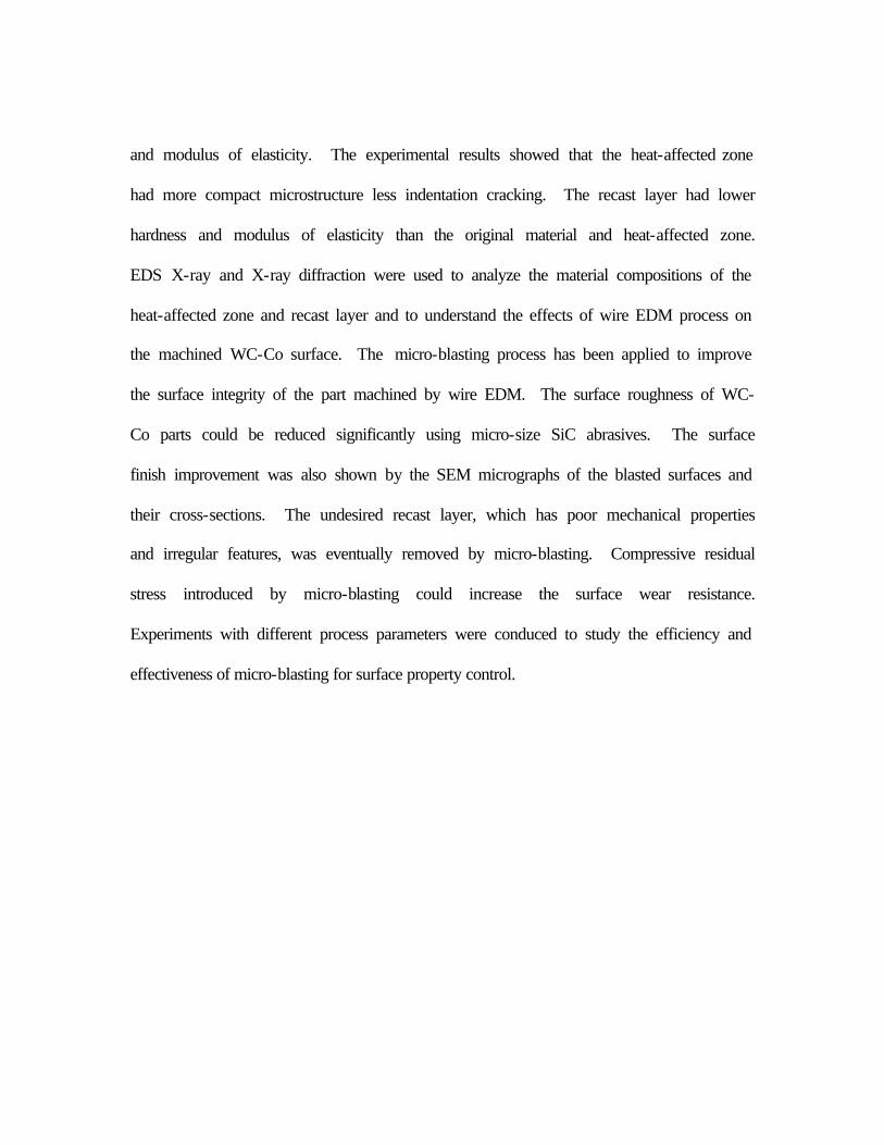
The picture of the underwater spindle used in this study is shown in Fig. 2.3,
respectively. A pair of deep groove silicon nitride ball bearings with stainless steel rings
Chapter 2
13
was used. The gear motor was located above water on the top of the frame. A timing
belt was used to transmit the rotational motion to the R8 collet holder. Precision internal
grinding of the angle in the collect holder was required to achieve the desired runout
specification, which is less than 10 µm on the part 20 mm from the face of the collet.
Fig. 2.3. Side view of the hybrid bearing underwater spindle.
2.3. Spindle Error Analysis
Spindle runout error is an important parameter that can affect the maximum material
removal rate, roundness, and surface finish of cylindrical wire EDM parts. The
Donaldson reversal principle [11] was applied to measure the spindle error. An
electronic indicator with 0.1 µm resolution was used to measure two runout traces on
opposite sides of a 6.35 mm diameter silicon-nitride bar. The spindle error can be
calculated from these two runout traces. A sample spindle error trace at 30 rpm is shown
in Fig. 2.4. The maximum spindle error is defined as the average peak to valley value on
the error trace. Results of the maximum spindle error at 10 different speeds are shown in
Gear Motor
TimingBelt
PulleysCarbon Brush
Holder
Workpiece

Chapter 2
14
Fig. 2.5. Fourier transformation was applied to analyze the spindle runout data to
identify the source of error. Figure 2.6 shows the amplitude of error vs. frequency for
two spindle rotational speeds at 30 and 60 rpm. Four major peaks can be identified.
(i) fo: This is the major peak, which is caused by the off center error. The position of
this peak always corresponds to the spindle rotational speed.
(ii) f1: This is always equal to five times the rotational speed of the spindle, possibly
caused by the form error on bearing races.
(iii)f3 and f4: These two frequencies, 60 and 120 Hz, remain unchanged for different
motor rotational speeds. The frequency peak at 120 Hz is possibly caused by the DC
motor. The amplitude of the frequency at 60 Hz is only significant at certain motor
rotational speeds, such as 90 and 180 rpm. This is possibly caused by resonance at
the spindle’s natural frequency, which is measured as 60 Hz.
-6
-3
0
3
6
0 2 4 6 8Time (s)
Spin
dle
Erro
r (µ
m)
Fig. 2.4. Spindle error at 30 rpm rotational speed.
1/f0
1/f1

Chapter 2
15
5
6
7
8
9
10
0 20 40 60 80 100 120 140 160Spindle Rotation Speed (rpm)
Spin
dle
Erro
r (µ
m)
Fig. 2.5. Spindle error vs. rotational speed.
0
1
2
3
0.1 1 10 100 1000Frequency (Hz)
Ampl
itude
( µm
)
0.1 1 10 100 1000Frequency (Hz)
(a) Spindle rotation speed of 30 rpm. (b) Spindle rotation speed of 60 rpm. Fig. 2.6. FFT Frequency spectrum of the spindle error.
2.4. Material Removal Rate Modeling
The process parameters for modeling the material removal rate in cylindrical wire
EDM of a free-form shape are illustrated in Fig. 2.7. An XY coordinate system is first
f0 = 0.5 Hz (30 rpm)
f1 = 5f0 = 2.5 Hz f3 = 120 Hz
f0 = 1 Hz (60 rpm)
f1 = 5f0 = 5 Hz
f2 = 60 Hz f3 = 120 Hz
0 30 60 90 120 150 180 210 240
Frequency (Hz) 0 0.33 0.67 1.0 1.33 1.67 2.0 2.33 2.67
DC Gearmotor Rotational Speed (rpm)

Chapter 2
16
defined. The X-axis coincides with the rotational axis of the workpiece. The positive
direction of the X-axis is determined by the direction of the wire traverse velocity vector,
vf. The component of the wire traverse velocity vector on the X-axis is always positive.
The Y-axis, in the radial direction of the cylindrical workpiece, is perpendicular to both
the X-axis and the wire. Assume the original workpiece is in cylindrical geometry. R is
the original radius of the workpiece. re is the radius of the effective circle, eC , which
equals the wire radius, rw, plus the width of the gap between the wire and the workpiece.
r is the minimum distance from the effective circle, Ce, to the rotational axis of the
workpiece. vf, the magnitude of vf, is equal to the wire feed rate during machining. α is
the angle from the positive X-axis to vf. The range of α is from –π/2 to π/2.
Fig. 2.7. Parameters in the free form cylindrical wire EDM process.
CL ω R
vf
re
rw
r
αWorkpiece
Wire
Ce
X
Y
Chapter 2
17
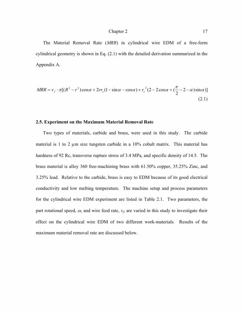
The Material Removal Rate (MRR) in cylindrical wire EDM of a free-form
cylindrical geometry is shown in Eq. (2.1) with the detailed derivation summarized in the
Appendix A.
)]sin)22
(cos22()cossin1(2cos)[( 222 ααπααααπ −−+−+−−+−⋅= eef rrrrRvMRR
(2.1)
2.5. Experiment on the Maximum Material Removal Rate
Two types of materials, carbide and brass, were used in this study. The carbide
material is 1 to 2 µm size tungsten carbide in a 10% cobalt matrix. This material has
hardness of 92 Rc, transverse rupture stress of 3.4 MPa, and specific density of 14.5. The
brass material is alloy 360 free-machining brass with 61.50% copper, 35.25% Zinc, and
3.25% lead. Relative to the carbide, brass is easy to EDM because of its good electrical
conductivity and low melting temperature. The machine setup and process parameters
for the cylindrical wire EDM experiment are listed in Table 2.1. Two parameters, the
part rotational speed, ω, and wire feed rate, vf, are varied in this study to investigate their
effect on the cylindrical wire EDM of two different work-materials. Results of the
maximum material removal rate are discussed below.

Chapter 2
18
Table 2.1. Machine setup for the cylindrical wire EDM experiment. Wire EDM machine Brother HS-5100 Wire manufacturer Charmilles Technologies, BercoCut
Wire material Brass Wire diameter (mm) 0.25 Workpiece material Brass Carbide
Spark cycle (µs) 20 28 On-time (µs) 14 14
(Duty factor, On-time/Spark Cycle) (70%) (50%) Axial direction wire speed (mm/s) 15 18
Wire tension (N) 14.7 14.7 Gap voltage (V) 45 35
The maximum material removal rate (MRRmax) is an important indicator of the
efficiency and cost-effective of the process. Tests are designed to find the MRRmax in
both the cylindrical and 2D wire EDM. Two test configurations to measure the MRRmax
in cylindrical wire EDM are illustrated in Figs. 2.8(a) and 2.8(b). Two 2D wire EDM
tests, as shown in Figs. 2.8(c) and 2.8(d), were also conducted on the same work-material
to evaluate the difference in MRRmax.

Chapter 2
19
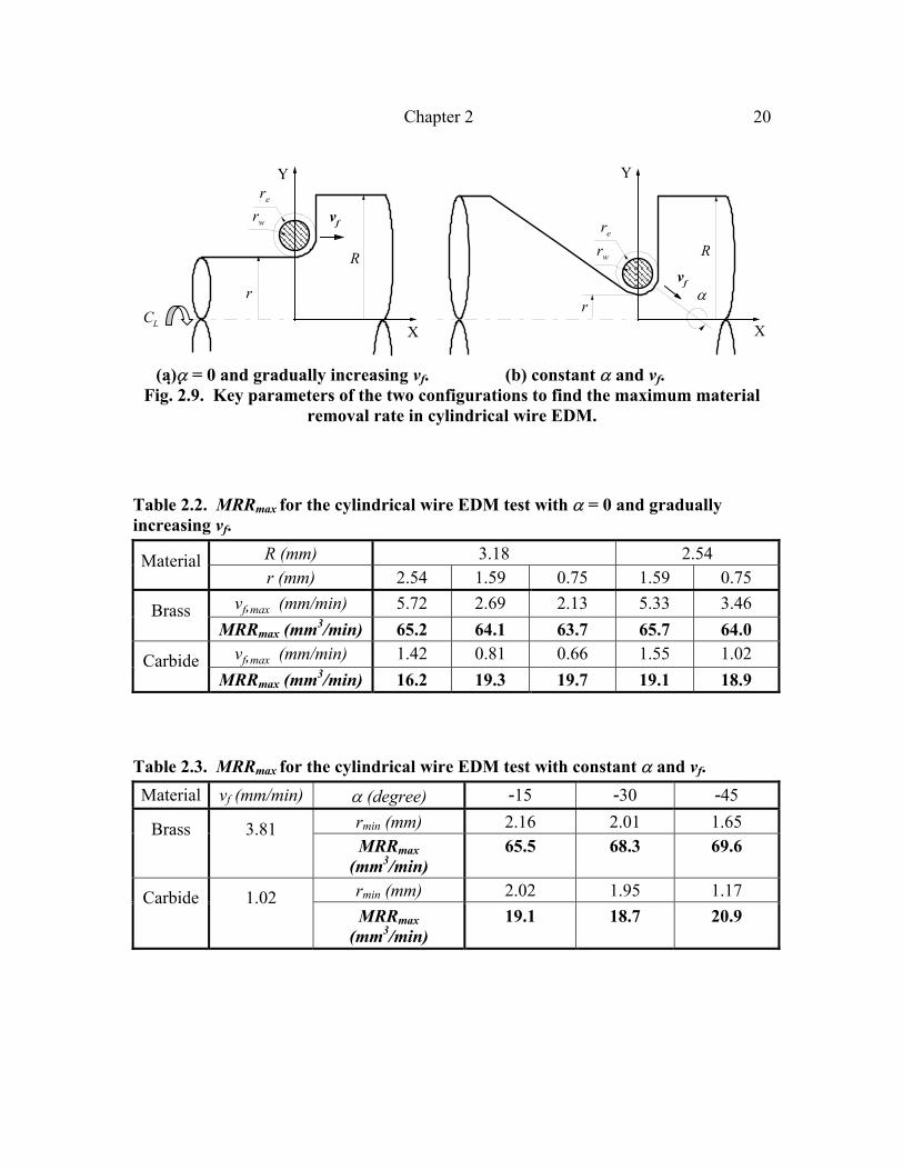
(a) Cylindrical test I. (b) Cylindrical test II. (c) 2D test I. (d) 2D test II. Fig. 2.8. Four test configurations to find the maximum material removal rate.
Key parameters of the two configurations to find the MRRmax in cylindrical wire EDM
are shown in Fig. 2.9. In Fig. 2.9(a), α is set to 0 degree and vf is gradually increased to
the limiting speed, when the short circuit error occurs. This vf is recorded as vf,max and the
MRRmax can be calculated using Eq. (2.1). Another test configuration to measure MRRmax
in cylindrical wire EDM, as shown in Fig. 2.9(b), has constant α and vf. As the wire cuts
into the workpiece, the material removal rate is gradually increased. At the position
when the short circuit error occurs, the material removal rate is recorded as MRRmax.
Two test configurations to find MRRmax for 2D wire EDM at different thickness are
shown in Figs. 2.8(c) and 2.8(d). The vf was gradually increased to find the MRRmax.
Results of MRRmax are summarized in Tables 2.2 to 2.4.
vf vfvf vf
Chapter 2
20
(a)α = 0 and gradually increasing vf. (b) constant α and vf.
Fig. 2.9. Key parameters of the two configurations to find the maximum material removal rate in cylindrical wire EDM.
Table 2.2. MRRmax for the cylindrical wire EDM test with α = 0 and gradually increasing vf.
R (mm) 3.18 2.54 Material r (mm) 2.54 1.59 0.75 1.59 0.75
vf,max (mm/min) 5.72 2.69 2.13 5.33 3.46 Brass MRRmax (mm3/min) 65.2 64.1 63.7 65.7 64.0
vf,max (mm/min) 1.42 0.81 0.66 1.55 1.02 Carbide MRRmax (mm3/min) 16.2 19.3 19.7 19.1 18.9
Table 2.3. MRRmax for the cylindrical wire EDM test with constant α and vf. Material vf (mm/min) α (degree) -15 -30 -45
rmin (mm) 2.16 2.01 1.65 Brass 3.81 MRRmax
(mm3/min) 65.5 68.3 69.6
rmin (mm) 2.02 1.95 1.17 Carbide 1.02 MRRmax
(mm3/min) 19.1 18.7 20.9
αr
re
CL
rw
vf
X
Y
R
r
re
CL
rw vf
X
Y
R

Chapter 2
21
Table 2.4. MRRmax for the 2D wire EDM test. Material Thickness
(mm) re (mm) vf,max (mm/min) MRRmax (mm3/min)
6.35 0.183 23.9 55.5 Brass 3.23 0.183 37.8 44.7 6.35 0.163 4.32 8.94 Carbide 3.23 0.163 8.00 8.42
Several observations can be extracted from the data in Tables 2.2 to 2.4.
1. The brass has much higher material removal rate than the carbide.
2. The MRRmax for cylindrical wire EDM in Tables 2.2 and 2.3 is greater than the 2D
wire EDM results in Table 2.4. The possible cause may be better flushing conditions
in the cylindrical wire EDM. In 2D wire EDM, as shown in Fig. 2.8(c), a narrow gap
exists and affects the flow of high-pressure water jets for flushing. Such situation
does not exist in the cylindrical wire EDM.
3. The MRRmax for 2D wire EDM changes slightly with thickness.
4. For carbide, the MRRmax may not be as high as that in rough grinding. However, this
process does provide the advantage in flexibility to shape the workpiece.
5. The results from the two test configurations for cylindrical wire EDM at different
sizes and angles are close to each other. The maximum material removal rate is
calculated using the material removal rate model under various process setup
parameters. This has verified the concept and mathematical model for the material
removal rate.

Chapter 2
22
Another important observation in this experiment is: the wire breakage is more likely
to occur during cutting at a steeper angle α in the test configuration shown in Fig. 2.9(b).
2.6. Concluding Remarks
The feasibility of applying the cylindrical wire EDM process for high material
removal rate machining of free-form cylindrical geometries was demonstrated in this
study. The mathematical model for the material removal rate of cylindrical wire EDM of
free-form surfaces was derived. Two experimental configurations designed to find the
maximum material removal rates in cylindrical wire EDM were proposed. Results of
each test configurations match each other. The maximum material removal rate for the
cylindrical wire EDM was higher than that in 2D wire EDM of the same work-material.
This indicates that the cylindrical wire EDM is an efficient material removal process.
The spindle was found to be a critical factor in achieving the desired roundness,
surface finish, and material removal rate. The effect of spindle error on part roundness
will be discussed in the following paper. Other refinements to enhance the spindle
accuracy are required to achieve better cylindrical wire EDM results. One of the
advantages of the cylindrical wire EDM process is its ability to machine micro-size
shafts. Preliminary results indicated that a precision spindle is the key factor in the
system for micro-machining applications.

Chapter 2
23
References
[1] Masuzawa, T., Fujino, M., Kobayashi, K., and Suzuki, T., 1985, “Study on Micro-Hole Drilling by EDM,” Bull. Japan Soc. of Prec. Eng., Vol. 20, No. 2, pp. 117-120.
[2] Masuzawa, T., Fujino, M., Kobayashi, K., Suzuki, T., and Fujii, H., 1986, “Wire Electro-Discharge Grinding System for Machining Very Fine Rods,” International Conference on Computer-Aided Production Engineering, Edinburgh, pp. 247-254.
[3] Kuo, C.-L., Masuzawa, T., and Fujino, M., 1992, “High-Precision Micronozzle Fabrication,” IEEE Micro Electro Mechanical Systems ’92, Travemunde Germany, Feb. 4-7, pp.116-121.
[4] Masuzawa, T., Kuo, C.-L., and Fujino, M., 1994, “A Combined Electrical Machining Process for Micronozzle Fabrication,” Annals of CIRP, Vol. 43, pp.189-192.
[5] Langen, H. H., Masuzawa, T., and Fujion, M., 1995, “Modular Method for Microparts Machining and Assembly with Self-Alignment,” Annals of CIRP, pp. 173-176.
[6] Sun, Xi-Qing, Masuzawa, T., and Fujino, M., 1996a, “Micro Ultrasonic machining and its Applications in MEMS,” Sensors and Actuators, Vol. A57, pp. 159-164.
[7] Sun, Xi-Qing, Masuzawa, T., and Fujino, M., 1996b, “Micro Ultrasonic Machining and Self-Aligned Multilayer Machining/Assembly Technologies for 3D Micromachines,” Proceedings of the IEEE Micro Electro Mechanical Systems (MEMS) 1996, Piscataway, NJ, USA, pp. 312-317.
[8] Masuzawa, T. and Tonshoff, H. K., 1997, “Three-Dimensional Micromachining by Machine Tools,” Annals of CIRP, Vol. 46, pp. 621-628.
[9] Yu, Z. Y., Masuzawa, T., and Fujino, M., 1998, “Micro-EDM for Three-Dimensional Cavities - Development of Uniform Wear Method,” Annals of CIRP, Vol. 47, pp. 169-172.
[10] Rajurkar, K. P. and Yu, Z. Y., 2000, “3D Micro-EDM Using CAD/CAM,” Annals of CIRP, Vol. 49, pp. 127-130.
[11] Slocum, A. H., 1992, Precision Machine Design, Prentice Hall.

Chapter 3
24
CHAPTER 3. SURFACE INTEGRITY AND ROUNDNESS OF CYLINDRICAL WIRE ELECTRICAL DISCHARGE MACHINING
3.1. Introduction
The wire Electrical Discharge Machining (EDM) process removes the work-material
by a series of electrical sparks between the workpiece and wire electrode. These sparks
generate craters on the surface and recast layers and heat-affected zones on the sub-
surface of the EDM workpiece. The surface integrity describes the mechanical,
metallurgical, topological, and chemical conditions of the surface region. EDM surfaces
are complicated. A comprehensive description of the surface integrity on EDM surfaces
involves the measurement of surface roughness, depth of heat-affected zone, micro-
hardness, size of surface crater, residual stresses, and endurance limit, etc. [1]. This study
investigates the surface integrity and roundness of cylindrical wire EDM parts and
explores possible ways to adjust process parameters to achieve better surface integrity
and roundness.
Investigations have been carried out to analyze and improve the surface integrity of
parts created by die-sinking EDM [2−5] and wire EDM [6−9]. In representative studies,
the arithmetic average surface roughness, Ra, of the wire EDM processed workpiece was
about 0.2 to 0.4 µm for tool steel [6] and 1.4 to 3.9 µm for metal matrix composites [9].
For the die-sinking EDM process, better surface finish has been reported. The Ra values
could be achieved as low as 0.014 µm on silicon components [5] and 0.6 µm on titanium

Chapter 3
25
carbide parts [4]. Researchers have demonstrated that better surface integrity can be
achieved by optimizing the EDM process parameters [2, 4, 6, 8, 9]. For the cylindrical
wire EDM process, effects of the new process parameters, such as part rotational speed,
on the surface integrity and roundness are not known. A set of preliminary experiments
was conducted to identify key process parameters that significantly affect the material
removal rate and surface roughness. Two sets of experiments, in which these parameters
are varied, were conducted to investigate their effects on material removal rate, surface
integrity, and roundness of cylindrical wire EDM carbide and brass parts.
Scanning Electron Microscopy (SEM) has been a common tool to examine EDM
surfaces [4, 7]. The EDM surface consists of small craters created by electrical sparks
[1]. To improve the EDM surface integrity, the size of craters needs to be small. This
study uses the SEM to examine and estimate the sizes of craters. Sub-surface depths of
the recast layer and heat-affected zone are two other important characteristics of the
EDM surface integrity. The SEM is used to examine the polished cross-section of EDM
surfaces to quantify and compare sub-surface damage for various EDM process
parameters and material removal rates.
In this paper, a mathematical model of the arithmetic surface roughness of an ideal
cylindrical wire EDM surface is introduced in Section 2. Results of surface roughness
and roundness measurements for two sets of experiments intended to produce for high
material removal rate and fine surface roughness, respectively, are presented in Section 3.
SEM micrographs of the surfaces and cross-sections of the sub-surfaces of cylindrical
wire EDM carbide and brass parts are illustrated and discussed in Section 4.

Chapter 3
26
3.2. Surface Finish Modeling
The cross-section of an ideal surface produced by the cylindrical wire EDM process
consists of a series of circular arcs, as shown in Fig. 3.1. The real EDM surface finish is
the combination of this ideal geometry and craters generated by sparks on the surface.
The radius of the circular arc in the ideal surface, re, is equal to the radius of the wire, rw,
plus the gap between wire and workpiece. The same cross-section geometry can be
found on surfaces machined by turning with a radius tool and by ball-end milling
[10−16]. The peak to valley surface roughness, Rt, of the ideal surface with circular arcs
has been studied [12, 13, 15, 16]. However, the closed-form analytical expression of the
commonly used arithmetic average surface roughness, Ra, could not be found in
literature. Only the approximation solution, which replaced the circular arc by a section
of the parabolic curve, is available [15, 16]. The closed-form representation of the
arithmetic average surface roughness, Ra, for an ideal surface consisting of circular arcs is
derived in this study.
Fig. 3.1. Cross-section view of an ideal cylindrical wire EDM surface and the key parameters and coordinate system for mathematical modeling.
Rt
p X
Y222 )( ee rryx =−+
rw
reIdeal surface
Effective circle
Wire
CL ω
Part rotational axis

Chapter 3
27
As shown in Fig. 3.1, after defining an XY coordinate system, one of the circular arcs
on the surface can be expressed as:
222 )( ee rryx =−+ (3.1)
where
22pxp
≤≤− (3.1a)
ω
αcosfvp = (3.1b)
The pitch, p, as shown in Fig. 3.1, is a function of wire feed rate, vf, workpiece
rotation speed, ω, and wire traversing direction, α. The peak-to-valley surface roughness,
Rt, of the ideal surface shown in Fig. 3.1 has been derived [15].
4
22 prrR eet −−= (3.2)
The arithmetic average surface finish, Ra, of the ideal surface is defined by the
following formula:

Chapter 3
28
∫−
−=2/
2/
1 p
pa dxyy
pR (3.3)
where
∫−
=2/
2/
1 p
p
ydxp
y (3.4)
Define S(x) as follows:
∫∫ −−−=−−== )arcsin(21
21)()( 22222
eeeeee r
xrxrxxrdxxrrydxxS (3.5)
Using S(x), y can be expressed as:
)2
(2)]0()2
([22 2/
0
pSp
SpSp
ydxp
yp
=−== ∫ (3.6)
Define another parameter xc as the x coordinate where ( ) yxy c = .
22 yyrx ec −= (3.7)

Chapter 3
29
The analytical expression of arithmetic average roughness, Ra, can be expressed as:
⋅−−⋅−=
−+−= ∫∫ yxpxSpS
pdxyydxyy
pR cc
p
x
x
a
c
c
)22
()(2)2
(2)()(2 2/
0
(3.8)
The extended closed-form solutions and their dimensionless expressions of surface
roughness parameters for a theoretical profile consisting of elliptical or circular arcs will
be presented in Chapter 4.
3.3. Experiments on Surface Finish and Roundness
Cylindrical wire EDM experiments were conducted to investigate the surface finish
and roundness generated under different process parameters and to verify the surface
finish model. The same work-materials, brass and carbide, as in the Chapter 2 are used in
this study.
Two sets of experiments, designated as Experiments I and II, were designed. In
Experiment I, the Material Removal Rate (MRR) was high. The wire feed rate and part
rotational speed were varied to achieve different levels of surface roughness to verify the
proposed surface finish model. In Experiment II, the goal was to adjust EDM process
parameters to achieve the best possible surface finish and roundness. After conducting
preliminary cylindrical wire EDM experiments, two process parameters, the pulse on-
time and wire feed rate, were identified to have significant effects on surface finish.

Chapter 3
30
Also, compared to Experiment I, the material removal rates were reduced significantly in
Experiment II to achieve good surface finish and roundness. Key process parameters for
Experiments I and II are listed in Table 3.1. The other process parameters remain the
same as in the Chapter 2. Table 3.2 summarizes the MRR under different process
parameters in Experiments I and II.
In Experiment I, four part rotation speeds and three wire feed rates were tested for
cylindrical wire EDM of brass and carbide. In total, 24 experiments were conducted.
The test configuration is illustrated in Fig. 3.2 with α = 0, R = 3.175 mm, and r = 2.54
mm. As shown in Table 3.2, the maximum MRR was 13.9 and 52.1 mm3/min for carbide
and brass, respectively. These are about 80% of the maximum MRR observed in [17].
In Experiment II, four pulse on-times and three wire feed rates were tested for brass
and carbide. Similar to Experiment I, 24 tests were conducted. The cutting configuration
shown in Fig. 3.2 with α = 0, R = 2.59 mm, and r = 2.54 mm was used. A thin, 50 µm
layer of work-material was removed. This so called “skim cut” helps improve the surface
finish. A small pitch of p = 0.01 mm was set for all tests in Experiment II to minimize
surface roughness. To maintain the same pitch, the part rotational speeds, as shown in
Table 3.2, were varied for different wire feed rates.

Chapter 3
31
Table 3.1. Machine setup for the Experiments I and II. Experiment I (high MRR) Experiment II (good surface finish)
Work-material Carbide Brass Carbide Brass Spark cycle (µs) 28 20 28 20
Pulse on-time (µs)# 14 14 2~5 2~5 (Duty factor) (50%) (70%) (7~18%) (10~25%)
Wire tension (N) 14.7 14.7 17.64 17.64 Gap voltage (V) 35 45 57 57 Wire feed rate vf
(mm/min)+, # 0.61, 0.91,
1.22 2.54, 3.81,
4.57 0.25, 0.375, 0.5 0.5, 1.0, 1.5
Part rotation speed ω (rpm)+
10, 20, 30, 40
30, 60, 90, 120 25, 37.5, 50 50, 100, 150
+ denotes the set up parameters for Experiment I # denotes the set up parameters for Experiment II
Table 3.2. Material removal rate of Experiments I and II. Work-material Carbide Brass
Pulse on-time (µs) 14 14 Part rotational speed
ω (rpm) 10, 20, 30, 40 30, 60, 90, 180
Wire feed rate vf (mm/min) 1.22 0.91 0.61 4.57 3.81 2.54
Experiment
I (high MRR)
MRR (mm3/min) 13.9 10.4 6.95 52.1 43.4 29.0 Pulse on-time (µs) 2, 3, 4, 5 2, 3, 4, 5
Part rotational speed ω (rpm) 50 37.5 25 150 100 50
Wire feed rate vf (mm/min) 0.5 0.375 0.25 1.5 1.0 0.5
Experiment
II (good
surface finish) MRR (mm3/min) 5.70 4.28 2.85 17.1 11.4 5.70

Chapter 3
32
Fig. 3.2. The configuration of surface finish experiment.
3.3.1. Results of Experiment I
The surface finish and roundness of the 24 parts machined in Experiment I are shown
in Fig. 3.3. The surface finish was measured using a Taylor Hobson Talysurf stylus
profiler. The cutoff was set at 0.8 mm. Five cutoff lengths or 4 mm in total measuring
length was used. The surface roughness parameter Rz (ISO standard), instead of Rt, was
used to represent the peak-to-valley of the measured trace. Rz is defined as the distance
between the average of the top five peaks and the average of the bottom five valleys on
the filtered waviness trace. Since the 4 mm measuring range covers a large number (over
30) of peaks and valleys across an ideal surface shown in Fig. 3.1, Rz is a better indication
than Rt for the true peak-to-valley value on the cylindrical wire EDM surface to avoid the
misleading spikes of peak or valley in the measurement trace.
r
re
C L
rw vf
X
Y
R

Chapter 3
33
Three sets of data are presented in the surface roughness graphs in Fig. 3.3.
• Ideal Surface Roughness: For an ideal surface, the peak-to-valley surface roughness,
Rt, is equal to Rz. Equations (3.2) and (3.8) are used to calculate Rz and Ra,
respectively, of an ideal surface consisting of circular arcs. As shown in Fig. 3.3,
higher part rotational speed and slower wire feed rate generate smaller pitch and
lower Ra and Rz.
• Measured Surface Roughness: Results of the Ra and Rz on the 24 cylindrical wire
EDM carbide and brass parts are shown in Fig. 3.3. The measured values of Ra and
Rz are much higher than the ideal surface roughness due to the additional craters on
the EDM surface. Slightly higher values of measured Ra and Rz were seen on parts
machined at high rotational speeds. This contradicts the trend suggested in the ideal
surface roughness equation. The possible cause is the vibration at higher spindle
speed affects the surface roughness.
• Combined Ideal and 2D Surface Roughness: A set of 2D wire experiments was
conducted on the same work-materials and under the same EDM process parameters
as in Experiment I, except that the workpiece was stationary. Table 3.3 shows the
measured Ra and Rz values of the 2D wire EDM carbide and brass parts under the
same wire feed rate, vf, as used in the cylindrical wire EDM experiments. The three
dashed curves in Fig. 3.3 show results of the addition of the ideal and 2D surface
roughness at three wire feed rates. These three curves have fairly good agreement
with the three measured surface roughness curves. Although simply adding two
surface roughness parameters to get the combined surface roughness lacks scientific

Chapter 3
34
justification, results in Fig. 3.3 suggest a simple method to predict the roughness of
cylindrical wire EDM surface. The SEM micrographs shown in following section
reveal that cylindrical wire EDM surfaces do consist of both the ideal arc-shape in
macro-scale and the surface craters and recast layer in the micro-scale.
Table 3.3. Surface finish of 2D wire EDM parts in Experiment I. Work-material Carbide Brass vf (mm/min) 1.22 0.91 0.61 4.57 3.81 2.54
Ra (µm) 1.80 1.45 1.46 2.89 2.59 2.34 Rz (µm) 11.6 9.23 9.27 18.0 16.7 14.6
The roundness of the machined parts was measured using the Mahr Formtester
MMQ40 form measurement machine. Roundness results, ranging from 8 to 20 µm under
high MRR conditions, are shown in Fig. 3.3. The results indicate that, in general, better
roundness can be achieved at lower wire feed rate vf. This is possibly due to less wire
vibration. The effect of part rotational speed on roundness is not significant.

Chapter 3
35
0
2
4
6
8
Ra
( µm
)
1.22 0.91 0.61
1.22 0.91 0.61
1.22 0.91 0.61
Carbide
4.57 3.81 2.54
4.57 3.81 2.54
4.57 3.81 2.54
Brass
0
10
20
30
40
Rz
( µm
)
Carbide Brass
0
5
10
15
20
25
0 10 20 30 40 50Rotation Speed (rpm)
Roun
dnes
s(µ
m)
Carbide
0 30 60 90 120 150Rotation Speed (rpm)
Brass
Fig. 3.3. The surface finish and roundness of cylindrical wire EDM parts in
Experiment I with high material removal rate.
Measured
Ideal
Combined ideal and 2D
vf (mm/min) vf (mm/min)
Carbide
Carbide Brass
Brass
Brass

Chapter 3
36
3.3.2. Results of Experiment II
The goal of experiment II was to achieve the best possible surface finish and
roundness by adjusting two critical process parameters, the wire feed rate and pulse on-
time. Figure 3.4 shows the surface finish and roundness results for Experiment II. Much
better surface finish and roundness are observed in Experiment II. The shorter pulse on-
time and lower feed rate, in general, created better surface finish and roundness. At the
shortest pulse on-time, 2 µs, significant decreases in the surface roughness and roundness
can be observed. Shorter pulse on-time generates smaller sparks, which, in turn, creates
smaller craters and better surface finish. This can be verified in the SEM micrographs of
EDM surfaces. The best Ra and roundness generated on carbide in this study are 0.68 and
1.7 µm, respectively. These values are comparable to that of rough grinding, which
makes the cylindrical wire EDM process suitable for both high material removal rate and
precision machining of the difficult-to-machine materials. However, this value is not as
low as the 0.014 µm Ra surface roughness reported in EDM of silicon [5]. Better EDM
machines could generate even lower surface roughness.
The 1.7 µm roundness at 2 µs pulse on-time are much smaller than the 6 to 9 µm
spindle error presented in Fig. 2.5 of Chapter 2. The frequency spectrum of the spindle
error presented in Fig. 2.6 of Chapter 2 is used to explain this observation. The fo, the
major peak of the spindle error at the frequency that is equal to the part rotational speed,
is about 2.2 µm in amplitude or 4.4 µm in spindle error. This large off center error does
not affect the roundness because the distance from the rotational axis to the wire remains

Chapter 3
37
constant. The second peak of the spindle error, f1, at the frequency that is equal to five
times the part rotational speed, is about 0.8 µm in amplitude or 1.6 µm in spindle error.
This is identified as the main cause of the 1.7 µm roundness error on cylindrical wire
EDM parts. The third and fourth peaks of the spindle error, f2 and f3, remain at 60 and
120 Hz, respectively, independent of the spindle rotational speed. Since the standard 1-
50 undulation per revolution filter was used in roundness measurement, the spindle error
at these two high frequencies does not show up in the roundness results. In summary,
only the f1 peak of the spindle error spectrum affects the roundness results in low MRR
cylindrical wire EDM conditions.

Chapter 3
38
0
0.5
1
1.5
2
2.5
Ra
( µm
)0.5 0.375 0.25v f (mm/min)
CarbideC bid
1.5 1.0 0.5v f (mm/min)
Brass
3
4
5
6
7
8
9
10
Rz
( µm
)
Carbide
Brass
1
2
3
4
5
6
7
1 2 3 4 5 6Pulse On-Time (µs)
Rou
ndne
ss( µ
m)
Carbide
1 2 3 4 5 6Pulse On-Time (µs)
Brass
Fig. 3.4. The surface finish and roundness of cylindrical wire EDM parts in
Experiment II with improvements on surface finish and roundness.

Chapter 3
39
3.4. SEM Micrographs of EDM Surface and Sub-Surface
SEM is used to examine the surface and sub-surface of cylindrical wire EDM carbide
and brass parts in Experiments I and II. The cylindrical samples were sliced in the radial
direction. Surfaces of sliced cross-sections were polished to observe the sub-surface
damage. The macro-ridges and craters on the surface and the recast layers and heat-
affected zones in the sub-surface of the cylindrical wire EDM parts are presented in the
following three sections.
3.4.1. Macro-ridges
Although regular EDM surfaces are isotropic and have no specific texture or pattern
[1], cylindrical wire EDM surfaces may have macro-ridges, or circular arcs, in the cross-
section. Figure 3.5 shows the surfaces of three cylindrical wire EDM brass parts in
Experiment I with 30 rpm rotational speed and wire feed rates of 4.57, 3.81, and 2.54
mm/min. The corresponding pitches are 152, 127, and 84.7 µm. Similar macro-ridges
exist on carbide parts. Figure 3.5 also shows the ideal surfaces that consist of circular
arcs with the same p and re. These SEM micrographs also verify the surface finish model
described in Section 2.

Chapter 3
40
Ideal arcs
Macro-ridges
p (µm): 152 127 85 Ra (µm): 7.27 4.44 3.19
Fig. 3.5. SEM micrographs of macro-ridges and ideal arcs on surfaces of brass parts in Experiment I (re=0.183 mm).
3.4.2. Craters
The rough surfaces in Experiment I and fine surfaces in Experiment II are observed
using the SEM machine to compare the surface texture and crater size. As illustrated in
the surface finish results in Fig. 3.4, the short, 2 µs, pulse on-time generates fine surface
finish. Under shorter pulse on-time, electrical sparks generate smaller craters on the
surface. For carbide parts, as shown in Fig. 3.6, the rough estimate of the crater size is
about 50, 30, and 20 µm under 14, 5, and 2 µs pulse on-time, respectively. As shown in
Fig. 3.7, slightly bigger craters, estimated as 60, 40, and 25 µm, can be seen on the brass
parts machined under the same pulse on-time. On carbide parts, about 1 to 2 µm size
tungsten carbide grain can be seen on the SEM micrographs in Fig. 3.6.
50 µm50 µm50 µm
50 µm 50 µm50 µm

Chapter 3
41
Experiment I Experiment II Experiment II Ra (µm): 2.53 1.40 0.68 On-time (µs): 14 5 2 ω (rpm): 30 50 25 vf (mm/min): 1.22 0.5 0.25 MRR (mm3/min): 13.9 5.70 2.85
Legend – C: Crater, R: Recast layer, B: Bubble, H: Heat affected zone.
Fig. 3.6. SEM micrographs of surfaces and cross-sections of carbide parts.
10 µm10 µm 10 µm
2 µm 2 µm 2 µm
R
B
H
C C C
H
R
B
R
B
H

Chapter 3
42
Experiment I Experiment II Experiment II Ra (µm): 3.19 1.78 0.98 On-time (µs): 14 5 2 ω (rpm): 30 150 50 vf (mm/min): 2.54 1.5 0.5 MRR (mm3/min): 29.0 17.1 5.70
Legend – C: Crater, R: Recast layer, B: Bubble.
Fig. 3.7. SEM micrographs of surfaces and cross-sections of brass samples.
3.4.3. Sub-surface recast layers and heat-affected zones
The recast layer is defined as the material melted by electrical sparks and resolidified
on the surface without being ejected nor removed by flushing [2]. Below the recast layer
is the heat-affected zone. For the carbide material, the cobalt matrix melts and
resolidifies in the heat-affected zone. The molten cobalt fills the pores in the tungsten
10 µm10 µm 10 µm
10 µm 10 µm 10 µm
C C C
B
R
R
R

Chapter 3
43
carbide. This is observed in the SEM micrographs of the carbide cross-section and is
used to identify the depth of heat-affected zone. Rajurkar and Pandit [18] have studied
the recast layer and heat-affected zones of EDM surfaces and developed a thermal model
to predict the thicknesses of damaged layers. For the die-sinking EDM process, the depth
of the damaged layer was reported to be from 30 to 100 µm for an AISI 4130 steel
workpiece machined with pulse on-time of 100 to 300 µs [4]. Anon [2] has studied the
sub-surface heat-affected zones and recast layers of steel and tungsten carbide using the
die-sinking EDM and have summarized and explained the possible causes for EDM
surface defects.
SEM micrographs of the cross-section of carbide and brass parts machined under both
high and low MRRs (Experiments I and II) are shown in Figs. 3.6 and 3.7. On carbide
parts, the µm size carbide grains can be identified. The recast layer, bubbles in the recast
layer, and heat affected zone of three carbide samples are identified in Fig. 3.6. Under
high MRR at 14 µs pulse on-time, the recast layer, about 3 µm thick, can be clearly
recognized on the surface. Thinner recast layers, less than 2 µm, exist on samples
machined using shorter pulse on-time. Bubbles can be identified in the recast layers of
all three carbide samples. Anon [2] has proposed that these micro-bubbles were
generated by thermal stresses and tension cracking in the recast layer. As shown in Fig.
3.6, the depth of the heat-affected zone is estimated to be about 4, 3, and 2 µm on the
three carbide samples with 14, 5, and 2 µs pulse on-time, respectively.

Chapter 3
44
As shown in Fig. 3.7, very thin recast layers, about 1 µm, can be observed on the
cross-section of three brass samples. No heat-affected zone can be recognized on brass
samples, possibly due to the good thermal conductivity of brass. The heat-affected zone
may exist but cannot be identified in brass samples. For carbide, the contrast of porosity
filled by the molten cobalt makes the identification of the heat-affected zone easier. For
brass material, such phenomenon does not exist. This has made the heat-affect zone
difficult to be identified.
3.5. Concluding Remarks
The surface integrity and roundness of cylindrical wire EDM carbide and brass parts
were investigated. A model with the closed-form solution of the arithmetic average
surface roughness of the ideal surface generated by the cylindrical wire EDM process
was derived and compared to two approximate solutions. Two sets of experiments,
Experiments I and II, were conducted to identify the effects of part rotational speed, wire
feed rate, and pulse on-time on the surface finish and roundness. Experiment I verified
the surface finish model and found that simply adding the roughnesses of 2D wire EDM
surfaces and ideal surfaces provided a good estimate of the surface roughness of
cylindrical wire EDM parts. Experiment II demonstrated that good surface finish and
roundness could be achieved in the cylindrical wire EDM process. The macro-ridges,
surface craters, recast layers, and heat-affected zones were observed, and their sizes were
estimated using the SEM.

Chapter 3
45
In the study, all EDM experiments were conducted on a Brother HS-5100 wire EDM
machine. Experimental results, such as material removal rate, surface roughness, and
roundness, presented in this study may not be directly transferable to other wire EDM
machines using different EDM power supply, wire, and tooling. Concepts presented in
this study, including the quantification of maximum material removal rate, key process
parameters to achieve fine surface finish and roundness, and thickness of recast layers
and heat-affected zones, etc., can be applied for cylindrical wire EDM using other wire
EDM machines on different types of work-materials.
References
[1] Rajurkar, K. P. and Pandit, S. M., 1988, “Recent Progress in Electrical Discharge Machine Technology and Research,” Proceedings of Manufacturing International ’88, Atlanta, GA, USA, Vol. 1, pp. 219-226.
[2] Anon, 1987, “Controlling EDM Surface Integrity,” American Machinist & Automated Manufacturing, Vol. 131, No. 11, pp. 80-83.
[3] Rajurkar, K. P. and Royo, G. F., 1988, “Improvement in EDM performance by R.F. Control and Orbital Motion,” ASME Symposium Volume on Research and Technological Developments in Non-trditional Machining, PED-Vol. 34, pp. 51-62.
[4] Rajurkar, K. P. and Royo, G. F., 1989, “Effect of R.F. Control and Orbital Motion on Surface Integrity of EDM Components,” Journal of Mechanical Working Technology, Vol. 20, pp. 341-352.
[5] Reynaerts, D., Meeusen, W., and Brussel, H. V., 1998, “Machining of Three-Dimensional Microstructures in Silicon by Electro-discharge Machining,” Sensors and Actuators, Vol. A 67, pp. 159-165.
[6] Liao, Y.S. and Woo, J.C., 1997, “The Effects of Machining Settings on the Behavior of Pulse Trains in the WEDM Process,” Journal of Materials Processing Technology, Vol. 71, pp. 433-439.

Chapter 3
46
[7] Williams, R. E. and Rajurkar, K. P., 1991, “Study of Wire Electrical Discharge Machined Surface Characteristics,” Journal of Materials Processing Technology, Vol. 28, pp. 127-138.
[8] Ramulu, M., Jenkins, M. G., and Daigneanult, J. A., 1997, “Spark-Erosion Process Effects on the Properties and Performance of a Tib2 Particulate-Reinforced/Sic Matrix Ceramic Composite,” Ceramic Engineering and Science Proceedings, Vol. 18, No. 3, pp. 227-238.
[9] Gatto, A. and Iuliano, L., 1997, “Cutting Mechanisms and Surface Features of WED Machined Metal Matrix Composites,” Journal of Materials Processing Technology, Vol. 65, pp. 209-214.
[10] Shaw, M. C. and Crowell, J. A., 1965, “Finishing Machining,” Annals of CIRP, Vol. 13, pp. 5-22.
[11] Nassirpour, F. and Wu, S. M., 1977, “Statistical Evaluation of Surface Finish and its Relationship to Cutting Parameters in Turning,” International Journal of Machine Tool Design & Research, Vol. 17, pp.197-208.
[12] Vajpayee, S., 1981, “Analytical Study of Surface Roughness in Turning,” Wear, Vol. 70, pp. 165-175.
[13] Shiraishi, M. and Sato, S., 1990, “Dimensional and Surface Roughness Controls in a Turning Operation,” Transactions of the ASME, Journal of Engineering for Industry, Vol. 112, No. 1, pp. 78-83.
[14] El-wardany, T., Elbestawi, M. A., Attia, M. H., and Mohamed, E., 1992, “Surface Finish in Turning of Hardened Steel,” Engineered surfaces, American Society of Mechanical Engineers, Production Engineering Division, Vol. 62, pp. 141-159.
[15] Whitehouse, D. J., 1994, Handbook of Surface Metrology, Institute of Physics, Bristol, Philadephia.
[16] Cheung, C. F. and Lee, W. B., 2001, “Characterization of Nanosurface Generation in Single-Point Diamond Turning,” International Journal of Machine Tools & Manufacture, Vol. 41, No. 6, pp. 851-875.
[17] Qu, J., Shih, A. J., and Scattergood, R., 2002, “Development of the Cylindrical Wire Electrical Discharge Machining Process, Part I: Concept, Design, and Material Removal Rate,” Journal of Manufacturing Science and Engineering (accepted).
[18] Rajurkar, K. P. and Pandit, S. M., 1984, “Quantitative Expressions for Some Aspects of Surface Integrity of Electro-Discharge Machined Components,” Transactions of ASME Journal of Engineering for Industry, Vol. 106, No. 2, pp. 171-177.

Chapter 4
47
CHAPTER 4. ANALYTICAL SURFACE ROUGHNESS PARAMETERS OF A THEORETICAL PROFILE CONSISTING OF ELLIPTICAL OR CIRCULAR
ARCS
4.1. Introduction
Surface roughness parameters are used to characterize the finish and predict the
functional performance of a surface [1-7]. Many researchers have investigated methods
to measure and quantify the surface roughness and correlated the measurement results to
component performances. De-Chiffre et al. [7] have reviewed the recent developments in
surface metrology. In a recent study of the cylindrical wire EDM surface [8, 9], the
theoretical profile of the machined surface was found to consist of small and repetitive
circular arcs. Similar profiles exist on the surfaces of single-point diamond and
traditional turning with a radius tool tip and on the surfaces machined by ball-end milling
tools [10-22]. The theoretical surface profile with elliptical arcs, a more general case of
circular arcs, can be generated in the flat-end milling process [23, 24]. In this study, three
parameters of the surface consisting of elliptical and circular arcs, the peak-to-valley
roughness Rt, arithmetic average roughness Ra, and root-mean-square roughness Rq, are
investigated. These are three parameters commonly used to evaluate the surface
roughness [2, 3, 5]. Among them, the peak-to-valley roughness Rt for a theoretical
profile consisting of circular arcs has been well studied since the 1960s [6, 10-13, 17, 19,
22]. The approximate estimations of Ra for the theoretical profile formed by circular arcs
have also been reported [23, 24]. However, based on the best of our knowledge, the

Chapter 4
48
closed-form expressions of the Ra and Rq for a theoretical surface profile consisting of
either elliptical or circular arcs have not been reported. One of the goals of this research
is to derive the closed-form analytical expressions of these three roughness parameters,
Rt, Ra, and Rq, for such ideal, theoretical surface profiles.
The real surface generated in machining processes and the profile measured by a
surface finish measurement machine will be different from this theoretical surface profile.
The tool wear, vibration of the tool during machining, elastic deformation and recovery
of the tool and workpiece, build-up edge at tool tip, resolution of the measurement
machine, etc. all create deviation from the theoretical surface profile. Formulas derived
in this study are based purely on geometric consideration. This theoretical model can be
used as prediction of the surface finish and comparison with the measured surface
roughness values to investigate the influence of the work-material, tool behavior, cutting
parameters, and other effects on the machined surface.
Formulas for these three closed-form surface roughness parameters are also arranged
in dimensionless forms. A single dimensionless chart, which includes Rt, Ra, and Rq, can
be used to present results for a wide range of theoretical surface profiles consisting of
elliptical or circular arcs. Different tools, ranging from the sharp single-point diamond
turning with 0.1 mm tool radius, to the conventional turning with 1 mm tool nose radius
and to the ball end-milling with 5 mm tool radius, are used to generate the elliptical or
circular arcs of various sizes.
There are several benefits and applications of such closed-form surface roughness
parameters. First, it can be used for surface roughness prediction and evaluation in

Chapter 4
49
CAD/CAM modeling of machining processes. Compared to the approximate solutions,
the closed-form solution offers more accurate results for a wide range of process
conditions. It is especially beneficial for precision machining processes, such as the
single-point diamond turning and cylindrical wire EDM. Second, the dimensionless
closed-form surface roughness parameters can be represented in a single chart to cover
surface profiles consisting of a wide range of elliptical or circular arc sizes. Third, the
closed-form solution can be used to evaluate different approximate solutions. The error
analysis reveals the limitations and suitable ranges of approximate solutions.
In this paper, the closed-form expressions of the three roughness parameters Rt, Ra,
and Rq for the theoretical surface profile consisting of elliptical arcs are first derived. The
surface roughness parameters in dimensionless form are presented in Sec. 4.3. The
closed-form solutions of Rt, Ra, and Rq for a theoretical profile with circular arcs, a
special case of the elliptical arcs, are discussed in Sec. 4.4. In Sec. 4.5, two approximate
solutions used to estimate the surface roughness parameters, Rt, Ra, and Rq, are derived
and compared with the closed-form solutions.
4.2. Closed-from Expressions of Roughness Parameters for a Theoretical Surface Profile Consisting of Elliptical Arcs
Figure 4.1 illustrates a theoretical surface profile consisting of elliptical arcs. As
shown in Fig. 4.1, a XY coordinate system is first defined. The elliptical arc on the
surface profile can be expressed as

Chapter 4
50
1)(
2
2
2
2
=−
+b
byax
(4.1)
where a and b are the major and minor semi-axis of the elliptical arc, respectively, and
22f
xf
≤≤− (4.2)
The feed, f, as shown in Fig. 4.1, is the distance between two adjacent peaks of the
surface profile. The closed-form expressions of three surface roughness parameters, Rt,
Ra, and Rq, for this surface profile with elliptical arcs are derived in the following three
sections. The derivation of three parameters, a, b, and f, for a measurement profile on the
surface machined by flat-end milling is presented in Appendix B.
Fig. 4.1. A theoretical surface profile consisting of elliptical arcs.
f X
Y Theoretical profile of machined surface 1
)(2
2
2
2
=−
+b
byax
2a
2b Rt
Least squares mean line
y

Chapter 4
51
4.2.1. Peak-to-valley roughness Rt
The peak-to-valley surface roughness, Rt, of the theoretical profile, as defined in Fig.
4.1, is
4
22 f
aab
bRt −−= (4.3)
4.2.2. Arithmetic average roughness Ra
According to ASME B46.1-1995 [25] and ISO 4287-1997 [26], the reference mean
line in surface roughness is either the least squares mean line or filtered mean line. The
least squares mean line is selected. The least squares mean line of this theoretical profile
is a straight line parallel to the X-axis, y = y . Based on the definition of least squares
mean line,
( )0
2/
2/
2
=∂
−∂ ∫−
y
dxyyf
f (4.4)
Thus,
∫−
=2/
2/
1 f
f
ydxf
y (4.5)

Chapter 4
52
In order to simplify the expressions of y , Ra, and Rq, a parameter S(x) is first defined.
∫∫ −−−=−−== )arcsin(22
)()( 2222
axab
xaxa
bbxdxxa
ab
bydxxS (4.6)
Using S(x), y can be expressed as
)2
(2
)]0()2
([22 2/
0
fS
fS
fS
fydx
fy
f
=−== ∫ (4.7)
Define another parameter xc as the x coordinate where ( ) yxy c = on the theoretical
profile.
2
2 yybba
xc −= (4.8)
The arithmetic average surface finish Ra is defined as
∫−
−=2/
2/
1 f
fa dxyy
fR (4.9)

Chapter 4
53
For the theoretical surface profile consisting of elliptical arcs shown in Fig. 4.1, the
closed-form expression of Ra can be derived and simplified with the three pre-defined
parameters, xc, y , and S(x).
[ ])(2
)()(2 2/
0cc
f
x
x
a xSyxf
dxyydxyyf
Rc
c
−⋅=
−+−= ∫∫ (4.10)
where xc, y , and S(xc) are functions of f.
4.2.3. Root-mean-square roughness Rq
The root-mean-square roughness, Rq, is defined as
( )∫−
−=2/
2/
21 f
fq dxyy
fR (4.11)
The closed-form expression of Rq for the theoretical surface profile shown in Fig. 4.1
can be represented by
2
222
2
0
22
122)2(
2abf
ybydxyyyyf
Rf
q −+−=+−= ∫ (4.12)

Chapter 4
54
Instead of using the above implicit form, another method using the parametric form to
derive the closed-form solution of the surface roughness parameters are summarized in
the Appendix C. These two methods give different expressions but same results for the
three surface roughness parameters.
4.3. Roughness Parameters in Dimensionless Form
In this section, the dimensionless form expressions of three surface roughness
parameters are presented. The three dimensionless parameters, Rt /b, Ra /b, and Rq /b, are
expressed as functions of another dimensionless parameter, f/a, which ranges from 0 to 2.
Using the dimensionless form, a single chart can be used to present the surface roughness
results of theoretical surface profiles with a wide range of elliptical arc sizes. The
derivation of dimensionless expressions of the three roughness parameters Rt, Ra, and Rq
are discussed in the following three sections.
4.3.1. Peak-to-valley roughness Rt
Equation (4.3) is rearranged to present the dimensionless peak-to-valley roughness, Rt
/b, as a function of f/a.
2
41
11
−−=
af
bRt (4.13)

Chapter 4
55
Similar dimensionless expression for the theoretical surface profile consisting of
circular arcs has been derived by Shaw and Crowell [12].
4.3.2. Arithmetic average roughness Ra
The S(xc), y , and xc in Eqs. (4.6), (4.7), and (4.8) are first rewritten as functions of the
dimensionless parameter, f/a.
⋅==
af
fbf
Sf
y 1)2
(2
(4.14)
⋅=−=
af
fayybba
xc 2
22 (4.15)
⋅=−−−=
af
fabaxab
xaxa
bbxxS c
cccc 322 )arcsin(
22)( (4.16)
where
−
−−=
af
fa
af
af
f2
arcsin41
121
12
1 (4.17)
−
=
af
faf
faf
f 2112 2 (4.18)
−
−
−
=
af
faf
faf
faf
faf
f 22
2223 arcsin21
121
(4.19)

Chapter 4
56
Substituting Eqs. (4.14) – (4.16) into Eq. (4.10), Ra /b can be expressed in the
dimensionless form.
( )
=
−=
af
fxSyxfbb
Racc
a )(21
(4.20)
where
−
⋅=
af
faf
faf
ffa
af
f a 3212 (4.21)
4.3.3. Root-mean-square roughness Rq
Substituting y in Eq. (4.14) to Eq. (4.12), Rq /b can be expressed as
=−+−=
af
fabf
ybybb
Rq
q2
222
122
1 (4.22)
where
2
12
1 121
2
−
+
−=
af
af
faf
faf
f q (4.23)
Using Eqs. (4.13), (4.20), and (4.22), the three dimensionless surface roughness
parameters, Rt /b, Ra /b, and Rq /b, vs. f/a are illustrated in Fig. 4.2. The chart is zoomed
in at three different levels for small f/a values. To calculate Rt, Ra, and Rq for a
theoretical surface profile consisting of elliptical or circular arcs, f/a is first calculated and

Chapter 4
57
used to find the corresponding Rt /b, Ra /b, and Rq /b in Fig. 4.2. These three
dimensionless values are then multiplied by b to find the value of surface roughness
parameters, Rt, Ra, and Rq. Two examples are used to illustrate this procedure.
Example 1. Flat-end milling with 5 mm radius tool. Assume the major semi-axis a,
minor semi-axis b, and feed f, equal 5, 2, and 2 mm, respectively, then f/a = 0.4. From
Fig. 4.2, the corresponding Rt /b = 0.0202, Ra /b = 0.0052, and Rq /b = 0.0060. By
multiplying b = 2 mm to these three dimensionless parameters, the Rt, Ra, and Rq, of this
theoretical surface profile are 40.4, 10.4, and 12.0 µm, respectively.
Example 2. Single-point diamond turning with 0.1 mm radius tool. In this case, the
theoretical surface profile is formed by circular arcs with rba == = 0.1 mm. Assume
the feed f = 0.008 mm, the f/a = 0.08. From Fig. 4.2, the corresponding Rt /b = 0.00080,
Ra /b = 0.00021, and Rq /b = 0.00024. By multiplying b = 0.1 mm to these three values,
the surface roughness parameters, Rt, Ra, and Rq, of the theoretical surface profile are
0.80, 0.21, and 0.24 µm, respectively.
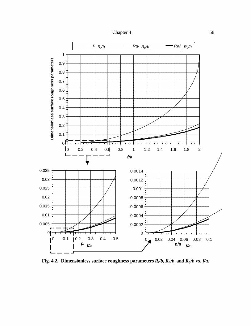
Chapter 4
58
0
0.1
0.2
0.3
0.4
0.5
0.6
0.7
0.8
0.9
1
0 0.2 0.4 0.6 0.8 1 1.2 1.4 1.6 1.8 2
f/a
Dim
ensi
on
less
su
rfac
e ro
ug
hn
ess
par
amet
ers
Rt/b Rq/b Ra/b
0
0.005
0.01
0.015
0.02
0.025
0.03
0.035
0 0.1 0.2 0.3 0.4 0.5p/a
0
0.0002
0.0004
0.0006
0.0008
0.001
0.0012
0.0014
0 0.02 0.04 0.06 0.08 0.1p/a
Fig. 4.2. Dimensionless surface roughness parameters Rt/b, Ra/b, and Rq/b vs. f/a.
Rt/b Rq/b Ra/b
f/a f/a
Chapter 4
59
4.4. Theoretical Surface Profile Consisting of Circular Arcs
Mathematically, the circular arc is a special case of the elliptical arc with rba == .
Theoretical surface profiles consisting of circular arcs can be used to model the surface
generated by turning with radius tools and milling with ball-end mills. The closed-form
expressions of the three surface roughness parameters are derived in the following
sections.
4.4.1. Peak-to-valley roughness Rt
By substituting a and b with r in Eq. (4.3), the closed-form expression of the peak-to-
valley surface roughness, Rt, of a theoretical profile with circular arcs is
4
22 f
rrRt −−= (4.24)
Equation (4.24) has been reported in references [6, 10, 12, 19].
4.4.2. Arithmetic average roughness Ra
The closed-form expression of the arithmetic average roughness Ra in Eq. (4.10) is
still valid for the theoretical profile consisting of circular arcs. Substituting a and b by r
in Eqs. (4.6) and (4.8), S(x) and xc can be expressed as

Chapter 4
60
∫∫ −−−=−−== )arcsin(21
21
)()( 22222
rx
rxrxrxdxxrrydxxS (4.25)
2
2 yyrxc −= (4.26)
The y also has the same expression as in Eq. (4.7).
4.4.3. Root-mean-square roughness Rq
The root-mean-square roughness, Rq, of the theoretical profile consisting of circular
arcs can be derived by substituting a and b with r in Eq. (4.12).
12
22
2 fyryRq −+−= (4.27)
4.5. Approximate Solutions
Two approximate solutions of the three roughness parameters for the theoretical
surface profile consisting of elliptical or circular arcs are presented. Two approximate
solutions, one based on the parabolic approximation and another further simplified
approximation, are derived. Results and comparisons to closed-form solutions are given
in the following sections.

Chapter 4
61
4.5.1. Approximations of the peak-to-valley roughness Rt
Assuming Rt is small and the higher order term Rt2 can be neglected, the peak-to-
valley roughness Rt of the theoretical profile consisting of elliptical arcs can be simplified
to
2
2
8abf
Rt ≅ (4.28)
Substituting a and b by r in Eq. (4.28), the peak-to-valley roughness Rt of a
theoretical surface profile consisting of circular arcs is
r
fRt 8
2
≅ (4.29)
Equation (4.29) has been reported in references [6, 11-13, 17, 19, 22]. Vajpayee [17]
has compared the closed-form, Eq. (4.24), and simplified, Eq. (4.29), expressions of Rt
for surface profile with circular arcs and indicated that the error would be high for a large
f.
4.5.2. Approximations of the arithmetic average roughness Ra
In the past, the parabolic curve was used to approximate the elliptical or circular arcs
to simplify the derivation of Ra. This is defined as the parabolic approximation.
Assuming the surface profile consisting of parabolic curves with the same width (feed)

Chapter 4
62
and height (minor semi-axis) as the elliptical arcs, the approximate Ra can be expressed
as
−−≅
4394 2
2 fa
ab
bRa (4.30)
When the Ra is small, Eq. (4.30) can be further simplified as
2
2
032.0a
bfRa ≅ (4.31)
This is defined as the simplified approximation.
For a theoretical surface profile with circular arcs, the parabolic approximation of Ra
is
−−≅
4394 2
2 frrRa (4.32)
A further simplification of Eq. (4.32) is the simplified approximation.
rf
Ra
2
032.0≅ (4.33)

Chapter 4
63
Equation (4.33) is commonly used to estimate the Ra of a theoretical surface
consisting of circular arcs, as reported in references [6, 22].
4.5.3. Approximations of the root-mean-square roughness Rq
The derivation of Rq can also be simplified by approximating the elliptical arcs by
parabolic curves with the same feed and height. The parabolic approximation of Rq is
−−≅
4532 2
2 fa
ab
bRq (4.34)
The further simplified form of Eq. (4.34) or the simplified approximation of Rq is
2
2
037.0a
bfRq ≅ (4.35)
For a theoretical profile consisting of circular arcs, the parabolic approximation of Rq
is
−−≅
4532 2
2 frrRq (4.36)
Based on Eq. (4.36), the simplified approximation of Rq is

Chapter 4
64
rf
Rq
2
037.0≅ (4.37)
4.5.4. Comparison of the closed-form and approximate solutions
Results of the parabolic and simplified approximations of Rt, Ra, and Rq, comparing to
the closed-form solution, are shown in Fig. 4.3. The parabolic approximations
overestimate and the simplified approximations underestimate the closed-form solution.
More significant errors can be seen at higher f/a. This indicates that both approximate
solutions have good estimations at small f/a. When f/a < 0.5, both approximation
methods gives satisfactory estimations. Replacing a and b by r, Fig. 4.3 can be used for
the theoretical surface with circular arcs. For turning with a radius tool, f/r < 0.5 occurs
when the feed, f, is smaller than the half tool radius, r/2.
Table 4.1 shows more detailed error analysis results for four different values of f/a.
Under the worst case, when f/a = 2, the error is 41.5% and 33.6% for the parabolic
approximation of Ra and Rq and 50.0%, 29.4%, and 33.2% for the simplified
approximation of Rt, Ra and Rq, respectively. Very small error, less than 0.33% for the
parabolic approximation and 1.6% for the simplified approximation, can be seen when f/a
= 0.5. This indicates that the approximation solutions do provide good estimations of the
surface roughness parameters when f/a < 0.5.

Chapter 4
65
0
0.2
0.4
0.6
0.8
1R
t/b
Parabolic Approximation
Closed-form
Simplified Approximation
0
0.05
0.1
0.15
0.2
0.25
0.3
Ra/
b
0
0.05
0.1
0.15
0.2
0.25
0.3
0 0.5 1 1.5 2p/a
Rq/
b
Fig. 4.3. Comparison of closed-form and approximate solutions of surface finish parameters.
f/a

Chapter 4
66
Table 4.1. Error analysis of approximate solutions.
Error (%) Parabolic approximation
(overestimate) Simplified approximation
(underestimate) f/a Ra Rq Rt Ra Rq 0.5 0.33% 0.23% 1.59% 1.50% 1.35% 1 1.53% 1.09% 6.70% 5.50% 5.67%
1.5 4.82% 3.47% 16.93% 13.13% 14.04% 2 41.53% 33.58% 50.00% 29.40% 33.21%
4.6. Concluding Remarks
The closed-form solutions of surface finish parameters, Rt, Ra, and Rq, for the
theoretical profile of a machined surface consisting of elliptical or circular arcs were
derived. It offers accurate surface roughness evaluation for a wide range of process
conditions and can be used in CAD/CAM systems for machining process modeling. Both
the implicit and parametric forms are applied to derive the closed-form solutions. The
dimensionless form of surface roughness parameters, Rt, Ra, and Rq, were also presented.
Two approximation solutions, parabolic approximation and simplified approximation,
were defined and developed to estimate the surface roughness parameters. Limitations of
these approximate solutions were investigated. The comparison of the closed-form and
approximate solutions showed that the parabolic approximation overestimated and the
simplified approximation underestimated the surface roughness parameters. When f/a is
smaller than 0.5, both approximation solutions have good estimation of Rt, Ra, and Rq.

Chapter 4
67
Although a detailed survey was conducted to investigate previous research in this
subject, it is still possible that other researchers could have investigated this basic
problem, perhaps in different format and other approaches. The goal of this study is to
present a compete derivation of the closed-form solution from two different approaches
and to provide a detailed comparison with two approximation solutions.
References
[1] Vajpayee, S., 1973, “Functional Approach to Numerical Assessment of Surface Roughness,” Microtecnic, Vol. 27, pp. 360-361.
[2] Peters, J., Vanherck, and Sastrodinoto, M., 1979, “Assessment of Surface Typology Analysis Techniques,” Annals of CIRP, Vol. 28/2, pp. 539-554.
[3] Thomas, T. R., 1981, “Characterization of Surface Roughness,” Precision Engineering, Vol. 3, pp. 97-104.
[4] Nowicki, B., 1981, “Investigation of the Surface Roughness Range,” Annals of CIRP, Vol. 30, pp. 493-497.
[5] Malburg, M. C., Raja, J., and Whitehouse, D. J., 1993, “Characterization of Surface Texture Generated by Plateau honing Process,” Annals of CIRP, Vol. 42, No. 1, pp. 637-639.
[6] Whitehouse, D. J., 1994, Handbook of Surface Metrology, Institute of Physics, Bristol, Philadephia.
[7] De-Chiffre, L., Lonardo, P., Trumpold, H., Lucca, D. A., Goch, G., Brown, C. A., Raja, J., and Hansen, H. N., 2000, “Quantitative Characterization of Surface Texture,” Annals of CIRP, Vol. 49, No. 2, pp. 635-652.
[8] Qu, J., Shih, A.J., and Scattergood, R., 2001 “Development of the Cylindrical Wire Electrical Discharge Machining Process,” Symposium on Nontraditional Manufacturing Research and Applications, Proceedings of 2001 ASME International Mechanical Engineering Congress and Exposition, Vol. 3, IMECE2001/MED-23343, Nov. 11-16, New York.

Chapter 4
68
[9] Qu, J., Shih, A.J., and Scattergood, R., 2002, “Development of the Cylindrical Wire Electrical Discharge Machining Process, Part II: Surface Integrity and Roundness,” ASME Journal of Manufacturing Science and Engineering (accepted).
[10] Lambert, H. J., 1961-1962, “Two Years of Finish-Turning Research at the Technological University, Delft,” Annals of CIRP, Vol. 10, pp. 246-255.
[11] Sata, T., 1964, “Surface Finish in Metal Cutting,” Annals of CIRP, Vol. 7, pp. 190-197.
[12] Shaw, M. C. and Crowell, J. A., 1965, “Finishing Machining,” Annals of CIRP, Vol. 13, pp. 5-22.
[13] Olsen, K. V., 1968, “Surface Roughness on Turned Steel Components and the Relevant Mathematical Analysis,” The Production Engineer, pp. 593-606.
[14] Wallbank, J., 1979, “Surfaces Generated in Single-Point Diamond Turning,” Wear, Vol. 56, pp. 391-407.
[15] Hasegawa, M., Seireg, A., and Lindberg, R. A., 1976, “Surface Roughness Model for Turning,” Tribology International, Vol. 9, pp. 285-289.
[16] Nassirpour, F. and Wu, S. M., 1977, “Statistical Evaluation of Surface Finish and its Relationship to Cutting Parameters in Turning,” International Journal of Machine Tool Design & Research, Vol. 17, pp. 197-208.
[17] Vajpayee, S., 1981, “Analytical Study of Surface Roughness in Turning,” Wear, Vol. 70, pp. 165-175.
[18] Sata, T., Li, M., Takata, S., Hiroaka, H., Li, C. Q., Xing, X. Z., and Xiao, X. G., 1985 “Analysis of Surface Roughness Generation in Turning Operation and Its Applications,” Annals of CIRP, Vol. 34, pp. 473-476.
[19] Shiraishi, M. and Sato, S., 1990, “Dimensional and Surface Roughness Controls in a Turning Operation,” Transactions of the ASME, Journal of Engineering for Industry, Vol. 112, No. 1, pp. 78-83.
[20] El-wardany, T., Elbestawi, M. A., Attia, M. H., and Mohamed, E., 1992, “Surface Finish in Turning of Hardened Steel,” Engineered surfaces, American Society of Mechanical Engineers, Production Engineering Division, Vol. 62, pp. 141-159.
[21] Salsbury, J. G. and Raja, J., 1995, “Quantitative Metrology for Process Capability Analysis of Turning Centers,” Proceedings of the NAMRC XXIII, Society of Manufacturing Engineers, p. 6.

Chapter 4
69
[22] Cheung, C. F. and Lee, W. B., 2001, “Characterization of Nanosurface Generation in Single-Point Diamond Turning,” International journal of machine tools & manufacture, Vol. 41, No. 6, pp. 851-875.
[23] Lee, Y. S. and Chang, T. C., 1996, “Machined Surface Error Analysis for 5-axis Machining,” International Journal of Production Research, Vol. 34, No. 1, pp. 111-135.
[24] Lee, Y. S., 1998, “Mathematical Modeling of Using Different Endmills and Tool Placement Problems for 4-and 5-axis NC Complex Surface Machining,” International Journal of Production Research, Vol. 36, No.3, pp. 785-814.
[25] ASME B46.1-1995 Surface Texture – Surface Roughness, Waviness, and Lay, 1995.
[26] ISO 4287-1997 Geometrical Product Specifications (GPS) – Surface Texture: Profile Method – Terms, Definitions, and Surface Texture Parameters, 1997.

Chapter 5
70
CHAPTER 5. NANOINDENTATION CHARACTERIZATION OF SURFACE LAYERS OF ELECTRICAL DISCHARGE MACHINED WC-CO
5.1. Introduction
MMC materials are widely used because of their outstanding hardness, wear
resistance, and strength. However, the MMCs are difficult to machine by conventional
processes due to the high hardness and toughness. Alternatively, EDM process has been
used extensively to manufacture the MMC components [1−4]. Although EDM can
machine precise, complex, and intricate MMC components, the surface recast layer and
subsurface heat-affected zone are generated [5]. The surface integrity, including
roughness, size of craters, and depth of recast layer and heat-affected zone, on cylindrical
wire EDM WC-Co surface has been investigated [2]. This study applies nanoindentation,
EDS X-ray, and X-ray diffraction methods to further study the mechanical properties
(hardness and modulus of elasticity) and material compositions of the WC-Co surface
layers machined by the cylindrical wire EDM process.
Indentation has been widely used as an experimental tool to probe the hardness and
modulus of materials by means of load-displacement behavior. Nanoindentation applies
very small load, at the µN level, to the specimen and generates indentation depths in the
sub-µm or nm scale [6]. This makes nanoindentation suitable and effective in measuring
mechanical properties of thin films and small volumes of material and the microstructure
and mechanical properties of MMCs [7−12]. The thickness of EDM recast layer and

Chapter 5
71
heat-affected zone is usually very thin [2−4]. For example, as shown in Fig. 3.6 in
Chapter 3, the thickness of EDM surface layers is less than 3 µm. It is difficult to use
conventional methods to measure and distinguish the mechanical properties of EDM
surface layers. Llanes et al. [3] has used the microscratch tests to characterize the sliding
contact response of the wire EDM WC-Co surfaces. In this study, the nanoindentation
method is applied. In the following section, the experiment setup and sample preparation
are introduced. Experimental results and discussions are then presented in Sec. 5.3.
5.2. Experiment Setup and Sample Preparation
In the past two decades, the nanoindentation method with continuous load-
displacement sensing has been developed and applied by researchers to measure
mechanical properties of thin films and surface layers. The hardness, H, and modulus of
elasticity, E, can be calculated using the following formulas.
A
PH max= (5.1)
A
SEr 2π
= (5.2)
i
i
r EEE)1()1(1 22 υυ −
+−
= (5.3)
Chapter 5
72
where P is the indentation load and Pmax is the peak indentation load, h is the
displacement of the indenter, A is the projected area of the hardness impression, S
(=dP/dh) is the contact stiffness, v is the Poisson’s ratio of the work-material, E is the
modulus of elasticity of the work-material, and Er is the reduced modulus of elasticity
with consideration of the effect of non-rigid indenters. Ei and vi are the modulus of
elasticity and Poisson’s ratio of the indenter, respectively.
In this study, the continuous stiffness measurement method was used to obtain the
contact stiffness, S. Details of this technique and analysis procedure are described in
[6,13,14]. The displacement control was used in the nanoindentation experiment and the
load was dependent on the indenter penetration depth. The hardness and modulus of
elasticity were calculated from the load-displacement curves.
The nanoindentation experiments were conducted at the Oak Ridge National Lab on a
MTS Nano-indenter™ II with the Berkovich diamond indenter, as shown in Fig. 5.1.
The machine was operated to measure the thin surface layers of WC-Co after EDM. A
precision X-Y table with a calibrated distance from the indenter to an optical microscope
was used for accurate positioning of indents.

Chapter 5
73
(a) Front-side view. (b) Close view.
Fig. 5.1. MTS Nano-indenterTM II.
The WC-Co composite used in this study consists of WC particles about 1 µm size
with a volume fraction of 10% cobalt matrix. The SEM micrographs in Fig. 3.6 in
Chapter 3 show the surfaces and cross-sections of three WC-Co parts machined by
cylindrical wire EDM. The sample machined by 5 µs pulse on-time was selected for the
nanoindentation and other material characterization study. Cross-section of the EDM
surface was used for the nanoindentation test.
5.3. Experimental Results and Discussion
In the experiment, multiple indents were performed on the cross-section of the bulk
material, heat-affected zone, and recast layer of the WC-Co part machined by cylindrical
wire EDM. Examples of three sets of nano-indents are shown in Fig. 5.2. The ten nano-
indents in the bulk material are marked by B1 to B10 in Fig. 5.2(a). Four nano-indents in
Indenter
X-Y-Z Stage
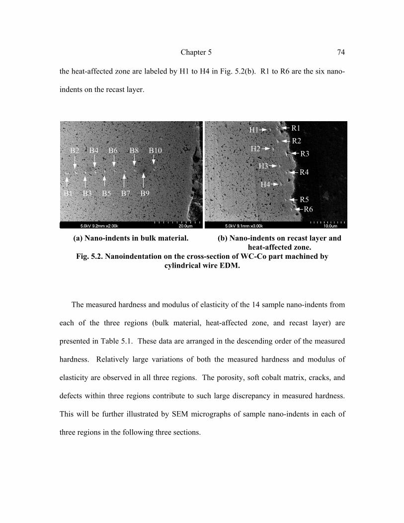
Chapter 5
74
the heat-affected zone are labeled by H1 to H4 in Fig. 5.2(b). R1 to R6 are the six nano-
indents on the recast layer.
(a) Nano-indents in bulk material. (b) Nano-indents on recast layer and heat-affected zone.
Fig. 5.2. Nanoindentation on the cross-section of WC-Co part machined by cylindrical wire EDM.
The measured hardness and modulus of elasticity of the 14 sample nano-indents from
each of the three regions (bulk material, heat-affected zone, and recast layer) are
presented in Table 5.1. These data are arranged in the descending order of the measured
hardness. Relatively large variations of both the measured hardness and modulus of
elasticity are observed in all three regions. The porosity, soft cobalt matrix, cracks, and
defects within three regions contribute to such large discrepancy in measured hardness.
This will be further illustrated by SEM micrographs of sample nano-indents in each of
three regions in the following three sections.
B1 B3 B5 B7 B9
B2 B4 B6 B8 B10
H4
R6
R3
H1
H2
H3
R1 R2
R4
R5

Chapter 5
75
Table 5.1. Hardness and modulus of elasticity of bulk material, heat-affected zone, and recast layer in descending order of the hardness. (Unit: GPa)
Bulk material Heat-affected zone Recast layer Hardness Modulus Hardness Modulus Hardness Modulus
19.7 497 21.0 434 17.3 283 19.3 496 B5 20.4 515 H4 16.6 328 17.4 514 B4 19.9 377 16.4 318 R517.4 479 B10 19.3 438 16.4 312 R616.5 453 18.5 317 15.1 235 16.2 493 B3 18.2 440 15.0 323 13.9 417 B6 18.1 379 H3 14.5 411 R213.8 462 B8 17.9 392 13.4 363 13.2 477 B7 16.5 452 13.2 286 12.3 477 B1 16.4 318 12.7 198 11.6 401 B2 16.1 386 H1 11.2 189 10.8 433 B9 15.2 354 10.9 352 R47.7 238 15.0 394 H2 7.4 294 R17.6 395 15.0 323 5.6 191 R3
Regular nano-indents Irregular nano-indents
5.3.1 Bulk Material
The porosity and soft Co matrix surround the hard WC grain can be identified on the
cross-sectional SEM micrographs of the EDM surface of WC-Co. For the 14 nano-
indents in the bulk material listed in Table 5.1, the measured hardness varied between 7.6
and 19.7 GPa and the modulus of elasticity ranged from 239 to 514 GPa. These indents
were observed using the SEM individually and then separated into two groups: regular
and irregular nano-indents. The irregular nano-indents have pores and/or separation of
grain boundaries on the indent area and show, in general, lower hardness and modulus of
elasticity.

Chapter 5
76
SEM micrographs of two sample nano-indents from each group are shown in Fig. 5.3.
One sample load-displacement curve for one of the nano-indents in each set of frames is
also shown in Fig. 5.3.
• Regular nano-indents. Figure 5.3(a) shows the two regular nano-indents located on
the WC particles. The measured hardness values are 19.7 and 19.3 GPa, respectively.
This level hardness is comparable to the 18 GPa of WC reported in [12]. In contrast
to irregular indents, which hit pores or generated separation of grain boundaries, these
two indented areas had only minor damage on the outside edges.
• Irregular nano-indents. Two sample irregular nano-indents are shown in Fig. 5.3 (b).
A large portion of the indent with 7.7 GPa hardness was on a pore. The indent with
11.6 Gpa hardness had significant separation of grain boundaries around the center,
possibly due to a pore underneath the surface. For these two irregular indents, the
contact area was difficult to define because of the morphology, which resulted in a
decay of measured hardness and modulus.

Chapter 5 77
05
101520
0 100 200 300Displacement (nm)
Loa
d (m
N)
H (GPa) 19.7 GPa 19.3 E (GPa) 496.6 GPa 495.8 Legend: C: Crack, P: Pore
(a) Regular Nano-indents.
05
101520
0 100 200 300Displacement (nm)
Loa
d (m
N)
H (GPa) 7.7 11.6 E (GPa) 238.5 401.6 Legend: S: Separation of grain boundaries, P: Pore
(b) Irregular Nano-indents. Fig. 5.3. Nanoindentation on the bulk material.
5.3.2 Heat-Affected Zone
The heat-affected zone is between the recast layer and bulk material. For the WC-Co
composite, the Co melted and resolidified in the heat-affected zone during the EDM
spark erosion and filled the pores between the WC particles. As shown in Fig. 5.4, this
can be observed in SEM micrographs of the WC-Co cross-section and has been used to
identify the depth of heat-affected zone. The thickness of heat-affected zone in this
sample is about 1−2 µm.
B2
B5 B5
S
P S
S
B2

Chapter 5
78
Unlike nano-indents in the bulk material, separation of grain boundaries rarely
occurred on nano-indents in the heat-affected zone. It is probably due to the Co filled in
pores and gave more consistent support to the WC particles. Variations of measured
hardness and modulus of elasticity in the heat-affected zone are lower than those in the
bulk material and recast layer. The measured hardness varies between 15.0 and 20.4
GPa, and the modulus of elasticity ranges from 323 to 515 GPa.
The nano-indents in the heat-affected zone can also be grouped into regular nano-
indents and irregular nano-indents.
• Regular nano-indents. Figure 5.4 (a) shows two regular nano-indents with hardness
of 20.4 and 18.1 GPa. Similar to the regular nano-indents in bulk material, no pore or
separation of grain boundaries is close to the center of the nano-indent. The
measured results reflect the mechanical properties of WC.
• Irregular nano-indents. Figure 5.4(b) shows two sample irregular nano-indents and a
large overview of a thermal crack extending from the surface, through the recast
layer, to an indent in the heat-affected zone. This study shows that irregular nano-
indents are less likely to occur and smaller variation of indentation results are
observed in the heat-affected zone. It is likely due to the pores filled by the melted
and resolidified Co matrix. The soft Co matrix is one possibility that may affect the
irregular indents in the heat-affected zone. Another possibility is the indent on a
thermal crack initiated from outside the heat-affected zone, as shown in the 15.0 GPa
hardness indent in Fig. 5.4(b).
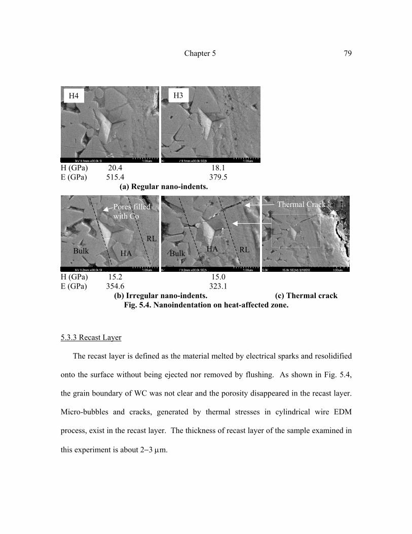
Chapter 5
79
H (GPa) 20.4 18.1 E (GPa) 515.4 379.5 (a) Regular nano-indents.
H (GPa) 15.2 15.0 E (GPa) 354.6 323.1 (b) Irregular nano-indents. (c) Thermal crack
Fig. 5.4. Nanoindentation on heat-affected zone.
5.3.3 Recast Layer
The recast layer is defined as the material melted by electrical sparks and resolidified
onto the surface without being ejected nor removed by flushing. As shown in Fig. 5.4,
the grain boundary of WC was not clear and the porosity disappeared in the recast layer.
Micro-bubbles and cracks, generated by thermal stresses in cylindrical wire EDM
process, exist in the recast layer. The thickness of recast layer of the sample examined in
this experiment is about 2−3 µm.
Thermal Crack Pores filled with Co
HA
RL Bulk
H4 H3
HA RLBulk

Chapter 5
80
EDS X-ray was used to identify the elements in three regions: bulk material, heat-
affected zone, and recast layer. Based on the EDS X-ray analysis, W, Co, and C are the
main elements of the three regions. Only the recast layer has the additional peaks of Cu,
Zn, and O, as shown in Fig. 5.5. The melting and resolidification of brass wire have
deposited the Cu on the recast layer of WC-Co workpiece during EDM spark erosion.
The high temperature also causes the oxidation, which will be investigated in the
following X-ray diffraction analysis. Such contamination of Cu, O, and Zn on the
surface of wire EDM silicon has been reported by Uno, et al. [15] using the X-ray
Photoelectron Spectroscopy (XPS) analysis.
The X-ray diffraction was then used to further analyze the material composition of
the recast layer. A 4-axis (Φ, χ, Ω, 2Θ) goniometer [16] using a copper radiation was
employed for this test. Table 5.2 lists the details of the experimental conditions for the
X-ray diffraction measurements. The X-ray diffraction results are shown in Fig. 5.6.
Major peaks in the scan show that the recast layer contains Tungsten Carbide (WC,
WC1-x, and W2C), Brass (Cu,Zn), and Cobalt Oxide (CoO). Copper Oxide (CuO) and/or
Tungsten Oxide Carbide (W2(C, O)), possibly exist in the recast layer, but are not
distinguished. The results indicate that the tungsten carbide still exist in the recast layer,
even though it cannot be well recognized by the grain boundary as in the bulk material
and heat-affected zone. The Cu and Zn from the brass wire electrode were deposited to
the surface recast layer. Oxides were generated due to the high temperature in EDM
spark erosion.

Chapter 5
81
Fig. 5.5. EDS X-Ray analysis of the recast layer.
0
500
1000
51-0939> Unnamed mineral, syn [NR] - WC
20-1316> WC1-x - Tungsten Carbide
79-0743> W2C - Tungsten Carbide
25-0322> (Cu,Zn) - Brass
43-1004> CoO - Cobalt Oxide
78-0428> CuO - Copper Oxide
22-0959> W2(C,O) - Tungsten Oxide Carbide
30 40 50 60 70 80 90 1002-Theta(°)
Fig. 5.6. X-Ray diffraction analysis of the recast layer.
W
Co
Co Cu W Zn W C O Cu W W

Chapter 5
82
Table 5.2. Experimental conditions of the X-ray diffraction measurements. Parameter Condition
Equipment
Scintag PTS goniometer MAC Science 18 kW rotating anode generator
Scintag liquid N2-cooled Ge detector Power 8 kW; 40 kV, 200 mA
Radiation Cu, λ = 1.54059 Å, Line Mode Incident Optic OSMIC “X-ray mirror” (CMF12.5 – INFCu8)
Incidence slit width 0.5 mm Receiving slit acceptance 0.25°; radial divergence limiting (RDL) Soller slit
Source to specimen distance 360 mm Specimen to back slit distance 280 mm
Scans Θ−2Θ; 0.02° 2Θ/step; 0.2°/min
The measured hardness and modulus of elasticity of the recast layer are generally
lower than those of the bulk material and heat-affected zone. The deposition of brass
from the wire electrode, oxidation of material, and thermal cracks are the causes for the
deterioration of mechanical properties in the recast layer. Regular and irregular nano-
indents in the recast layer are identified.
• Regular nano-indents. Figure 5.7(a) shows two regular nano-indents in the area
without clear grain boundary of WC, pores, and cracks. The measured hardness and
modulus of elasticity were lower than those regular indents in the bulk material and
heat-affected zone.
• Irregular nano-indents. The measured hardness and modulus of elasticity were highly
affected by thermal cracks, bubbles, and edges in the recast layer. Some indents with
very low hardness and modulus of elasticity were observed.

Chapter 5
83
H (GPa) 16.4 16.4 E (GPa) 318.2 312.6
(a) Regular nano-indents.
H (GPa) 12.7 7.4 E (GPa) 198.3 294.6 (b) Irregular nano-indents.
Fig. 5.7. Nanoindentation on the recast layer.
5.4. Concluding Remarks
Mechanical properties of the bulk material, sub-surface heat-affected zone, and
surface recast layer of a WC-Co part machined by cylindrical wire EDM were
investigated using the nanoindentation. SEM micrographs were used to classify indents
in these three regions to the regular and irregular indents. Irregular indents were caused
by the porosity, soft Co matrix, thermal cracks, and separation of grain boundaries
R6
R1
HA RL

Chapter 5
84
generated during indentation. The hardness and modulus of elasticity of the regular
indents in bulk material and heat-affected zone are comparable to those of WC.
The heat-affected zone had more compact microstructure and better support of the
WC particles. Less indentation cracking was observed in the heat-affected zone. For the
regular indents, the recast layer had lower hardness and modulus of elasticity compared
to the bulk material and heat-affected zone. The grain boundary of WC was not clear in
the recast layer. EDS X-ray and X-ray diffraction analysis showed the WC still existed in
the recast layer. In addition, the deposition of Cu and Zn from brass wire electrode and
oxidation of Co and Cu on the recast layer could be identified. These effects and thermal
cracks and bubbles all contribute to the deterioration of mechanical properties of the
recast layer.
References
[1] Qu, J., Shih, A. J., and Scattergood, R., 2002, “Development of the Cylindrical Wire Electrical Discharge Machining Process, Part I: Concept, Design, and Material Removal Rate,” Journal of Manufacturing Science and Engineering (accepted).
[2] Qu, J., Shih, A. J., and Scattergood, R., 2002, “Development of the Cylindrical Wire Electrical Discharge Machining Process, Part II: Surface Integrity and Roundness,” Journal of Manufacturing Science and Engineering (accepted).
[3] Llanes, L., Idanez, E., Martinez, E., Casas, B., Esteve, J., 2001, “ Influence of Electrical Discharge Machining on the Sliding Contact Response of Cemented Carbides,” International Journal of Refractory Metals and Hard Materials, Vol. 19, No. 1, pp. 35-40.
[4] Ramulu, M., Jenkins, M. G., and Daigneanult, J. A., 1997, “Spark-Erosion Process Effects on the Properties and Performance of a Tib2 Particulate-Reinforced/Sic Matrix Ceramic Composite,” Ceramic Engineering and Science Proceedings, Vol. 18, No. 3, pp. 227-238.

Chapter 5
85
[5] Williams, R. E. and Rajurkar, K. P., 1991, “Study of Wire Electrical Discharge Machined Surface Characteristics,” Journal of Materials Processing Technology, Vol. 28, pp. 127-138.
[6] Oliver, W.C. and Pharr, G.M., 1992, “An Improved Technique for Determining Hardness and Modulus of elasticity Using Load and Displacement Sensing Indentation Experiments,” Journal of Materials Research, Vol. 7, No. 6, pp. 1564-1580.
[7] Riester, L. and Ferber, M.K., 1994, “Investigation of Depth-Area Relationships Associated with Nanoindentations,” Proceedings of International Engineering Foundation Conference on the Plastic Deformation of Ceramics, August 7-12, 1994, Snowbird, Utah, pp. 185-194
[8] Tsui, T.Y. and Pharr, G.M., 1999, “Substrate Effects on Nanoindentation Mechanical Property Measurement of Soft Films on Hard Substrates,” Journal of Materials Research, Vol. 11, No. 1, pp. 292-301.
[9] Zhang, J.S., Liu, X.J., Cui, H., Duan, X.J., Sun, Z.Q., and Chen, G.L., 1997, “Microstructure and Properties of Spray-Deposited 2014+15 Vol Pct Sic Particulate-Reinforced Metal Matrix Composite,” Metallurgical and Materials Transactions A: Physical Metallurgy and Materials Science, Vol. 28A, No. 5, pp. 1261-1269.
[10] Gee, M.G., Roebuck, B., Lindahl, P., and Andren, H.O., 1996, ”Constituent Phase Nanoindentation of WC/Co and Ti(C, N) Hard Metals,” Materials Science and Engineering A: Structural Materials: Properties, Microstructure and Processing, Vol. 209, No. 1-2, pp. 128-136.
[11] Zhou, Y., Asaki, R., Soe, W.H., Yamamoto, R., Chen, R., and Iwabuchi, A., 1999, ”Hardness Anomaly, Plastic Deformation Work and Fretting Wear Properties of Polycrystalline TiN/CrM Multilayers,” Wear, Vol. 236, No. 1, pp. 159-164.
[12] Zambrano, G., Prieto, P., Perez, F., Rincon, C., Galinda, H., Cota, A.L., Esteve, J., and Martinez, E., 1998, “Hardness and Morphological Characterization of WC Thin Films,” Surface and Coatings Technology, Vol. 108, No. 1-3, pp. 323-327.
[13] Pethica, J.B. and Oliver, W.C., 1989, “Mechanical properties of Nanometer Volumes of Material: Use of the Elastic Response of Small Area Indentations,” Thin Films Stresses and Mechanical Properties Materials Research Society Symposium Proceedings, Vol. 130, pp. 13-23.
[14] Oliver, W.C. and Pethica, J.B., 1989, “Method for Continuous Determination of the Elastic Stiffness of Contact Between Two Bodies,” U.S. Patent No. 4848141.

Chapter 5
86
[15] Uno, Y., Okada, A., Okamoto, Y., and Hirano, T., 2000, “Wire EDM Slicing of Monocrystalline Silicon Ingot,” Proceedings of 2000 ASPE Annual Meeting, Vol. 22, pp. 172-175.
[16] Krause, H. and Haase, A., 1986, “X-Ray Diffraction System PTS for Powder, Texture and Stress Analysis,” Experimental Techniques of Texture Analysis, DGM Informationsgesellschaft•Verlag, H. J. Bunge, Editor. pp. 405-408.

Chapter 6
87
CHAPTER 6. ABRASIVE MICRO-BLASTING OF WIRE ELECTRICAL DISCHARGE MACHINED WC-CO COMPOSITE
6.1. Introduction
EDM process has been used extensively to manufacture the MMC components [1−4].
Although EDM can machine precise, complex, and intricate MMC components, the
surface recast layer and subsurface heat-affected zone deteriorate the surface mechanical
properties [5,6]. Figure 6.1 shows SEM micrographs of the surfaces and cross-sections
of a WC-Co sample machined by rough cut and skim cut under 14 and 2 µs pulse on-
time, respectively. Electrical sparks generate craters, bubbles, and cracks on the recast
layer, marked by RL. A sub-surface heat-affected zone, denoted by HA, with essentially
no porosity can be identified between the recast layer and bulk material. Pulse on-time is
an important EDM process parameter that affects the thickness of the recast layer and
heat-affected zone [2]. Keeping the spark cycle at 28 µs, the longer (14 µs) pulse on-time
generates thicker recast layer and heat-affected zone, as shown in Fig. 6.1(a). The
material removal rate is, in general, higher for the longer pulse on-time.
The surface integrity, including roughness, size of craters, and depth of recast layer
and heat-affected zone, on cylindrical wire EDM WC-Co surface has been investigated in
Chapter 3 [2]. Nanoindentation, EDS X-ray, and X-ray diffraction methods were applied
to study the mechanical properties (hardness and modulus of elasticity) and material
compositions of the WC-Co surface layers machined by the cylindrical wire EDM
process in Chapter 5 [6]. The heat-affected zone of the EDM WC-Co part has more

Chapter 6
88
compact microstructure than the bulk material and shows high hardness and modulus of
elasticity [6]. However, the recast layer with craters and thermal cracks and bubbles
deteriorates the surface finish and mechanical properties of the wire EDM WC-Co
surface [2,6], and should be removed for surface sensitive applications. The diamond
wheel grinding process has been used for this task, but it is limited to certain size, and to
a flat or convex circular surface. The erosion properties of WC-Co composite has been
studied by [7,8]. In this study, micro-blasting is proposed, as a finishing process, to
improve the surface integrity of the WC-Co parts machined by wire EDM. The material
removal mechanism of blasting is erosion wear.
(Legend – CR: Crater, RL: Recast layer, and HA: Heat affected zone)
(a) Rough cut (14 µs pulse on-time). (b) Skim cut (2 µs pulse on-time).
Fig. 6.1. SEM micrographs of the surface and cross-section of a WC-Co part machined by wire EDM.
CR
HA
RL
HA
RL
CR

Chapter 6
89
Abrasive blasting has been widely applied to surface treatment, increasing roughness
for higher adhesion strength in coating process [9,10], or reducing roughness for better
surface integrity and higher strength and wear resistance with compressive residual stress
introduced by the blasting process [11−14]. Micro-blasting using very small size media
is particularly suitable for microfabrication and surface treatment of micro components
[9,15]. The micro size abrasives along with low air pressure enable the micro-blasting to
do microfabrication or treat the surface of micro parts. The EDM process, without macro
cutting force, is suitable to machine micro components [16,17]. Improving the surface
integrity of the EDM micro parts has been an important research topic. The thickness of
EDM recast layer and heat-affected zone is usually very thin [2−4]. For example, as
shown in Fig. 6.1, the thickness of EDM surface layers is less than 3 µm.
In this study, micro-blasting was applied to the micro cylindrical wire EDM WC-Co
parts. Figure 6.2 shows a 100 µm diameter WC-Co cylinder machined by cylindrical
wire EDM and then blasted using 6~12 µm size black SiC abrasive at 0.138 MPa air
pressure for 5 s. The close-views illustrate that the craters on the surface generated by
EDM sparks were eliminated by blasting and the surface turned to be smoother.

Chapter 6
90
(a) Over view of the (b) Close view of the (c) Close view of the micro part before blasting. surface before blasting. surface after blasting.
Fig. 6.2. Micro-blasting on a micro cylindrical wire EDM WC-Co part.
Lee and Deng [13,18,19] have used abrasive blasting to treat the wire EDM ceramic
composite surface to improve the surface integrity, strength, and reliability. There was
lack of optimization of the blasting process and correlation between the process
parameters. In this study, blasting with micro size SiC abrasives is applied to the wire
EDM WC-Co surface at multiple process settings to investigate the erosion wear and
surface integrity improvement. Effects of key process parameters of micro-blasting,
abrasive size, air pressure, and blasting time, on the both rough and fine wire EDM WC-
Co surfaces are explored. The micro-blasting process is also applied to the micro round
shape parts machined by cylindrical wire EDM. Scanning Electron Microscopy (SEM) is
used to examine the surface and polished cross-section of the blasted wire EDM WC-Co
samples.

Chapter 6
91
The sample preparation and experiment setup are introduced in the following section.
The experimental results and discussions are presented in Sec. 6.3.
6.2. Sample Preparation and Experiment Setup
The WC-Co composite consisting of WC particles about 1 µm size in 10% cobalt
matrix was used as the work-material in this study. It has 92 Rc hardness, 3.4 MPa
transverse rupture stress, and 14.5 specific density. Two sets of WC-Co parts were
prepared for micro-blasting, which were machined by wire EDM using rough cut and
skim cut technologies, and represented by R and S in the following sections, respectively.
The process parameters of the two wire EDM cutting technologies are given in Table 6.1.
Table 6.1. Process parameters of wire EDM rough cut and skim cut. Cutting technology Rough cut Skim cut
Spark cycle (µs) 28 28 On-time (µs) 14 2
Axial wire speed (mm/s) 18 15 Wire tension (N) 14.7 17.6 Gap voltage (V) 45 60
Micro-blasting experiments on wire EDM WC-Co surfaces were conducted to
investigate the erosion wear rate and surface integrity improvement. All experiments
were conducted on a Mangum blasting machine, manufactured by Blast-it-all. Two types
of black SiC abrasives were used in the micro-blasting experiments. The abrasive A, as

Chapter 6
92
shown in Fig. 6.3(a), is the mix of 4~8, 6~12, and 8~16 µm sizes SiC particles, and the
size of abrasive B is in the range of 6~12 µm, as shown in Fig. 6.3(b).
(a) Abrasive I. (b) Abrasive II.
Fig. 6.3. Two sizes of SiC abrasives.
The process parameters of the experiments are listed in Table 6.2. In this study, zero
incident angle was used, which means the abrasive velocity vector is normal to the
surface. Two key parameters of the blasting process, the air pressure and blasting time
were varied in this study to explore their effect on the erosion wear and surface integrity.
The WC-Co workpieces for erosion wear rate experiment were machined using wire
EDM rough cut. In the surface integrity experiment, the micro-blasting was applied to
the surfaces of both rough cut and skim cut WC-Co parts.
Table 6.2. Process parameters of Micro-blasting experiments. Experiment Erosion wear rate Surface integrity
Air pressure (MPa) 0.138, 0.276 0.138, 0.276 Blasting time (s) 10, 20, 30 5, 10, 15

Chapter 6
93
6.3. Experimental Results and Discussions
The results of the erosion wear and surface integrity improvement experiments are
summarized below.
6.3.1. Erosion wear Rate
The micro-blasting erosion wear rate was measured by the weight reduction during
the blasting process. In the erosion wear rate experiment, the wire EDM rough cut WC-
Co part was blasted using abrasives A and B at 0.276 and 0.138 MPa air pressure by 10,
20, and 30 s blasting durations. Figure 6.4 shows the experimental results of erosion
wear for abrasive A and B at two air pressures and three blasting durations. Some
observations could be made:
• Effect of abrasive size. The erosion wear rate using abrasive A was higher than
that of abrasive B under the same blasting condition, because abrasive A had the
relatively larger size particles.
• Effect of air pressure. The higher air pressure (0.276 MPa) generated higher
erosion wear than the lower air pressure (0.138 MPa). Almost doubled erosion
wear rate was achieved for doubled air pressure.
• Effect of blasting duration. More material was removed at the first 10 s than the
following blasting durations. That is probably because of the weak recast layer
was removed at beginning. The recast layer had lower hardness and modulus of
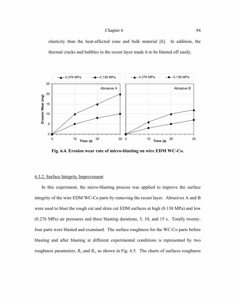
Chapter 6
94
elasticity than the heat-affected zone and bulk material [6]. In addition, the
thermal cracks and bubbles in the recast layer made it to be blasted off easily.
MicroBlasting - SiC 600 mesh
0
5
10
15
20
25
0 10 20 30Time (s)
Eros
ion
Wea
r (m
g)
0.276 MPa 0.138 MPa MicroBlasting - SiC 600 mesh
0 10 20 30Time (s)
0.276 MPa 0.138 MPa
Fig. 6.4. Erosion wear rate of micro-blasting on wire EDM WC-Co.
6.3.2. Surface Integrity Improvement
In this experiment, the micro-blasting process was applied to improve the surface
integrity of the wire EDM WC-Co parts by removing the recast layer. Abrasives A and B
were used to blast the rough cut and skim cut EDM surfaces at high (0.138 MPa) and low
(0.276 MPa) air pressures and three blasting durations, 5, 10, and 15 s. Totally twenty-
four parts were blasted and examined. The surface roughness for the WC-Co parts before
blasting and after blasting at different experimental conditions is represented by two
roughness parameters, Ra and Rz, as shown in Fig. 6.5. The charts of surfaces roughness
Abrasive A Abrasive B

Chapter 6
95
indicate that the surface finish improvement of micro-blasting highly depends on the
original surface integrity and blasting parameters.
SEM was used to examine the surfaces and sub-surfaces of the WC-Co parts to
investigate the effect of the micro-blasting. The SEM micrographs of the surfaces and
polished cross-sections of selected blasted parts are shown in Figs. 6.6~6.10.
Based on the surface roughness results and SEM micrographs, the original EDM
surface, abrasive size, air pressure, blasting duration all together determined the surface
integrity after blasting.

Chapter 6
96
• Effect of original EDM surface. The rough cut WC-Co parts had 2~3 µm thick
recast layer and 1.3~1.4 µm Ra and 8~9 µm Rz surface roughness. The surface
and cross-section of a sample parts are shown in Fig. 6.1(a). The recast layer was
removed after 15 s blasting, as shown in Figs. 6.6, 6.7, and 6.8, and the surface
roughness could be reduced significantly, down to about 0.8 µm Ra and 4 µm Rz,
as shown in Fig. 6.5. As the surface and cross-section shown in Fig. 6.1(b), the
skim cut EDM parts had thinner recast layer (about 1 µm). The surface roughness
was about 0.7~0.9 µm Ra and 5~7 µm Rz for the skim cut parts. Figures 6.9 and
6.10 show that the recast layer had been removed after 5 s blasting. Using
abrasive A at low air pressure and abrasive B at both high and low air pressure,
the roughness values did not drop down much, as shown in Fig. 6.5, though the
surfaces look smoother in the SEM micrographs (Fig. 6.9). The surface finish
may turn to be worse using abrasive A at high air pressure, as illustrated in Figs.
6.5 and 6.10.
• Effect of abrasive size and air pressure. The abrasive A with larger size particles
and/or high air pressure (0.276 MPa) removed the recast layer faster and reduced
the surface roughness of rough cut parts more efficiently than the lower air
pressure (0.138 MPa), as shown in roughness charts (Fig. 6.5) and SEM
micrographs (Figs. 6.6~6.9). However, the skim cut surface may be deteriorated
by short time blasting using abrasive A and high air pressure, as shown in Figs.
6.5 and 6.10.

Chapter 6
97
• Effect of blasting duration. Basically, the longer blasting time, the better surface
finish. For certain abrasive and air pressure, the surface roughness will reach the
bottom line after long enough blasting duration, no matter the original surface
finish. Figure 6.5 shows the trend, though some roughness values did not drop
down to the limit because of insufficient blasting time.
Some interesting pattern can be seen on the blasted surfaces, as shown in Figs.
6.6~6.10. The topography was probably generated by the EDM process, but messed with
the rough recast layer, and revealed by the blasting process.

Chapter 6
98
0
0.5
1
1.5
2
R a (
µm)
0.276 MPa 0.138 MPa0.276 MPa 0.138 MPa
0
5
5
2
0.276 MPa 0.138 MPa0.276 MPa 0.138 MPa
0
3
6
9
12
0 5 10 15Time (s)
R z (
m)
0
3
6
9
2
0 5 10 15Time (s) Fig. 6.5. Surface finish improvement on wire EDM WC-Co using micro-blasting.
(a) 5 s blasting time. (b) 10 s blasting time. (c) 15 s blasting time.
Fig. 6.6. SEM micrographs of surfaces and cross-sections of the wire EDM rough cut WC-CO part after micro-blasting using abrasive A at 0.276 MPa air pressure.
Abrasive A Abrasive B
Abrasive B Abrasive A
Rough cut Skim cut
Rough cutSkim cut

Chapter 6
99
(a) 5 s blasting time. (b) 10 s blasting time. (c) 15 s blasting time.
Fig. 6.7. SEM micrographs of surfaces and cross-sections of the wire EDM rough cut WC-CO part after micro-blasting using abrasive A at 0.138 MPa air pressure.
(a) 5 s blasting time. (b) 10 s blasting time. (c) 15 s blasting time.
Fig. 6.8. SEM micrographs of surfaces and cross-sections of the wire EDM rough cut WC-CO part after micro-blasting using abrasive B at 0.138 MPa air pressure.

Chapter 6
100
(a) 5 s blasting time. (b) 10 s blasting time. (c) 15 s blasting time.
Fig. 6.9. SEM micrographs of surfaces and cross-sections of the wire EDM skim cut WC-CO part after micro-blasting using abrasive B at 0.276 MPa air pressure.
(a) 5 s blasting time. (b) 10 s blasting time. (c) 15 s blasting time.
Fig. 6.10. SEM micrographs of surfaces and cross-sections of the wire EDM skim cut WC-CO part after micro-blasting using abrasive A at 0.276 MPa air pressure.

Chapter 6
101
6.4. Concluding Remarks
The abrasive micro-blasting process was used to improve the surface integrity of the
WC-Co parts machined by wire EDM. Two sizes of black SiC abrasives, two air
pressures, and three blasting durations were applied to both wire EDM rough cut and
skim cut WC-Co surfaces to explore the effects of blasting parameters on the surface
integrity. The SEM micrographs showed that the recast layer was eventually removed by
micro-blasting. The larger size abrasive and higher air pressure had higher erosion wear
rate and reduce the surface roughness more effectively. The surface roughness of EDM
rough cut parts was reduced significantly, Ra dropping down from 1.34 to about 0.7 µm,
while little improvement was made on the surface finish of skim cut parts.
References
[1] Qu, J., Shih, A. J., and Scattergood, R., 2002, “Development of the Cylindrical Wire Electrical Discharge Machining Process, Part I: Concept, Design, and Material Removal Rate,” Journal of Manufacturing Science and Engineering (accepted).
[2] Qu, J., Shih, A. J., and Scattergood, R., 2002, “Development of the Cylindrical Wire Electrical Discharge Machining Process, Part II: Surface Integrity and Roundness,” Journal of Manufacturing Science and Engineering (accepted).
[3] Llanes, L., Idanez, E., Martinez, E., Casas, B., Esteve, J., 2001, “ Influence of Electrical Discharge Machining on the Sliding Contact Response of Cemented Carbides,” International Journal of Refractory Metals and Hard Materials, Vol. 19, No. 1, pp. 35-40.
[4] Ramulu, M., Jenkins, M. G., and Daigneanult, J. A., 1997, “Spark-Erosion Process Effects on the Properties and Performance of a Tib2 Particulate-Reinforced/Sic Matrix Ceramic Composite,” Ceramic Engineering and Science Proceedings, Vol. 18, No. 3, pp. 227-238.

Chapter 6
102
[5] Williams, R. E. and Rajurkar, K. P., 1991, “Study of Wire Electrical Discharge Machined Surface Characteristics,” Journal of Mechanical Processing Technology, Vol. 28, pp. 127-138.
[6] Qu, J., Riester, L., Shih, A. J., Scattergood, R., Lara-Curzio, E., and Watkins, T., 2002, “Nanoindentation Characterization of Surface Layers of Electrical Discharge Machined Wc-Co,” Materials Science and Engineering-A (to be submitted).
[7] Beste, U., Hammerstrom, L., Engqvist, H., Rimlinger, S., and Jacobson, S., 2001, “Particle erosion of cemented carbides with low Co content,” Wear, Vol. 250-251, pp. 809-817.
[8] Pugsley, V.A., Allen, C., 1999, “Microstructure/property relationships in the cavitation erosion of tungsten carbide-cobalt,” Wear, Vol. 233-235, pp. 93-103.
[9] Bouzakis, K.D., Michailidis, N., Hadjiyiannis, S., Efstathiou, K., Pavlidou, E., Erkens, G., Rambadt, S., and Wirth, I., 2001, “Improvement of PVD Coated Inserts Cutting Performance Through Appropriate Mechanical Treatments of Substrate and Coating Surface,” Surface and Coating Technology, Vol. 146-147, pp. 443-450.
[10] Guilemany, J.M., Llorca, I.N., and Szabo, P.J., 1996, “Residual Stress Characterization of Grit Blasted Steel Surfaces,” Surface Engineering, Vol. 12, No. 1, pp. 77-79.
[11] Hung, N.P., Teong, L.H., and Yoong, C.M., 1996, “ Review of Unconventional Machining of Metal Matrix Composites,” Proceedings of the 1996 3rd Biennial Joint Conference on Engineering Systems Design and Analysis, ASME PD, New York, NY, Vol. 75, No. 3, pp. 47-53.
[12] Ben Rhouma, A., Braham, C., Fitzpatrick, M.E., Ledion, J., and Sidhom, H., “Effects of Surface Preparation on Pitting Resistance, Residual Stress, and Stress Corrosion Cracking in Austenitic Stainless Steels,” Journal of Materials Engineering and Performance, Vol. 10, No. 5, pp. 507-514.
[13] Deng, J. and Le, T.C., 2000, “Techniques for Improved Surface Integrity of Electrodischarge Machined Ceramic Composites,” Surface Engineering, Vol. 16, No. 5, pp. 411-414,
[14] Lai, M.O. and Siew, Y.H., 1995, “Fatigue Properties of Cold Worked Holes,” Journal of Materials Processing Technology, Vol. 48, pp. 533-540.
[15] Schlautmann, S., Wensink, H., Schasfoort, R., Elwenspoek, M., and Berg, A., 2001, “Powder-Blasting Technology as an Alternative Tool for Microfabrication of Capillary Electrophoresis Chips with Integrated Conductivity Sensors,” Journal of Micromechanics and Microengineering, Vol. 11, pp. 386-389.

Chapter 6
103
[16] Masuzawa, T. and Tonshoff, H. K., 1997, “Three-Dimensional Micromachining by Machine Tools,” Annals of CIRP, Vol. 46, pp. 621-628.
[17] Rajurkar, K. P. and Yu, Z. Y., 2000, “3D Micro-EDM Using CAD/CAM,” Annals of CIRP, Vol. 49, pp. 127-130.
[18] Lee, T.C. and Zhang, J.H., 1997, “Surface Treatment of Wire Electro-Discharge Machined Engineering Ceramics by Abrasive Blasting,” Journal of Adhesion Science Technology, Vol. 12, No. 6, pp. 585-592.
[19] Lee, T. and Deng, J., 2002, “ Mechanical Surface Treatments of Electro-Discharge Machined (EDMed) Ceramic Composite for Improved Strength and Reliability,” Journal of European Ceramic Society, Vol. 22, pp. 545-550.

Chapter 7 103
CHAPTER 7. CONCLUSIONS
The cylindrical wire EDM process was developed for machining free-form cylindrical
components of difficult-to-machine materials, such as the Metal Matrix Composites.
This process is suitable to machine micro-size shafts, because of the minimum cutting
force. A precise, flexible, and corrosion-resistant underwater rotary spindle was designed
and the spindle errors were analyzed using FFT. The spindle was found to be a critical
factor in achieving the desired roundness, surface finish, and material removal rate.
The mathematical models of the material removal rate and surface finish for any free-
form cylindrical geometry were derived and verified by experiments. The closed-form
surface finish model was extended to a general solution for any theoretical surface profile
consisting of elliptical or circular arcs. It offers accurate surface roughness evaluation for
a wide range of process conditions and can be used in CAD/CAM systems for machining
process modeling.
Experimental results indicated that higher maximum material removal rate might be
achieved in the cylindrical wire EDM than the conventional 2D wire EDM. This
indicates that the cylindrical wire EDM is an efficient material removal process. Two
sets of experiments were conducted to identify the effects of part rotational speed, wire
feed rate, and pulse on-time on the surface roughness and roundness. It was
demonstrated that good surface finish and low roundness error could be achieved in the
cylindrical wire EDM process.

Chapter 7 104
The surface integrity and material composition of cylindrical wire EDM WC-Co
surface layers were investigated using SEM, Nanoindentation, EDS X-ray, and X-ray
diffraction. Cylindrical EDM WC-Co surfaces were first examined using SEM to
identify the EDM surface features, e.g. craters, and thermal cracks and bubbles. The
recast layer and heat-affected zone were then observed and quantified on the SEM
micrographs of the cross-sections of the EDM parts. The effects of process parameters
on the surface roughness and the thickness of damage layers were also studied. The
nanoindentation was applied to a cylindrical wire EDM WC-Co part to investigate the
mechanical properties of the bulk material, heat-affected zone, and recast layer. SEM
was used to observe and classify the indents to the regular and irregular indents. Irregular
indents were caused by the porosity, soft Co matrix, thermal cracks, and cracking
generated during indentation. The hardness and modulus of elasticity of the regular
indents in bulk material and heat-affected zone are comparable to those of WC. The
heat-affected zone had more compact microstructure less indentation cracking. For the
regular indents, the recast layer had lower hardness and modulus of elasticity compared
to the bulk material and heat-affected zone. EDS X-ray and X-ray diffraction analysis
showed the WC still existed in the recast layer, though the grain boundary of WC was not
clear. In addition, the deposition of Cu and Zn from brass wire electrode and oxidation of
Co and Cu on the recast layer could be identified. These effects and thermal cracks and
bubbles all contribute to the deterioration of mechanical properties of the recast layer.
The micro-blasting process with micro-size SiC abrasives was applied to improve the
surface integrity of the EDM surfaces. The recast layer with poor mechanical properties

Chapter 7 105
was eventually removed and the surface roughness of WC-Co parts was reduced.
Compressive residual stress introduced by micro-blasting could result in higher surface
wear resistance. The effects of micro-blasting process parameters on the surface integrity
of EDM WC-Co surfaces were investigated to increase the process efficiency. SEM was
also used to examine the blasted surfaces and their cross-sections.

106
APPENDICES

Appendices
107
Appendix A. Material Removal Rate Modeling in Cylindrical Wire EDM
The mathematical model of Material Removal Rate (MRR) in cylindrical wire EDM
of a free-form shape is presented. This is a geometrical model, which does not include
the process parameters, such as voltage and current. Figure A.1 shows the free-form
cylindrical geometry machined by the cylindrical wire EDM process. The effective
circles of the wire at time t–∆t and t are represented by tteC ∆− and t
eC , respectively. ∆r is
the change of r during ∆t, and can be expressed as:
αsin⋅∆=∆ tvr f (A.1)
R
r-∆rr
α
re
CL
vf ∆t
VIVIII
VII
rw
vf
Wire attime t-∆t
Wire attime t
Cet
Cet-∆t
X
Y
+
-
Fig. A.1. Free form geometry in cylindrical wire EDM.
ω

Appendices
108
The volume of the material removed from t–∆t to t is denoted as V. As shown in Fig.
A.1, V is the volume swept by the hatched area around the X-axis. V can be divided into
three portions, VI, VII, and VIII.
IIIIII VVVV ++= (A.2)
VI is a ring with outer radius R, inner radius err + , and thickness re.
eeI rrrRV ])([ 22 +−= π (A.3)
An enlarged figure of the volume VII is shown in Fig. A.2.
r
re
CL
r+re
Y
X
Va
θ
α
Vc
Cet
L1
L2
L3
L4
Vb
α
+
-
vf
β = α
Fig. A.2. Calculation of VII.
ω

Appendices
109
cbaII VVVV ++= (A.4)
where
−+= eeea rrrrV
32)(
22 ππ (A.4a)
++−= ααααπ 22 cossin
32cossin)( eeeb rrrrV (A.4b)
++−+= ααααπ 32 sin
32)cossin)(( eeec rrrrV (A.4c)
Substituting Eqs. (A.4a) – (A.4c) into Eq. (A.4),
)]sin1(32)
2)(([ 32 ααππ −−−+= eeeII rrrrV (A.5)
VIII is the combination of cylinders, cones and rotated pies, as shown in Fig. A.3.
JKGHKGEDMCDABCMCDEFNBFHIII VVVVVVV −−−−+= (A.6)

Appendices
110
where
απ tan2 rRVNBFH ∆= (A.6a)
( ) eeABCM rrrrRV ⋅+∆−−= ][ 22π (A.6b)
ααπ tan])cos()[(31 33
eeePEDPFCCDEF rrrrrrrVVV −+∆−−+∆−−=−= (A.6c)
( ) ( )[ ] αααπ tan/coscos31 33
eeeeTKGTDEKDEG rrrrrrrVVV −+−−+∆−−=−= (A.6d)
ααπ tan])cos()[(31 33
eeeSGKSHJJKGH rrrrrVVV −+−+−=−= (A.6e)
( ) ( )
−−
−+∆−= ααππ sin1
32
232
eeeMCD rrrrrV (A.6f)
R
r-∆rr
vf
re
CL
vf ∆t
AB
CD
E F G H TSP
J
N
M
K
VIII
X
Y
α
+
-
Fig. A.3. Calculation of VIII.
ω

Appendices
111
Substituting the formula of VI, VII, and VIII into Eq. (A.2), V can be expressed as:
( )r
r
rrrR
rrrrV
e
e
e
∆⋅
+−−−+
−−+−
+
∆⋅
+−++∆⋅
−=
22
tan2
sin2
1tan
1sin
12tan
1
)(1sin
1tan
1tan
1)(tan31
2
22
23
πααα
αααπ
αααπ
απ
(A.7)
Substituting Eq. (A.1) into Eq. (A.7),
)]sin)22
(cos22(
)cossin1(2
cos)[(
2
22
0
ααπα
αα
απ
−−+−+
−−+
−⋅=∆
=→∆
e
e
ft
r
rr
rRvt
VLimMRR
(A.8)

Appendices
112
Appendix B. Derivation of Semi-Axes a and b and Feed f for a Measurement Profile on the Surface Machined by Flat-End Milling
Figure B.1 shows a grooved surface machined by a flat-end mill with radius r and
pitch p between parallel tool paths. The trace for surface finish measurement is at an
angle θ relative to the velocity vector of the end mill, V. The definitions of the X- and Y-
axes are the same as on the surface measurement profile presented in Fig. 1. X-axis is
tangent to the valley of the elliptical arcs and Y-axis is perpendicular to the nominal
surface. On the XY plane, the theoretical profile consists of elliptical arcs with semi-axes
a and b and feed f. Two angles, α and β, are used to define the orientation of the tool
relative to the XYZ coordinate. A coordinate X’Y’Z’ with origin at O’ on the axis of the
tool is illustrated in Fig. A.1. X’, Y’, and Z’ axes are parallel to X, Y, and Z axes,
respectively. Line O’D is the projection of the tool axis O’C on the X’-Z’ plane. α is the
angle between X’-axis and O’D and β is the angle between O’C and O’D.
The semi-axes a and b and feed f of the elliptical arc on the measuring profile are:
( )θ
θαsin
cos −= ra (B.1)
βcosrb = (B.2)
θsin
pf = (B.3)

Appendices
113
Fig. B.1. The measurement profile on the surface machined by flat-end milling.
X
Y
X’ Z’
β α
θ
VSurface roughness measurement profile
1)(2
2
2
2
=−
+b
byax
r
f
2a
2bV
Y’
O’
D
p
C
End mill
Z
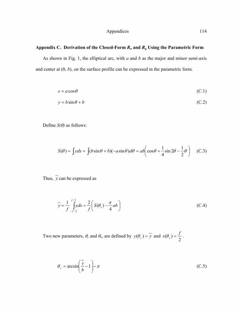
Appendices
114
Appendix C. Derivation of the Closed-Form Ra and Rq Using the Parametric Form
As shown in Fig. 1, the elliptical arc, with a and b as the major and minor semi-axis
and center at (0, b), on the surface profile can be expressed in the parametric form.
θcosax = (C.1)
bby += θsin (C.2)
Define S(θ) as follows:
−+=−+== ∫∫ θθθθθθθ
212sin
41cos)sin)(sin()( abdabbydxS (C.3)
Thus, y can be expressed as
−== ∫
−
abSf
ydxf
y e
f
f 4)(21 2/
2/
πθ (C.4)
Two new parameters, θc and θe, are defined by yy c =)(θ and 2
)( fx e =θ .
πθ −
−= 1arcsin
by
c (C.5)

Appendices
115
−=
af
e 2arccosθ (C.6)
The arithmetic average roughness Ra and root-mean-square roughness Rq of the
theoretical profile then can be derived and represented by the following formulas.
[ ]abfbaSfSaf
dxyyf
R ccec
f
fa πθπθθθ +−⋅−⋅=−= ∫
−
cos2)(2)(cos811 22
2/
2/
(C.7)
( ) 2
2222/
2/
2
1221
abfybydxyy
fR
f
fq −+−=−= ∫
−
(C.8)