ABSTRACT OF THESIS FUNCTIONAL ENHANCEMENT AND APPLICATIONS ...
372
ABSTRACT OF THESIS FUNCTIONAL ENHANCEMENT AND APPLICATIONS DEVELOPMENT FOR A HYBRID, HETEROGENEOUS SINGLE-CHIP MULTIPROCESSOR ARCHITECTURE Reconfigurable and dynamic computer architecture is an exciting area of research that is rapidly expanding to meet the requirements of compute intense real and non-real time applications in key areas such as cryptography, signal/radar processing and other areas. To meet the demands of such applications, a parallel single-chip heterogeneous Hybrid Data/Command Architecture (HDCA) has been proposed. This single-chip multi- processor architecture system is reconfigurable at three levels: application, node and processor level. It is currently being developed and experimentally verified via a three phase prototyping process. A first phase prototype with very limited functionality has been developed. This initial prototype was used as a base to make further enhancements to improve functionality and performance resulting in a second phase virtual prototype, which is the subject of this thesis. In the work reported here, major contributions are in further enhancing the functionality of the system by adding additional processors, by making the system reconfigurable at the node level, by enhancing the ability of the system to fork to more than two processes and by designing some more complex real/non-real time applications which make use of and can be used to test and evaluate enhanced and new functionality added to the architecture. A working proof of concept of the architecture is achieved by Hardware Description Language (HDL) based development and use of a Virtual Prototype of the architecture. The Virtual Prototype was used to evaluate the architecture functionality and performance in executing several newly developed example applications. Recommendations are made to further improve the system functionality. KEYWORDS: Reconfigurable Computing, System on a Chip, Embedded Systems, Multi-Processor System Sridhar Hegde 12/15/2004
Transcript of ABSTRACT OF THESIS FUNCTIONAL ENHANCEMENT AND APPLICATIONS ...

ABSTRACT OF THESIS
FUNCTIONAL ENHANCEMENT AND APPLICATIONS DEVELOPMENT FOR A HYBRID, HETEROGENEOUS SINGLE-CHIP MULTIPROCESSOR
ARCHITECTURE
Reconfigurable and dynamic computer architecture is an exciting area of research that is rapidly expanding to meet the requirements of compute intense real and non-real time applications in key areas such as cryptography, signal/radar processing and other areas. To meet the demands of such applications, a parallel single-chip heterogeneous Hybrid Data/Command Architecture (HDCA) has been proposed. This single-chip multi-processor architecture system is reconfigurable at three levels: application, node and processor level. It is currently being developed and experimentally verified via a three phase prototyping process. A first phase prototype with very limited functionality has been developed. This initial prototype was used as a base to make further enhancements to improve functionality and performance resulting in a second phase virtual prototype, which is the subject of this thesis. In the work reported here, major contributions are in further enhancing the functionality of the system by adding additional processors, by making the system reconfigurable at the node level, by enhancing the ability of the system to fork to more than two processes and by designing some more complex real/non-real time applications which make use of and can be used to test and evaluate enhanced and new functionality added to the architecture. A working proof of concept of the architecture is achieved by Hardware Description Language (HDL) based development and use of a Virtual Prototype of the architecture. The Virtual Prototype was used to evaluate the architecture functionality and performance in executing several newly developed example applications. Recommendations are made to further improve the system functionality. KEYWORDS: Reconfigurable Computing, System on a Chip, Embedded Systems, Multi-Processor System Sridhar Hegde 12/15/2004

FUNCTIONAL ENHANCEMENT AND APPLICATIONS DEVELOPMENT FOR A
HYBRID HETEROGENEOUS SINGLE-CHIP MULTIPROCESSOR
ARCHITECTURE
By
Sridhar Hegde
Dr. J. Robert Heath (Director of Thesis)
Dr. YuMing Zhang
(Director of Graduate Studies)
12/15/2004

RULES FOR THE USE OF THESES
Unpublished theses submitted for the Master’s degree and deposited in the University of Kentucky Library are as a rule open for inspection, but are to be used only with due regard to the rights of the authors. Bibliographical references may be noted, but quotations or summaries of parts may be published only with the permission of the author, and with the usual scholarly acknowledgments. Extensive copying or publication of the theses in whole or in part also requires the consent of the Dean of the Graduate School of the University of Kentucky. A library that borrows this thesis for use by its patrons is expected to secure the signature or each user. Name Date

THESIS
Sridhar Hegde
The Graduate School
University of Kentucky
2004

DESIGN ENHANCEMENT AND APPLICATIONS DEVELOPMENT FOR A
HYBRID, HETEROGENEOUS, SINGLE-CHIP MULTIPROCESSOR
ARCHITECTURE
___________________________________
THESIS __________________________________________
A thesis submitted in partial fulfillment of the requirements for the degree of Master of
Science in Electrical Engineering in the College of Engineering at the University of Kentucky
By
Sridhar Hegde
Lexington, Kentucky
Director: Dr. J. Robert Heath, Associate Professor of Electrical and Computer
Engineering
Lexington, Kentucky
2004

MASTER’S THESIS RELEASE
I authorize the University of Kentucky Libraries to reproduce this thesis in whole or in part for purposes of research
Signed: _________________________________
Date: 12/15/2004

iii
ACKNOWLEDGEMENTS The following thesis, while an individual work, benefited from the insights and direction
of several people. First, my Thesis Chair, Dr. J Robert Heath, exemplifies the high
quality scholarship to which I aspire. Next, I wish to thank the complete Thesis
Committee: Dr. J Robert Heath, Dr. Hank Dietz, and Dr. Bill Dieter. Each individual
provided insights that guided and challenged my thinking, substantially improving the
finished product. In addition to the technical and instrumental assistance above, I
received equally important assistance from family and friends. Finally, I wish to thank
the respondents of my study (who remain anonymous for confidentiality purposes). Their
comments and insights created an informative and interesting project with opportunities
for future work.

iv
TABLE OF CONTENTS
Acknowledgements .......................................................................................................... iii List of Tables .................................................................................................................... vi List of Figures.................................................................................................................. vii Chapter One : Introduction
1.1 Background............................................................................................................... 1 1.2 HDCA Concepts ....................................................................................................... 4 1.3 Goals and Objectives of the Thesis........................................................................... 6 1.4 Thesis Summary........................................................................................................ 7
Chapter Two : Background and System Details 2.1 HDCA and Related Background Work..................................................................... 9 2.2 PRT Mapper............................................................................................................ 12 2.3 Multi-Function Queue............................................................................................. 15 2.3.1 FIFO Block .......................................................................................................... 16 2.3.2 Rate Block............................................................................................................ 17 2.4 The Computing Elements ....................................................................................... 18 2.5 The CE Controller................................................................................................... 21 2.6 Interface Controller................................................................................................. 23 2.7 The Multiplier and the Divider CEs........................................................................ 28
Chapter Three : Design Methodology and Modifications 3.1 Design Methodology............................................................................................... 32
3.1.1 Problem Definition........................................................................................... 32 3.1.2 Requirements definition................................................................................... 33
3.2 Design Flow Approach ........................................................................................... 33 3.3 Modifications to the First Phase Prototype............................................................. 38
3.3.1 PE Controller ................................................................................................... 38 3.3.2 Interface Controller.......................................................................................... 39 3.3.3 Crossbar Interconnect Network ....................................................................... 41 3.3.4 Input Rom for the Data .................................................................................... 42 3.3.5 Multiplier CE ................................................................................................... 43 3.3.6 Dynamic Load Balancing Circuit .................................................................... 43 3.3.7 Memory-Register Computer Architecture CEs ............................................... 44
3.4 Second Version (Phase) HDCA System................................................................. 46 Chapter Four : Virtual Prototype Development
4.1 The Virtual Prototype ............................................................................................. 49 4.3 FPGA Based Chip Resource Utilization Reports ................................................... 50
4.3.1 Device Utilization report for the Multiple Forking Application...................... 50 4.3.2 The Delay and Timing Summary Report – Application One .......................... 51 4.3.3 Device Utilization Report for Un-pipelined Integer Manipulation Algorithm 51 4.3.4 Delay and Timing Summary Report – Application Two................................. 52
4.4 Timing Constraints Definition for Post Implementation Simulation...................... 53 Chapter Five : Functional Enhancements to the HDCA
5.1 Dynamic Node Level Reconfigurability................................................................. 54 5.1.1 Introduction and Concept..................................................................................... 54

v
5.1.2 Assignment Policy and Implementation .......................................................... 55 5.2 Multiple Forking ..................................................................................................... 65
5.2.1 Introduction and Concept................................................................................. 65 5.2.2 Implementation ................................................................................................ 66 5.2.3 Post Place n Route Simulation Validation of an Application with Multiple Forking...................................................................................................................... 67
Chapter Six : Example Applications Development, Testing and Evaluation for Enhanced Fully Functional HDCA
6.1 Application One: Acyclic Integer Averaging Algorithm........................................ 77 6.2 Acyclic Application Two – 2x 2 Matrix Multiplication Algorithm ....................... 87 6.3 Acyclic Application 3 – 3x3 by 3x2 matrix multiplication algorithm with performance evaluation and gate count comparisons ................................................. 104 6.4 Application Four – Acyclic Pipelined integer manipulation algorithm................ 129 6.5 Complex Non-Deterministic Cyclic Value Swap Application ............................. 158
Chapter Seven : Conclusions and Recommendations 7.0 Conclusion ............................................................................................................ 185 7.1 Recommendations................................................................................................. 186
Appendix A.................................................................................................................... 188 Appendix B .................................................................................................................... 332 References...................................................................................................................... 354 Vita ................................................................................................................................. 358
vi
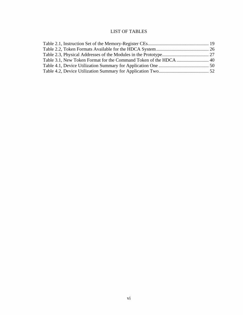
LIST OF TABLES Table 2.1, Instruction Set of the Memory-Register CEs................................................... 19 Table 2.2, Token Formats Available for the HDCA System............................................ 26 Table 2.3, Physical Addresses of the Modules in the Prototype....................................... 27 Table 3.1, New Token Format for the Command Token of the HDCA ........................... 40 Table 4.1, Device Utilization Summary for Application One .......................................... 50 Table 4.2, Device Utilization Summary for Application Two.......................................... 52

vii
LIST OF FIGURES Figure 1.1 : High Level Architecture of the DPCA............................................................ 3 Figure 1.2 : Process Flow Graph for a Typical Application ............................................... 7 Figure 2.1a : A High Level Diagram of the original HDCA ............................................ 10 Figure 2.1b : Basic Process Flow Graph Structures. ........................................................ 11 Figure 2.2 : Example Process Flow Graph. ...................................................................... 12 Figure 2.3 : Token Format for the HDCA ........................................................................ 12 Figure 2.4 : Process Request Token mapper Circuit Diagram.......................................... 14 Figure 2.5 : Multifunctional Queue .................................................................................. 15 Figure 2.6 : FIFO Block Functional Diagram................................................................... 16 Figure 2.7 : Rate Block Functional Diagram. ................................................................... 17 Figure 2.8 : Memory Register Computer Architecture - CE0 and CE1............................ 20 Figure 2.9 : CE controller for 16-bit unpipelined Memory Register CEs ........................ 21 Figure 2.10 : Explanation of Hold and Join Concept........................................................ 22 Figure 2.11 : Interface Controller State Machine for the CE............................................ 23 Figure 2.12 : Divider CE. To be CE2 in the Latest Version HDCA................................. 28 Figure 2.14 : Multiplier CE used in the HDCA................................................................ 31 Figure 3.1 : Design Methodology for the HDCA System. ............................................... 35 Figure 3.3 : Changes to the PE Controller Showing the Additional Multiplexer M5 ...... 39 Figure 3.4 : Control Logic for the Interface Controller Module....................................... 41 Figure 3.5 : Crossbar Interconnect Network for the Revised HDCA............................... 42 Figure 3.6 : Simple Application 1 for the HDCA system................................................. 44 Figure 3.7 : Modified Memory Register Computer Architecture as it exists now ........... 45 Figure 3.8 : An Enlarged Figure of the CE Controller Showing all its Functional Units. 46 Figure 3.9 : Block Diagram of the Second Phase HDCA System.................................... 47 Figure 4.1 : Timing constraints for Post Implementation Simulation .............................. 53 Figure 5.1a : Dynamic Node Level Re-configurability .................................................... 55 Figure 5.1 : Two Threshold Tokens and Eight Command Tokens being input into the
System....................................................................................................................... 57 Figure 5.2 : Process 1 Executed for the 4 Command Tokens and “Prog_Flag” being set 60 Figure 5.3 : Threshold Flag Set for CE1 and Queue Depth Increasing for CE1 .............. 61 Figure 5.4 : Both Thresholds set and Standby CE Reconfiguring.................................... 62 Figure 5.5 : Standby CE Kicking in to take in the Additional Load on the System......... 64 Figure 5.6 (a), (b) and (c) : Different Flow Graph Topologies......................................... 65 Figure 5.7 : Application Flow Graph for Multiple Forking.............................................. 67 Figure 5.8 : One Command Token of x”01010003” for the Multiple Fork Application.. 69 Figure 5.9 : Values of x”02” being Input into the System................................................ 70 Figure 5.10 : Token for P3 Issued and P2 Completes Execution ..................................... 71 Figure 5.11 : The Dummy Process P3 and the Instruction for Multiplication.................. 72 Figure 5.12 : Process P4 and P5 Successfully Executing ................................................. 73 Figure 5.13 : Join Operation - Subtraction is Performed Leading to x”0000” at x”2E” .. 74 Figure 5.14 : Final Result is Displayed at the Proper Location ........................................ 75 Figure 6.1 : Integer Averaging Algorithm ........................................................................ 78 Figure 6.2 : Process P1 being done by CE0...................................................................... 80 Figure 6.3 : Input Values Stored at Consecutive Locations.............................................. 81
viii
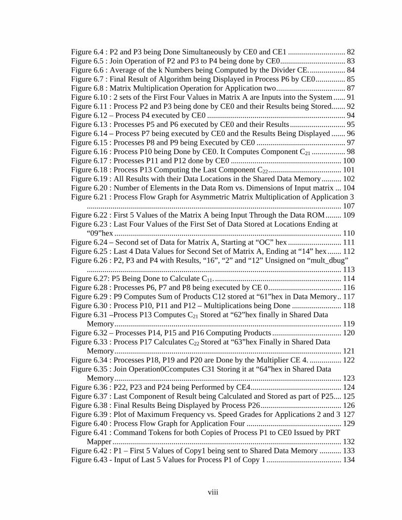
Figure 6.4 : P2 and P3 being Done Simultaneously by CE0 and CE1 ............................. 82 Figure 6.5 : Join Operation of P2 and P3 to P4 being done by CE0................................. 83 Figure 6.6 : Average of the k Numbers being Computed by the Divider CE................... 84 Figure 6.7 : Final Result of Algorithm being Displayed in Process P6 by CE0............... 85 Figure 6.8 : Matrix Multiplication Operation for Application two................................... 87 Figure 6.10 : 2 sets of the First Four Values in Matrix A are Inputs into the System ...... 91 Figure 6.11 : Process P2 and P3 being done by CE0 and their Results being Stored....... 92 Figure 6.12 – Process P4 executed by CE0 ...................................................................... 94 Figure 6.13 : Processes P5 and P6 executed by CE0 and their Results ............................ 95 Figure 6.14 – Process P7 being executed by CE0 and the Results Being Displayed ....... 96 Figure 6.15 : Processes P8 and P9 being Executed by CE0 ............................................. 97 Figure 6.16 : Process P10 being Done by CE0. It Computes Component C21 ................. 98 Figure 6.17 : Processes P11 and P12 done by CE0 ........................................................ 100 Figure 6.18 : Process P13 Computing the Last Component C22..................................... 101 Figure 6.19 : All Results with their Data Locations in the Shared Data Memory.......... 102 Figure 6.20 : Number of Elements in the Data Rom vs. Dimensions of Input matrix ... 104 Figure 6.21 : Process Flow Graph for Asymmetric Matrix Multiplication of Application 3
................................................................................................................................. 107 Figure 6.22 : First 5 Values of the Matrix A being Input Through the Data ROM........ 109 Figure 6.23 : Last Four Values of the First Set of Data Stored at Locations Ending at
“09”hex ................................................................................................................... 110 Figure 6.24 – Second set of Data for Matrix A, Starting at “OC” hex ........................... 111 Figure 6.25 : Last 4 Data Values for Second Set of Matrix A, Ending at “14” hex ....... 112 Figure 6.26 : P2, P3 and P4 with Results, “16”, “2” and “12” Unsigned on “mult_dbug”
................................................................................................................................. 113 Figure 6.27: P5 Being Done to Calculate C11. ................................................................ 114 Figure 6.28 : Processes P6, P7 and P8 being executed by CE 0..................................... 116 Figure 6.29 : P9 Computes Sum of Products C12 stored at “61”hex in Data Memory.. 117 Figure 6.30 : Process P10, P11 and P12 – Multiplications being Done ......................... 118 Figure 6.31 –Process P13 Computes C21 Stored at “62”hex finally in Shared Data
Memory................................................................................................................... 119 Figure 6.32 – Processes P14, P15 and P16 Computing Products ................................... 120 Figure 6.33 : Process P17 Calculates C22 Stored at “63”hex Finally in Shared Data
Memory................................................................................................................... 121 Figure 6.34 : Processes P18, P19 and P20 are Done by the Multiplier CE 4. ................ 122 Figure 6.35 : Join Operation0Ccomputes C31 Storing it at “64”hex in Shared Data
Memory................................................................................................................... 123 Figure 6.36 : P22, P23 and P24 being Performed by CE4.............................................. 124 Figure 6.37 : Last Component of Result being Calculated and Stored as part of P25.... 125 Figure 6.38 : Final Results Being Displayed by Process P26......................................... 126 Figure 6.39 : Plot of Maximum Frequency vs. Speed Grades for Applications 2 and 3 127 Figure 6.40 : Process Flow Graph for Application Four ................................................ 129 Figure 6.41 : Command Tokens for both Copies of Process P1 to CE0 Issued by PRT
Mapper .................................................................................................................... 132 Figure 6.42 : P1 – First 5 Values of Copy1 being sent to Shared Data Memory ........... 133 Figure 6.43 - Input of Last 5 Values for Process P1 of Copy 1...................................... 134

ix
Figure 6.44 : Two Command Tokens being Issued to PRT Mapper for Copy 1............ 135 Figure 6.45 : Command Tokens Issued to CE0 and CE1 by PRT Mapper for Copy1 ... 136 Figure 6.46 : Instructions for Process P1 of Copy 2 and for Process P3 of Copy 1 ....... 137 Figure 6.47 : Two Command Tokens Issued to PRT Mapper for Copy 2...................... 139 Figure 6.48 : Two Command Tokens Issued to CEs by PRT Mapper for Copy 2 - P2 and
P3 ............................................................................................................................ 140 Figure 6.49 : Process P3 for Copy2 of the Application .................................................. 141 Figure 6.50 : Division Operation in the Process of Execution. ...................................... 142 Figure 6.51 : Division Operation for Process P5 with Results and Issue of Command
Token to PRT Mapper for Copy 1 .......................................................................... 144 Figure 6.52 : Command Token for Process P4 Issued to PRT Mapper and from PRT to
CE4 for Copy 1 ....................................................................................................... 145 Figure 6.53 : Multiplication Operation by CE4 and Command Token Issued to PRT
Mapper for Copy 1.................................................................................................. 147 Fig: 6.54 : Command Token for P5 Issued to PRT mapper and from PRT to CE2 for
Copy 1..................................................................................................................... 148 Figure 6.55 : Process P5 and Command Token to PRT Mapper for Copy 2.................. 149 Figure 6.56 : Join Instruction for Process P6 of Copy 1................................................. 151 Figure 6.57: Instruction for P7 and Final Results for Copy1 of Application Displayed 152 Figure 6.58 : Result of Multiplication and Command Token Issued to PRT Mapper.... 154 Figure 6.59 : Join Process P6 - Instructions for Copy 2 ................................................. 155 Figure 6.60 : Process P7 with Final Value of the Result Displayed for Copy 2............. 156 Figure 6.61 : Process Flow Graph for the Application Swapping Two Sets of Values.. 158 Figure 6.62 – First 2 Values being Input from Input ROM into the Shared Data Memory
................................................................................................................................. 161 Figure 6.63 : Values of k and Safe Values of T1 and T2 being Input into the System .. 162 Figure 6.64 : Instructions for Processes P2 and P4......................................................... 164 Figure 6.65 : Process P3 being done. First Comparison Will be Performed. ................. 165 Figure 6.66 : Process P5 is done comparing 60 with 90................................................. 166 Figure 6.67 : P2 being Re-Executed as Part of First Feedback Loop ............................. 168 Figure 6.68 : First Feedback for P4 done by CE0........................................................... 169 Figure 6.69 : Process P3 being Executed For the Second Time ..................................... 170 Figure 6.70 : Process P5 being Executed Second Time and the Follow on Process P4 . 172 Figure 6.71 : Process P2 Executed 3rd Time and a Value of 90 Stored at Location x”03”
................................................................................................................................. 174 Figure 6.72 : Process P4 Executed 3rd Time With 70 Stored at Location x”04”............ 175 Figure 6.73 : Process P3 Executed 3rd Time Where 90 is Compared with 100.............. 176 Figure 6.74 : Process P5 done by CE0 where 70 is compared with 60 .......................... 177 Figure 6.75 : Process P2 Executed 4th time by CE1 to Obtain a Result of Unsigned “100”
................................................................................................................................. 178 Figure 6.76 : P4 is done by CE1 - 4th Iteration. A Value of Unsigned “60” at x”04” ... 179 Figure 6.77 – Process P3 Final Execution and Token for P6 Issued to PRT Mapper .... 180 Figure 6.78 – Process P5 Executed for Last Time and Command Token for P6 ........... 182 Figure 6.79 – Join Operation P6 with Final Results and Addresses Displayed.............. 183

1
Chapter One Introduction
1.1 Background
Despite the increase in computing power and performance of uni-processor
systems, there have been advancements in technology causing the evolution of complex
real and non real time algorithms which demand the increased performance of
multiprocessor systems. Along with such requirements, is the need for a fault tolerant, re-
configurable system, which can dynamically reconfigure to match the needs of compute
intense applications. Such systems often use Field Programmable Gate Array (FPGA)
technology as the basis for their use and design. The ability to configure these chips for a
particular application and then quickly modify a configuration to meet the demands of
new applications is highly desirable. Not only does it allow for application specificity,
but it can also add a certain degree of fault tolerance and re-configurability that
applications may demand. If a particular section of the chip has a fault then the existing
logic can still be modified to execute the applications on the chip.
An early inception of these concepts originally led to introduction of a tightly
coupled Dynamic Pipeline Computer Architecture (DPCA) [1,2,3,4,5,6,7,8,9] in the early
1980s. The DPCA as originally envisioned was reconfigurable at the application and the
node level. It was reconfigurable at the application level in the sense that it could execute
any application described by a process flow graph. At the node level, the architecture
could dynamically allocate additional processors, on the fly, to a processor node when it
became overloaded and continue execution of the application, as described in [3]. As
indicated in [3], The DPCA architecture was originally developed as a real time
processing system for phased array radar. In addition, the system was designed to
execute any medium to coarse grained application which could be modeled as a single or
multiple input/output, cyclic or acyclic process flow graph of any topology. The
architecture varied from most others at the time because of utilization of hybrid data-flow
concepts and von Neumann type processors. It was a hybrid data flow machine since it
used data flow concepts to migrate data from one process to another but still made use of
a program counter in the actual execution of processes on processors. Additionally,

2
within the architecture, it is not the arrival of data at a node which causes the processes to
execute but instead the arrival of a control token. The idea was to implement a medium
to coarse grained multi-processor system with no inter-communication between
individual processors. This system would consist of multiple processors that would
communicate only through the exchange of command tokens and shared data memory.
These tokens, upon their arrival into a queue fronting a processor would activate an
appropriate process in the instruction memory of a given processor, commonly referred to
in the architecture as a Computing Element (CE). A functional level diagram of the
original DPCA is shown in Figure 1-1. Each CE in the figure was to be an early 1980s
era mini computer.
The DPCA architecture functioned by receiving any process flow graph as an
input. The Operating System would analyze this flow graph and allocate processes to
CE's that would optimize the flow graph's execution [3,4,10,11]. The system would then
be initialized and the application execution would start. Throughout an application's
execution, control tokens circulate in the system. As a processor executing in a CE
completes, it writes data needed by successor processes of a flow graph to the shared data
memory of Figure 1.1. It lastly generates a control token which is routed to the CE-
Mapper Process Request Token (PRT) Router and then the Process Request Mapper
functional unit of Figure 1.1. The Process Request Mapper, using hardware; dynamically
balances the load of the system. The CE-Mapper PRT Router and Process Request
Mapper analyze the current load condition of each CE and issue a control token to a CE
holding a copy of the process where wait time for execution of the process is minimal
[3,7,12]. A CE receiving a control token executes the desired process and then, upon its
completion, issues a control token to the CE-Mapper that indicates the next process (es)
to execute. In this system, CE's do not directly communicate but are able to share data
through the CE-Data Memory Circuit Switch [2,3,8,9,27,28]. Applications are thus
executed by executing the process flow graphs that represent them.

3
For a more intricate explanation of the DPCA system and its operation, see [3].
Figure 1.1 : High Level Architecture of the DPCA
TOKEN

4
The DPCA system, over time and as Integrated Circuit (IC) technology changed, has
evolved into the single-chip based HDCA or the Hybrid Data/Command Driven
Architecture.
1.2 HDCA Concepts
As one can see upon review of [1-12], high level simulation and design for
several of the functional units of the DPCA system were developed but no hardware
prototypes were ever developed for experimental testing. Also, no attemps were made to
prototype and test the entire DPCA system. More recently, due to rapid enhancement in
IC technology and heightened interest in high performance single-chip multiprocessor
architectures for embedded and other applications, it was realized that the DPCA was
functionally amenable; with some functional changes and enhancements to being
implemented as a hybrid single-chip heterogeneous multiprocessor system.
Consequently, the DPCA system has evolved into the current HDCA system. The start
was in the 1997 time-frame [13,14]. A number of changes were incorporated while
moving from the DPCA to the HDCA system. Amongst the most significant were,
moving from a distributed system to a single chip architecture or a System On a Chip
(SoC) and making the system reconfigurable at a third, processor architecture level,
which basically implied that the processor used in a Computing Element (henceforth
referred to as a CE), could be dynamically configured from a reference “library” of
processors to optimize execution of portions of the process flow graph. The entire HDCA
concept was envisaged to be implemented in a three stage process. As part of the first
stage, system simulation work [13,14], it was demonstrated that the system could be
reconfigured at the system and node levels. A hardware prototype was not built at that
time due to constraints related to costs and changes in architecture that were to come.
Recent changes in IC technology have spawned reconfigurable logic such as FPGAs with
as many as 5 to 6M gates on a single chip and have also scaled down the costs associated
with manufacturing such chips. An approach was undertaken of first imeplementing and
experimentally testing and validating an FPGA based hardware prototype of key
functional units of the HDCA [15,16]. A first hardware prototype of a very basic and
scaled down entire system HDCA was developed, experimentally tested and it further

5
validated that the architecture could execute simple and elementary applications
described by acyclic process flow graphs [17].
As a background to which the research and development of this thesis can
be compared, an examination of various journals and papers reveals different interesting
areas to which reconfigurable and dynamic computing has expanded. One of these areas
is in developing custom architectures. In [18], the researchers show that a custom FPGA
solution outperforms an ASIC based design due to the fact that the logic in an FPGA can
be reconfigured to meet the needs of applications running on the architecture.
Another area of research is in replacing software modules by the equivalent
hardware circuitry. It is here that the reconfigurable nature of an FPGA is most important
as shown in [19], where one can use the available hardware resources in the FPGA to
accelerate the bottleneck in the software code, thereby gaining some extra performance
benefits. Since the logic elements in the FPGA are programmable, one can customize the
hardware for any application without having the need to make board revisions. Also, the
work done in [19,20,21] show that often implementing an algorithm in hardware instead
of software provides performance improvements.
Recently, combining ASICs with reconfigurable logic has been increasing as
shown in the GARP system of [22,23]. Here the researchers allow the system to
implement certain functions of an application in the reconfigurable logic in order to
obtain enhanced performance. The close integration of ASICs and reconfigurable logic
allows designers to take advantage of fast, general purpose ASICs while maintaining the
flexibility and specificity of reconfigurable logic.
Yet another area where reconfigurable computing is expanding is in space
applications where the focus is on fault tolerant, low power, radiation tolerant design. In
the work done in [24], the researchers have been designing a Reconfigurable Data Path
processor for Space applications where execution agility is maintained by conditional
switching of the data path instead of conditional branching.
Another venture is in the work done at Clemson University [25] where scientific
algorithms are mapped to FPGAs through the use of a 'toolbox' of designs. The
Reconfigurable Computing Application Development Environment (RCADE) system
combines several designs from its library to execute an application in a data flow manner.

6
Through the use of these techniques, the researchers are able to utilize FPGAs for
scientific applications while maintaining the desired speed of the application.
The work done in [26] is notable, where the researchers present a coarse-grained
dynamically reconfigurable array architectures promising performance and flexibility for
different challenging applications in the area of broadband mobile communication
systems.
Based on the above developments, the HDCA can be classified under the same
category as the work reported in [21, 25 and 26]. Reconfigurable Architectures have thus
touched every aspect of life from Communication, Signal Processing to Space
applications in the recent years. Unlike systems in the work of [21,25], the HDCA system
can analyze an input application's needs at run time and then configure the system for the
most efficient execution. Additionally, the HDCA is designed to be fault tolerant. It is
capable of recognizing failed nodes and reconfiguring itself to continue operations.
Overall, the main contributions to this field are the integration of compiler-type run time
system configuration, with dynamic hardware implementations of software algorithms
and the incorporation of fault tolerance. Typical applications of the HDCA architecture
would thus be in real and non-real time systems, such as in embedded systems for use in
space, phased array radars, and sonar signal processing and different areas of Digital
Signal Processing such as image processing where multiple filtering operations may be
needed to be performed on the same set of input pixels. As an example, one set of the
input data pixels in an image may need to be Sobel edge enhanced and the other may
need to be smoothened.
1.3 Goals and Objectives of the Thesis
The main goal of the research and development done here is to design,implement
and test a second phase functionally working latest model of the HDCA computer
architecture[3,12,13,14,15,16,29] with non complex and complex applications and take it
through a “virtual prototyping” process where a working single-chip post place and route
VHDL simulation model is demonstrated. In order to achieve this goal, several
previously developed system functional units will be used. Some will be significantly
modified and newly designed.A VHDL model of the latest version of the HDCA will be
developed.The system should have multiple Computing Elements (each with a Multi-

7
function Queue [16]), the Process Request Token Mapper [15], a shared memory that is
accessible by all processing elements [29], and a common Token Bus. An additional goal
is to demonstrate the ability of the system to function with heterogeneous processing
elements and to reconfigure dynamically at the node level at run-time to meet the
additional processor work load requirements and maintain a fault tolerant model of the
system (as mentioned in [3]). Thus the work done here, should demonstrate that the
architecture can process an application dynamically reconfigurable at the node level. The
second phase virtual prototype of the HDCA will not have the restriction of the first
phase system prototype [17] which was that one process could, fork into, atmost two
processes. Removing this restriction will allow the HDCA to execute interesting process
flow graphs, such as the acyclic graph shown in Figure 1.2 below.
Figure 1.2 : Process Flow Graph for a Typical Application
Finally, the work of this thesis demonstrates that the heterogeneous shared
memory HDCA multiprocessor system can be implemented to a single-chip.
1.4 Thesis Summary
The remainder of the thesis provides the detailed information on the HDCA
system architecture and the steps taken to functionally enhance and upgrade the existing
model to one which can implement process flow graph of any topology and implement
node level dynamic reconfigurability. Chapter Two adresses previous work done on the
HDCA and provides more detail on the system concepts utilized for the same and

8
explains in great detail, all the core components of the system including the additional
components added while moving to the second phase model of the HDCA. Chapter Three
provides information on the systematic design methodology utilized and the changes
made to the first phase prototype [17] to get it from a partially-functional condition to a
fully functional, synthesizable and implementable second phase “virtual prototype” using
the latest version of the Xilinx ISE 6.2.3i software [30] and Mentor Graphics Modelsim
5.7g SE [31] tool sets.in the new foundation ISE environment. Chapter Four addresses
the “Virtual Prototype” development process and provides information on hardware
usage and timing statistics. Chapter Five introduces the functional enhancements into the
HDCA and provides a detailed insight into the concepts of dynamic node level
reconfigurability and multiple forking. Next, Chapter Six discusses complex real/non-real
time applications developed for the architecture and the simulation results obtained. It
also showcases talks about system scalability at the application level and performance
results. It also justifies the policy decisions taken in the process of demonstrating the
concepts. Chapter Seven concludes by discussing the overall achievements and suggests
directions for the continued advancement of the architecture in the form of
recommendations.

9
Chapter Two Background and System Details
2.1 HDCA and Related Background Work
The HDCA architecture as developed and demonstrated in [17] consisted of three
CE’s (each with an instruction memory and CE controller), a Token bus, a Process
Request Token (PRT) mapper with controller and a data bus with shared data memory as
shown in Figure 2.1a. In theory, the CEs used in the system could be any CEs but in
order to demonstrate the heterogeneous nature of the system, two of the CEs used were
16 bit un-pipelined memory register type computer architectures developed as part of
coursework. The third CE was a special purpose Divider CE.It was different in the sense
that it did not have a program counter like the other CE instead it used a controller along
with a special purpose pipelined divider to execute processes that needed to use the
divide operation.
One of the core concepts of the HDCA architecture is its ability to execute any
application that can be described by a process flow graph model. As mentioned in [17], in
this model, data arrival does not trigger process execution as would a pure data flow
graph model. Instead, the arrival of Control Tokens triggers process execution. These
Control Tokens are shorter and thus more efficiently and quickly transmitted between
computing elements than blocks of data. In the process flow model, data is propagated
from one process to another through the use of a shared memory structure. Actions are
performed on that data when processes access the data memory. The HDCA architecture
operates on the principle that applications can be modeled using process flow graphs and
then implemented in a system.
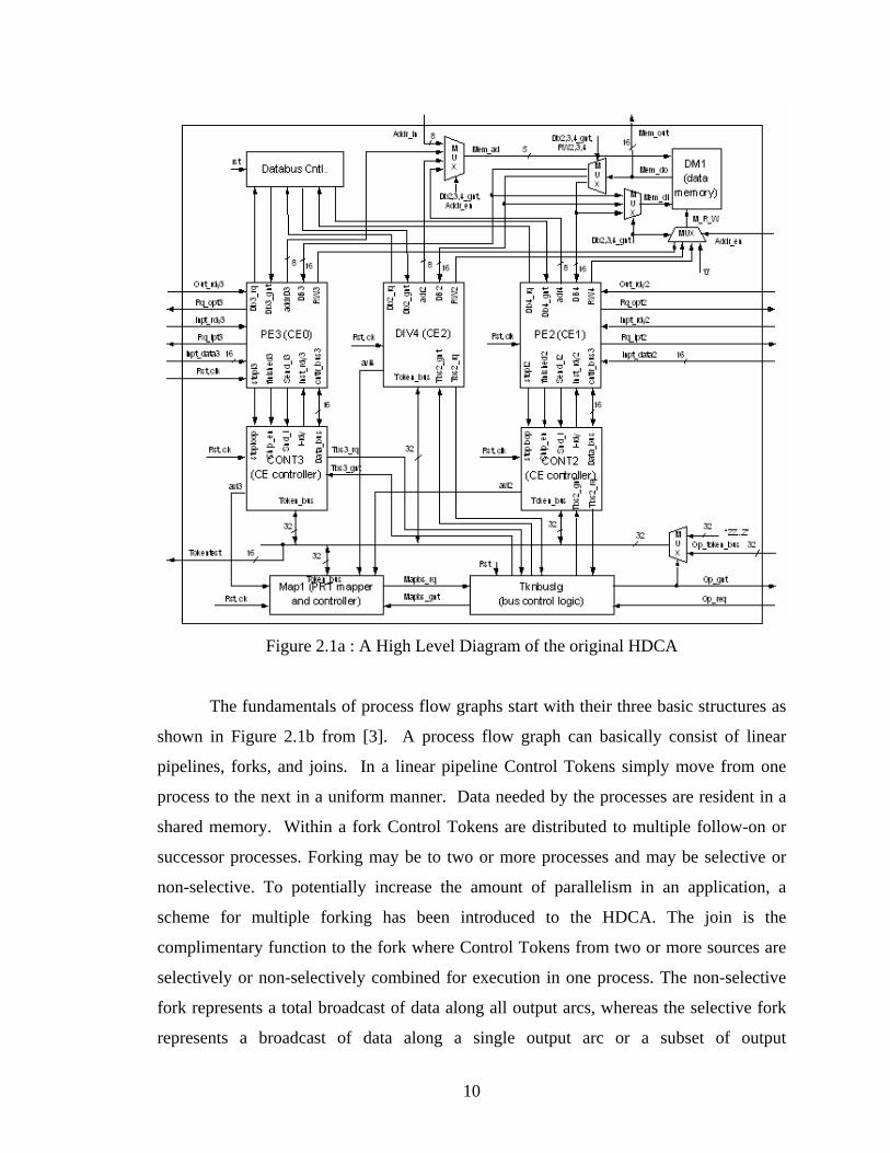
10
Figure 2.1a : A High Level Diagram of the original HDCA
The fundamentals of process flow graphs start with their three basic structures as
shown in Figure 2.1b from [3]. A process flow graph can basically consist of linear
pipelines, forks, and joins. In a linear pipeline Control Tokens simply move from one
process to the next in a uniform manner. Data needed by the processes are resident in a
shared memory. Within a fork Control Tokens are distributed to multiple follow-on or
successor processes. Forking may be to two or more processes and may be selective or
non-selective. To potentially increase the amount of parallelism in an application, a
scheme for multiple forking has been introduced to the HDCA. The join is the
complimentary function to the fork where Control Tokens from two or more sources are
selectively or non-selectively combined for execution in one process. The non-selective
fork represents a total broadcast of data along all output arcs, whereas the selective fork
represents a broadcast of data along a single output arc or a subset of output

11
arcs.Similarly, during the execution of a selective join, only a selected subset of input
arcs to a process is active. A non-selective join is triggered when all the inputs to a
process are active. When these basic structures are combined, any application composed
of multiple processes can be modeled. Figure 2-2 shows a simple process flow graph of
an algorithm operating on integers. In this graph execution begins at “Process P1” with
the input of a set of integers. “Process P1” then forks a subset of this information to
processes P2 and P3 where some integers are summed. Simultaneously, in pipeline
fashion, Process P1 inputs a second set of integers. Processes P4 and P5 then perform
multiplication and division operations on their results to obtain new results which they
transmit to process P6 where an absolute difference is taken. Process P7 finally outputs
the result of this computation to the user. The simulation results and virtual prototype
output waveforms for this application can be found in later chapters of this thesis. The
idea behind the HDCA is to have multiple processors
Figure 2.1b : Basic Process Flow Graph Structures.
Processes on individual Computing Elements (CE's) do not start execution until an
initializing token has arrived. Once a token is received, indicating the location and
availability of data needed by the process, the CE parses it in order to determine the
proper process to execute. This is due to the fact that each CE can hold several processes
in its Instruction memory or only one process. The CE then executes the appropriate
process and upon completion issues the follow-on token(s) for the successor process (es).

12
These tokens are the sole communication between CE's. . An example Control Token
format is shown in Figure 2.3.
Figure 2.2 : Example Process Flow Graph.
In this token the Hold Field is used to indicate a requested process that is a
member of a join operation. It is also used by the system in a manner such that the
processor token queue depth represents true wait time for the initiation of a requested
process. The Physical address denotes the destination CE or functional unit for the token.
For example the five different CEs used in the HDCA system presented later have
addresses of two, three, four, five and six The Process Number indicates which process to
execute and the Data Location provides the address of the data in shared memory which
is accessed through the Crossbar interconnect switch as described in [29,32].
Hold Field &
Physical Address Process Number Data Location
Figure 2.3 : Token Format for the HDCA
2.2 PRT Mapper
An important function of the PRT Mapper (see Figure 1.1 for this dunctional unit in the
DPCA and Figure 2.4 for a more detailed view of its design as enhanced to operate in the

13
HDCA) is to maintain the dynamic system workload balance. In order to achieve this
goal, it constantly monitors the input control token queue lengths/depths of each CE in
order to determine the most available CE. Control tokens are sent first to the PRT
mapper where it is cross-referenced in a RAM table to determine which CE's are able to
run the desired process. Not all CEs can run all the processes. The workloads of the
eligible CEs are then compared, resulting in a control token being issued to the least
loaded CE i.e the one with the lowest amount of work to be done. In order to determine
which CE has the least amount of work, the concept of shortest wait time is used. The
CE that has the shortest wait time indication in its input control token queue is the most
available since it will service the token before its corresponding CE. Once the eligible
CE's are known, it compares the workloads of those CE's to determine which is the least
utilized. A new control token is then created using the physical address of the selected
CE and the location of the associated data. The newly formed token is then output on the
Token Bus via the OBUS to the appropriate CE. This new control token contains the
Process Number to be executed, the physical location of the destination CE, and the
address of the required data in the shared data memory. The original design capture was
done in Verilog, therefore it was necessary to interpret the code and translate it to VHDL
for the HDCA VHDL model. This was done in the work described in [17].
In addition to the load balancing function of the PRT mapper, the state of the
system is continuously monitored in order to detect faults and system failures. If a CE
node fails, the system has the ability to shift the work of a failed node to another location.
Additionally, the system is designed with the intent to allow it to reconfigure its
processing elements in the event of a failure or to create additional copies of a resource
that is heavily used. This happens when the tokens have been queued sufficient enough,
that the queue depth reaches a pre-defined “threshold” determined by the user/operating
system. At this stage, an additional processor is dynamically initiated and configured, on
the fly, to “help-out” this overloaded CE and help it reduce the queue depth by executing
some of the follow on processes. This allows the system to dynamically maintain the
desired application system input to output rate and functionality of the system even if
elements fail or workloads are higher than initially and statically predicted from the
application process flow graph.

14
Figure 2.4 : Process Request Token mapper Circuit Diagram.

15
2.3 Multi-Function Queue
When the original architecture (DPCA) was designed as represented in Figure 1-
1, it was a known fact that the CE's would each require a FIFO queue to hold control
tokens that were yet to be parsed and executed. This was so because as tokens are parsed
by the CEs and a particular CE gets busy executing the process, the incoming tokens have
to wait for their turn in the queue. If there was no queue provided, these tokens would be
lost and hence the system would not behave as expected. Gradually, as work progressed
on the development of the HDCA, it was determined that this queue needed some more
additional features. These new features allow the HDCA to operate in both a real time
and non-real time environment, and they support its dynamic node-level re-
configurability. The functionality of the FIFO queue was expanded to implement six
different functions [16]. It can read and write simultaneously, maintain a count of
elements in the queue, and signal when a programmable queue depth threshold is met. It
can also switch the order of any two tokens in the queue and report the net rate at which
tokens are entering or leaving the queue over a programmable time period. A high-level
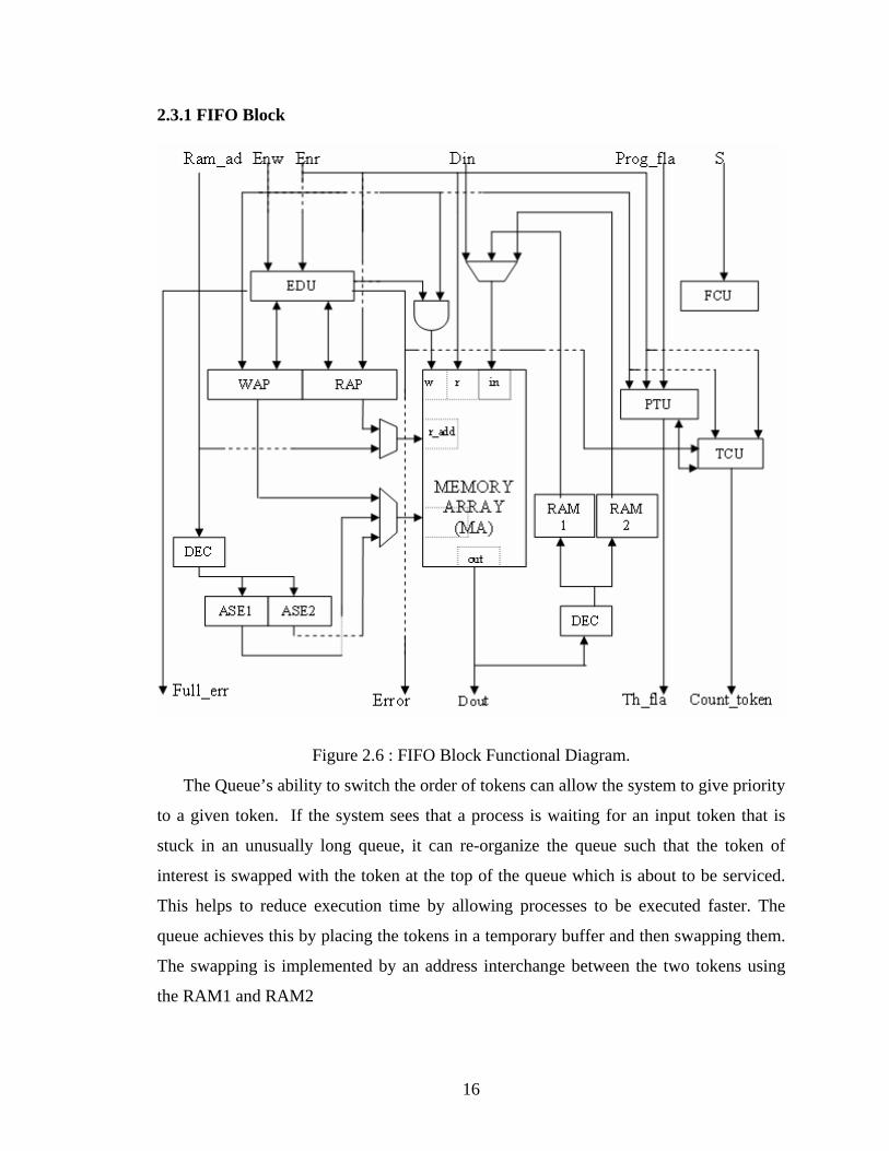
block diagram of the Multi-Function Queue is found in Figure 2-5. Figures 2-6 and 2-7
show a functional level diagram of the FIFO and Rate blocks respectively.
Figure 2.5 : Multifunctional Queue
16
2.3.1 FIFO Block
Figure 2.6 : FIFO Block Functional Diagram.
The Queue’s ability to switch the order of tokens can allow the system to give priority
to a given token. If the system sees that a process is waiting for an input token that is
stuck in an unusually long queue, it can re-organize the queue such that the token of
interest is swapped with the token at the top of the queue which is about to be serviced.
This helps to reduce execution time by allowing processes to be executed faster. The
queue achieves this by placing the tokens in a temporary buffer and then swapping them.
The swapping is implemented by an address interchange between the two tokens using
the RAM1 and RAM2

17
2.3.2 Rate Block
Figure 2.7 : Rate Block Functional Diagram.
Another important feature of the Queue is the "rate" feature as represented by the
Rate Block of Figure 2.7. It measures the Input Token Rate Change (ITRC) over a
programmable time interval (Time_S). This time period indicates the time period over
which to base the calculations. The Queue then determines whether there was a net
increase or decrease in the number of tokens passing through the Queue over the given
time period. The outputs of this function are a sign bit (Sign) and a magnitude (ITRC).
Thus the Operating System can determine the workload of a CE by the number of tokens
arriving or departing a given queue. The original queue VHDL code had to be modified
as reported in the work done in [17,33] to suit the HDCA system.

18
2.4 The Computing Elements
The first phase prototype of the HDCA consisted of 3 Computing Elements [17,
33]. Two of the CEs - CE0 and CE1, were 16-bit unpipelined memory-register computer
architectures, developed as part of the graduate program coursework and as shown in
Figure 2.8. In order to show the heterogeneous nature of the system, a special purpose
simple pipelined divider CE was also included in the system. The instruction set for CE0
and CE1 is shown in Table 2.1. Both processors have full functionality: a register set in
the data path available to the assembly language programmer, a Hardware Vectored
Priority Interrupt System (HVPIS) in addition to other functional units such as Arithmetic
and Logical Unit (ALU), a Program Counter (PC) and simple Input/Output (I/O)
structure. The instruction set listed in table 2.1 was felt to be sufficient to test the
functionality of the second phase model of the HDCA. The processor used for CE2 is a
simple pipelined divider circuit. This divider can be considered as a special purpose
circuit for a system that needs additional computational power and it allows the single-
chip multiprocessor prototype system to be heterogeneous. Each CE, as shown in Figure
2.8, has its controller, which includes a multifunctional queue [16,17,33], a Lookup Table
(LUT) and an Interface Controller (see Figure 2.9 for the CE controller). Additionally, as
part of work done to build the second phase model, two additional Computing Elements
were added to the HDCA system. In order to execute complex and non-complex
applications, the need for a special purpose multiplier CE was felt. Often, in DSP and
Image Processing applications, multiplication is an important aspect of any operation and
hence a new special purpose multiplier was added to the HDCA system. A fifth CE will
be added to this HDCA system as part of this work and it will be architecturally the same
as the Memory-Register CEs of Figure 2.8., but it is unique in the sense that it does not
come into picture under normal conditions. Under normal operating conditions, when the
Queues of the existing CEs have not built up to their threshold, this CE acts as a stand-by
CE monitoring the queue depth of either of the two CEs. Once the queue depth of both of
the operational CEs exceeds the pre-programmed threshold, this additional CE is
dynamically configured, on the fly, to initiate and start accepting the tokens from that
point on and executing them. This concept has been explained in detail in Chapter 5
along with the design decisions that have been made. Implentation of this concept results

19
in node-level dynamic capability of the architecture. Once the queue depth goes reduces
below the pre-programmed threshold, the CE goes back to its sensing state where it
silently monitors the queue depth of either CEs.
Table 2.1, Instruction Set of the Memory-Register CEs
No. Instruction Action
0 Mem [Ri] <= input Input data to Mem [Ri], i = 0,…3
1 Add RD, Mem [Ri] RD <= Mem [Ri] + RD, i = 0,…3, D = 0,…3,
D≠i
2 Store Mem [Ri], RD Mem [Ri] <= RD, i = 0,…3, D = 0,…3, D≠i
3 Jump address immediate PC <= Address immediate
4 Branch RD, Mem [Ri],
Address
If RD >= Mem [Ri], then PC <= Address, i =
0,…3, D = 0,…3, D≠i
5 Sub Mem [Ri], RD Mem [Ri] <= Mem [Ri] – RD, i = 0,…3, D =
0,…3, D≠i
6 Output <= Mem [Ri] Output data Mem [Ri], i = 0,…3
7 Load RD, Mem [Ri] RD <= Mem [Ri], i = 0,…3, D = 0,…3, D≠i
8 Branch out loop If RD = Mem [Ri], then branch out Process flow
loop, i = 0,…3, D = 0,…3, D≠i
9 Load Ri, immediate Ri <= Immediate
A Increment Ri Ri <= Ri +1, i = 0,…3
B Add Ri, immediate Ri <= Ri + immediate, i = 0,…3
C Sub Ri, immediate Ri <= Ri – immediate, i = 0,…3
Additionally, this new CE can also be configured with proper programming to act
as a back-up CE in case any node fails due to unforeseen circumstances. This would help
in producing a fault tolerant model of the system, consistent with the idea presented in
[3].

20
Most of the instructions represented by Table 2.1 are self explanatory. The special
instruction “Branch out Loop” is used to exit from applications that involve looping and
it is necessary to exit from the loop when a predefined condition has been met. This is
further explained in the CE controller module.
P C
R 5
R 4R 0
R 1
R 2
R 3
IR 0IR 1
MA
R
S h ifte r
A L U
M u x
M u xM u x
D ec o d er
C o n tro lle r
V ec to rIn te rru p tS y stem
M u x
In s tru c tio nM em o ry
1 2 8 x 1 6 b i tMux
A d d re ss B u s
D a ta B u s
In p u t L in e s
In p u t R e a d y
O u tp u t R e a d y
Figure 2.8 : Memory Register Computer Architecture - CE0 and CE1
The HVPIS and IR1 are not used in the cirtual prototype testing of the HDCA reported in
this thesis. These units are though included in the design and VHDL description of the
CE and can be used whenever desired.

21
2.5 The CE Controller
Figure 2.9 : CE controller for 16-bit unpipelined Memory Register CEs
Each Memory register CE architecture has a controller associated with the CE as
shown in Figure 2.9. It basically consists of an Interface Controller, the FIFO queue and a
Look up Table (LUT). Some of these components have been described earlier in this
chapter. The LUT contains all the information necessary to communicate with a CE.
During system initialization, the LUT is loaded with information about all of the
processes that a given CE can execute. It consists of process number identifier (PN), the
address of the Process Number’s first instruction in memory (Instruction Location),
follow-on process numbers (PN0, PN1), a hold bit (H) and a join bit (J). Since the only
communication between CE's is tokens, any CE must know what the next processes are
in order to issue the correct follow-on token. This explains the reason for having the
follow on process numbers in the LUT. The functionality of Hold and Join bits come into
picture when the process flow graph is non-linear, or in other words, has forks and joins
as explained earlier. The Hold bit is set to logic one if the follow-on process to be
executed is a member of a Join operation. The Join bit when set to logic one indicates that
the Process to be run is a join process and thus will have more than one token associated
with it in the Queue. To further explain, let’s take a simple example. Say process P1 forks

22
into two follow on processes, P2 and P3 and let’s say these processes finally join at P4 as
illustrated in Fig.2.10.
Figure 2.10 : Explanation of Hold and Join Concept
The initial HDCA design [17,33] was limited to two follow on processes but in the work
done here it will been shown that the design can be modified to incorporate a multiple
fork where a single process has more than two successors. Also the number of processes
that could be held in the LUT is limited to 18 processes. This is, however, a figure that
can be changed and is a function of the underlying technology to which the design is
being synthesized and the complexity of the application. Once the LUT is loaded, it
works by receiving a token from the Queue. It compares this token's Process Number
with the LUT entries. In the event of a match, its instruction buffers are then filled with
the Instruction address and the data address. This helps the CE decide what is to be done.
An example of these instructions is as follows. Instruction '0' tells the CE to load the data
address into a register. If this is a join operation, then Instruction Two loads data address
two into a register. Instruction one tells the CE to jump to the address of its first
instruction. The LUT sends these instructions when the CE indicates over the 'Finished'
input that it is done executing the current process and is ready to receive information
about the next process that is to be executed. This is explained more vividly in Chapter 6,
when applications are discussed. When the CE finishes a previously running Process, it
signals 'Finished' and thus the LUT prepares to send the follow-on token to the PRT
mapper, it places the finished Process' information in a buffer (Last PN, Time Stamp,
Data Address). Then it compares the Process Number with the entries in its table. Once a
P1
P2
P3
P4
Hold bit =1
Hold bit =1
Join bit =1

23
match is found, it sends the data location along with the Hold Field bit, and the follow-on
Process Number(s) to the Interface Controller, which sends the token(s) out on the Token
Bus.
2.6 Interface Controller
The Interface Controller of Figure 2.11 provides the logic to integrate the LUT, the
Queue, and the CE. One of the functions of the Interface Controller is to receive Tokens
from the Token Bus and transmit output Tokens. On the receive side, it has the
previously described FIFO buffer to temporarily hold fifteen inbound tokens. Besides this
simple task, the Interface Controller is a State Machine for the control of the LUT and
Queue. The State Diagram for the Interface Controller is found in Figure 2.11
SystemReset
LoadTable
GetToken
PRAM
CheckStatus
DummyRead
SendPRT
DeQeue
IssueStopLoop
RST =1
LUT not fullX < 10000
X = 10000
Instr = Load table
Del
ay =
true
Inst
r = S
witc
h to
ken
Delay = false
Bus grant = 0
Instr = Check Status
Bus grant =1
Finished = 1
Cnt > 0
Nxt_lded = 0 Cnt > 0
Finished = 0
WR_out=”01”or “00” or “11”
Nxt_lded = 1
Comp = true or
bus_grant = ‘0’R_L_Tab
le = “00”
or “01” o
r “10”
Finished=1, nxt_lded=0
running=true
Nxt_lded = 1
Nxt
_lde
d=0 N
xt_lded=0
Stop_flag=FALSE,
nxt_lded=1, finished=1
Stop
_fla
g=TR
UE,
nxt_
lded
=1, f
inis
hed=
1
Token Rcvd
Load threshold & time
Cnt = 0
Figure 2.11 : Interface Controller State Machine for the CE
The controller starts functioning, as soon as the reset signal goes active low. The
first state, after “System Reset” is the “Load Table” state. It remains in this state until the

24
Look up Table described above has all its entries populated. How many entries are
needed to fill up the Look up Table - depends on the topology of the process flow graph.
This concept is thoroughly explained in Chapter 6 where applications are described. Once
the Look up Table is full, the controller moves to the “Get Token” state. Here the
controller waits for properly addressed tokens to arrive from the Token Bus. The first
thing the controller checks is if a process previously sent to the CE has completed
executing. If it has, and another token is available in the instruction buffers for execution
(Next_Loaded is true), then the state switches to Send PRT. If no token is ready for
execution, then the state moves to the Dummy Read State. If the CE is still busy
executing a process and a token is in the queue, the controller moves to the “De-Queue”
state. If none of those conditions are met, then the inbound token is parsed to determine
what type of command it contains. The state will then move to “Check Status”, “Load
Table”, “PRAM”, or it will loop back to Get Token. The Get Token State is the Default
State when the system is waiting for a token arrival or Process completion.
The “De-Queue” state simply removes a token from the Queue and passes it to the
LUT. The state then moves to “Get Token” if the CE is busy (not Finished) or to Issue if
the CE is ready for another Process (Finished). In the Issue state, the LUT records the last
Process executed, if any, and issues a new process to the CE. After issuing the Process, if
another token is in the Queue, it will go to the “De-Queue” State to keep the LUTs
instruction buffer full. Otherwise, it will go back to the Default State.
The “Dummy Read” state is only used in the case where a Process completes and
there is no token available in the instruction buffer to send to the CE. The state allows the
LUT to record the finished Process' information without issuing another Process. This
state always transitions to the Send PRT State. In the applications described here, the CEs
are fairly efficient and hence the system never goes into this state.
The “Send PRT” state transmits the follow-on tokens of a completed process from
the LUT to the Interface Controller. The Interface Controller then negotiates for the
Token Bus and submits the tokens to the PRT mapper. Upon completion of the send, if
another token is loaded in the LUT's instruction buffer, the state moves to Issue. If a
token is not loaded the state returns to the “Get Token” state.
25
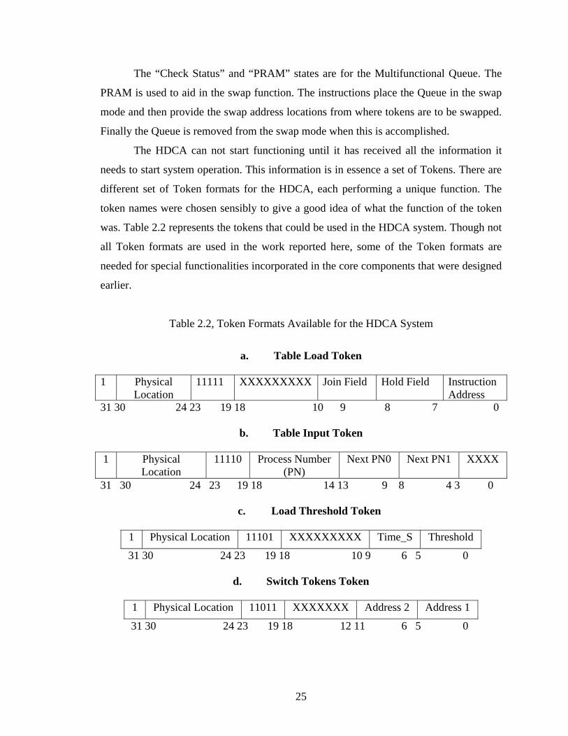
The “Check Status” and “PRAM” states are for the Multifunctional Queue. The
PRAM is used to aid in the swap function. The instructions place the Queue in the swap
mode and then provide the swap address locations from where tokens are to be swapped.
Finally the Queue is removed from the swap mode when this is accomplished.
The HDCA can not start functioning until it has received all the information it
needs to start system operation. This information is in essence a set of Tokens. There are
different set of Token formats for the HDCA, each performing a unique function. The
token names were chosen sensibly to give a good idea of what the function of the token
was. Table 2.2 represents the tokens that could be used in the HDCA system. Though not
all Token formats are used in the work reported here, some of the Token formats are
needed for special functionalities incorporated in the core components that were designed
earlier.
Table 2.2, Token Formats Available for the HDCA System
a. Table Load Token
1 Physical Location
11111 XXXXXXXXX Join Field Hold Field Instruction Address
31 30 24 23 19 18 10 9 8 7 0
b. Table Input Token
1 Physical Location
11110 Process Number (PN)
Next PN0 Next PN1 XXXX
31 30 24 23 19 18 14 13 9 8 4 3 0
c. Load Threshold Token
1 Physical Location 11101 XXXXXXXXX Time_S Threshold
31 30 24 23 19 18 10 9 6 5 0
d. Switch Tokens Token
1 Physical Location 11011 XXXXXXX Address 2 Address 1
31 30 24 23 19 18 12 11 6 5 0

26
e. Read Status Token
1 Physical Location 11100 XXXXXXXXXXXXXXXXXXX
31 30 24 23 19 18 0
f. Send Status Token 0 Physical
Location 0 Sign ITRC Threshold XXXXXXXXXXXXXXXXX
31 30 24 23 22 21 18 17 16 0
g. Load_PRT Mapper Token 1 PRT Location 11010 XXXX Physical
LocationProcess Number
RAM Address
31 30 24 23 19 18 15 14 8 7 3 2 0
h. Command Token
Hold Field Physical Location
Time Stamp
Process Number
XXXXXXXX Data Address
31 30 24 23 21 20 16 15 8 7 0
Out of these possible token formats, Token formats a, b, g and h were used for all
applications. The “Load Threshold” token was used in the application for demonstrating
dynamic node level reconfigurability. The tokens that are used to initialize the Look up
Table are the “Table Load” and “Table Input” tokens. These tokens, in essence, contain
information about the processes different CEs could possibly execute. They provide
information on the current process number, the following process numbers for the
successor nodes, the address of the process’s first instruction in local memory, a Hold and
a Join field. The remaining four tokens are used to access the advanced functionality of
the multifunctional queue if required. The “Load Threshold Token” identifies the queue
for a CE by the “physical location” of the CE and programs the threshold for the queue
and the time period (Time_s) desired for sampling the input and output rate. The “Switch
Tokens” token is utilized to swap tokens in the queue by address as previously mentioned
in this chapter. The “Read Status Token” and “Send Status Token” are designed to obtain
status information of a queue. The “Read Status Token” is sent by the operating system to
a CE directing it to provide status information. The “Send Status Token” is like an “ack”
containing the Input Token Rate Change (ITRC) over the specified time, its sign (positive
and negative) and a flag to indicate whether or not the threshold has been crossed for the

27
queue. “Load PRT” token is used to initialize the RAM in the PRT mapper upon system
startup. It contains information about the physical location (address) of the CE, the
process number that CE holds, and the RAM address within PRT to load this information.
This token is primarily responsible for starting application execution.
Each CE has a unique address which distinguishes it from the other CEs. Table
2.3 represents the physical addresses of the CEs as used in the current HDCA. These
addresses are essential for proper functionality of the token bus with the set of tokens
described above. The work done in [17] had 4 unique locations. However additional CEs
were added as part of the second phase modeling explained in the next chapter which
now leads to 6 unique locations.
Element Physical Location
PRT mapper 0000001
CE0(MR16) 0000011
CE1(MR16) 0000010
CE2(DIV) 0000100
CE3(MULT) 0000101
CE4(STANDBY) 0000110
Table 2.3, Physical Addresses of the Modules in the Prototype
Beside each CE, in parenthesis, is a brief description of its features. CEs 0, 1 and 4 are
the 16-bit unpipelined memory register computer architectures. CE2 and CE3 are the
special purpose multiplier and divider CEs. CE4 is a STANDBY CE (see Figure 2.8); it
is the CE that will be used to show the dynamic nature of the system by automatically
being configured and re-configured as needed when the queue depth increases beyond a
particular threshold as determined by the Operating System.

28
2.7 The Multiplier and the Divider CEs
The Multiplier and divider CEs are special purpose CEs. The Divider is a simple
core-generated pipelined divider. It uses unsigned arithmetic. Figure 2.12 shows the
divider CE used in the HDCA system.
Figure 2.12 : Divider CE. To be CE2 in the Latest Version HDCA
This processor is capable of receiving the data locations from the CE Controller and then
fetching its operands. The processor first loads one or two data location addresses into
registers (Data Loc 1 and Data Loc 2). Then, the start instruction is received from the CE
Controller. This provides it the first address in Instruction Memory to access. The first
Instruction provides an offset for the Data Locations if necessary. The system then
fetches the divisor and places it in a register (R1). If there is a valid address in the Data
Loc 2 Register, the divisor comes from the shared HDCA Data Memory; otherwise it is
29
loaded from the Instruction Memory. Next, the dividend is fetched from Data Memory
and placed in a register (R0). When both operands are loaded the division operation
begins. Twenty clock cycles later, the result is output and placed in output registers
(Result and Remainder). The results are then output to the shared HDCA Data Memory.
Lastly, the processor reverts to address zero and awaits the next process.
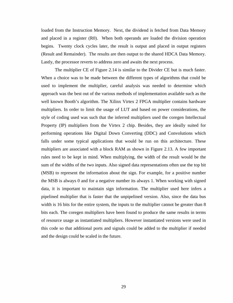
The multiplier CE of Figure 2.14 is similar to the Divider CE but is much faster.
When a choice was to be made between the different types of algorithms that could be
used to implement the multiplier, careful analysis was needed to determine which
approach was the best out of the various methods of implementation available such as the
well known Booth’s algorithm. The Xilinx Virtex 2 FPGA multiplier contains hardware
multipliers. In order to limit the usage of LUT and based on power considerations, the
style of coding used was such that the inferred multipliers used the coregen Intellectual
Property (IP) multipliers from the Virtex 2 chip. Besides, they are ideally suited for
performing operations like Digital Down Converting (DDC) and Convolutions which
falls under some typical applications that would be run on this architecture. These
multipliers are associated with a block RAM as shown in Figure 2.13. A few important
rules need to be kept in mind. When multiplying, the width of the result would be the
sum of the widths of the two inputs. Also signed data representations often use the top bit
(MSB) to represent the information about the sign. For example, for a positive number
the MSB is always 0 and for a negative number its always 1. When working with signed
data, it is important to maintain sign information. The multiplier used here infers a
pipelined multiplier that is faster that the unpipelined version. Also, since the data bus
width is 16 bits for the entire system, the inputs to the multiplier cannot be greater than 8
bits each. The coregen multipliers have been found to produce the same results in terms
of resource usage as instantiated multipliers. However instantiated versions were used in
this code so that additional ports and signals could be added to the multiplier if needed
and the design could be scaled in the future.

30
A performance of up to 200 MHz + can be inferred using this core multiplier as
mentioned in [34]. Figure 2.14 shows a block diagram of a typical multiplier CE in the
system. Since the multiplier is pipelined and the inferred multiplier is implemented on the
basis of Look up Tables in the chip, the result is obtained in one clock cycle. Using the
current design, the programmer is forced to utilize relative addressing for accessing data
items. Since the original data address provided by the Operating System is passed along
with each token, there is no way to use a different addressing scheme to access data
items. This certainly is a system limitation but works well for small systems.
Switch Matrix
Switch Matrix
Switch Matrix
Switch Matri
Block select RAM
8 x
8 M
ultip
lier
Figure 2.13: Core Multipliers associated with Block RAMs

31
Figure 2.14 : Multiplier CE used in the HDCA
All these components as described above, when put together along with the associated
I/O structure will form the latest version of the HDCA system addressed and will be
shown in the next chapter.
Pipelined Multiplier
Multiplicand Reg Multiplier Reg
Mux
Instruction Memory 8x16
Instr Mar
Mux
Data loc1 Data loc2
Mux Mux
Controller
R2
Mux
Mux
adder
16
8 8
8 8
16
8
8

32
Chapter Three Design Methodology and Modifications
3.1 Design Methodology
While designing the second and latest phase model of the HDCA, a "Top Down"
design system was utilized. In this approach, the problem is first defined and then split
into smaller manageable components. These smaller components are then developed,
tested and integrated into the main system. This approach allows the designer to develop
the components in a simple, modular fashion while maintaining focus on the system's
requirements.
3.1.1 Problem Definition
The first step in accomplishing the previously presented goals was to analyze the
background information and then define the problem statement. In this case, the initial
problem was to modify an initial version limited functionality prototype into a model that
could be behaviorally simulated. Next, the scope of the project was to design and
develop additional processors with their respective controllers, develop complex
applications for the system and demonstrate node level reconfigurability for the added
standby processors. Next, an additional feature was to be added wherein, the HDCA
could fork to more than two processes. An additional goal was to integrate the crossbar
Interconnect network switch developed in [32], into the system and the existing devices
re-configured to counter the latency introduced by the switch. The Operating System,
processor level re-configurability and replacing the addressing system would be left for a
future third phase model where an actual working hardware prototype would be built.

33
3.1.2 Requirements definition
Once these issues were identified, the next step was to identify system
requirements. It was known that before any work could be done on the second phase
model of the HDCA, a fully functional working first phase model was needed. This in
turn needed individual test benches to be developed for each component to test it for
deficiencies. Once success was achieved at getting a working model by making
modifications to the pre-existing components, the infrastructure had to be incorporated to
add the additional CEs into the system. This would require assigning new physical
locations to the CE and also maintaining the same system of communication that existed
between the other CEs. Another requirement was to develop Complex/Non-complex
applications that would utilize all the CEs and also bring out their dynamic,
reconfigurable nature. A more functionally desirable network switch was also integrated
into the HDCA system to make the design scalable, reduce bus contention and improve
system performance.
Next, the size of the system had to be determined. In order to fit the system on a
FPGA, it was decided to have a system with five CE's. Each CE would have a small
instruction memory and a connection via an interconnect network to a small shared Data
memory. Along with the decision on the number of CE's was the decision on how many
different types of CE's to use. It was decided that three different CE types would be
modeled in order to demonstrate the ability of the architecture to incorporate
heterogeneous systems. These CE's were chosen to be simple un-pipelined 16-bit
architectures and a special purpose pipelined divider and multiplier CEs in order to keep
the system complexity low and its area small.
Lastly, the total number of processes that the system could execute was bounded
to thirty-two or fewer with the exit PN being fifteen or lower. This helped to keep the
token widths to 32 bits and the experimental system to a more manageable size.
3.2 Design Flow Approach
There are many flowcharts that exist for design methodologies when using
Hardware Description Languages. Most of these begin with developing behavioral

34
models, testing those with pre-synthesis simulators, then altering the code in order to
synthesize the design. This approach has many benefits and is often necessary when
there are many limiting design factors such as signal timing. In this work there were no
such limitations or restrictions. Since this was an initial second phase model to
demonstrate the functionality of the architecture, there were no requirements to run at a
certain frequency or to fit in a particular device. Nor were there any standards which had
to be incorporated into the design in order to interact with another device. Given this
environment, it was decided to modify the approach taken. This decision coupled with
the natural flow of Xilinx's Foundation 6.2.3 ISE CAD software guided the design
process.
The overall design flow is shown in Figure 3.1.It was known early in the process
that the device would be synthesized and that it did not have to meet any particular timing
requirements. In terms of area, the only requirement was the goal of fitting the system on
a single Virtex 2 XC2V8000 chip. Second, the Foundation ISE 6.2.3i software allows for
pre-synthesis simulation, post synthesis and post implementation VHDL simulation
testing (post, place, and route).Of course, having to synthesize the code before running a
simulation wasted design time while it was running the synthesis tools, but this was
balanced by the fact that the developed code could be easily synthesized and
implemented as in contrast to the first phase prototype code that was started with. The
purpose of both pre and post simulation stages is to achieve functional validation of the
system. The post-implementation simulation validates that the system components would
function properly given the actual timing characteristics of the chosen target chip
resources and its routing delays. More detail about the testing is found in Chapter Six.
The Post place and Route phase (post-implementation) allows the user to input
system timing and placement constraints before mapping and placing the circuit on a
target FPGA chip. Again, constraints here were relatively few since there was no timing
or other requirements for the project. The HDCA prototype was synthesized, mapped,
placed, and routed to a Xilinx XC2V8000 FPGA chip with the 1152 package and a speed
grade of -5.

35
Figure 3.1 : Design Methodology for the HDCA System.

36
Next, the circuit can be tested again using post-implementation simulation. Here
the same test vectors were used, as before. Normally the idea here is to verify that the
circuit continues to meet the design goals now that the actual logic resource timing delays
are known. Post-implementation simulation is both a “functional” and a “performance”
simulation in that, the simulation includes the actual propogation delays of the logic
resources within the target FPGA chip. In this instance, it was important to verify that the
circuit still functioned properly, but there were no hard requirements which would
disqualify the circuit even if the actual timing was slower than predicted. As part of the
entire process mentioned above code is written, tested, corrected and then run through the
process again. This process can be time consuming and difficult. However, the process
can be made easier by breaking the problem into sub-components. If individual
components are tested from the beginning and taken through the entire design flow
process, the final system should in theory require less testing than a system designed as a
whole. Figure 3-2 illustrates the basic coding hierarchy utilized in this work. The overall
design was the PE chip and it consisted of four basic building blocks as shown. Each
sub-block consisted of lower-level modules and this hierarchy can also be seen in the
code when the project is set up.

37
Figure 3-2: Hierarchical Layout of VHDL Code for HDCA Prototype.

38
3.3 Modifications to the First Phase Prototype
In order to meet the HDCA system second phase prototype goals and
requirements, large scale improvements and changes were required to be made to the first
phase prototype system of [17]. Improvements and changes included modifying existing
functionality or adding new components. Also during the implementation phase it was
observed that Xilinx 5.2 ISE would frequently have software related issues Finally, a
design decision was made to move to the more stable Xilinx 6.2.3 ISE version of the
software which included a trade off between losses in development time versus a more
stable version of the code. In this section, functionality addition and other changes made
to the HDCA system to move it from the first phase prototype stage to a correctly
functioning second phase “virtual prototype” will be presented in a modular fashion.
Changes made to individual components will be discussed in detail.
3.3.1 PE Controller
The following issues were noted in the first phase prototype of the PE controller in [17].
The subtraction operation performed by the PE of Figure 2.8 was yielding incorrect
results. This was tracked down to the state OP5 of the PE Controller. Appropriate
changes were made in the code for this state to work. Also, additional changes were made
to include a new multiplexer M5 into the existing Memory Register Computer
Architecture of Fig 2.8. These changes allowed the output of the Instruction Register, IR0
to be directly sent to the Register R3. The changes that have been incorporated have been
shown separately in Figure 3.3 and also as a system in Figure 3.7.

39
Figure 3.3 : Changes to the PE Controller Showing the Additional Multiplexer M5
3.3.2 Interface Controller
The Control logic module of the Interface controller had to be modified for pipelined
execution of the applications that will run on the revised HDCA. In [17], the researchers
address the pipelined nature of the HDCA wherein, multiple copies of an application can
be run simultaneously on the system. The primary way to distinguish between different
copies of an application running on the system is by means of the “Time Stamp” field of
the command token shown in Table 2.2. As mentioned in [17], an application was
designed to test the pipelined nature of the system. However it was observed that the
system was displaying incorrect results. On a microscopic examination, it was attributed
to the signal “outbuf” in the control logic module. After execution of every process a
“Send PRT” and “StopL” token is issued to the PRT Mapper by the CE which completed
execution. The signal “outbuf” is used in the formation of the “Send PRT” token. As
multiple copies of an application are running simultaneously on the HDCA, it was seen
2x1 Mux M5
Register R3
M5out 8
Shifter
M5ctrl
IR0
1 0
To Mux before ALU
From ALU
From Instr Memory
8

40
that the value of “outbuf” for the first copy of the application was overwritten by the
second copy of the application causing loss of data for the first application. This
terminated the first application abruptly. For more details on the signal “outbuf” and the
formation of the “Send PRT” and “StopL” token, refer to the Appendix A of [35].
To fix this issue and get the HDCA to function properly with multiple copies of
an application, a provision was introduced to use the “Time Stamp” field of the command
token to differentiate between copies of an application. This involved introduction of an
array like structure to store the data required for the formation of these tokens. Also
changes were introduced in the command token format - bits 15 through 8, to distinguish
it from the other tokens circulating in the system. These bits are now set to logic one. As
part of this change, a new process “get_data” was integrated into the control logic module
to parse the command tokens properly. This new process can be seen in the code section
in Appendix A. Table 3.1 shows the new format for the Command Token.
Table 3.1, New Token Format for the Command Token of the HDCA
Command Token
Hold Field Physical
Location
Time Stamp Process
Number
11111111 Data
Address
31 30 24 23 21 20 16 15 8 7 0
Looking at this format, one can see that the “Time Stamp” is a three bit field allowing up
to eight command tokens to be issued, which are in essence, eight copies of an
application running in parallel.
One of the goals of the work reported here was to be able to show the queue depth
of the CEs build up and consequently, on reaching a pre-set threshold value, a new CE,
configured on the fly, to help out and reduce the load of the overloaded CE. This
capability of the HDCA is referred to as “Dynamic Node Level Re-Configurability”. It
was seen that when multiple command tokens were issued to the system, some tokens
were being lost and to fix this a new “Delay State” was added as shown in Figure 3.4.
This delay state, as the name suggests, introduced a delay of two clock cycles which
fixed the issue that was being seen.

41
Figure 3.4 : Control Logic for the Interface Controller Module
3.3.3 Crossbar Interconnect Network
The single-bus based logic used to access the shared data memory in the first
phase HDCA system was removed and a Crossbar Interconnect Network as developed
and described in [32] was integrated into the system. Since this introduced an additional
delay in the system due to the latency of the switch, changes were needed to ease this
transition into the HDCA. Figure 3.5 shows a block diagram of the interconnect network
that was used for the revised HDCA system. This allows multiple processors to access
the shared data memory at the same time. In the event that two processors with different
queue depths request access to the same memory block, the processor with the deepest
queue depth gets access to the block first while the other request is queued up. In the
event that the queue depths of both processors are the same, the processor with the
highest processor number gets access first while the other request is queued up. For a

42
detailed description of the Interconnect network functionality and the reasons for the
choice of a Crossbar Interconnect network, refer to [32].
Figure 3.5 : Crossbar Interconnect Network for the Revised HDCA
3.3.4 Input Rom for the Data
An input ROM was developed for the data to be input into the system. Core-
generated modules could not be used here because of the way the bus requests come in,
for data. Every third cycle there is a data request and to suit this functionality, an input
ROM was designed with a valid “signal” as output. The ROM would read out values, at
every clock cycle; however, only the values that are output every third cycle would be
valid and would be sent to the data bus. This ensured that correct values were read out
from the proper locations. Another approach to this could have been to use the core
generated ROM and use a “wrapper” around it. While this approach could have saved
considerable area, the design would not be scalable and would lose its ability of
“component re-use”.

43
3.3.5 Multiplier CE
This was another important addition to the system. While searching for
applications to be executed on this system, it was found that the existing operations were
insufficient for executing complex applications. Multiplication is an important operation
is the area of Digital Signal Processing and the architecture was limited in the sense that
there were no Computing Elements that could readily perform multiplication. Thus a
need for the Multiplication unit along with its associated controller was felt. This led to
the design of a new CE, the multiplier CE and its subsequent integration into the HDCA.
While making a decision about the algorithm to be chosen, a couple of options were
available. There were core multipliers in the Virtex 2 architecture on one hand and on the
other hand there were algorithms such as the Booth’s algorithm. While designing the
multiplier, it was kept in mind that this architecture would find use in embedded systems
or real time systems where area and power play important roles. A literature survey from
Xilinx revealed that using the core multipliers produced low power multipliers with fast
logic and used up less number of look up Tables. Additionally it would also consume
lesser power than a multiplier inferred using Booths or other such fast algorithms and
hence a design decision was made to use the style of coding as represented in the
Appendix. While, this directly does not use the core multipliers, the multipliers inferred
on synthesis of the code are core multipliers and hence all the important aspects
mentioned above apply to it.
3.3.6 Dynamic Load Balancing Circuit
While testing the basic functionality of the HDCA with a simple application,
(Application 1 of Chapter 6), and as shown in Figure 3.5 below, it was observed that the
join operation of processes P2 and P3 to yield process P4 was displaying incorrect
results. On careful analysis, the issue was traced to the Dynamic Load Balancing Circuit
module. As can be seen from Figure 3.6, during the join operation of P2 and P3, the
register R6 as shown in Figure 2.4, is used to store the values of the Physical Location,
Process Number and the Data Location.

44
Figure 3.6 : Simple Application 1 for the HDCA system
This is a special register in the sense that it stores the Process Number and Physical
location of the current process, say P2; to be used by the consecutive process, say P3; so
that they map to the same follow on process, P4. The values stored in R6, weren’t being
assigned properly to the consecutive process, resulting in the system failing to understand
that the processes are intended to join at the next process, P4 in this case. The logic added
has been documented in Appendix A.
3.3.7 Memory-Register Computer Architecture CEs
The Memory-Register Computer Architecture CEs (Figure 2.8) were also found
to need functional improvement. On delving through the code, a number of errors were
noticed. These errors did not cause issues in a behavioral simulation. However, while
going through post place and route simulation, the CE0 and CE1 modules stopped
functioning. Both these CEs use a number of registers which have asynchronous high
reset signals. These signals should clear the registers in system reset state. However the
“reset” pin of the registers was tied to logic zero all the time leading to errors in post
place and route simulation. Another problem lied in the fact that the bi-directional data
bus was a direct input to the multiplexer before the ALU. This caused unknown values to
enter the system that cascaded through the combinational logic in the system. This also
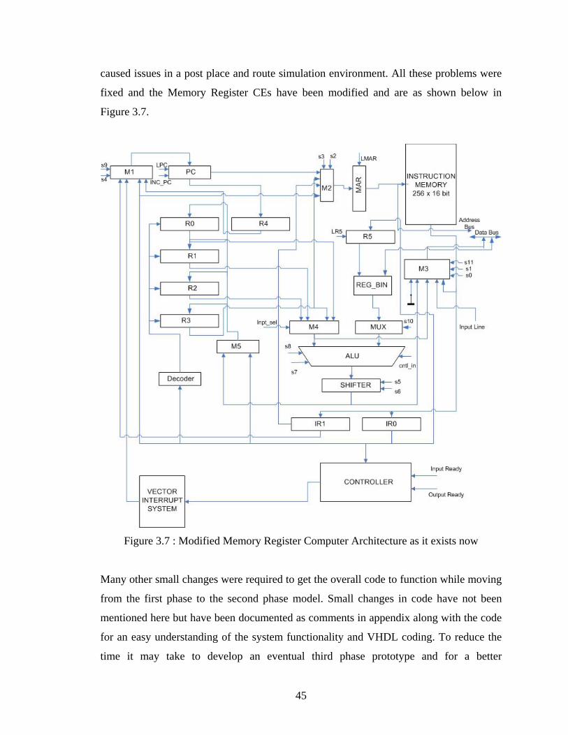
45
caused issues in a post place and route simulation environment. All these problems were
fixed and the Memory Register CEs have been modified and are as shown below in
Figure 3.7.
Figure 3.7 : Modified Memory Register Computer Architecture as it exists now
Many other small changes were required to get the overall code to function while moving
from the first phase to the second phase model. Small changes in code have not been
mentioned here but have been documented as comments in appendix along with the code
for an easy understanding of the system functionality and VHDL coding. To reduce the
time it may take to develop an eventual third phase prototype and for a better

46
understanding of the system, the VHDL code describing the HDCA (Appendix A) has
now been well documented.
3.4 Second Version (Phase) HDCA System
Functionality and other enhancements and fixes to the major functional units of
the first version (phase one) HDCA system has been described in previous sections of
this chapter. All these functoinal units were structured, interfaced and connected in a
manner resulting in a five CE second version (second phase) HDCA system as shown in
Figures 3.9. The enlarged view of the associated CE Controller along with its
components has been shown in Figure 3.8 below.
Figure 3.8 : An Enlarged Figure of the CE Controller Showing all its Functional Units

47
Figure 3.9 : Block Diagram of the Second Phase HDCA System

48
The CE Controller shown in Figure 3.8 was already described in the previous chapters.
The modifications to the Look Up Table, Fifo Queue and the Interface Controller have
also been described in Chapter 3. These three units, with their described changes, when
interfaced together form the CE controller for the Memory Register Computers, CE0,
CE1 and the Standby CE. The controllers for the Multiplier CE and Divider CE have
been shown as separate entities in Figure 3.9 to maintain uniformity. These are however
resident within the high level block of the Multiplier and the Divider CEs.
49
Chapter Four
Virtual Prototype Development
4.1 The Virtual Prototype
The HDCA system will be implemented to what is called the “Virtual Prototype”
level where-in a Post Place and Route HDL model of the HDCA with enhancements will
be developed and shown to work for two different applications. The bit-stream will not
be downloaded to a prototyping board. Instead, it will be left at a stage wherein as part of
future HDCA developments, the bit stream could be downloaded to a physical hardware
prototype.
The first application that will be taken through the Post Place and Route process is
the application with Multiple Forking (Figure 5.7) of Chapter 5. The second application
that will be demonstrated is the Fourth Application of Chapter 6, which is the Acyclic
Integer Manipulation Algorithm (Figure 4.40). A pipelined version of this will also be
shown to work behaviorally and to prove that a non-pipelined version would also run
fine, only one of the two command tokens will be used for the HDL Post Place and Route
Simulation.
4.2 The Simulation Environment and Overview of the Testing Process
Simulation testing of the HDCA was first carried out using the Xilinx 5.2ISE
CAD software. The simple application developed initially (Application 1 of Chapter 6)
passed the post-implementation simulation testing. Later, the HDCA system was
implemented and simulation tested using the Xilinx ISE 6.2.3 ISE CAD software [30].
Modelsim 5.7g PE version (31) is used as the simulator and the host PC was a high
performance AMD Athlon processor running Windows XP, 32 bit edition at 2.16 GHz
with 2GB of RAM. Input stimuli are added through the HDL bencher, where the timing
constraints could also be specified. After Synthesis, Implementation is done and as part
of this the Map, Place and Route algorithm is executed. Then, Post-Implementation
simulation is carried out using Modelsim with the test vector set provided in Appendix B
for different applications and after the Input ROM and the Instruction Memories have
been initialized using the Memory Editor tool provided in Xilinx. The simulation results
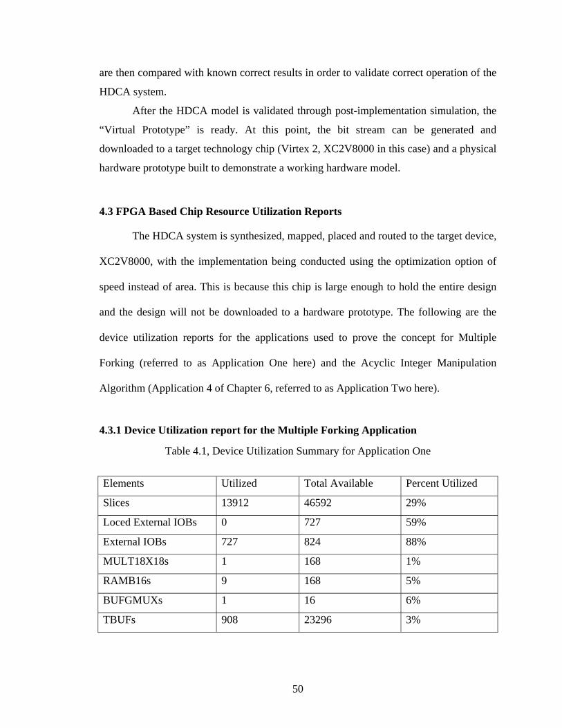
50
are then compared with known correct results in order to validate correct operation of the
HDCA system.
After the HDCA model is validated through post-implementation simulation, the
“Virtual Prototype” is ready. At this point, the bit stream can be generated and
downloaded to a target technology chip (Virtex 2, XC2V8000 in this case) and a physical
hardware prototype built to demonstrate a working hardware model.
4.3 FPGA Based Chip Resource Utilization Reports
The HDCA system is synthesized, mapped, placed and routed to the target device,
XC2V8000, with the implementation being conducted using the optimization option of
speed instead of area. This is because this chip is large enough to hold the entire design
and the design will not be downloaded to a hardware prototype. The following are the
device utilization reports for the applications used to prove the concept for Multiple
Forking (referred to as Application One here) and the Acyclic Integer Manipulation
Algorithm (Application 4 of Chapter 6, referred to as Application Two here).
4.3.1 Device Utilization report for the Multiple Forking Application
Table 4.1, Device Utilization Summary for Application One
Elements Utilized Total Available Percent Utilized
Slices 13912 46592 29%
Loced External IOBs 0 727 59%
External IOBs 727 824 88%
MULT18X18s 1 168 1%
RAMB16s 9 168 5%
BUFGMUXs 1 16 6%
TBUFs 908 23296 3%

51
Number of Gates 895077
4.3.2 The Delay and Timing Summary Report – Application One
The score for this design is: 529
The number of signals not completely routed for this design is: 0
The average connection delay for this design is: 2.172
The maximum pin delay is: 18.858
The average connection delay on the 10 worst nets is: 15.588
Timing Summary
Speed Grade: -5
Minimum period: 21.516ns (Maximum Frequency: 46.477MHz)
Minimum input arrival time before clock: 12.957ns
Maximum output required time after clock: 14.407ns
Maximum combinational path delay: 8.562ns
From the above report, it is evident that a lot of the External IOBs are utilized.
One of the reasons for this was the large number of signals that were taken out as ports
for debugging the system when it had issues. These ports were kept intact and hence the
device utilization report shows a high number for the External IOB usage. These ports
can be safely removed and this would help get down the number of IOB usage.
4.3.3 Device Utilization Report for Un-pipelined Integer Manipulation Algorithm
The device utilization report for Application Two is shown below. Again, only important
aspects of the report have been shown here. The number of External IOBs used is again
high, for the same reason.
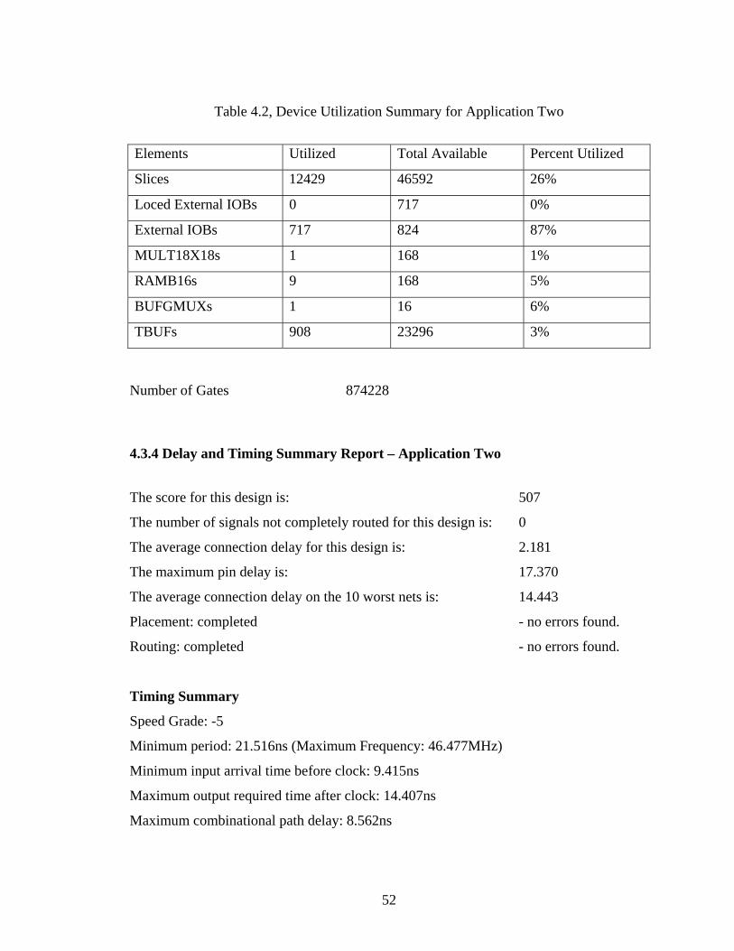
52
Table 4.2, Device Utilization Summary for Application Two
Elements Utilized Total Available Percent Utilized
Slices 12429 46592 26%
Loced External IOBs 0 717 0%
External IOBs 717 824 87%
MULT18X18s 1 168 1%
RAMB16s 9 168 5%
BUFGMUXs 1 16 6%
TBUFs 908 23296 3%
Number of Gates 874228
4.3.4 Delay and Timing Summary Report – Application Two
The score for this design is: 507
The number of signals not completely routed for this design is: 0
The average connection delay for this design is: 2.181
The maximum pin delay is: 17.370
The average connection delay on the 10 worst nets is: 14.443
Placement: completed - no errors found.
Routing: completed - no errors found.
Timing Summary
Speed Grade: -5
Minimum period: 21.516ns (Maximum Frequency: 46.477MHz)
Minimum input arrival time before clock: 9.415ns
Maximum output required time after clock: 14.407ns
Maximum combinational path delay: 8.562ns

53
4.4 Timing Constraints Definition for Post Implementation Simulation
After post-synthesis testing of the HDCA second phase model, the HDCA is post
implementation tested. The system clock is set with a period of 100 ns with a 50% duty
cycle as shown in Figure 4.1
Figure 4.1 : Timing constraints for Post Implementation Simulation
For the work described in [17], it was suggested that the minimum input setup time and
maximum output delay time be set to 0 ns to get rid of timing constraints error. As a first
step this was tried out. However, HDL bencher does not allow the constraints to be set to
0. These timing constraints were important to get rid of some Timing Violations that
were being observed for the system. On experimenting with different values, it was found
that the values of 10 ns for Maximum Output delay and 15 ns for Minimum Input Setup
time helped to address the issues.
Thus the HDCA “Virtual Prototype” system was developed to be robust and ready
for the Physical Prototype phase.

54
Chapter Five
Functional Enhancements to the HDCA
5.1 Dynamic Node Level Re-configurability
5.1.1 Introduction and Concept
In the work done in [13,14], the researchers refer to the additional ability of the
system architecture to dynamically configure/move or assign processors or other physical
resources to application processes which may unexpectedly become overloaded. The
researchers refer to this feature of the system as “Dynamic Node Level Re-
configurability”. One of the most important goals of the second phase model of the
HDCA was to make it dynamically node-level reconfigurable. Often in real and non-real
time systems, it is seen that the system load can unexpectedly increases beyond a certain
statistically calculated or predicted threshold. This may cause the system to get
overloaded and/or fail unexpectedly. A simple example of this may be a radar signal
processing system that tracks incoming aircrafts. An HDCA system maybe designed to
track a maximum of fifty aircrafts at any given time. If for some reason, seventy five
aircrafts arrive in the region simultaneously, the system should be able to dynamically
cope with this unexpected overload and exhibit correct functionality. This brings in the
concept of Dynamic Node Level Re-configurability wherein, a dormant node or a CE
could be configured and/or re-configured dynamically to handle the additional load on
the system and go back to stand-by mode once the system load has reduced to one within
normal operating conditions.

55
Figure 5.1a : Dynamic Node Level Re-configurability
Figure 5.1a illustrates the concept of Dynamic Node-level Reconfigurability. Assume
Static Resource Algorithm indicates one copy of Process P1 is required. Let the “one
copy” process running on a CE processor be represented by P11. Assume that
unexpectedly control tokens coming into the queue of the CE executing Process P11
increase in input rate to a point where they exceed the set threshold of the token queue.
This means Process P11 can not meet the process request rate and it needs help. In the
HDCA system dormant CEs can be initiated and programmed to implement process P11.
The process flow chart segment of Figure 5.1a indicates that two additional copies of
process P11 represented by the dotted circles P12 and P13, have been on the fly,
dynamically initiated and each is running on a different initially dormant CE. The HDCA
should have the ability to startup dormant processors in a system to help out overloaded
processors as determined by the control token queue depth.
5.1.2 Assignment Policy and Implementation
For implementing this important concept, the final loop application described in
Chapter 6 (Section 6.5) will be used. Please refer ahead for an explanation of this system.
This application was found to be complex enough to observe queuing in the system,
which is a pre-requisite for dynamic node level re-configurability. The increase in queue
depth indicates that the system is getting overloaded and is about to reach its normal
prescribed maximum load. Figure 5.1 shows the tokens being input shows two “load-
threshold” tokens that are inputs to the system through the HDL Bencher. Also, eight
command tokens are provided as inputs. These are in essence, eight copies of the looping

56
application being executed on the system. The data that these tokens operate on may be
the same or different but is irrelevant here considering the fact that a proof of concept of
this new feature is being provided. The eight command tokens cause pipelined execution
on the system and overload the system beyond its designed threshold causing the standby
CE or the dormant CE to kick in.

57
Figure 5.1 : Two Threshold Tokens and Eight Command Tokens being input into the System
8 command tokens or 8 copies of the application Avlsig0 and avlsig1

58
Another option that was possible was to get the standby CE to dynamically configure
itself, when both CE0 and CE1 got overloaded. The second choice was chosen while
arriving at a decision due to a number of reasons. Firstly, considering the nature of the
application under consideration, it was seen that there would have been a lot of switching
that could have occurred if the first option was used. This would essentially cause
reduced performance of the system if the standby CE would re-configure repeatedly and
then go back to dormant mode; more so, when implemented as a system on chip. Also,
since one CE in the system was still not overloaded, it was decided that the additional
load on the system should now go to this CE until it too gets overloaded and then the
stand-by CE would be configured. This makes perfect sense considering the fact that it
would reduce the repeated switching of the standby CE into and out of the system and
hence keep performance losses to a bare minimum. One may argue that since overloading
of a system is something that does not happen frequently, the performance losses due to
switching do not apply. This is the main reason that the nature of the application should
be first considered while making this important policy decision. Additionally, for making
the system flexible, the first option was still kept open. By making a small adjustment in
the “PRT Controller” logic of the system, which is a small change of an “and” gate to an
“or” gate, the first option could be implemented. This helps the designers make their own
choice before they design the code for application and configure the bit stream to be
downloaded into the FPGA.
Referring to the token formats described earlier, the “Load threshold” token has
its last field as the “Threshold field”. This is a programmable value which can vary
between 0 and thirty two. For the system under consideration, the value of the threshold
field was set to five. Additionally, it should be remembered that the queue depth and
threshold are two different values. The queue is deeper than the threshold. This is akin to
the concept in system design where a system is designed to “operate” under a particular
rating but at the same time some amount of “tolerance” is also provided. In the limiting
case, the queue depth can be equal to the threshold but under no circumstances can it be
lesser than the threshold. Referring to Figure 5.1, the signals “avlsig0”, “avlsig1” and
“avlsig5” are the queue depths of CE0, CE1 and CE5. The queue depths of the other CEs
have not been shown because they are not used in this application and lie dormant in the

59
system. The signal “prog_flag” indicates the threshold value for the system that we just
discussed about and as is evident from Figure 5.2, this gets set to a value of five for CE0
first and eventually for CE1 as well.
In Figure 5.2, it can be clearly seen that the thresholds have been set for the
system and the system has started execution. The first process, which is the input of the
numbers x”3C”, x”64”,x”0A”,x”3C” and x”64” at consecutive locations starting x”03”,
starts for most of the command tokens. The queue depth varies between zero and two.
Since the first process has not yet completed for a majority of the command tokens, it
hasn’t yet forked into two follow-on tokens each and hence the load on the system is
relatively low. Once the forking process completes for most of the command tokens, as
can be seen from the instructions of x”9C21”, x”9C28” etc. on the bus
“db_pe_icm_fin0”, “db_pe_icm_fin1” in Figure 5.3, most of the resulting tokens are
issued to CE1 causing its queue depth to rapidly increase to a value of five. Additionally,
as can be seen from the value on the signal “avlsig5”, even though the threshold flag has
been set for CE1, the stand-by CE has not yet dynamically kicked in, which verifies the
policy decision that was taken. Also, as can be seen, the other tokens are now sent to
CE0, indicated by value of the signal “avlsig0” at the cursor. This causes the queue depth
of CE0 to increase as well.

60
Figure 5.2 : Process 1 Executed for the 4 Command Tokens and “Prog_Flag” being set
Avlsig0 and avlsig1
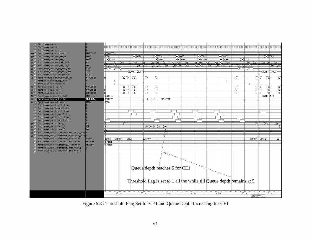
61
Figure 5.3 : Threshold Flag Set for CE1 and Queue Depth Increasing for CE1
Queue depth reaches 5 for CE1
Threshold flag is set to 1 all the while till Queue depth remains at 5

62
Figure 5.4 : Both Thresholds set and Standby CE Reconfiguring
Once both thresholds are set, the command token for the next instruction is given to the standby CE.
Avlsig0 and avlsig1

63
Once both thresholds are set, approximately at 68 us into the run as indicated in Figure
5.4 by the last 2 signals in the waveform, the next token x”0645FF0F” is now issued to
the standby CE. Also, its queue depth goes to a value of one as indicated by the signal
“avlsig5” and once it finishes executing the process it had started with, the depth goes
back to x”00” indicating that the standby CE has once again gone into stand-by mode
after doing its job. It is noteworthy to remember that had the tokens been issued to CE0
or CE1 instead of the standby CE, the next token would have been either
x”0345FF0F”(for CE0) or x”0245FF0F”(for CE1). This goes on a number of times into
the run.
For the sake of brevity, all instances have not been shown as that would require
tens of waveforms considering the run time for the application with eight command
tokens. What is important here is to remember that this application provides a proof of
concept of this feature and successfully implements this feature based on the policy
decisions. Another instance of the dynamic node level re-configurability has been
indicated in Figure 5.5 as shown below.

64
Figure 5.5 : Standby CE Kicking in to take in the Additional Load on the System
Once both thresholds are set, the command token for the next instruction is given to the standby CE.

65
At approximately 80.4 us, both CEs reach their threshold limit causing the standby CE to
take in the next token as is indicated by the value of x”0685FF1C”, which is actually the
process P5.
Thus, the concept of Dynamic Node Level Re-configurability is demonstrated and
incorporated into the second phase model of the HDCA. The tracers shown and the
results discussed verify the same.
5.2 Multiple Forking
5.2.1 Introduction and Concept
One of the restrictions of the first phase model of the HDCA was its restricted
ability to be able to fork to just two successor processes. As initially described, a process
flow graph can fork to two processes. The information about these two processes is
stored in the look up table through the “Table Input” token. Ideally, a process flow graph
may have any of the following topologies.
(a) (b) (c)
Figure 5.6 (a), (b) and (c) : Different Flow Graph Topologies
In real and non-real time systems, to extract the maximum amount of parallelism inherent
in an application and supported by the hardware, it is desirable to execute as many
processes as possible in parallel on different available processors causing the application
to execute in a shorter time. This is possible by the concept called as “Multiple forking”
where one process forks to multiple follow on processes which can then execute in
parallel on the different processors in the system.

66
5.2.2 Implementation
The first phase model of the HDCA could only fork to two processes as shown in
Figure 5.6 (a). A typical process flow graph, however may take a shape as shown in
Figure 5.6 (b), that is; it could fork to three or even four processes. To handle this feature
while maintaining the original architectural constraints, the approach shown in Figure 5.6
(c) was taken. Here, the first process forks into two processes, as shown in Figure 5.6 (c).
While the top process is a normal process, the bottom process is just a dummy process,
which again forks to produce two actual processes. The dummy process does not do any
actual useful work and it can be thought of as a “no-op” operation. It just serves as a
channel for allowing multiple forking to occur without any issues. The first process, thus,
in essence, forks into three actual processes. The same concept can be extended to four or
more processes by making the result of the first fork in Figure 5.6 (c) into two dummy
processes which then again fork to produce two actual processes each, thus effectively
forking to 4 processes. This concept was proved to work by implementing an application
all the way to post place and route validation. To implement this “no-op” operation, an
additional instruction was added to the Instruction set architecture of the Memory-
Register Computer architectures. The change involved adding an additional state to the
controller of the Processing Element. This was the addition of another state called the
“no-op” state which was a dummy state introducing a small delay. Since this process had
to be represented with its own set of “Table Load” and “Table Input” tokens, this
provided the two additional fields required for forking into three processes as described
in the tracers for the application shown below.

67
5.2.3 Post Place n Route Simulation Validation of an Application with Multiple Forking
Figure 5.7 : Application Flow Graph for Multiple Forking
Figure 5.7 shows a process flow graph for an application that provides a proof of concept
for multiple forking. In the following section, post place and route validation results
prove that the virtual prototype with this feature works fine and hence is able to
successfully fork into more than two processes through a dummy process, thus
overcoming the restrictions of the first phase model.
For the application shown above, one command token was used and its value was
set to x”01010003” as shown in Figure 5.8. Process P1, is the first process in the system.
As with most of the applications, this process provides the input data for the application.
In this case, the input data is a set of values x”02”. Figure 5.9 shows this value being
input into the system. These values are stored at consecutive locations in memory starting
from location x”03”.
Once this is over, process P2 starts executing adding the first two values of x”02”,
producing a result of x”04” eventually which is stored at location x”0A” in the shared
data memory and also a token for the third process P3 is issued as shown at the location

68
of the cursor by the highlighted value. This process is to be done by CE1 as it is found to
be and it also starts executing. This has been indicated in Figure 5.10.
Process P3 is a dummy process and it does not do any useful work in the
system other than introducing a delay. This can be seen from the instruction x“9C03
3000” in Figure 5.11. Also, it can be seen that process P2 completes and the
multiplication process starts execution as indicated by the instruction x”8E03 FF04”. The
dummy process forks into two actual processes P4 and P5 which do the addition
operations as can be seen in Figure 5.12, producing results of x”04” and x”04”, which are
stored at locations x”14” and x”1E” respectively in the shared data memory. Process P6
then executes. As part of the join operation, it subtracts values of x”04” from x”04”
producing a result of zero; which is stored at location x”2E”. This is shown in Figure
5.13.

69
Figure 5.8 : One Command Token of x”01010003” for the Multiple Fork Application

70
Figure 5.9 : Values of x”02” being Input into the System

71
Figure 5.10 : Token for P3 Issued and P2 Completes Execution

72
Figure 5.11 : The Dummy Process P3 and the Instruction for Multiplication
Delay Instruction
Instruction for Multiplication

73
Figure 5.12 : Process P4 and P5 Successfully Executing
P4 and P5- Adds two numbers to get a result of 4

74
Figure 5.13 : Join Operation - Subtraction is Performed Leading to x”0000” at x”2E”
Join Instruction
Final result
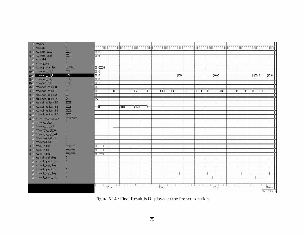
75
Figure 5.14 : Final Result is Displayed at the Proper Location

76
Thus multiple forking can be effectively achieved by using the concept of the dummy
process and this overcomes the architectural forking restriction of the first phase model of
the HDCA in [17].

77
Chapter Six
Example Applications Development, Testing and Evaluation for
Enhanced Fully Functional HDCA Process flow graphs can be classified under two broad categories, acyclic or cyclic
process flow graphs with single or multiple inputs/outputs. An acyclic process flow graph
has no feedback data going into processes that are earlier in the process flow. This
essentially means that there are no loops in the graph. A cyclic process flow graph, on the
other hand has feedback data dependence that form loops in the graph. Again, cyclic
process flow graphs could be split into deterministic or non-deterministic graphs. The one
with deterministic cycles of feedback loops, can be converted into an acyclic process
flow graph, if it is known early on as to how many loops are going to be executed. Thus,
it is not a true cyclic process flow graph. The one with non-deterministic cycles of
feedback loops, as shown in sixth application, is a true cyclic process flow graph. In this
chapter, six applications are described by the two types of process flow graphs mentioned
above. These applications go on to prove that virtually any application that can be
represented by a process flow graph can be execute on this architecture given that it
meets the restrictions imposed by the architecture definitions. Some applications
described are commonly used in image processing or other such areas in the field of
digital signal processing or embedded systems.
6.1 Application One: Acyclic Integer Averaging Algorithm
The first application represented here is a simple acyclic integer averaging
algorithm. This application was primarily developed to test the core functionality of the
different components in the system before additional processors were added in to the
system and after suitable changes were made to the code as provided in [35]. It can be
seen from this application that additional modifications, such as the input data ROM and
the multiplier processor have not yet been incorporated into the system keeping the
system simple but at the same time fully functional with the incorporated changes. Also it
can be seen from the images that the interconnect network has not yet been included in
the system.

78
Figure 6.1 shows a process flow graph for the integer averaging algorithm. The
process nomenclature and functionality can be described as below.
Figure 6.1 : Integer Averaging Algorithm
P1: Input ‘k’ numbers.
P2: Add first “k-2” numbers.
P3: Add remaining 2 numbers.
P4: Add the results of P2 and P3 to compute the sum of “k” numbers.
P5: Compute the average of the numbers by calculating “Result of P4”/k.
P6: Display the final results of the calculation.
In theory “k” could be a large number, for example, used when computing an average of
a large sample of data sets, as in the mean or median of the age of all the people living in
a county. However, to keep the first application simple and to provide a proof of concept,
a value of 6 was chosen for “k”. Any value of k > 2 would work for this system without
having the need to change the topology of the process flow graph.
As part of the first process “P1”, six numbers are inputs into the system via the
input bus “inpt_data0”. This can be seen in Figure 5.2 when “rq_ipt0” signal goes high
requesting input. In response to this request, the input data valid signal,”idv0” is made
high so that the value on the input bus is latched on .This can be seen in Figure 6.3 where
the first six numbers, all have a value of six and are stored at consecutive locations
P2
P3
P4
P6
P1
Input k numbers
Sum first (k-2)
Display Results
Add results of P2 and P3
Compute Average
Add remaining 2 numbers
P5

79
starting at 3, as represented by the “mem_ad_out” port. This is consistent with the values
shown in Appendix B. These processes have been indicated with an arrow and explained.
Process P1 forks in to two follow on processes P2 and P3 and next these are
executed. This can be seen in Figure 6.4, where the two processes are done by CE0 and
CE1 simultaneously. The instructions “300F” hex and “301A” hex refer to the locations
“0F” and “0A” hex where the instructions for these processes start. These locations have
been tabulated in Appendix B. As part of process P2, the first (k-2) numbers or four
numbers are summed. The result of the computation is stored at data location “0A”hex
and the result of P3 is stored at “09” hex. Also a high on the request output bus,
“rq_opt0” indicates that the system is requesting access to the bus to display the results
and when the grant is given, the results appear on the “mem_out” bus.

80
Figure 6.2 : Process P1 being done by CE0
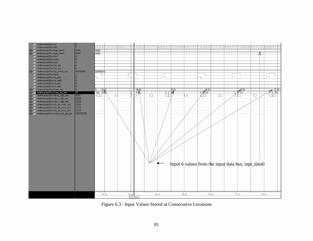
81
Figure 6.3 : Input Values Stored at Consecutive Locations
Input 6 values from the input data bus, inpt_data0

81
Process P1 forks to two follow on processes P2 and P3 and these are next executed. This
can be seen in Figure 6.4, where the two processes are done by CE0 and CE1
simultaneously. The instructions “300F” hex and “301A” hex refer to the locations “0F”
and “0A” hex where the instructions for these processes start. These locations have been
tabulated in Appendix B. As part of process P2, the first (k-2) numbers or four numbers
are summed. The result of the computation is stored at data location “0A”hex and the
result of P3 is stored at “09” hex. Also a high on the request output bus, “rq_opt0”
indicates that the system is requesting access to the bus to display the results and when
the grant is given, the results appear on the “mem_out” bus.
Once these processes finish execution, the next process P4 needs to execute. This
is a join process and operates on the two sets of data it receives from the locations where
processes P2 and P3 had stored their results. This is clear from Figure 6.5 where CE0
performs the join operation by collecting data from locations “09”hex and “0A” hex and
adding them to compute the final result, which is finally stored at location “0B” hex.
Once this is done, the last operation is the division operation. Division in the HDCA
system takes typically about twenty clock cycles. As part of the division process, value of
36 at location “0B” hex is taken by the divider CE and divided by the value of “k” which
is six and the final result of 6 is stored at the same location “0B” hex. This can be seen in
Figure 6.6. Finally, as part of the last process P6, the system displays the final result
computed. From Figure 6.7 it can be seen that the final value of the average of the k
numbers that were input in to the system is displayed.

82
Figure 6.4 : P2 and P3 being Done Simultaneously by CE0 and CE1

83
Figure 6.5 : Join Operation of P2 and P3 to P4 being done by CE0

84
Figure 6.6 : Average of the k Numbers being Computed by the Divider CE.
Result of 6 at location x”0B”
Division Operation going on

85
Figure 6.7 : Final Result of Algorithm being Displayed in Process P6 by CE0

86
The first application thus proved that the changes made to the existing first phase
prototype code to port it to the ISE platform were functionally correct and had no issues.
The next challenge was the inclusion of additional components and designing another
application that used these components along with the existing ones. This was
accomplished in the second acyclic application that was developed where an additional
multiplier CE was added along with an input data ROM. The second application is a two
by two matrix multiplication application with application in the area of Digital Signal
Processing.
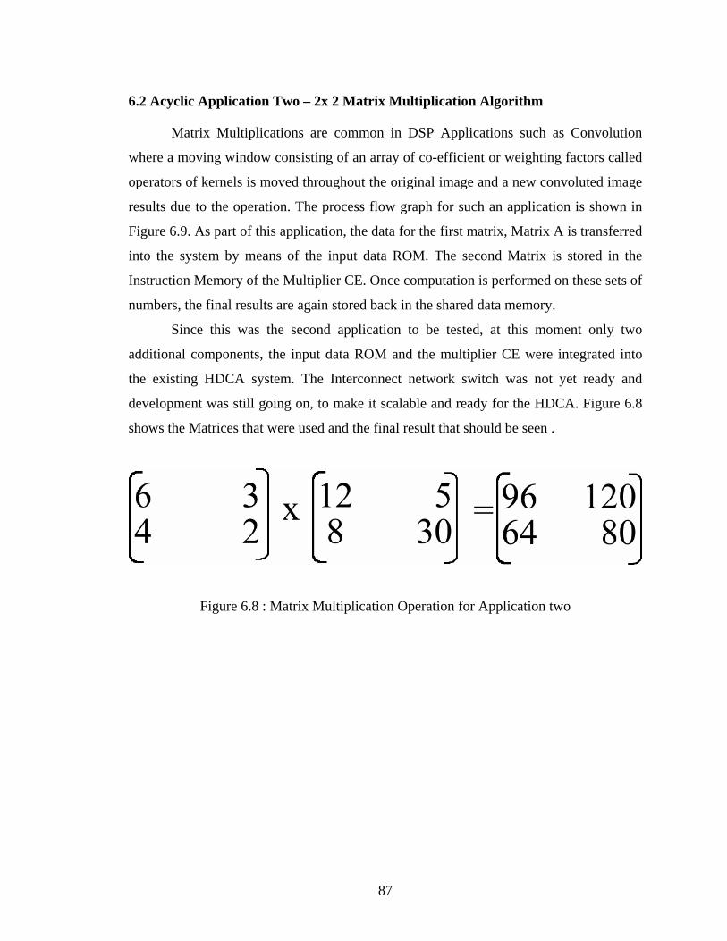
87
6.2 Acyclic Application Two – 2x 2 Matrix Multiplication Algorithm
Matrix Multiplications are common in DSP Applications such as Convolution
where a moving window consisting of an array of co-efficient or weighting factors called
operators of kernels is moved throughout the original image and a new convoluted image
results due to the operation. The process flow graph for such an application is shown in
Figure 6.9. As part of this application, the data for the first matrix, Matrix A is transferred
into the system by means of the input data ROM. The second Matrix is stored in the
Instruction Memory of the Multiplier CE. Once computation is performed on these sets of
numbers, the final results are again stored back in the shared data memory.
Since this was the second application to be tested, at this moment only two
additional components, the input data ROM and the multiplier CE were integrated into
the existing HDCA system. The Interconnect network switch was not yet ready and
development was still going on, to make it scalable and ready for the HDCA. Figure 6.8
shows the Matrices that were used and the final result that should be seen .
Figure 6.8 : Matrix Multiplication Operation for Application two

88
Figu
re 6
.9 :
2x2
Mat
rix M
ultip
licat
ion
Alg
orith
m fo
r App
licat
ion
2

89
For the entire representation below the notation Aij and Bkl is used, where i, k
represent the row numbers and j,l represent the column numbers. It is noteworthy to
remember here that for the two matrices A and B to be compatible for multiplication, the
number of columns of the first matrix should equal the number of rows for the second
matrix or in other words, j = k. Also, the resulting matrix would be of dimensions Cil.
P1: Input 2 sets of 4 numbers into the system.
P2: Multiply A11 and B11.
P3: Multiply A12 and B21.
P4: Compute C11= A11 x B11 + A12 x B21.
P5: Multiply A11 and B12.
P6: Multiply A12 and B22.
P7: Compute C12= A11 x B12 + A12 x B22.
P8: Multiply A21 and B11.
P9: Multiply A22 and B21.
P10: Compute C21= A21 x B11 + A22 x B21.
P11: Multiply A21 and B12.
P12: Multiply A22 and B22.
P13: Compute C22= A21 x B12 + A22 x B22.
P14: Display C11, C12, C21, C22.
Figure 6.10 shows two sets of the first four values of Matrix A being input into
the system from the input ROM. This is done by CE0 in response to the first instruction
that can be seen on the “db_pe_icm0_fin0” port. These values are stored at consecutive
locations starting from three, i.e from locations three to ten. The reason for storing two
sets of data is that when say for example, P2 finishes execution, it writes it’s result at the
same location where the original data was stored. In this case, originally a value of 6 is
stored at address 3 and when P2 gets over; the value at 3 gets updated to 72. However, we
require the old value of 6 again while performing computations for C12 and thus it needs
to be stored safely.

90
In some ways, this can be thought to be a limitation in the bus design, leading to
usage of additional resources in the HDCA. However, on the other hand, this is also
useful in recursive algorithms where the results of one operation need to be used by the
next process, as for example in finding the factorial of a given number which is often
used in Permutations and Combinations in the area of Mathematics.
The next process P2, multiplies a value of “6” at address “3” with a value of “12”
stored in the instruction memory of the muliplier to generate a result of “72” which is
stored back at location “3”. This can be clearly seen in Figure 6.11 where the ports of the
multiplier have been waved up as signals in the simulation for easy observation. As can
be seen from the code for the multiplier in Appendix A, whenever the newdata signal
goes high, dataa on the output of the multiplier is sent to the data bus for storage. The
same figure also shows the process P3 being done by CE0, where a value of “3” stored at
address “4” is multiplied by a value of “8” stored in the instruction memory of the
multiplier to yield a result of “24” which is stored back at location “4”.

91
Figure 6.10 : 2 sets of the First Four Values in Matrix A are Inputs into the System
Values being input from inROM
Command Token

92
Figure 6.11 : Process P2 and P3 being done by CE0 and their Results being Stored.
Process P2 Process P3

93
Once process P2 and P3 are done, the next operation to follow is the join operation where
the process P4, is used to compute the first phase of the final result, C11. This process
takes its data from the locations where processes P2 and P3 stored their final results and
computes the final result by doing an addition operation. This can be seen in Figure
6.12.Also it can be clearly seen that the data “72” is retrieved from location “3” and the
data “24” is retrieved from location “4” which corroborates the fact mentioned above for
the duplication of input data in the data ROM. The final result of the addition is “96”
which is stored at location “0B” hex in the data memory. This is also displayed as an
output when the request output signal goes high demanding access to the data bus to
display the output. Next, Processes P5 and P6 are executed and this can be seen in Figure
6.13- where a value of “6” is used, but this time retrieved from location “7” where it was
stored as a copy in the input ROM and multiplied with a value of “5” to yield a result of
“30” which is again stored at location “7”. Also as part of process P6, a value of “3”
from location “8” is multiplied with a value of “30” stored in the instruction memory to
yield a result of “90” which is again stored back at location “8”.
Next, as part of the join operation P7, these results obtained are added to compute
the final result of “120”. This is the C12 component of the final matrix and the value is
stored at location “0C” hex in the shared data memory. The result is also displayed on the
“mem_out” bus so that the data location and the value where the data is stored can be
easily cross-referenced with the values represented in the Appendix B. This has been
represented in Figure 6.14.
Similarly, processes P8, P9 do the multiplication and P10 does the join operation.

94
Figure 6.12 – Process P4 executed by CE0
Process P4 – A join operation
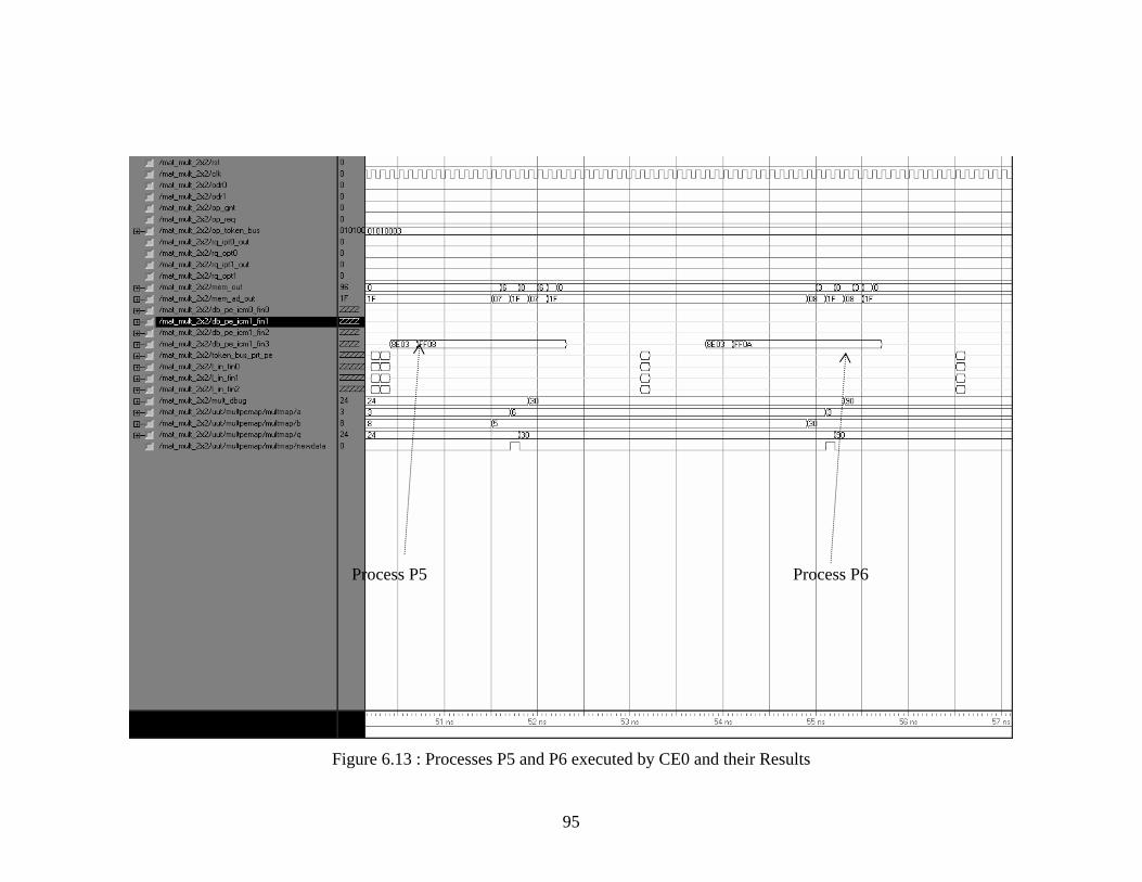
95
Figure 6.13 : Processes P5 and P6 executed by CE0 and their Results
Process P5 Process P6

96
Figure 6.14 – Process P7 being executed by CE0 and the Results Being Displayed
Process P7 – A join operation

97
Figure 6.15 : Processes P8 and P9 being Executed by CE0
Process P8 Process P9

98
Figure 6.16 : Process P10 being Done by CE0. It Computes Component C21
Process P10 – A join operation

99
The results obtained are added to get the C21 component of the final matrix. This
result is stored at location “0D” hex. These operations and the results can be seen in
Figures 6.15 and 6.16 respectively.
Once this has been done, the last section of the computation remains, where the
processes P11 and P12 first multiply the values “4” by “5” and “2” by “30” as shown in
Figure 6.17 and then the result of this operation is retrieved by the join process P13
which calculates the final component C22 of the resultant matrix and stores it at location
“0E” hex. This is displayed in Figure 6.18. Finally the last process P14, displays all the
results computed and stored so far or in other words it displays the contents of the shared
data memory where the results were earlier stored by the join processes P4, P7, P10 and
P13. These are the four final results of the matrix multiplication operation and can be
clearly seen in Figure 6.19. The final results of this algorithm are “96” located at location
“0B” hex.”120” located at “0C”hex. A value of “64” located at “0D” hex and a value of
“80” located at “0E” hex. These results are consistent with the 2x2 matrix multiplication
application for the matrices that were inputs into the system.
This application goes on to prove the diverse nature of the system. While it
accomplished the goal of successfully testing the newly designed components in the
HDCA, it also brought out the face that algorithms which find use in embedded
computing and DSP applications can be executed on this architecture. In fact the parallel
nature of the HDCA favors the operation of such algorithms. An important question that
arises is that of scalability and performance. It’s nice to know the increase in gate count
as application get bigger and the resulting changes in performance.

100
Figure 6.17 : Processes P11 and P12 done by CE0
Process P11 Process P12

101
Figure 6.18 : Process P13 Computing the Last Component C22
Process P13 – A join operation

102
Figure 6.19 : All Results with their Data Locations in the Shared Data Memory
96 at x”0B” 120 at x”0C”
64 at x”0D”
80 at x”0E” Final Process to display all results

103
To prove that the HDCA was scalable and that different types of matrix
multiplication algorithms could be run on it, an asymmetric matrix multiplication
algorithm was executed. Since the process flow graph of any application that can be run
on this architecture is limited to 32 processes, a 3x3 matrix multiplication operation could
not be run as it exceeded the process limit. Also, it would not help prove the fact that
asymmetric multiplications could also be done and hence, as part of application 3 that
was developed, a 3x3 matrix A was multiplied with a 3x2 matrix B to yield a final 3x2
matrix C.

104
6.3 Acyclic Application 3 – 3x3 by 3x2 matrix multiplication algorithm with
performance evaluation and gate count comparisons
Since the base algorithm that was used is the same as that of application 2 with a
difference only in dimensions, this application is not explained in as detail as application
two. Figure 6.21 shows a process flow graph for this application. The noticeable
difference in this graph compared to that of application two is an increased number of
processes, almost double those of application two, bringing this application close to the
maximum process limit and increasing its complexity. Also worth mentioning, is the fact
that each partial result computation, now has an additional multiplication operation
associated with it, leading to an increase in the amount of duplication. Thus the amount
of data in the input ROM can be represented by the equation O(data dup) = 2 * k2 for an
Figure 6.20 : Number of Elements in the Data Rom vs. Dimensions of Input matrix
input square matrix of dimensions ‘k’. Thus if there was a “3x3” matrix, the data ROM
would have 18 elements and so on. This is plotted in the Figure 6.20. From the plot, it is
clear that the rise in number of elements is roughly exponential with the increase in size
Number of Elements Vs Dimension
0
50
100
150
200
250
1 2 3 4 5 6 7 8 9
Dimensions of the Matrix
Num
ber o
f Ele
men
ts

105
of the matrix, which means that for very large matrices, the system would consume lot of
resources in the FPGA chip and subsequently would not fit in a single chip. Since the
HDCA system described here, was limited to thirty two processes , the need for fixing the
bus logic wasn’t felt necessary. The processes of this application can be described as
below.
P1: Input 2 sets of 9 numbers into the system. This is the first matrix- Matrix A.
P2: Multiply A11 and B11.
P3: Multiply A12 and B21.
P4: Multiply A13 and B31.
P5: Compute C11= A11 x B11 + A12 x B21 + A13 x B31
P6: Multiply A11 and B12.
P7: Multiply A12 and B22.
P8: Multiply A13 and B32.
P9: Compute C12= A11 x B12 + A12 x B22 + A13 x B32
P10: Multiply A21 and B12.
P11: Multiply A22 and B21.
P12: Multiply A23 and B31.
P13: Compute C21= A21 x B11 + A22 x B21 + A23 x B31.
P14: Multiply A21 and B12.
P15: Multiply A22 and B22.
P16: Multiply A23 and B32.
P17: Compute C22= A21 x B12 + A22 x B22 + A23 x B32
P18: Multiply A31 and B11.
P19: Multiply A32 and B21.
P20: Multiply A33 and B31.
P21: Compute C31= A31 x B11 + A32 x B21 + A33 x B31
P22: Multiply A31 and B12.
P23: Multiply A32 and B22.
P24: Multiply A33 and B32.

106
P25: Compute C32= A31 x B12 + A32 x B22 + A33 x B32.
P26: Display C11, C12, C21, C22, C31,C32
Since there are 26 processes that are to be executed and there are eighteen multiplications
to be performed, the size of the look up table needs to be increased for accomodating this.
Hence the look up table needed to have eighteen entries before it had all the data it
needed for the application to execute. Also its visible that there are twelve addition
processes that could be executed by CE0 or CE1 but this is less than the value of eighteen
needed to fill up the lookup table and hence six more sets of table load and table input
tokens need to be added. These can be any table load/ table input pair from earlier
processes. Figure 6.21 explains in great detail as to what each process does and the sets of
data it operates on. Also indicated by the side is information on the CE that performs the
given process.

107
Figure 6.21 : Process Flow Graph for Asymmetric Matrix Multiplication of Application 3

108
Similar to application two, one matrix is stored in the Instruction Memory of the
multiplier while the other values are input through the data ROM into the system. The
test vectors, Instruction Memory Initialization and other details of this application can be
found in Appendix B, which has test vectors for all applications discussed here. In this
section, only waveforms representing system operation have been shown. The system
begins operation at process P1, where two sets of Input data representing the first matrix
and input into the system. This can be seen clearly in Figure 6.22 through Figure 6.25.
The values are stored at consecutive locations starting from 3 and incrementing by 1. So
the first 9 values are stored at locations “03”hex through “0B”hex respectively. This can
be clearly seen in Figure 6.23 which shows the first set of last 4 values which end at “0B”
which has a value of “09”. Figure 6.24 clearly shows the data being repeated again
starting at location “0C” hex and ending at “14” hex as shown in Figure 6.25.
This represents the completion of process P1. Once the process P1 gets over the
next process to be executed are P2 and P3. In the figures that follow, a brief explanation
of each operation is given along with the figure. Details of system operation have already
been explained in Application two and will not be repeated again here. Processes P2,P3
and P4 are all multiplication processes that calculate part of the product needed to
compute the final sum of products. Figure 6.26 shows all three processes being executed
along with the results. The “mult-dbug” port has the final result which gets latched on to
the data bus and stored at the proper location as indicated in the waveform. This
completes all the information needed to compute the first SOP (Sum of Products).

109
Figure 6.22 : First 5 Values of the Matrix A being Input Through the Data ROM
Values 1,2,3,4 and 5 starting at consecutive locations from 3

110
Figure 6.23 : Last Four Values of the First Set of Data Stored at Locations Ending at “09”hex

111
Figure 6.24 – Second set of Data for Matrix A, Starting at “OC” hex

112
Figure 6.25 : Last 4 Data Values for Second Set of Matrix A, Ending at “14” hex
Address location 14 hex

113
Figure 6.26 : P2, P3 and P4 with Results, “16”, “2” and “12” Unsigned on “mult_dbug”
P2 P3 P4

114
Figure 6.27: P5 Being Done to Calculate C11.
Join Operation for P5
C11 calculated

115
Similarly Figures 6.28 through 6.29 show P6,P7 and P8 being done which are
multiplication operations storing data “12’, “4” and “18” at locations “0C”hex,”0D”hex
and “0E” hex respectively. Once this is computed, next the components C21 and C22 need
to be computed. These are computed by Processes P10 through P17 as shown in Figure
6.30 – Figure 6.33. Similarly the components C31 and C32 are likewise calculated by
processes P18 through P25 as is seen in Figures 6.34 to 6.37. Once all the results of the
matrix multiplication algorithm are ready, they are displayed once again, together to
verify the final result. It is lucid from Figure 6.38 that the correct values have been
computed and stored at the locations as described in Appendix B. These are namely,
unsigned values of 30,34,93,94,156 and 154 stored at hex locations 60, 61, 62, 63, 64 and
65 respectively.

116
Figure 6.28 : Processes P6, P7 and P8 being executed by CE 0
P6 P7 P8

117
Figure 6.29 : P9 Computes Sum of Products C12 stored at “61”hex in Data Memory
P9 computes sum
Result at x”61”

118
Figure 6.30 : Process P10, P11 and P12 – Multiplications being Done

119
Figure 6.31 –Process P13 Computes C21 Stored at “62”hex finally in Shared Data Memory
Instruction for P13 - Join
Sum stored at x”62”

120
Figure 6.32 – Processes P14, P15 and P16 Computing Products

121
Figure 6.33 : Process P17 Calculates C22 Stored at “63”hex Finally in Shared Data Memory
Unsigned 94 stored at x”63” in data memory

122
Figure 6.34 : Processes P18, P19 and P20 are Done by the Multiplier CE 4.

123
Figure 6.35 : Join Operation0Ccomputes C31 Storing it at “64”hex in Shared Data Memory
C31 computed- 156 at x”64”

124
Figure 6.36 : P22, P23 and P24 being Performed by CE4

125
Figure 6.37 : Last Component of Result being Calculated and Stored as part of P25
C31 computed- 154 at x”65”

126
Figure 6.38 : Final Results Being Displayed by Process P26
30,34,93,94,156,154 at x”60”,x”61”,x”62”,x”63”,x”64”,x”65”

127
Thus this algorithm goes on to prove the very important fact that matrices of any
dimension can be multiplied using this architecture if the restrictions of limitation to 32
processes are avoided besides, when the simple processors used are replaced by hybrid
processors, which can perform all kinds of operations, the inherent parallelism in these
operations can be made use of and better performance achieved.
Finally the results of both these operations were compared and a graph showing
performance with different speed grades has been shown in Figure 6.39. This gives a
good idea of system performance with increase in matrix size.
1
2
2 x 2 Mat Mult
3 x 2 Mat Mult
29
30
31
32
33
34
35
36
37
Frequency (MHz)
Speed Grades2 x 2 Mat Mult
3 x 2 Mat Mult
Figure 6.39 : Plot of Maximum Frequency vs. Speed Grades for Applications 2 and 3
The above figure shows the maximum frequency at which the HDCA could be run when
the multiplication algorithms were performed. It is clear that there is a vast improvement
in performance when moving from a speed grade of -4 (shown as 1 in graph) to a speed
grade of -5 (shown as 2 in graph). Also, it is evident that there is a slight improvement in
performance as the matrix size increases from that of application one to application two.
128
The next application described is pretty different in that it uses all the processors
in the system, unlike some of the applications that have been described just now and
introduces the concept of “multiple command tokens” hinted at in chapter 2.This is
explained in the next application along with the results obtained on running the
application. Gradually this concept is extended to demonstrate a complex loop
application and the dynamic node level reconfigurability concept.

129
6.4 Application Four – Acyclic Pipelined integer manipulation algorithm
Figure 6.40 : Process Flow Graph for Application Four
The process flow graph for this application can be split into the following processes –
P1 – Input “n” numbers into the Shared Data Memory from the Input Data ROM..
P2 - Add the first half of these numbers and store the result in the Shared Data Memory.
P3 – Add the remaining numbers in parallel and store the results in the shared data
memory.
P4 – Multiply the result of P2 by value “k” stored in the instruction memory of the
Multiplier CE.
P5 – Divide the result of P3 by value “k” stored in the instruction memory of the Divider
CE.
P6 – Subtract the result of P5 from P4 and store the result in the data memory.
P7 – Display the address and value of the final result calculated in P6.
At first glance this application looks like any other application previously
developed. However there are a couple of major change here. In all the applications that
had been described earlier, there was just a single copy of the application running on the
entire system. Moreover, a core generated shared data memory was used in the system.

130
Thus when multiple CEs requested for the bus, one or more CEs had to wait for the
access until the CE that was accessing memory was done with its work. This limitation
was removed in this application by the introdcution of the interconnect network switch in
the system as mentioned in [19]. In Chapter 2, it was mentioned that the HDCA could
support pipelined computation. This means that at any given time, there could be multiple
copies of a process flow graph running on the system. The copies running on the system
may or maynot operate on the same data values. This application shows the pipelined
nature of the HDCA by executing two copies of the above process flow graph in unison
thereby making the algorithm compute intense.
In order to accomplish this, two copies of command tokens are provided as test
vectors at the end of the test vector input phase. Each of these command tokens; as can be
seen from Table 2.2 in Section 2.6 of chapter 2, has a three bit field called “Time Stamp”.
This field helps the HDCA distinguish between different copies of a given application.
This is essential for proper operation of the HDCA. If there were no way to separate the
two copies and if we assume that the two copies of the application operate on different
sets of data, then the HDCA could, for example, erroneously perform some process, say
P6, by taking first value from copy 1 of the application and the second from copy2 of the
application. Since the “Time Stamp” field for both command tokens is different, this does
not happen. For the first command token, the “Time Stamp” field is set to logic zeros and
for the second command token it is set to a logic one. Also, worth mentioning is the fact
that the “Time Stamp” field is a three bit field, which means that at any given time, at the
most, eight copies of an application could be initiated on the system. In the application
described here, 10 values were input into the shared data memory through the Input ROM
and the value of k was chosen to be “2”. The initialization tokens and the command
tokens have been shown in Appendix B. The two command tokens, x“0101FF03” with
time stamp as “000” and x“0121FF11” with time stamp as “001”instruct the PRT mapper
to map the first process P1 for both the copies. The PRT mapper allocates CE0 for both
the copies of process P1, as CE0 has a higher priority over CE1 on process P1 and both
CEs are idle before the first process begins. Figure 6.41 shows the two command tokens
being issued to the CE0. The first instruction issued by the interface controller of each CE
is shown in the waveforms at the ports “db_pe_icm0_fin0” for CE0 and similarly for

131
other CEs. These output ports have been named based on their connections. Hence, the
said port is the bus between the CE and its interface controller module. CE0 begins
execution of process P1, and 10 values are transferred to the shared data memory through
the ‘inpt_data0’ bus. Figure 6.42 shows the first 5 values (all 2s in this case) being sent
into the data locations starting from x”03”of the shared memory block. The figure also
indicates CEs accessing, a particular block in the shared data memory, for instance in this
case CE0 is accessing block ‘blk0’. The remaining 5 values are similarly sent to the
shared data memory and this is indicated in the next figure, Figure 6.43. The values
stored in memory can be viewed at the “mem_out_0” bus.
According to the flow graph topology, P1 forks to two processes, resulting
in two command tokens (x“01020003” and x“01030003”) which are issued to the PRT
mapper to be allocated to the most available CE. This is depicted in Figure 6.44. The
PRT Mapper chooses CE0 as most available for process P2 and CE1 for process P3.
Again this is a feature that is decided by the Load PRT token. Figure 6.45 shows the
command tokens being issued CE0 for process P2 (x“0302FF03”) and CE1 for process
P3 (x“0203FF03”). When the first process for the first copy of the application finishes
execution, the execution of the second copy of the first process, P1 starts. This can be
seen in the instruction (“9C11 3003”). In the meantime CE1 starts execution of the
process P3 for the first copy (“9C03 3024”) of the application. In this case, both CE0 and
CE1 are accessing the same memory block ‘blk0’, however not at the same time hence
there is no simultaneous access. These events are depicted in Figure 6.46. Also the block
boundaries for shared data memory are defined in Appendix B.

132
Figure 6.41 : Command Tokens for both Copies of Process P1 to CE0 Issued by PRT Mapper
2nd Command Token 1st Command Token

133
Figure 6.42 : P1 – First 5 Values of Copy1 being sent to Shared Data Memory
Input 5 values as shown by arrows. All have a value of x”02”

134
Figure 6.43 - Input of Last 5 Values for Process P1 of Copy 1

135
Figure 6.44 : Two Command Tokens being Issued to PRT Mapper for Copy 1
Process P2 is the next
Process P3 is the next
Implies a fork

136
Figure 6.45 : Command Tokens Issued to CE0 and CE1 by PRT Mapper for Copy1
To CE0 by PRT Mapper To CE1 by PRT

137
Figure 6.46 : Instructions for Process P1 of Copy 2 and for Process P3 of Copy 1

138
The second copy of the application also follows the same flow graph, hence when
process P1 gets over and the CE indicates that it is finished with the current instruction,
two command tokens are generated by CE0 and issued to the PRT mapper, similar to
copy1. Figure 6.47 depicts this. The PRT again has to choose the most available CE.
Figure 6.48 shows that the PRT Mapper allocates P2 to CE0 and P3 to CE1 for the
second copy of the application, which is indicated by the tokens x“0323FF11” and
x“0223FF11”. Its handy to remember that CE0 has an address of x”03” and CE1 has an
address of “02” and hence a quick look at the command token always indicates which CE
is being allocated a given process. The execution of process P2 of copy 1 begins after the
end of process P1 of copy 2. The instruction x“9C03 3017” is being issued to the CE0.
This is shown in figure 6.49. In figure 6.50 it can be seen that the instruction for process
P3 is issued by CE1 x“9C11 3024” and also a command token x“01050003” for the
process P5 is being issued to the PRT Mapper as the execution of process P3 ends. The
process P5 is a division operation as shown in figure 6.51, it takes about twenty clock
cycles. The PRT Mapper allocates process P5 to the Divider CE as can be seen from the
token x“0405FF03”. All the results of computation are stored in the shared data memory
and these values can be referred to in Appendix B. The division operation is shown in the
figure 6.50, the division of value unsigned‘10’ (result of addition of last 5 values of
process P3) at x”0E”by unsigned’2’, the result unsigned‘5’ is obtained after a 20 clock
cycle delay and is stored at the same location of ‘10’ that is x”0E”. To exhibit perfect
division operation the ports of the divider CE are taken out and shown. At the end of the
execution the Divider CE sends the command token to the PRT Mapper x”81060003”

139
Figure 6.47 : Two Command Tokens Issued to PRT Mapper for Copy 2

140
Figure 6.48 : Two Command Tokens Issued to CEs by PRT Mapper for Copy 2 - P2 and P3

141
Figure 6.49 : Process P3 for Copy2 of the Application
Process P3 for Copy2 – Note the 9C11 indicating that it’s the second copy

142
Figure 6.50 : Division Operation in the Process of Execution.
Division

143
which implies a join operation to follow. The PRT Mapper will wait for the P4 process to
execute and issue similar token to the PRT Mapper. After the execution of process P2 by
CE0 it sends the command token x”01040003” to the PRT Mapper. The next process is
P4, a multiplication operation; hence the PRT Mapper allocates the process to the
Multiplier CE (CE4). It issues a command token x”0504FF03” to CE4. This is shown in
Figure 6.52. The figure also shows the issue of instruction for process P3 for copy 2 to
CE0 on the “db_pe_icm_0_fin0” bus.

144
Figure 6.51 : Division Operation for Process P5 with Results and Issue of Command Token to PRT Mapper for Copy 1
DivisionIssue of Command Token

145
Figure 6.52 : Command Token for Process P4 Issued to PRT Mapper and from PRT to CE4 for Copy 1
Command Token to PRT PRT to CE4

146
Figure 6.53 shows the multiplication operation after the issue of the multiply instruction
to the multiplier CE. An unsigned value of ‘10’ stored at location x”0D” (addition of first
5 values as part of process P2) is multiplied by ‘2’. The result, 20 is stored at same
location x”0D”. These values can be seen at port “mem_out_3” and location
“mem_ad_out_3” of the waveform. The ports of the multiplier CE have been added and
shown to display the functioning of the multiplier CE. At the end of process P4 a
command token is being issued by CE4 to the PRT Mapper x”81060003” which indicates
a join process P6 is next.
The process P2 of copy 2 after execution sends a command token for process P5 to PRT
Mapper and eventually the PRT Mapper sends the command token to the Divider CE.
This is shown in Figure 6.54. The detailed division operation is shown in figure 6.55.
Here the unsigned value ‘10’ stored at x”1C” is divided by the unsigned value of ‘2’. The
result, “5” is stored in the same location x”1C” as shown in the waveform of Figure 6.55.
Result is observed at “mem_out_2” and address at location “mem_ad_out_2”. Similar to
the division operation of copy 1 the divider ports have been waved up for display. The
following command token for process P6 is issued by CE2 to PRT mapper.

147
Figure 6.53 : Multiplication Operation by CE4 and Command Token Issued to PRT Mapper for Copy 1

148
Fig: 6.54 : Command Token for P5 Issued to PRT mapper and from PRT to CE2 for Copy 1
Division PRT to CE2

149
Figure 6.55 : Process P5 and Command Token to PRT Mapper for Copy 2
Process P5
PRT Mapper to Copy2

150
In Figures 6.53 and 6.55 it can be seen that two CEs are accessing the same
memory block ‘blk0’.Meanwhile the PRT Mapper allocates CE1 to compute the process
P6 of copy 1 as can be seen from figure 6.56. The instruction x”9C03 9803 3032”for the
join operation is issued to CE1. In process P6 the values obtained from the result of
process P4 are subtracted from result of process P5. An unsigned value of ‘5’ (result of
division) at location x”0D”, is subtracted from the result of multiplication, ‘20’ stored at
x”0E” and the final result of ‘15’ is stored at location x”0F”. The result of the process P6
is finally displayed by another process P7. The instruction for process P7 is executed by
CE0 x”9C03 3039”. This process outputs the results of the subtraction operation in P6.
Hence the result can be seen as explained earlier in figure 6.57. Also the command token
for process P4 of copy 2 being issued to PRT Mapper and eventually a command token
x”0524FF11” is issued to the Multiplier CE to execute the process P4 for copy 2 of the
application.

151
Figure 6.56 : Join Instruction for Process P6 of Copy 1
Join Instruction for P6

152
Figure 6.57: Instruction for P7 and Final Results for Copy1 of Application Displayed
Final Result at x”0F”

153
After the command token for the process P4 is issued to Multiplier CE, the
instruction is issued and multiplication takes place. The final result of the multiplication
is stored at the location x”1B”, where the earlier result of addition process was stored.
Once P4 is done, the command token x”81060011” for the join process P6 is issued. This
is shown in Figure 6.58
The PRT Mapper allocates the next process P6 to CE1 finding it to be the most
available. The instruction for the process P6 is issued to CE1, as can be seen from the
value of x”9C11 9811 3032”.This can be seen from Figure 6.59. Subtraction operation
takes place. The result of the process P5 (division) is subtracted from the result of P4
(multiplication) as part of the process P6. The final result of unsigned “15” is stored at
x”1D”. Process P7 displays this value again. The command token to execute process P7
is given to the PRT Mapper which in turn allocates it to CE0 and it executes the
instruction x”9C11 3039”. The final result can be seen in Figure 6.60 at port
“mem_out_0” and address location ( x”1D”) “mem_ad_out0”.

154
Figure 6.58 : Result of Multiplication and Command Token Issued to PRT Mapper
Multiplication Result

155
Figure 6.59 : Join Process P6 - Instructions for Copy 2

156
Figure 6.60 : Process P7 with Final Value of the Result Displayed for Copy 2
Final Result 15 at x”1D”

157
Thus, this application as described, used all the CEs and also introduced the
interconnect network in the system. Additionally, the pipelined nature of the HDCA was
verified by showing that multiple copies of an application could be executed on the
system.
None of the application discussed so far have a cyclic nature. To show that the
HDCA system could work well, with complex cyclic applications involving “while-do”
or “if-then” loops, a new application was developed that basically swaps two values over
a period of time. This application was further extended to prove dynamic node level
reconfigurability by increasing the rate at which data was entering the system and causing
the queue at the CEs to build up to the threshold value making it necessary for an
additional standby CE to dynamically configure to prevent system overload and failure.

158
6.5 Complex Non-Deterministic Cyclic Value Swap Application
Figure 6.61 : Process Flow Graph for the Application Swapping Two Sets of Values
Figure 6.61 shows a process flow graph that has feedback or back going loops.
This application is non-deterministic in nature, in the sense that, since values of T1 and
T2 might vary from application to application, it is not possible to unfold the loop to
make the process flow graph non-cyclic.
One such use of this application maybe in temperature monitors for embedded
systems, where the system keeps on monitoring temperature values at a regular period of
time and when the values reach a particular threshold, the system takes a pre-determined
action to prevent overheating. Furthermore, to show that this could also be done for the
case where temperature goes on reducing and a trigger is set to fire on reaching a
minimum value, this flow graph was developed with two feedback loops. An explanation
of what each process is supposed to do is shown below. For the flow graph shown above,
a value of x”0A” was chosen for k and values of T2 and T1 were chosen to be x”4C” and
x”64” respectively, to keep the application small and provide a working proof of concept.
P1 – Input 2 values say T1 and T2 with T1>T2

159
P2 – Add a value of unsigned ‘10’ to T2 to get a new value of T2.
P3 - Check if T2 =T1 original. If yes, branch to P6 (Exit PN), display both T1 and T2
Else branch to P2 again (feedback loop)
P4 – Subtract a ”0A” from T1 and update T1 to its new value.
P5 – Check if T1=T2 orig. If yes, branch to P6 (Exit PN), display both T1 and T2
Else branch to P4 again (feedback loop)
P6 – Display the values of T1 and T2 and then exit.
The HDCA system as defined in the first phase prototype mentioned in [4], could
not perform a join operation on the Exit PN. Hence, it could not handle process flow
graphs of the nature shown above. Certain changes were incorporated into the second
phase model to fix this behavior. Process P6, as shown in the flow graph is a join
operation that should be executed only when the loops for both feedback processes get
over. Each time the flow graph loops back, the resulting command token generated and
issued to the PRT Mapper by the CEs executing processes P3 and P5 would have the join
bit field set to a logic one. However, when conditions for exiting the loop are not correct,
the next process is process P2 for P3 and process P4 for P5 rather than process P6. The
check for the join process in the controller of PRT mapper was modified to handle this
issue. The ‘StopL’ token format was modified to fix this problem. Bits from 15 down to 8
in the ‘StopL’ token are all at logic zero state. As part of the fix, bit 15 was modified to
be at logic one. This bit was used by the PRT Mapper to indicate that the token is for the
real join operation. This fixed the problems and the system functions correctly now, as
expected. The details of the test vectors and the initialization information for the input
ROM has been indicated in Appendix B. Additionally, since the application was found to
be time intensive, providing grant for the bus manually took lot of re-runs. To fix this
problem, the request grant logic was automated so that whenever a request was made, say
for example to display the values after a process gets over, the grant was automatically
given, provided the bus was free.
Each time the processes P1 and P2 execute, they produce new values. These
values are stored at the same location as the original values that were input into the
system. Hence, for the comparison processes, P3 and P5, the original values of both T1
and T2 are needed to make a correct comparison. To achieve this, two sets of values T1

160
and T2 are input into the shared data memory through the input ROM. Only one copy of
this application was run on the system. The command token given at the end of the test
bench, as can be seen from Appendix B is x”01010003”. In response to this, the system
starts executing the application and as part of the input process P1, the PRT mapper finds
CE0 to be the most available CE and allocates process P0 to it. Figure 6.62 shows this.
From the figure, it is clear that the unsigned values of 60 and 100 are input into the
shared data memory at locations 3 and 4 by the instruction x”9C03 3003” on the
“db_pe_icm0_fin0” port. Figure 6.63 shows the remaining 3 values being input into the
system. These are the value of “k” which is x”0A” at location 5 and the original safe
values of T2 and T1 which are x”4C” at location “6” and x”64” at location “7” in the
shared data memory. In all the waveforms, that follow, the ports “db_req0_dbug,
db_req1_dbug, db_req3_dbug” are the signals from the CEs 0, 1 and 3 respectively.
These signals go high when the CE requests access to the data bus whenever it needs to
access the shared data memory. Similarly ports “db_grant0_dbug, db_grant1_dbug,
db_grant3_dbug” are signals from the interconnect switch to the CEs that are granted
access. Also, the ports “mem_out_0” through “mem_out_3” are outputs from the shared
data memory and the corresponding “mem_ad_out_0” through “mem_ad_out_3” the
addresses where the data is stored.

161
Figure 6.62 – First 2 Values being Input from Input ROM into the Shared Data Memory
First Value 60 at x”03”
Second Value 100 at x”04”
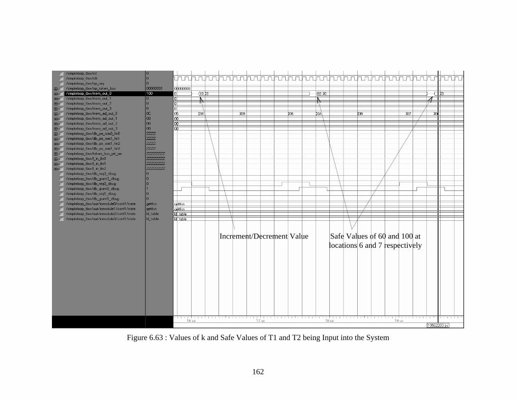
162
Figure 6.63 : Values of k and Safe Values of T1 and T2 being Input into the System
Increment/Decrement Value Safe Values of 60 and 100 at locations 6 and 7 respectively

163
When process P1 finishes, it forks to two follow on processes, P2 and P4 due to
which CE0 issues two command tokens to the PRT Mapper, which in turn allocates
Process P2 to CE1 and process P4 to CE0.This is demonstrated in Figure 6.64. The
results for P2, an unsigned value of 70, appears at the port “mem_out_1” and it is stored
at location x”03” indicated by the “mem_ad_out_1” port.
Similarly for CE0, the result of subtraction, an unsigned value of “90” appears at
“mem_out_0” port and it is stored at the address x”04” in the shared data memory. From
this point on whenever CE0 performs an operation and displays a result, the bus
“mem_out_0” should be seen for the final result and the bus “mem_ad_out_0” should be
seen for the address at which it stores the result. The same applies for the other CEs.
Once the two processes get over, the next processes P3 and P5 need to be executed.
Figure 6.65 shows the comparison process P3 being done when a command token is
issued to the PRT mapper and it issues P3 to CE0. The instruction for this can be seen as
x”9C03 3014”. As part of this process, the new value of unsigned 70 is compared with
the original value of T1, which is unsigned 100 to see if it should loop back. Since the
check comes out false, the application loops back to process P2, as per the process flow
graph. Similarly, process P5 is executed after process P4 which compares the new value
of unsigned 90 with the original value of T2, unsigned 60 to see if they are equal. The
compare fails and hence the application loops back to process P4. This is shown in
Figure 6.66.

164
Figure 6.64 : Instructions for Processes P2 and P4
Instruction for P2 done by CE1
Instruction for P4 done by CE0

165
Figure 6.65 : Process P3 being done. First Comparison Will be Performed.
Process P3

166
Figure 6.66 : Process P5 is done comparing 60 with 90
60 and 90 compared

167
As part of the first loop back, process P2 starts execution. It takes the value of unsigned
70 that was stored at location x”04” and adds the value of unsigned 10 to it again to
obtain a final result of unsigned 80 which is stores back at location x”03” in the shared
data memory. This has been illustrated in Figure 6.67. Also, as part of the loop back
process for the lower loop, when P5 loops back to P4 for the first time, the PRT mapper
allocates this process to CE0, as can be seen from Figure 6.68 and a value of unsigned
“10” is again subtracted from the new value of unsigned “90” that was earlier computed
and stored at location x”04”.This leads to a new value of unsigned “80” and as usual it is
stored back at location x”04”. Once P2 ends, P3 needs to be executed and again the
comparison of this new value calculated in P2 needs to be done. The execution of process
P3 for the second time is illustrated in Figure 6.69. This is done by CE0 as it evident from
the waveform. Also, the command token x”8102003” indicates next process is P2 again.

168
Figure 6.67 : P2 being Re-Executed as Part of First Feedback Loop
CE0 re-executes P2
70 is added with 10 to get 80

169
Figure 6.68 : First Feedback for P4 done by CE0

170
Figure 6.69 : Process P3 being Executed For the Second Time
100 is compared with 80
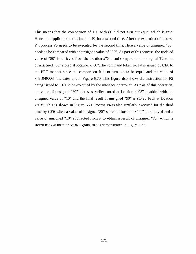
171
This means that the comparison of 100 with 80 did not turn out equal which is true.
Hence the application loops back to P2 for a second time. After the execution of process
P4, process P5 needs to be executed for the second time. Here a value of unsigned “80”
needs to be compared with an unsigned value of “60”. As part of this process, the updated
value of “80” is retrieved from the location x”04” and compared to the original T2 value
of unsigned “60” stored at location x”06”.The command token for P4 is issued by CE0 to
the PRT mapper since the comparison fails to turn out to be equal and the value of
x”81040003” indicates this in Figure 6.70. This figure also shows the instruction for P2
being issued to CE1 to be executed by the interface controller. As part of this operation,
the value of unsigned “80” that was earlier stored at location x”03” is added with the
unsigned value of “10” and the final result of unsigned “90” is stored back at location
x”03”. This is shown in Figure 6.71.Process P4 is also similarly executed for the third
time by CE0 when a value of unsigned”80” stored at location x”04” is retrieved and a
value of unsigned “10” subtracted from it to obtain a result of unsigned “70” which is
stored back at location x”04”.Again, this is demonstrated in Figure 6.72.

172
Figure 6.70 : Process P5 being Executed Second Time and the Follow on Process P4
60 at 6 is compared with 80 at 4

173
Once again, the compares at P3 and P5 need to be done. As shown in Figure 6.73,
a value of unsigned 90 is retrieved from location x”03” and it is compared with the
original value of T1, which is unsigned 60. Since the two are not equal, the compare fails
again and the application loops back to process 2.Similarlym, as part of process P5, a
value of unsigned “70” stored at location x”04” is compared with the original value of
T2, which is unsigned 60 and since they are not equal, the application loops back to P4.
Both these processes are executed by CE0. This is shown in Figure 6.74.
Next, processes P2 and P4 need to be executed again. As shown in Figure 6.75,
process P2 is executed by CE1, which retrieves the updated value of unsigned “90” and
adds the value of unsigned “10” to it to obtain a value of unsigned “100” which is stored
at location x”03” again.
Also, the process P4 is re-executed, this time, by CE0. As part of this process, it
retrieves the value of unsigned “70” from location x”04” and subtracts unsigned value of
“10” from it to obtain a final result of unsigned “60” that it stores back at location
x”04”.This has been displayed in Figure 6.76. Once this is over, process P3 is re-executed
as part of the compare process. Here a value of unsigned 100 from location x”03” is
compared for equality with the original value of T1, unsigned “100” stored at location
x”07”.This is demonstrated in Figure 6.77.

174
Figure 6.71 : Process P2 Executed 3rd Time and a Value of 90 Stored at Location x”03”

175
Figure 6.72 : Process P4 Executed 3rd Time With 70 Stored at Location x”04”

176
Figure 6.73 : Process P3 Executed 3rd Time Where 90 is Compared with 100
100 at 7 is compared with 90 at 3

177
Figure 6.74 : Process P5 done by CE0 where 70 is compared with 60

178
Figure 6.75 : Process P2 Executed 4th time by CE1 to Obtain a Result of Unsigned “100”

179
Figure 6.76 : P4 is done by CE1 - 4th Iteration. A Value of Unsigned “60” at x”04”

180
Figure 6.77 – Process P3 Final Execution and Token for P6 Issued to PRT Mapper
100 at 7 compared with 100 at 3. It matches and hence the looping stops
Command Token issued to PRT Mapper for execution of P6, the final process

181
Here, the condition for “Exit-PN” is finally satisfied as the comparison succeeds and the
token x”81068003” is issued to the PRT Mapper so that it can map it to the most
available CE to execute process P6. Also a look at the “state” signal for the interface
controller module indicates that the system has gone to the “StopL” state and successfully
broken out of the loop. The PRT Mapper now waits for the other join token that has to be
sent by process P5, once its Exit PN condition is met. Process P5 is executed by CE0 and
as indicated in Figure 6.78. As part of this process, the unsigned value of “60” at location
x”04” is compared with the original value of unsigned‘60’ at location x”06”.
The values turn out to be equal and hence the condition for the breaking out of the
loop is satisfied. CE0 issues a command token x” 81068003” indicating that the next
process is P6.The “state” signal of the controller of CE0 goes into the ‘StopL’ state
indicating this and the command is sent to the PRT Mapper for mapping it to the most
available CE, for executing process P6.
The PRT Mapper receives both these tokens and performs the join operation,
allocating the instruction to CE1 which it finds to me the most available CE at this
moment. The final values are displayed as part of this process. It can be now seen that the
values are swapped from what they were initially input at, that is, at location x”03” we
now have a value of unsigned “60” and at location x”04” we now have a value of
unsigned “100”, contrary to the initial settings. This is indicated in Figure 6.79.

182
Figure 6.78 – Process P5 Executed for Last Time and Command Token for P6
60 at 6 compared with 60 at 4. It matches and hence the looping stops
Command Token issued to PRT Mapper for execution of P6, the final process. Note the “8” in the command token indicating the Hold field is set.
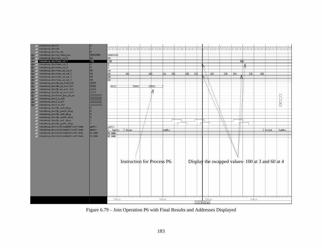
183
Figure 6.79 – Join Operation P6 with Final Results and Addresses Displayed
Instruction for Process P6. Display the swapped values- 100 at 3 and 60 at 4

184
Thus, this application shows that the system can comfortably execute process flow graphs
with multiple iteration or loops and prove very useful in systems that use such
algorithms.
Using the above described applications, it has been verified that the HDCA is
suited for Process Flow Graphs of varying complexities. It can comfortably handle cyclic
and acyclic process flow graphs of different types and execute them in a fault tolerant,
robust manner.

185
Chapter Seven Conclusions and Recommendations
7.0 Conclusion
The second phase model of the HDCA thus has lots of improvements over the
first phase model of the HDCA. A special purpose multiplier CE has now been added to
the system along with its associated controller. It can now execute applications of varied
nature and of practical importance like Convolution, Digital Down Converting and the
like. The second phase HDCA no longer possesses the limitations of the first phase,
wherein,a single process could not fork to any more than two processes.This limitation is
overcome in the second phase of the HDCA by means of a dummy process, as
demomnstrated. The second phase HDCA is also re-configure at the node level, which
helps prevent system failures when overloading of a particular node occurs. This system
meets most of the requirements imposed by the compute intense real and non real time
applications that are in use today. Besides the parallel nature of the system, its scalability
makes it ideal to be used in the aforementioned applications. The introduction of the
Interconnect Network Switch into the system further improves the HDCA by reducing
the bus contention by introducing a variable priority shared memory contention
resolution protocol. This also prevents any starvation issues from arising, making the
system more robust. Thus in the work reported here, additional enhancements have been
made to the HDCA by adding newer processors, making functional enhancements and
validating it with different kinds of complex acyclic/cyclic applications.

186
7.1 Recommendations
The following recommendations for a future third phase model would further improve the
HDCA and remove whatever restrictions remain in the current system
1) An operating system should be introduced for the HDCA. Currently, several Operating
Systems are available for embedded systems like VXWorks, Linux etc. One advantage of
having this would obviously be in handling faults and getting over them. Another big
advantage would be the system would be more automated with all the tokens for an
application being input by the system rather than the user. The data valid signal which
controls data entering the LUT would also be handled by the Operating System. It would
also help control hazards if any in the system.
2) More complex processors should be introduced. The current memory-register
computer architectures are self sufficient for providing a proof of concept. However,
when it comes down to real world applications such as weather prediction and ocean
current models etc. raw power is needed; which the simple memory-register computers
fail to provide. It would be nice to have an IBM Power PC instead of the memory-register
computer architecture. This would also mean changing the address bus widths to 32 bits
or more from 16 bits. This change would provide the designer more flexibility to design
the system. Another advantage of this would be the ability to do multiplication and
division within a single processor instead of having special purpose architectures for it.
Also, the standby CE would then be able to serve as a back-up for any of the CEs because
it would then be able to perform all operations that the existing CEs could do.
3) The token widths and the hence the bus widths should be increased beyond 32 bits.
This would allow the design of applications with a higher complexity. To cite and
example, just increasing the process number field by 1 bit allows 64 processes instead of
32. Increasing the "Exit PN" field by 2 bits allows the application to loop anywhere till
the last process. While these restrictions could be overcome by modifying the current
system by removing some bits from the other fields, it would involve a tradeoff in
reducing the number of processors that can simultaneously coexist in the system and their
corresponding physical addresses on a chip.
4) To improve performance some kind of burst mechanism could be used to transfer data
and addresses on the same bus, similar to what is done in the PCI protocol. This could

187
help take full advantage of today’s high powered processors and help improve the
performance.
5) An introduction of a cache system and replacing the current processors with their
corresponding pipelined versions could be additional steps that could be done to improve
performance as a first step, before going for the IBM Power PC processors.
6) Currently the Input Data Rom complexity varies in the order of 2 * k 2, where k is the
number of elements in the input matrix when a multiplication or a division operation is to
be done. This limitation roots in the design of the divider and multiplier bus where the
data address does not change after the data has been fetched from the data memory
causing the result to be overwritten over the original data. A provision should be
provided to get around this issue. This issue roots in the absence of a Program Counter in
the processor due to which the data address cannot be changed once its been assigned to
retrieve either the dividend or the multiplicand.

188
Appendix A VHDL Code for Post Place and Route Simulation Module Name: entirenew.vhd – Top Level Entity for the Entire HDCA System library IEEE; use IEEE.STD_LOGIC_1164.ALL; use IEEE.STD_LOGIC_ARITH.ALL; use IEEE.STD_LOGIC_UNSIGNED.ALL; -- Uncomment the following lines to use the declarations that are -- provided for instantiating Xilinx primitive components. --library UNISIM; --use UNISIM.VComponents.all; entity entiresystry2 is Port (rst,clk:in std_logic; inpt_data0,inpt_data1:in std_logic_vector(15 downto 0); idv0,idv1:in std_logic; op_req:in std_logic; Op_Token_bus: in STD_LOGIC_VECTOR (31 downto 0); Mem_out_0,Mem_out_1,Mem_out_2,Mem_out_3: out std_logic_vector ( 15 downto 0); Addr_en: in std_logic; mem_ad_out_0,mem_ad_out_1,mem_ad_out_2,mem_ad_out_3:out std_logic_vector(6 downto 0); R3_out_dbug_fin0,R3_out_dbug_fin1 : out std_logic_vector( 15 downto 0); shft_out_dbug_fin0,shft_out_dbug_fin1 : out std_logic_vector( 15 downto 0 ); dbug_st_pe_fin0,dbug_st_pe_fin1 : out std_logic_vector( 3 downto 0); dbus_sig0_fin0,dbus_sig1_fin1,dbus_sig2_fin2 : out std_logic_vector (15 downto 0); dataout_lut_fin0,dataout_lut_fin1,dataout_lut_fin2,dataout_lut_fin3:out std_logic_vector(15 downto 0); db_pe_icm0_fin0,db_pe_icm1_fin1,db_pe_icm1_fin2,db_pe_icm1_fin3 : out std_logic_vector( 15 downto 0) ; R0_out_dbug_fin0,R0_out_dbug_fin1 : out std_logic_vector(15 downto 0); token_bus_prt_pe : out std_logic_vector (31 downto 0); Wr_out_dbug0_fin0,Wr_out_dbug1_fin1 : out std_logic_vector( 1 downto 0); ce_sig0_fin0,ce_sig1_fin1: out std_logic; tbgrnt_sig0_fin0,tbgrnt_sig1_fin1 : out std_logic; tbreq_sig0_fin0,tbreq_sig1_fin1 : out std_logic; i_rdy_icm0_fin0,i_rdy_icm1_fin1 : out std_logic ; snd_i_icm0_fin0,snd_i_icm1_fin1 : out std_logic; l_in_fin0,l_in_fin1,l_in_fin2 : out std_logic_vector(31 downto 0); contrl_0,control_1 : out std_logic_vector( 3 downto 0); x_dbug_fin0,x_dbug_fin1,x_dbug_fin3 : out std_logic_vector(6 downto 0); dloutfin0,dloutfin1:out std_logic_vector(15 downto 0); count_dbug0,count_dbug1,count_dbug3:out std_logic_vector(6 downto 0); db_req3_dbug,db_grant3_dbug : out std_logic; db_req0_dbug,db_grant0_dbug : out std_logic; db_req1_dbug,db_grant1_dbug : out std_logic; RLTable0,RLTable1,RLTable2,RLTable3: out std_logic_vector( 1 downto 0); dwr0,dwr1,dwr2,dwr3: out std_logic; tabin0,tabin1,tabin2,tabin3: out std_logic; temp3_ce0,temp3_ce1 :out std_logic_vector(2 downto 0); temp2_ce0,temp2_ce1 :out std_logic_vector(1 downto 0);

189
temp1_ce0,temp1_ce1 :out std_logic_vector(1 downto 0); temp4_ce0,temp4_ce1 :out std_logic_vector(4 downto 0); temp5_ce0,temp5_ce1 :out std_logic_vector(3 downto 0); count_ce1 : out std_logic_vector (7 downto 0)); end entiresystry2; architecture Behavioral of entiresystry2 is --Begin components used in this module --PE3/CE0 component component PE is port ( Data_Bus : inout std_logic_vector(15 downto 0); R_W : out std_logic; Cntl_bus : in std_logic_vector(15 downto 0); RST, ODR, IDV : in std_logic; clk, Bus_grant : in std_logic; CInstr_rdy : in std_logic; inpt : in std_logic_vector(15 downto 0); Bus_req, Snd_Instr, Fin : out std_logic; Addr : out std_logic_vector(7 downto 0); Rq_inpt, Rq_outpt : out std_logic; STOPLOOP : out std_logic; -- added for dbugging R3_out_dbug : out std_logic_vector( 15 downto 0); shft_out_dbug : out std_logic_vector( 15 downto 0 ); dbug_st_pe : out std_logic_vector( 3 downto 0); tmp4_dbug : out std_logic_vector(15 downto 0); m5outdbg: out std_logic_vector(15 downto 0); R0_out_dbug : out std_logic_vector(15 downto 0); tmp3_dbug: out std_logic_vector(2 downto 0); tmp2_dbug: out std_logic_vector(1 downto 0); tmp1_dbug: out std_logic_vector(1 downto 0); tmp44_dbug: out std_logic_vector(4 downto 0) ; tmp5_dbug: out std_logic_vector(3 downto 0); count_out_pe : out std_logic_vector (7 downto 0) ) ; end component; --Interface controller component listing component CONTChip is generic (Chip_addr : integer := 3; Inst0 : integer := 156; Inst1 : integer := 48; Inst2 : integer := 152 ); port ( Data_bus: inout STD_LOGIC_VECTOR (15 downto 0); Chip_EN: in STD_LOGIC; Snd_i,stoplp: in std_logic; Rst: in STD_LOGIC; Clk: in STD_LOGIC; tbus_grnt: in STD_LOGIC; token_bus: inout STD_LOGIC_VECTOR (31 downto 0); tbus_req: out STD_LOGIC;

190
I_rdy: out std_logic; Avail: out STD_LOGIC_VECTOR (4 downto 0); x_dbug : out std_logic_vector(6 downto 0); count_dbug : out std_logic_vector(6 downto 0); Wr_out_dbug : out std_logic_vector (1 downto 0); R_L_Table_dbug: out STD_LOGIC_VECTOR (1 downto 0); Ld_Rd_dbug: out STD_LOGIC; ccntl_in_dbug :out std_logic_vector(24 downto 0); dataout_lut : out std_logic_vector(15 downto 0); outbuf0_dbug: out std_logic_vector(15 downto 0); outbuf1_dbug : out std_logic_vector(15 downto 0); line_out_dbug: out std_logic_vector(31 downto 0); l_in : out std_logic_vector(31 downto 0); buf_dbug : out std_logic_vector(24 downto 0); cntl_out_fin : out std_logic_vector( 3 downto 0); dlout_contchip:out std_logic_vector(15 downto 0); dwr_cont: out std_logic; tab_in_contchip: out std_logic ); end component; -- Component Listing for Process Req token mapper component Token_mapr is port ( token_bus: inout STD_LOGIC_VECTOR (31 downto 0); bus_req: inout STD_LOGIC; clk : in std_logic; rst : in std_logic; bus_grnt: in STD_LOGIC; Avail3: in STD_LOGIC_VECTOR (4 downto 0); Avail4: in STD_LOGIC_VECTOR (4 downto 0); Avail2: in STD_LOGIC_VECTOR (4 downto 0); Avail5: in STD_LOGIC_VECTOR (4 downto 0); obstemp6_prtdbug,t6_prtdbug: out std_logic_vector(22 downto 0) ); end component; -- Divider PE component Divpe is port (Cntrlr_bus : in std_logic_vector(15 downto 0); Snd_I : out std_logic; clk : in std_logic; rst : in std_logic; Instr_rdy : in std_logic; Fin : out std_logic; Data_bus : inout std_logic_vector(15 downto 0); Bus_req : out std_logic; Bus_gnt : in std_logic; Addr : out std_logic_vector(6 downto 0); R_W : buffer std_logic; loc_bus_dbug : out std_logic_vector(7 downto 0); Iaddr_bus_dbug : out std_logic_vector(7 downto 0); Iaddr_dbug : out std_logic_vector(7 downto 0); R2_out_dbug : out std_logic_vector( 7 downto 0); Imem_bus_dbug : out std_logic_vector(15 downto 0 ) );

191
end component; component multpe is Port ( mcntl_bus : in std_logic_vector(15 downto 0); Snd_I : out std_logic; clk : in std_logic; rst : in std_logic; Instr_rdy : in std_logic; Fin : out std_logic; mdata_bus : inout std_logic_vector(15 downto 0); bus_req : out std_logic; bus_gnt : in std_logic; multaddr : out std_logic_vector(7 downto 0);--Output address to shared dmem r_w : inout std_logic; cbusout_dbug : out std_logic_vector(7 downto 0); Iaddr_bus_dbug : out std_logic_vector(7 downto 0); R2out_dbug : out std_logic_vector( 7 downto 0); Imem_bus_dbug : out std_logic_vector(15 downto 0 ); mux3out_dbg:out std_logic_vector(7 downto 0); ms3dbg:out std_logic_vector(1 downto 0); ms1dbg : out std_logic; ms2dbg : out std_logic; component multpe is Port ( mcntl_bus : in std_logic_vector(15 downto 0); Snd_I : out std_logic; clk : in std_logic; rst : in std_logic; Instr_rdy : in std_logic; Fin : out std_logic; mdata_bus : inout std_logic_vector(15 downto 0); bus_req : out std_logic; bus_gnt : in std_logic; multaddr : out std_logic_vector(7 downto 0);--Output address to shared dmem r_w : inout std_logic; cbusout_dbug : out std_logic_vector(7 downto 0); Iaddr_bus_dbug : out std_logic_vector(7 downto 0); R2out_dbug : out std_logic_vector( 7 downto 0); Imem_bus_dbug : out std_logic_vector(15 downto 0 ); mux3out_dbg:out std_logic_vector(7 downto 0); ms3dbg:out std_logic_vector(1 downto 0); ms1dbg : out std_logic; ms2dbg : out std_logic; adderout_dbug : out std_logic_vector(7 downto 0); ms4dbg : out std_logic; lmd_dbg,lmr_dbg : out std_logic; ndout : out std_logic; multout_fin : out std_logic_vector( 15 downto 0); tomultr_dbg:out std_logic_vector(7 downto 0); tomultd_dbg:out std_logic_vector(7 downto 0) ); end component; component gate_ic_a is Port ( clk: in std_logic ; rst: in std_logic ;

192
ctrl: in std_logic_vector(3 downto 0) ; qdep: in std_logic_vector(19 downto 0) ; addr_bus: in std_logic_vector(27 downto 0) ; data_in0,data_in1,data_in2,data_in3 : in std_logic_vector(15 downto 0) ; rw: in std_logic_vector(3 downto 0) ; flag: inout std_logic_vector(3 downto 0) ; data_out0,data_out1,data_out2,data_out3: out std_logic_vector(15 downto 0) ); end component; --Begin signals used in the system signal dbus_sig0,dbus_sig1,dbus_sig2,dbus_sig3: std_logic_vector(15 downto 0); signal rw_sig0,rw_sig1,rw_sig2,rw_sig3: std_logic; signal db_pe_icm0,db_pe_icm1,db_pe_icm2,db_pe_icm3: std_logic_vector(15 downto 0); signal db_grant0,db_grant1,db_grant2,db_grant3:std_logic; signal i_rdy_icm0,i_rdy_icm1,i_rdy_icm2,i_rdy_icm3: std_logic; signal db_req0,db_req1,db_req2,db_req3: std_logic; signal snd_i_icm0,snd_i_icm1,snd_i_icm2,snd_i_icm3: std_logic; signal ce_sig0,ce_sig1,ce_sig2,ce_sig3:std_logic; signal addr_0,addr_1,addr_2,addr_3:std_logic_vector(7 downto 0); signal stop_lp_sig0,stop_lp_sig1: std_logic; signal tbgrnt_sig0,tbgrnt_sig1,tbgrnt_sig2,tbgrnt_sig3:std_logic ; signal tbreq_sig0,tbreq_sig1,tbreq_sig2,tbreq_sig3 : std_logic; signal avlsig0,avlsig1,avlsig2,avlsig3 : std_logic_vector( 4 downto 0); signal op_token_bus_sig : std_logic_vector(31 downto 0); signal bus_req_prt,bus_grnt_prt : std_logic; signal mem_ad : std_logic_vector (7 downto 0); signal mem_di_0,mem_di_1,mem_di_2,mem_di_3 : std_logic_vector( 15 downto 0); signal mem_do_0,mem_do_1,mem_do_2,mem_do_3 : std_logic_vector( 15 downto 0); signal m_r_w : std_logic; signal optmp_req : std_logic; signal op_gnt:std_logic; -- This was earlier set to buffer resulting in elaboration error in post-translate simulation signal odr0,odr1: std_logic; signal Rq_OPT0 : std_logic; signal Rq_OPT1 : std_logic; signal rq_ipt0,rq_ipt1 : std_logic; begin --Port Mapping for components PE3_CE0: pe port map( Data_Bus=>dbus_sig0, R_W => rw_sig0, Cntl_bus=>db_pe_icm0, RST=>rst, ODR=>odr0, IDV=>idv0, clk=>clk, Bus_grant=>db_grant0, CInstr_rdy=>I_rdy_icm0, inpt =>inpt_data0, Bus_req=>db_req0, Snd_Instr=>snd_i_icm0, Fin=>ce_sig0, Addr =>addr_0,

193
Rq_inpt=>Rq_IPT0, Rq_outpt=>Rq_OPT0, STOPLOOP =>Stop_lp_sig0, -- added for dbugging R3_out_dbug=>R3_out_dbug_fin0, shft_out_dbug=>shft_out_dbug_fin0, dbug_st_pe => dbug_st_pe_fin0, R0_out_dbug => R0_out_dbug_fin0, tmp3_dbug => temp3_ce0, tmp2_dbug => temp2_ce0, tmp1_dbug => temp1_ce0, tmp44_dbug => temp4_ce0, tmp5_dbug => temp5_ce0, count_out_pe => open ); PE2_CE1: pe port map( Data_Bus=>dbus_sig1, R_W => rw_sig1, Cntl_bus=>db_pe_icm1, RST=>rst, ODR=>odr1, IDV=> idv1, clk=>clk, Bus_grant=>db_grant1, CInstr_rdy=>I_rdy_icm1, inpt =>inpt_data1, Bus_req=>db_req1, Snd_Instr=>snd_i_icm1, Fin=>ce_sig1, Addr =>addr_1, Rq_inpt=>Rq_IPT1, Rq_outpt=>Rq_OPT1, STOPLOOP =>Stop_lp_sig1, -- added for dbugging R3_out_dbug=>R3_out_dbug_fin1, shft_out_dbug=>shft_out_dbug_fin1, dbug_st_pe => dbug_st_pe_fin1, R0_out_dbug => R0_out_dbug_fin1, tmp3_dbug => temp3_ce1, tmp2_dbug => temp2_ce1, tmp1_dbug => temp1_ce1, tmp44_dbug => temp4_ce1, tmp5_dbug => temp5_ce1, count_out_pe => count_ce1 ); Icmodule0: contchip port map( Data_bus => db_pe_icm0, Chip_EN => ce_sig0, Snd_i => snd_i_icm0, stoplp => stop_lp_sig0, Rst => rst, Clk =>clk, tbus_grnt =>tbgrnt_sig0, token_bus =>op_token_bus_sig, tbus_req =>tbreq_sig0, I_rdy =>I_rdy_icm0, Avail =>avlsig0,

194
x_dbug =>x_dbug_fin0, count_dbug =>count_dbug0, Wr_out_dbug =>Wr_out_dbug0_fin0, R_L_Table_dbug =>RLTable0, Ld_Rd_dbug =>open, dataout_lut =>dataout_lut_fin0, outbuf0_dbug =>open, outbuf1_dbug =>open, line_out_dbug =>open, l_in =>l_in_fin0, buf_dbug => open , ccntl_in_dbug => open, cntl_out_fin => control_0, dlout_contchip=>dloutfin0, dwr_cont=>dwr0, tab_in_contchip => tabin0 ); Icmodule1: contchip Generic map (chip_addr =>2, Inst0=> 156, Inst1=> 48, Inst2=> 152) port map( Data_bus => db_pe_icm1, Chip_EN => ce_sig1, Snd_i => snd_i_icm1, stoplp => stop_lp_sig1, Rst => rst, Clk =>clk, tbus_grnt =>tbgrnt_sig1, token_bus =>op_token_bus_sig, tbus_req =>tbreq_sig1, I_rdy =>I_rdy_icm1, Avail =>avlsig1, x_dbug =>x_dbug_fin1, count_dbug =>count_dbug1, Wr_out_dbug =>Wr_out_dbug1_fin1, R_L_Table_dbug =>RLTable1, Ld_Rd_dbug =>open, dataout_lut =>dataout_lut_fin1, outbuf0_dbug =>open, outbuf1_dbug =>open, line_out_dbug =>open, l_in =>l_in_fin1 , buf_dbug => open, ccntl_in_dbug => open, cntl_out_fin => control_1, dlout_contchip=>dloutfin1, dwr_cont=>dwr1, tab_in_contchip => tabin1 ); -- port mapping for interface controller module for div chip Icmodule2: contchip Generic map (chip_addr => 4, Inst0=> 142, Inst1=> 255, Inst2=> 142)
195
port map( Data_bus => db_pe_icm2, Chip_EN => ce_sig2, Snd_i => snd_i_icm2, stoplp => '0', Rst => rst, Clk =>clk, tbus_grnt =>tbgrnt_sig2, token_bus =>op_token_bus_sig, tbus_req =>tbreq_sig2, I_rdy =>I_rdy_icm2, Avail =>avlsig2, x_dbug =>open, count_dbug =>open, Wr_out_dbug =>open, R_L_Table_dbug =>RLTable2, Ld_Rd_dbug =>open, dataout_lut =>dataout_lut_fin2, outbuf0_dbug =>open, outbuf1_dbug =>open, line_out_dbug =>open, l_in =>l_in_fin2 , buf_dbug => open, ccntl_in_dbug => open, dwr_cont=>dwr2, tab_in_contchip => tabin2 ); Icmodule3: contchip Generic map (chip_addr => 5, Inst0=> 142, Inst1=> 255, Inst2=> 142) port map( Data_bus => db_pe_icm3, Chip_EN => ce_sig3, Snd_i => snd_i_icm3, stoplp => '0', Rst => rst, Clk =>clk, tbus_grnt =>tbgrnt_sig3, token_bus =>op_token_bus_sig, tbus_req =>tbreq_sig3, I_rdy =>I_rdy_icm3, Avail =>avlsig3, x_dbug =>x_dbug_fin3, count_dbug =>count_dbug3, Wr_out_dbug =>open, R_L_Table_dbug =>RLTable3, Ld_Rd_dbug =>open, dataout_lut =>dataout_lut_fin3, outbuf0_dbug =>open, outbuf1_dbug =>open, line_out_dbug =>open, l_in =>open, buf_dbug => open, ccntl_in_dbug => open, dwr_cont=>dwr3, tab_in_contchip => tabin3 );

196
prtmapper: token_mapr port map( token_bus =>Op_token_bus_sig, bus_req=>bus_req_prt, clk =>clk, rst =>rst, bus_grnt =>bus_grnt_prt, Avail3 =>avlsig0, Avail4 => avlsig2, Avail2 =>avlsig1, Avail5 => avlsig3, temp6_prtdbug=>open, t6_prtdbug=>open ); DIV1 : divpe port map(Cntrlr_bus=>db_pe_icm2, Snd_I=> snd_i_icm2, clk => clk, rst => rst, Instr_rdy => I_rdy_icm2, Fin => ce_sig2, Data_bus => dbus_sig2, Bus_req => db_req2, Bus_gnt => db_grant2, Addr => addr_2(6 downto 0), R_W => rw_sig2, loc_bus_dbug => open, Iaddr_bus_dbug => open, Iaddr_dbug => open, R2_out_dbug => open, Imem_bus_dbug => open ); multpemap: multpe port map ( mcntl_bus => db_pe_icm3, Snd_I => snd_i_icm3, clk =>clk, rst =>rst, Instr_rdy =>i_rdy_icm3, Fin =>ce_sig3, mdata_bus =>dbus_sig3, bus_req =>db_req3, bus_gnt =>db_grant3, multaddr =>addr_3, r_w =>rw_sig3, cbusout_dbug => open, Iaddr_bus_dbug => open, R2out_dbug => open, Imem_bus_dbug =>open, mux3out_dbg=> open, ms3dbg=> open, ms1dbg => open, ms2dbg => open , adderout_dbug => open,

197
ms4dbg => open, lmd_dbg=> open, lmr_dbg => open, ndout => open, multout_fin => open, tomultr_dbg=> open, tomultd_dbg=> open ); IC_gate: gate_ic_a Port map ( clk => clk, rst => rst, ctrl(0) => db_req0, ctrl(1) => db_req1, ctrl(2) => db_req2, ctrl(3) => db_req3, qdep(4 downto 0) => avlsig0, qdep(9 downto 5) => avlsig1, qdep(14 downto 10)=> avlsig2, qdep(19 downto 15)=> avlsig3, addr_bus(6 downto 0) => addr_0(6 downto 0), addr_bus(13 downto 7) => addr_1(6 downto 0), addr_bus(20 downto 14) => addr_2(6 downto 0), addr_bus(27 downto 21) => addr_3(6 downto 0), data_in0 => mem_di_0, data_in1 => mem_di_1, data_in2 => mem_di_2, data_in3 => mem_di_3, rw(0) => rw_sig0, rw(1) => rw_sig1, rw(2) => rw_sig2, rw(3) => rw_sig3, flag(0) => db_grant0, flag(1) => db_grant1, flag(2) => db_grant2, flag(3) => db_grant3, data_out0 => mem_do_0, data_out1 => mem_do_1, data_out2 => mem_do_2, data_out3 => mem_do_3 ); -- signals taken out for dbugging dbus_sig0_fin0 <= dbus_sig0; dbus_sig1_fin1 <= dbus_sig1; dbus_sig2_fin2 <= dbus_sig2; db_pe_icm0_fin0 <= db_pe_icm0; db_pe_icm1_fin1 <= db_pe_icm1; db_pe_icm1_fin2 <= db_pe_icm2; db_pe_icm1_fin3 <= db_pe_icm3; token_bus_prt_pe <= Op_token_bus_sig; ce_sig1_fin1 <= ce_sig1; ce_sig0_fin0 <= ce_sig0; tbgrnt_sig0_fin0 <= tbgrnt_sig0; tbgrnt_sig1_fin1 <= tbgrnt_sig1; tbreq_sig0_fin0 <= tbreq_sig0; tbreq_sig1_fin1 <= tbreq_sig1;
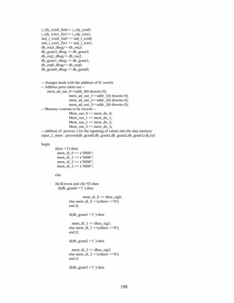
198
i_rdy_icm0_fin0<= i_rdy_icm0; i_rdy_icm1_fin1<= i_rdy_icm1; snd_i_icm0_fin0 <= snd_i_icm0; snd_i_icm1_fin1 <= snd_i_icm1; db_req3_dbug<= db_req3; db_grant3_dbug <= db_grant3; db_req1_dbug<= db_req1; db_grant1_dbug <= db_grant1; db_req0_dbug<= db_req0; db_grant0_dbug <= db_grant0; -- changes made with the addition of IC switch -- Address ports taken out -- mem_ad_out_0<=addr_0(6 downto 0); mem_ad_out_1<=addr_1(6 downto 0); mem_ad_out_2<=addr_2(6 downto 0); mem_ad_out_3<=addr_3(6 downto 0); -- Memory contents to be viewed -- Mem_out_0 <= mem_do_0; Mem_out_1 <= mem_do_1; Mem_out_2 <= mem_do_2; Mem_out_3 <= mem_do_3; -- addition of process 1 for the inputting of values into the data memory input_2_mem : process(db_grant0,db_grant1,db_grant2,db_grant3,clk,rst) begin if(rst ='1') then mem_di_0 <= x"0000"; mem_di_1 <= x"0000"; mem_di_2 <= x"0000"; mem_di_3 <= x"0000"; else if(clk'event and clk='0') then if(db_grant0 ='1' ) then mem_di_0 <= dbus_sig0; else mem_di_0 <=(others =>'0'); end if; if(db_grant1 ='1' ) then mem_di_1 <= dbus_sig1; else mem_di_1 <=(others =>'0'); end if; if(db_grant2 ='1' ) then mem_di_2 <= dbus_sig2; else mem_di_2 <=(others =>'0'); end if; if(db_grant3 ='1' ) then

199
mem_di_3 <= dbus_sig3; else mem_di_3 <=(others =>'0'); end if; end if; end if; end process input_2_mem; -- process 2 for outputting the values from data memory output_from_mem : process(db_grant0,db_grant1,db_grant2,db_grant3,rw_sig0,rw_sig1,rw_sig2, rw_sig3,clk,rst) begin if(rst='1') then dbus_sig0 <= x"0000"; dbus_sig1 <= x"0000"; dbus_sig2 <= x"0000"; dbus_sig3 <= x"0000"; else if(clk'event and clk='0') then if(db_grant0 ='1' and rw_sig0 ='0') then dbus_sig0 <= mem_do_0; else dbus_sig0 <=(others =>'Z'); end if; if(db_grant1 ='1' and rw_sig1 ='0') then dbus_sig1 <= mem_do_1; else dbus_sig1 <=(others =>'Z'); end if; if(db_grant2 ='1' and rw_sig2 ='0') then dbus_sig2 <= mem_do_2; else dbus_sig2 <=(others =>'Z'); end if; if(db_grant3 ='1' and rw_sig3 ='0') then dbus_sig3 <= mem_do_3; else dbus_sig3 <=(others =>'Z'); end if; end if; end if; end process output_from_mem; -- end of process 2 -- Token bus logic optmp_req <= Op_req; Tknbuslg : process (tbreq_sig0,tbgrnt_sig0,bus_req_prt,bus_grnt_prt,tbreq_sig1,

200
tbgrnt_sig1,tbreq_sig2,tbgrnt_sig2,tbgrnt_sig3,tbreq_sig3,Optmp_req,Op_gnt, rst) begin if rst = '1' then tbgrnt_sig0 <= '0'; bus_grnt_prt <= '0'; tbgrnt_sig1 <= '0'; tbgrnt_sig2 <= '0'; tbgrnt_sig3 <= '0'; Op_gnt <= '0'; elsif (bus_req_prt ='1')and (tbgrnt_sig0='0') and(tbgrnt_sig1='0') and (tbgrnt_sig2='0')and(Op_gnt='0') and (tbgrnt_sig3='0') then tbgrnt_sig0 <= '0'; bus_grnt_prt <= '1'; tbgrnt_sig2 <= '0'; tbgrnt_sig1 <= '0'; tbgrnt_sig3 <= '0'; Op_gnt <= '0'; elsif (Optmp_req ='1') and (bus_grnt_prt ='0') and (tbgrnt_sig0='0') and (tbgrnt_sig1='0') and (tbgrnt_sig2='0') and (tbgrnt_sig3 ='0')then tbgrnt_sig0 <= '0'; bus_grnt_prt <= '0'; tbgrnt_sig1 <= '0'; tbgrnt_sig2 <= '0'; tbgrnt_sig3 <= '0'; Op_gnt <= '1'; elsif (tbreq_sig0 = '1') and (bus_grnt_prt='0') and (Op_gnt='0') and (tbgrnt_sig2='0')and (tbgrnt_sig1='0') and (tbgrnt_sig3 ='0') then tbgrnt_sig0 <= '1'; bus_grnt_prt <= '0'; tbgrnt_sig2 <= '0'; tbgrnt_sig1 <= '0'; tbgrnt_sig3 <= '0'; Op_gnt <= '0'; elsif (tbreq_sig2='1') and (bus_grnt_prt='0') and (Op_gnt='0') and (tbgrnt_sig0='0') and (tbgrnt_sig1='0') and (tbgrnt_sig3 ='0') then tbgrnt_sig0 <= '0'; bus_grnt_prt <= '0'; tbgrnt_sig2 <='1'; tbgrnt_sig1 <= '0'; tbgrnt_sig3 <= '0'; Op_gnt <= '0'; elsif (tbreq_sig1='1') and (bus_grnt_prt='0') and (Op_gnt='0') and (tbgrnt_sig0='0') and (tbgrnt_sig2='0')and (tbgrnt_sig3='0') then tbgrnt_sig0 <= '0'; bus_grnt_prt <= '0'; tbgrnt_sig2<='0'; tbgrnt_sig1 <= '1'; tbgrnt_sig3 <= '0'; Op_gnt <= '0'; elsif (tbreq_sig3='1') and (bus_grnt_prt='0') and (Op_gnt='0') and (tbgrnt_sig0='0') and (tbgrnt_sig2='0')and (tbgrnt_sig1='0') then tbgrnt_sig0 <= '0'; bus_grnt_prt <= '0'; tbgrnt_sig2<='0'; tbgrnt_sig1 <= '0'; tbgrnt_sig3 <= '1';

201
Op_gnt <= '0'; end if; if (bus_req_prt = '0') then bus_grnt_prt <= '0'; end if; if (Optmp_req = '0') then Op_gnt <= '0'; end if; if (tbreq_sig0 = '0') then tbgrnt_sig0 <= '0'; end if; if (tbreq_sig2 = '0') then tbgrnt_sig2 <= '0'; end if; if (tbreq_sig1 = '0') then tbgrnt_sig1 <= '0'; end if; if (tbreq_sig3 = '0') then tbgrnt_sig3 <= '0'; end if; end process; arbiter_logic: process(clk,rst) begin if rst = '1' then odr0<='0'; odr1<='0'; elsif (clk'event and clk='1') then case rq_opt0 is when '1' => odr0 <= '1'; when '0' => odr0 <= '0'; when others => end case; case rq_opt1 is when '1' => odr1 <= '1'; when '0' => odr1 <= '0'; when others => end case; end if; end process arbiter_logic; Op_token_bus_sig <= Op_token_bus when Op_gnt = '1' else (others=>'Z'); end Behavioral; adderout_dbug : out std_logic_vector(7 downto 0); ms4dbg : out std_logic; lmd_dbg,lmr_dbg : out std_logic; ndout : out std_logic; multout_fin : out std_logic_vector( 15 downto 0); tomultr_dbg:out std_logic_vector(7 downto 0); tomultd_dbg:out std_logic_vector(7 downto 0) ); end component; component gate_ic_a is

202
Port ( clk: in std_logic ; rst: in std_logic ; ctrl: in std_logic_vector(3 downto 0) ; qdep: in std_logic_vector(19 downto 0) ; addr_bus: in std_logic_vector(27 downto 0) ; data_in0,data_in1,data_in2,data_in3 : in std_logic_vector(15 downto 0) ; rw: in std_logic_vector(3 downto 0) ; flag: inout std_logic_vector(3 downto 0) ; data_out0,data_out1,data_out2,data_out3: out std_logic_vector(15 downto 0) -- f_s_out0,f_s_out1,f_s_out2,f_s_out3 : out std_logic_vector(3 downto 0); -- dco_out0,dco_out1,dco_out2,dco_out3 : out std_logic_vector(3 downto 0) ); end component; -- --Begin signals used in the system signal dbus_sig0,dbus_sig1,dbus_sig2,dbus_sig3: std_logic_vector(15 downto 0); signal rw_sig0,rw_sig1,rw_sig2,rw_sig3: std_logic; signal db_pe_icm0,db_pe_icm1,db_pe_icm2,db_pe_icm3: std_logic_vector(15 downto 0); signal db_grant0,db_grant1,db_grant2,db_grant3:std_logic; signal i_rdy_icm0,i_rdy_icm1,i_rdy_icm2,i_rdy_icm3: std_logic; signal db_req0,db_req1,db_req2,db_req3: std_logic; signal snd_i_icm0,snd_i_icm1,snd_i_icm2,snd_i_icm3: std_logic; signal ce_sig0,ce_sig1,ce_sig2,ce_sig3:std_logic; signal addr_0,addr_1,addr_2,addr_3:std_logic_vector(7 downto 0); signal stop_lp_sig0,stop_lp_sig1: std_logic; signal tbgrnt_sig0,tbgrnt_sig1,tbgrnt_sig2,tbgrnt_sig3:std_logic ; signal tbreq_sig0,tbreq_sig1,tbreq_sig2,tbreq_sig3 : std_logic; signal avlsig0,avlsig1,avlsig2,avlsig3 : std_logic_vector( 4 downto 0); signal op_token_bus_sig : std_logic_vector(31 downto 0); signal bus_req_prt,bus_grnt_prt : std_logic; signal mem_ad : std_logic_vector (7 downto 0); signal mem_di_0,mem_di_1,mem_di_2,mem_di_3 : std_logic_vector( 15 downto 0); signal mem_do_0,mem_do_1,mem_do_2,mem_do_3 : std_logic_vector( 15 downto 0); signal m_r_w : std_logic; signal optmp_req : std_logic; signal op_gnt:std_logic; -- This was earlier set to buffer resulting in elaboration error in post-translate simulation signal odr0,odr1: std_logic; signal Rq_OPT0 : std_logic; signal Rq_OPT1 : std_logic; signal rq_ipt0,rq_ipt1 : std_logic; --signal idv0, idv1 : std_logic; --signal token_bus_prt_pe_sig :std_logic_vector(31 downto 0); begin --Port Mapping for components PE3_CE0: pe port map( Data_Bus=>dbus_sig0, R_W => rw_sig0, Cntl_bus=>db_pe_icm0, RST=>rst, ODR=>odr0, IDV=>idv0, clk=>clk,

203
Bus_grant=>db_grant0, CInstr_rdy=>I_rdy_icm0, inpt =>inpt_data0, Bus_req=>db_req0, Snd_Instr=>snd_i_icm0, Fin=>ce_sig0, Addr =>addr_0, Rq_inpt=>Rq_IPT0, Rq_outpt=>Rq_OPT0, STOPLOOP =>Stop_lp_sig0, -- added for dbugging R3_out_dbug=>R3_out_dbug_fin0, shft_out_dbug=>shft_out_dbug_fin0, dbug_st_pe => dbug_st_pe_fin0, R0_out_dbug => R0_out_dbug_fin0, tmp3_dbug => temp3_ce0, tmp2_dbug => temp2_ce0, tmp1_dbug => temp1_ce0 , tmp44_dbug => temp4_ce0, tmp5_dbug => temp5_ce0 , count_out_pe => open -- tmp6_dbug => temp6_ce0 ); PE2_CE1: pe port map( Data_Bus=>dbus_sig1, R_W => rw_sig1, Cntl_bus=>db_pe_icm1, RST=>rst, ODR=>odr1, IDV=> idv1, clk=>clk, Bus_grant=>db_grant1, CInstr_rdy=>I_rdy_icm1, inpt =>inpt_data1, Bus_req=>db_req1, Snd_Instr=>snd_i_icm1, Fin=>ce_sig1, Addr =>addr_1, Rq_inpt=>Rq_IPT1, Rq_outpt=>Rq_OPT1, STOPLOOP =>Stop_lp_sig1, -- added for dbugging R3_out_dbug=>R3_out_dbug_fin1, shft_out_dbug=>shft_out_dbug_fin1, dbug_st_pe => dbug_st_pe_fin1, R0_out_dbug => R0_out_dbug_fin1, tmp3_dbug => temp3_ce1, tmp2_dbug => temp2_ce1, tmp1_dbug => temp1_ce1, tmp44_dbug => temp4_ce1, tmp5_dbug => temp5_ce1 , count_out_pe => count_ce1 -- tmp6_dbug => temp6_ce1 ); Icmodule0: contchip port map( Data_bus => db_pe_icm0, Chip_EN => ce_sig0,

204
Snd_i => snd_i_icm0, stoplp => stop_lp_sig0, Rst => rst, Clk =>clk, tbus_grnt =>tbgrnt_sig0, token_bus =>op_token_bus_sig, tbus_req =>tbreq_sig0, I_rdy =>I_rdy_icm0, Avail =>avlsig0, x_dbug =>x_dbug_fin0, count_dbug =>count_dbug0, Wr_out_dbug =>Wr_out_dbug0_fin0, R_L_Table_dbug =>RLTable0, Ld_Rd_dbug =>open, dataout_lut =>dataout_lut_fin0, outbuf0_dbug =>open, outbuf1_dbug =>open, --line_out_dbug =>line_out_dbug_fin0, line_out_dbug =>open, l_in =>l_in_fin0, --buf_dbug => buf_dbug_fin0 , buf_dbug => open , --ccntl_in_dbug => ccntl_in_fin0, ccntl_in_dbug => open, cntl_out_fin => control_0, dlout_contchip=>dloutfin0, dwr_cont=>dwr0, tab_in_contchip => tabin0 ); Icmodule1: contchip Generic map (chip_addr =>2,Inst0=> 156, Inst1=> 48, Inst2=> 152) port map( Data_bus => db_pe_icm1, Chip_EN => ce_sig1, Snd_i => snd_i_icm1, stoplp => stop_lp_sig1, Rst => rst, Clk =>clk, tbus_grnt =>tbgrnt_sig1, token_bus =>op_token_bus_sig, tbus_req =>tbreq_sig1, I_rdy =>I_rdy_icm1, Avail =>avlsig1, x_dbug =>x_dbug_fin1, count_dbug =>count_dbug1, Wr_out_dbug =>Wr_out_dbug1_fin1, R_L_Table_dbug =>RLTable1, Ld_Rd_dbug =>open, dataout_lut =>dataout_lut_fin1, outbuf0_dbug =>open, outbuf1_dbug =>open, --line_out_dbug =>line_out_dbug_fin1, line_out_dbug =>open, l_in =>l_in_fin1 , --buf_dbug => buf_dbug_fin1, buf_dbug => open,
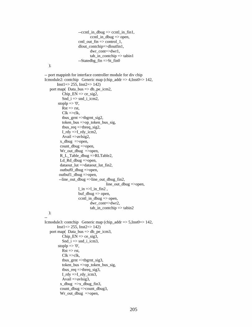
205
--ccntl_in_dbug => ccntl_in_fin1, ccntl_in_dbug => open, cntl_out_fin => control_1, dlout_contchip=>dloutfin1, dwr_cont=>dwr1, tab_in_contchip => tabin1 --Statedbg_fin =>St_fin0 ); -- port mappinh for interface controller module for div chip Icmodule2: contchip Generic map (chip_addr => 4,Inst0=> 142, Inst1=> 255, Inst2=> 142) port map( Data_bus => db_pe_icm2, Chip_EN => ce_sig2, Snd_i => snd_i_icm2, stoplp => '0', Rst => rst, Clk =>clk, tbus_grnt =>tbgrnt_sig2, token_bus =>op_token_bus_sig, tbus_req =>tbreq_sig2, I_rdy =>I_rdy_icm2, Avail =>avlsig2, x_dbug =>open, count_dbug =>open, Wr_out_dbug =>open, R_L_Table_dbug =>RLTable2, Ld_Rd_dbug =>open, dataout_lut =>dataout_lut_fin2, outbuf0_dbug =>open, outbuf1_dbug =>open, --line_out_dbug =>line_out_dbug_fin2, line_out_dbug =>open, l_in =>l_in_fin2 , buf_dbug => open, ccntl_in_dbug => open, dwr_cont=>dwr2, tab_in_contchip => tabin2 ); -- Icmodule3: contchip Generic map (chip_addr => 5,Inst0=> 142, Inst1=> 255, Inst2=> 142) port map( Data_bus => db_pe_icm3, Chip_EN => ce_sig3, Snd_i => snd_i_icm3, stoplp => '0', Rst => rst, Clk =>clk, tbus_grnt =>tbgrnt_sig3, token_bus =>op_token_bus_sig, tbus_req =>tbreq_sig3, I_rdy =>I_rdy_icm3, Avail =>avlsig3, x_dbug =>x_dbug_fin3, count_dbug =>count_dbug3, Wr_out_dbug =>open,

206
R_L_Table_dbug =>RLTable3, Ld_Rd_dbug =>open, dataout_lut =>dataout_lut_fin3, outbuf0_dbug =>open, outbuf1_dbug =>open, --line_out_dbug =>line_out_dbug_fin3, line_out_dbug =>open, l_in =>open, buf_dbug => open, ccntl_in_dbug => open, dwr_cont=>dwr3, tab_in_contchip => tabin3 ); prtmapper: token_mapr port map( token_bus =>Op_token_bus_sig, bus_req=>bus_req_prt, clk =>clk, rst =>rst, bus_grnt =>bus_grnt_prt, Avail3 =>avlsig0, Avail4 => avlsig2, Avail2 =>avlsig1, Avail5 => avlsig3, --obstemp6_prtdbug=>obstemp6_prtdbug_fin, obstemp6_prtdbug=>open, --t6_prtdbug=>t6_prtdbug_fin t6_prtdbug=>open ); -- Port map to the shared core generated Data Memory. --datamem : proc_dmem port map (addr => Mem_ad(4 downto 0),clk => clk,din => Mem_di, -- dout => Mem_do, we => M_R_W); -- port map to the divider and interface controller module DIV1 : divpe port map(Cntrlr_bus=>db_pe_icm2, Snd_I=> snd_i_icm2, clk => clk, rst => rst, Instr_rdy => I_rdy_icm2, Fin => ce_sig2, Data_bus => dbus_sig2, Bus_req => db_req2, Bus_gnt => db_grant2, Addr => addr_2(6 downto 0), R_W => rw_sig2, loc_bus_dbug => open, Iaddr_bus_dbug => open, Iaddr_dbug => open, R2_out_dbug => open, Imem_bus_dbug => open ); multpemap: multpe port map

207
( mcntl_bus => db_pe_icm3, Snd_I => snd_i_icm3, clk =>clk, rst =>rst, Instr_rdy =>i_rdy_icm3, Fin =>ce_sig3, mdata_bus =>dbus_sig3, bus_req =>db_req3, bus_gnt =>db_grant3, multaddr =>addr_3, r_w =>rw_sig3, cbusout_dbug => open, Iaddr_bus_dbug => open, --Iaddr_dbug : out std_logic_vector(7 downto 0); R2out_dbug => open, Imem_bus_dbug =>open, mux3out_dbg=> open, ms3dbg=> open, ms1dbg => open, ms2dbg => open , adderout_dbug => open, ms4dbg => open, lmd_dbg=> open, lmr_dbg => open, ndout => open, --multout_fin => mult_dbug, multout_fin => open, tomultr_dbg=> open, tomultd_dbg=> open ); IC_gate: gate_ic_a Port map ( clk => clk, rst => rst, ctrl(0) => db_req0, ctrl(1) => db_req1, ctrl(2) => db_req2, ctrl(3) => db_req3, qdep(4 downto 0) => avlsig0, qdep(9 downto 5) => avlsig1, qdep(14 downto 10)=> avlsig2, qdep(19 downto 15)=> avlsig3, addr_bus(6 downto 0) => addr_0(6 downto 0), addr_bus(13 downto 7) => addr_1(6 downto 0), addr_bus(20 downto 14) => addr_2(6 downto 0), addr_bus(27 downto 21) => addr_3(6 downto 0), data_in0 => mem_di_0, data_in1 => mem_di_1, data_in2 => mem_di_2, data_in3 => mem_di_3, rw(0) => rw_sig0, rw(1) => rw_sig1, rw(2) => rw_sig2, rw(3) => rw_sig3,
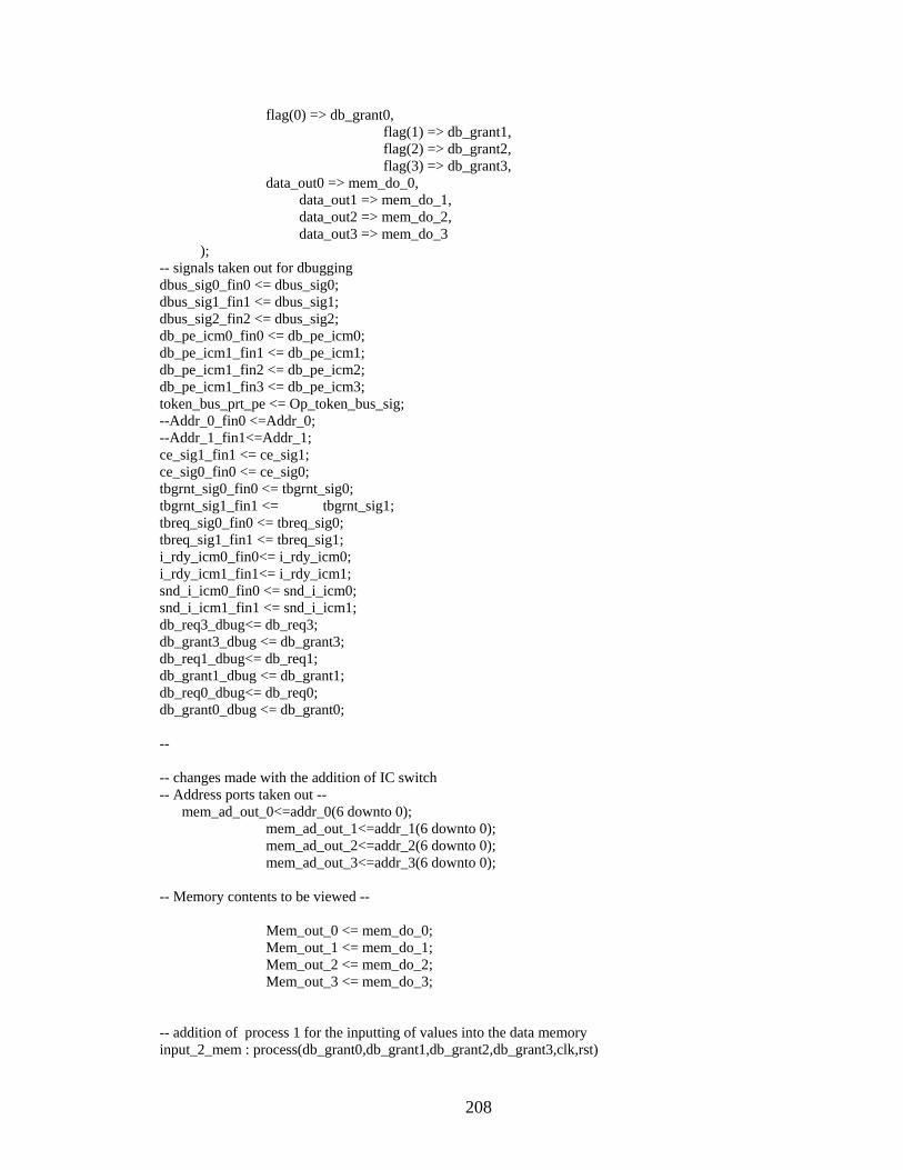
208
flag(0) => db_grant0, flag(1) => db_grant1, flag(2) => db_grant2, flag(3) => db_grant3, data_out0 => mem_do_0, data_out1 => mem_do_1, data_out2 => mem_do_2, data_out3 => mem_do_3 ); -- signals taken out for dbugging dbus_sig0_fin0 <= dbus_sig0; dbus_sig1_fin1 <= dbus_sig1; dbus_sig2_fin2 <= dbus_sig2; db_pe_icm0_fin0 <= db_pe_icm0; db_pe_icm1_fin1 <= db_pe_icm1; db_pe_icm1_fin2 <= db_pe_icm2; db_pe_icm1_fin3 <= db_pe_icm3; token_bus_prt_pe <= Op_token_bus_sig; --Addr_0_fin0 <=Addr_0; --Addr_1_fin1<=Addr_1; ce_sig1_fin1 <= ce_sig1; ce_sig0_fin0 <= ce_sig0; tbgrnt_sig0_fin0 <= tbgrnt_sig0; tbgrnt_sig1_fin1 <= tbgrnt_sig1; tbreq_sig0_fin0 <= tbreq_sig0; tbreq_sig1_fin1 <= tbreq_sig1; i_rdy_icm0_fin0<= i_rdy_icm0; i_rdy_icm1_fin1<= i_rdy_icm1; snd_i_icm0_fin0 <= snd_i_icm0; snd_i_icm1_fin1 <= snd_i_icm1; db_req3_dbug<= db_req3; db_grant3_dbug <= db_grant3; db_req1_dbug<= db_req1; db_grant1_dbug <= db_grant1; db_req0_dbug<= db_req0; db_grant0_dbug <= db_grant0; -- -- changes made with the addition of IC switch -- Address ports taken out -- mem_ad_out_0<=addr_0(6 downto 0); mem_ad_out_1<=addr_1(6 downto 0); mem_ad_out_2<=addr_2(6 downto 0); mem_ad_out_3<=addr_3(6 downto 0); -- Memory contents to be viewed -- Mem_out_0 <= mem_do_0; Mem_out_1 <= mem_do_1; Mem_out_2 <= mem_do_2; Mem_out_3 <= mem_do_3; -- addition of process 1 for the inputting of values into the data memory input_2_mem : process(db_grant0,db_grant1,db_grant2,db_grant3,clk,rst)

209
begin if(rst ='1') then mem_di_0 <= x"0000"; mem_di_1 <= x"0000"; mem_di_2 <= x"0000"; mem_di_3 <= x"0000"; else if(clk'event and clk='0') then if(db_grant0 ='1' ) then mem_di_0 <= dbus_sig0; else mem_di_0 <=(others =>'0'); end if; if(db_grant1 ='1' ) then mem_di_1 <= dbus_sig1; else mem_di_1 <=(others =>'0'); end if; if(db_grant2 ='1' ) then mem_di_2 <= dbus_sig2; else mem_di_2 <=(others =>'0'); end if; if(db_grant3 ='1' ) then mem_di_3 <= dbus_sig3; else mem_di_3 <=(others =>'0'); end if; end if; end if; end process input_2_mem; -- end of process 1 -- end of changes made ---- -- process 2 for outputting the values from data memory output_from_mem : process(db_grant0,db_grant1,db_grant2,db_grant3,rw_sig0,rw_sig1,rw_sig2, rw_sig3,clk,rst) begin if(rst='1') then dbus_sig0 <= x"0000"; dbus_sig1 <= x"0000"; dbus_sig2 <= x"0000"; dbus_sig3 <= x"0000"; else

210
if(clk'event and clk='0') then if(db_grant0 ='1' and rw_sig0 ='0') then dbus_sig0 <= mem_do_0; else dbus_sig0 <=(others =>'Z'); end if; if(db_grant1 ='1' and rw_sig1 ='0') then dbus_sig1 <= mem_do_1; else dbus_sig1 <=(others =>'Z'); end if; if(db_grant2 ='1' and rw_sig2 ='0') then dbus_sig2 <= mem_do_2; else dbus_sig2 <=(others =>'Z'); end if; if(db_grant3 ='1' and rw_sig3 ='0') then dbus_sig3 <= mem_do_3; else dbus_sig3 <=(others =>'Z'); end if; end if; end if; end process output_from_mem; -- end of process 2 -- Token bus logic optmp_req <= Op_req; Tknbuslg : process (tbreq_sig0,tbgrnt_sig0,bus_req_prt,bus_grnt_prt,tbreq_sig1, tbgrnt_sig1,tbreq_sig2,tbgrnt_sig2,tbgrnt_sig3,tbreq_sig3,Optmp_req,Op_gnt, rst) begin if rst = '1' then tbgrnt_sig0 <= '0'; bus_grnt_prt <= '0'; --Tbs4_gnt <= '0'; tbgrnt_sig1 <= '0'; tbgrnt_sig2 <= '0'; tbgrnt_sig3 <= '0'; Op_gnt <= '0'; elsif (bus_req_prt ='1')and (tbgrnt_sig0='0') and(tbgrnt_sig1='0') and (tbgrnt_sig2='0')and(Op_gnt='0') and (tbgrnt_sig3='0') then tbgrnt_sig0 <= '0'; bus_grnt_prt <= '1'; --Tbs4_gnt <= '0'; tbgrnt_sig2 <= '0'; tbgrnt_sig1 <= '0'; tbgrnt_sig3 <= '0'; Op_gnt <= '0'; elsif (Optmp_req ='1') and (bus_grnt_prt ='0') and (tbgrnt_sig0='0') and (tbgrnt_sig1='0') and (tbgrnt_sig2='0') and (tbgrnt_sig3 ='0')then

211
tbgrnt_sig0 <= '0'; bus_grnt_prt <= '0'; --Tbs4_gnt <= '0'; tbgrnt_sig1 <= '0'; tbgrnt_sig2 <= '0'; tbgrnt_sig3 <= '0'; Op_gnt <= '1'; elsif (tbreq_sig0 = '1') and (bus_grnt_prt='0') and (Op_gnt='0') and (tbgrnt_sig2='0')and (tbgrnt_sig1='0') and (tbgrnt_sig3 ='0') then tbgrnt_sig0 <= '1'; bus_grnt_prt <= '0'; --Tbs4_gnt <= '0'; tbgrnt_sig2 <= '0'; tbgrnt_sig1 <= '0'; tbgrnt_sig3 <= '0'; Op_gnt <= '0'; elsif (tbreq_sig2='1') and (bus_grnt_prt='0') and (Op_gnt='0') and (tbgrnt_sig0='0') and (tbgrnt_sig1='0') and (tbgrnt_sig3 ='0') then tbgrnt_sig0 <= '0'; bus_grnt_prt <= '0'; --Tbs4_gnt <= '1'; tbgrnt_sig2 <='1'; tbgrnt_sig1 <= '0'; tbgrnt_sig3 <= '0'; Op_gnt <= '0'; elsif (tbreq_sig1='1') and (bus_grnt_prt='0') and (Op_gnt='0') and (tbgrnt_sig0='0') and (tbgrnt_sig2='0')and (tbgrnt_sig3='0') then tbgrnt_sig0 <= '0'; bus_grnt_prt <= '0'; -- Tbs4_gnt <= '0'; tbgrnt_sig2<='0'; tbgrnt_sig1 <= '1'; tbgrnt_sig3 <= '0'; Op_gnt <= '0'; elsif (tbreq_sig3='1') and (bus_grnt_prt='0') and (Op_gnt='0') and (tbgrnt_sig0='0') and (tbgrnt_sig2='0')and (tbgrnt_sig1='0') then tbgrnt_sig0 <= '0'; bus_grnt_prt <= '0'; -- Tbs4_gnt <= '0'; tbgrnt_sig2<='0'; tbgrnt_sig1 <= '0'; tbgrnt_sig3 <= '1'; Op_gnt <= '0'; end if; if (bus_req_prt = '0') then bus_grnt_prt <= '0'; end if; if (Optmp_req = '0') then Op_gnt <= '0'; end if; if (tbreq_sig0 = '0') then tbgrnt_sig0 <= '0'; end if; if (tbreq_sig2 = '0') then tbgrnt_sig2 <= '0'; end if; if (tbreq_sig1 = '0') then tbgrnt_sig1 <= '0'; end if; if (tbreq_sig3 = '0') then tbgrnt_sig3 <= '0'; end if;

212
end process; arbiter_logic: process(clk,rst) begin if rst = '1' then odr0<='0'; odr1<='0'; elsif (clk'event and clk='1') then case rq_opt0 is when '1' => odr0 <= '1'; when '0' => odr0 <= '0'; when others => end case; case rq_opt1 is when '1' => odr1 <= '1'; when '0' => odr1 <= '0'; when others => end case; end if; end process arbiter_logic; Op_token_bus_sig <= Op_token_bus when Op_gnt = '1' else (others=>'Z'); end Behavioral; Module Name: contchip.vhd library IEEE; use IEEE.std_logic_1164.all; entity CONTChip is generic (Chip_addr : integer := 3; Inst0 : integer := 156; Inst1 : integer := 48; Inst2 : integer := 152); port ( Data_bus: inout STD_LOGIC_VECTOR (15 downto 0); Chip_EN: in STD_LOGIC; Snd_i,stoplp: in std_logic; Rst: in STD_LOGIC; Clk: in STD_LOGIC; tbus_grnt: in STD_LOGIC; token_bus: inout STD_LOGIC_VECTOR (31 downto 0); tbus_req: out STD_LOGIC; I_rdy: out std_logic; Avail: out STD_LOGIC_VECTOR (4 downto 0); --x_dbug : out std_logic_vector(9 downto 0); x_dbug : out std_logic_vector(6 downto 0); --count_dbug : out std_logic_vector(9 downto 0); count_dbug : out std_logic_vector(6 downto 0); Wr_out_dbug : out std_logic_vector (1 downto 0); R_L_Table_dbug: out STD_LOGIC_VECTOR (1 downto 0);

213
Ld_Rd_dbug: out STD_LOGIC; --tab_1ntry : out std_logic_vector (4 downto 0); --tab_addntry : out std_logic_vector ( 7 downto 0); --tab_exitpn_ntry : out std_logic_vector( 3 downto 0); ccntl_in_dbug :out std_logic_vector(24 downto 0); --QData_dbug : out std_logic_vector (17 downto 0); dataout_lut : out std_logic_vector(15 downto 0); outbuf0_dbug: out std_logic_vector(15 downto 0); outbuf1_dbug : out std_logic_vector(15 downto 0); line_out_dbug: out std_logic_vector(31 downto 0); l_in : out std_logic_vector(31 downto 0); buf_dbug : out std_logic_vector(24 downto 0); -- Statedbg_fin :out string(1 to 10):=" " cntl_out_fin : out std_logic_vector( 3 downto 0); dlout_contchip:out std_logic_vector(15 downto 0); dwr_cont: out std_logic; tab_in_contchip: out std_logic ); end CONTChip; architecture CONTChip_arch of CONTChip is component queue is --FIFO Queue code port ( clk, enw, rst_f,rst_r,enr,s:in std_logic; time_s: in std_logic_vector(3 downto 0); din: in std_logic_vector(17 downto 0); ram_add: in std_logic_vector(5 downto 0); prog_flag: in std_logic_vector(5 downto 0); error: inout std_logic; sign: out std_logic; ITRC: out std_logic_vector(3 downto 0); th_flag: out std_logic; count_token:inout std_logic_vector(5 downto 0); dout: out std_logic_vector(17 downto 0)); end component; component LUT is generic ( Instr0 : integer := 156; Instr1 : integer := 48; Instr2 : integer := 152); port ( R_L_Table: in STD_LOGIC_VECTOR (1 downto 0); Ld_Rd: in STD_LOGIC; Data: inout STD_LOGIC_VECTOR (15 downto 0); rst: in STD_LOGIC; clk : in STD_LOGIC; Wr_out : in std_logic_vector (1 downto 0); W_en : out std_logic; addr: in STD_LOGIC_VECTOR (4 downto 0); time_stmp : in STD_LOGIC_VECTOR(2 downto 0); Proc_Num: in STD_LOGIC_VECTOR (4 downto 0); data_loc: in STD_LOGIC_VECTOR (7 downto 0); join_flg: buffer std_logic; Instr_out: out STD_LOGIC_VECTOR (15 downto 0); --tab_1ntry : out std_logic_vector (4 downto 0); --tab_addntry : out std_logic_vector ( 7 downto 0);

214
--tab_exitpn_ntry : out std_logic_vector( 3 downto 0) tab_in_dbg: out std_logic ); end component; component Cntl_Logic is generic (Chip_addr : integer := 3; Inst0 : integer := 156; Inst1 : integer := 48; Inst2 : integer := 152); port ( rst: in STD_LOGIC; clk: in STD_LOGIC; tkn_bus: inout STD_LOGIC_VECTOR (31 downto 0); Cnt_token: in STD_LOGIC_VECTOR (5 downto 0); thl_flag: in STD_LOGIC; ITRC: in STD_LOGIC_VECTOR (3 downto 0); sign: in STD_LOGIC; Join_flg: in STD_LOGIC; data: inout STD_LOGIC_VECTOR (15 downto 0); En_W: out STD_LOGIC; En_R: out STD_LOGIC; rst_f: out STD_LOGIC; rst_r: out STD_LOGIC; s: out STD_LOGIC; bus_grant : in std_logic; bus_rqst : out std_logic; time_s: out STD_LOGIC_VECTOR (3 downto 0); ram_addr: out STD_LOGIC_VECTOR (5 downto 0); D_out: out STD_LOGIC_VECTOR (17 downto 0); Prog_flag: out STD_LOGIC_VECTOR (5 downto 0); wr_out: buffer STD_LOGIC_VECTOR (1 downto 0); LT_addr: out STD_LOGIC_VECTOR (4 downto 0); rst_LT: out STD_LOGIC; R_L_table: buffer STD_LOGIC_VECTOR (1 downto 0); Ld_Rd: out STD_LOGIC; Instr_Rdy: out STD_LOGIC; Snd_instr : in std_logic; finished, stoploop: in STD_LOGIC; -- x_dbug : out std_logic_vector(9 downto 0); x_dbug : out std_logic_vector(6 downto 0); --count_dbug : out std_logic_vector( 9 downto 0); count_dbug : out std_logic_vector( 6 downto 0); outbuf0_dbug : out std_logic_vector(15 downto 0); outbuf1_dbug : out std_logic_vector(15 downto 0); line_out_dbug: out std_logic_vector(31 downto 0); line_in_dbug : out std_logic_vector(31 downto 0); buf_in_dbug : out std_logic_vector(24 downto 0); cntl_in_dbug : out std_logic_vector (24 downto 0); cntl_out : out std_logic_vector( 3 downto 0); dlout:out std_logic_vector(15 downto 0); dwr_op: out std_logic --Statedbg:out string(1 to 10):=" " ); end component;

215
signal Instr_out : std_logic_vector(15 downto 0); --LUT output signal WEN : std_logic; --chip output enable signal QData : std_logic_vector(17 downto 0); --FIFO output signal rst_lut, rst_f, rst_r : std_logic; signal R_L_Table, WR_Out : std_logic_vector(1 downto 0); signal Read_Load : std_logic; signal jn_flag : std_logic; signal LData : std_logic_vector(15 downto 0); --I/O for LUT signal Addr : std_logic_vector(4 downto 0); --LUT address lines signal tok_cnt : std_logic_vector(5 downto 0); --FIFO count signal Thres_flag : std_logic; --Threshold flag signal ITRC : std_logic_vector(3 downto 0); signal sign, s : std_logic; signal en_Wr, en_Rd : std_logic; --FIFO read/write signal time_S : std_logic_vector(3 downto 0); --FIFO time setting signal Ram_addr : std_logic_vector(5 downto 0); --FIFO address lines signal FData : std_logic_vector(17 downto 0); --FIFO input lines signal Prog_flag : std_logic_vector(5 downto 0); --FIFO threshold set lines -- added for dbugging begin Cont1 : Cntl_logic generic map (Chip_addr,Inst0, Inst1, Inst2) port map(rst=>Rst,clk=>Clk,tkn_bus=>token_bus,Cnt_token=>tok_cnt,thl_flag=>Thres_flag, ITRC=>ITRC,sign=>sign,join_flg=>jn_flag,data=>LData,En_W=>en_Wr,En_R=>en_Rd,rst_f=>rst_f,rst_r=>rst_r, s=>s,bus_grant=>tbus_grnt,bus_rqst=>tbus_req,time_s=>time_S,ram_addr=>Ram_addr, D_out=>FData,Prog_flag=>Prog_flag,wr_out=>WR_Out,LT_addr=>Addr,rst_LT=>rst_lut, R_L_table=>R_L_Table,Ld_Rd=>Read_Load,Instr_Rdy=>I_rdy,Snd_instr=>Snd_i, finished=>Chip_EN, stoploop=>stoplp,x_dbug=>x_dbug,count_dbug=>count_dbug, outbuf0_dbug=>outbuf0_dbug,outbuf1_dbug=>outbuf1_dbug, line_out_dbug=>line_out_dbug,line_in_dbug => l_in,buf_in_dbug=>buf_dbug, cntl_in_dbug=>ccntl_in_dbug,cntl_out=>cntl_out_fin,dlout=>dlout_contchip,dwr_op=> dwr_cont); LUT1 : LUT generic map(Inst0, Inst1, Inst2) port map(R_L_Table=>R_L_Table,Ld_Rd=>Read_Load,Data=>LData,rst=>rst_lut,clk=>clk, Wr_out=>WR_Out,W_en=>WEN,addr=>Addr,time_stmp=>QData(17 downto 15),Proc_Num=>QData(14 downto 10), data_loc=>QData(7 downto 0),join_flg=>jn_flag,Instr_out=>Instr_out,tab_in_dbg => tab_in_contchip ); FIFOQ : queue port map(clk=>clk,enw=>en_Wr,rst_f=>rst_f,rst_r=>rst_r,enr=>en_Rd,s=>s,time_s=>time_S, din=>FData,ram_add=>Ram_addr,prog_flag=>Prog_flag,error=>open,sign=>sign,ITRC=>ITRC, th_flag=>Thres_flag,count_token=>tok_cnt,dout=>QData); -- added for checking the changes

216
Wr_out_dbug <= wr_out; R_L_Table_dbug<= R_L_Table; Ld_Rd_dbug <= Read_Load ; -- QData_dbug<=QData; dataout_lut<= Ldata; Data_bus <= Instr_out when WEN = '1' else (others=>'Z'); Avail <= Tok_cnt(4 downto 0); end CONTChip_arch; Module Name: cntl_logic.vhd --The IEEE standard 1164 package, declares std_logic, rising_edge(), etc. library IEEE; use IEEE.std_logic_1164.all; use IEEE.std_logic_arith.all; use IEEE.std_logic_unsigned.all; use std.textio.all; entity Cntl_Logic is generic (Chip_addr : integer := 3; Inst0 : integer := 156; Inst1 : integer := 48; Inst2 : integer := 152); port ( rst: in STD_LOGIC; clk: in STD_LOGIC; tkn_bus: inout STD_LOGIC_VECTOR (31 downto 0); Cnt_token: in STD_LOGIC_VECTOR (5 downto 0); thl_flag: in STD_LOGIC; ITRC: in STD_LOGIC_VECTOR (3 downto 0); sign: in STD_LOGIC; Join_flg: in STD_LOGIC; data: inout STD_LOGIC_VECTOR (15 downto 0); En_W: out STD_LOGIC; En_R: out STD_LOGIC; rst_f: out STD_LOGIC; rst_r: out STD_LOGIC; s: out STD_LOGIC; bus_grant : in std_logic; bus_rqst : out std_logic; time_s: out STD_LOGIC_VECTOR (3 downto 0); ram_addr: out STD_LOGIC_VECTOR (5 downto 0); D_out: out STD_LOGIC_VECTOR (17 downto 0); Prog_flag: out STD_LOGIC_VECTOR (5 downto 0); wr_out: buffer STD_LOGIC_VECTOR (1 downto 0); LT_addr: out STD_LOGIC_VECTOR (4 downto 0); rst_LT: out STD_LOGIC; R_L_table: buffer STD_LOGIC_VECTOR (1 downto 0); Ld_Rd: out STD_LOGIC; Instr_Rdy: out STD_LOGIC; Snd_instr : in std_logic; finished, stoploop: in STD_LOGIC; --x_dbug : out std_logic_vector(9 downto 0); x_dbug : out std_logic_vector(6 downto 0); --count_dbug : out std_logic_vector(9 downto 0); count_dbug : out std_logic_vector(6 downto 0);

217
cntl_in_dbug : out std_logic_vector(24 downto 0); outbuf0_dbug : out std_logic_vector( 15 downto 0); outbuf1_dbug : out std_logic_vector( 15 downto 0); line_out_dbug: out std_logic_vector(31 downto 0); line_in_dbug : out std_logic_vector(31 downto 0); buf_in_dbug : out std_logic_vector(24 downto 0); -- Statedbg:out string(1 to 10):=" " cntl_out : out std_logic_vector( 3 downto 0); dlout:out std_logic_vector(15 downto 0); dwr_op: out std_logic ); end Cntl_Logic; architecture Cntl_Logic_arch of Cntl_Logic is component mapbuf port ( din: IN std_logic_VECTOR(24 downto 0); clk: IN std_logic; wr_en: IN std_logic; rd_en: IN std_logic; ainit: IN std_logic; dout: OUT std_logic_VECTOR(24 downto 0); full: OUT std_logic; empty: OUT std_logic); end component; --signal stout:string(1 to 10):="State "; signal nxt_lded : std_logic; signal wr_en, ld_t : std_logic; signal line_in, line_out : std_logic_vector(31 downto 0); constant Load_Table : std_Logic_vector := "111111"; --tkn opcode constant Load_Thres : std_logic_vector := "111101"; --tkn opcode constant Table_input: std_logic_vector := "111110"; --tkn opcode constant Status : std_logic_vector := "111100"; --tkn opcode constant Switch : std_logic_vector := "111011"; --tkn opcode constant tken : std_logic_vector := "00----"; --tkn value constant PRT_addr : std_logic_vector := "0000001"; --PRT addr constant PRT_stat : std_logic_vector := "0000000111100"; --snd status to PRT signal lcl_addr : std_logic_vector(6 downto 0); type State_Type is (Sysrst,Ld_table,GetTkn,StopL, DeQ,Issue,Dummy,SndPRT,ChkStat,PRam); signal State: State_Type; -- entry is data structure for loading LUT type entry is record entry0, entry1: std_logic_vector(15 downto 0); end record; --**************************Make changes here for different apps************************ type entry_tbl is array(6 downto 0) of entry; --********************************************************************************* signal tbl_entry : entry_tbl; signal outbuf0, outbuf1 : std_logic_vector(15 downto 0); signal buf_in, temp3 : std_logic_vector(24 downto 0); signal dline_in, dline_out : std_logic_vector(15 downto 0); signal dwr : std_logic; signal re, we, empty, full : std_logic; signal cntl_in, last_cntl_in : std_logic_vector(24 downto 0); --signal count, x : std_logic_vector(9 downto 0);

218
signal count, x : std_logic_vector(6 downto 0); begin dlout<=dline_out; x_dbug <= x; count_dbug<= count; cntl_in_dbug <= cntl_in; lcl_addr <= conv_std_logic_vector(Chip_addr, 7); outbuf0_dbug<=outbuf0; outbuf1_dbug<=outbuf1; line_out_dbug<= line_out; line_in_dbug <= line_in; buf_in_dbug <= buf_in; dwr_op <= dwr; -- define tri-state logic for token bus with (wr_en) select line_in <= tkn_bus when '1', (others=>'0') when others; tkn_bus <= line_out when wr_en = '0' else (others=>'Z'); -- define tri-state logic for data bus dline_in <= data when dwr = '1' else (others=> 'Z'); data <= dline_out when dwr = '0' else (others=> 'Z'); INFifo : mapbuf port map (din => buf_in,clk =>clk,wr_en => we,rd_en => re, ainit => rst, dout => cntl_in, full => full,empty => empty); getdata : process (clk, full, line_in, rst) begin if rst = '1' then we <= '0'; buf_in <= (others=>'0'); elsif (clk'event and clk='1') then if (line_in(30 downto 24) = lcl_addr and full ='0') then buf_in <= line_in(31)&line_in(23 downto 0); we <= '1'; else buf_in <= (others=>'0'); we <= '0'; end if; end if; end process; -- Initialize the Table with entry0 and entry1 asynchronously at reset. --init_table: process(rst) --begin --if rst = '1' then -- for i in 0 to 4 loop -- tbl_entry(i).entry0(15 downto 0)<=x"0000"; -- tbl_entry(i).entry1(15 downto 0)<=x"0000"; -- end loop;

219
--end if; --end process init_table; CntlSt: process (clk,rst) variable ind, ind2 : integer; variable done, comp, running, stopflag, Snd_done, in_delay, buf_delay : Boolean; variable delay, iter, fin_join, first_val, in_delay2 : Boolean; variable iss_delay, is2_delay : Boolean; begin if rst = '1' then State <= Sysrst; elsif (clk'event and clk='1') then case State is when Sysrst => cntl_out <="0000"; -- stout<="Reset "; --count <= "0000000001"; done := False; x <= "0000000001"; -- count <= "00001"; done := False; x <= "00001"; count <= "0000001"; done := False; x <= "0000001"; Snd_done := False; comp := False; running := False; bus_rqst <= '0'; first_val := true; in_delay2 := False; dwr <= '1'; iss_delay := False; in_delay := false; stopflag:=false; rst_f <= '1'; --reset Queue rst_r <= '1'; buf_delay := false; rst_LT <= '1'; --reset LUT R_L_Table <= "00"; is2_delay := false; Ld_RD <= '0'; nxt_lded <='0'; --block PE from getting tkn wr_en <= '1'; --enable bus snoop State <= Ld_Table; Instr_rdy <= '0'; fin_join := false; prog_flag <= "000000"; LT_addr <= "00000"; wr_out <= "00"; en_W <= '0'; en_R <= '0'; time_s <= "0000"; s <= '0'; ram_addr <= "000000"; D_out <= "000000000000000000"; re <= '0'; delay := false; iter := false; temp3 <= (others=>'0');

220
last_cntl_in <= (others=>'0'); when Ld_Table => cntl_out <="0001"; -- stout<="Load Table"; wr_en <= '1'; Ld_Rd <= '0'; rst_f <= '0'; rst_r <= '0'; rst_LT <= '0'; en_W <= '0'; en_R <= '0'; s <= '0'; ram_addr <= "000000"; D_out <= "000000000000000000"; bus_rqst <= '0'; wr_out <= "00"; if (done = false) then --get table tokens case count is when "0000001" => ind := 0; when "0000010" => ind := 1; when "0000100" => ind := 2; when "0001000" => ind := 3; when "0010000" => ind := 4; when "0100000" => ind := 5; when "1000000" => ind := 6; when others => null; end case; if (empty = '0' and in_delay = false) then Re <='1'; --get token from queue in_delay := true; Count <= count; State <= Ld_table; elsif (in_delay = true and in_delay2 = False) then in_delay2 := true; re <= '0'; Count <= Count; State <= Ld_table; elsif (in_delay2 = true) then --parse token if (cntl_in(24 downto 19))=Load_Table then tbl_entry(ind).entry1(7 downto 0) <= cntl_in(7 downto 0); --data addr tbl_entry(ind).entry0(0) <= cntl_in(8); --hold field tbl_entry(ind).entry1(8) <= cntl_in(9); --Join field Count <= Count; elsif (cntl_in(24 downto 19))=Table_Input then tbl_entry(ind).entry0(15 downto 11)<=cntl_in(18 downto 14); --PN tbl_entry(ind).entry0(10 downto 6) <=cntl_in(13 downto 9); --Next PN tbl_entry(ind).entry0(5 downto 1) <=cntl_in(8 downto 4); --Next PN1 tbl_entry(ind).entry1(12 downto 9) <=cntl_in(3 downto 0); --Exit PN tbl_entry(ind).entry1(15 downto 13) <="000"; -- ununsed bits init to 0 --count <= count(8 downto 0)&count(9); count <= count(5 downto 0)&count(6); --if count < "1000000000" then if count < "1000000" then done := false; else

221
done := True; end if; end if; in_delay := false; in_delay2 := false; Re <= '0'; end if; State <= Ld_Table; elsif done = True then -- load LUT re <= '0'; case x is when "0000001" => LT_addr <= "00000"; ind2 := 0; when "0000010" => LT_addr <= "00001"; ind2 := 1; when "0000100" => LT_addr <= "00010"; ind2 := 2; when "0001000" => LT_addr <= "00011"; ind2 := 3; when "0010000" => LT_addr <= "00100"; ind2 := 4; when "0100000" => LT_addr <= "00101"; ind2 := 5; when "1000000" => LT_addr <= "00110"; ind2 := 6; when others => null; end case; case R_L_Table is when "00" => dwr <= '0'; --enable write to LUT dline_out <= tbl_entry(ind2).entry0; R_L_Table <="01"; State <= Ld_Table; when "01" => dwr <= '0'; dline_out <= tbl_entry(ind2).entry1; R_L_Table <= "10"; State <= Ld_Table; -- when "10" => R_L_Table <= "00"; when "10" => R_L_Table <= "00"; dwr <= '0'; --enable write to LUT dline_out <= tbl_entry(ind2).entry0; --if x < "1000000000" then if x < "1000000" then -- x <= x(8 downto 0)&x(9); x <= x(5 downto 0)&x(6); State <= Ld_table; else done := False; --x <= x(8 downto 0)&x(9); x <= x(5 downto 0)&x(6); dwr <= '1'; State <= GetTkn; end if; when others => R_L_Table <= "00"; --x<= "0000000001"; done := False; dwr <= '1'; x<= "0000001"; done := False; dwr <= '1'; State <= GetTkn; end case; end if; when GetTkn =>

222
cntl_out <="0010"; -- stout<="Get Token "; en_W <= '0'; bus_rqst <= '0'; wr_en <= '1'; R_L_Table <= "00"; en_R <= '0'; LT_addr <= "00000"; if join_flg = '0' then wr_out <= "00"; else wr_out <= wr_out; end if; R_L_Table <= "00"; Ld_RD <= '0'; s <= '0'; ram_addr <= "000000"; rst_f <= '0'; rst_r <= '0'; rst_LT <= '0'; if (stoploop = '1') then stopflag := true; state <= GetTkn; -- break out the process loop elsif ((finished = '1') and (nxt_lded='0') and (running=True)) then running := false; State <= Dummy; --handle finished proc elsif ((stopflag=true) and (finished = '1') and (nxt_lded='1')) then State <= StopL; elsif ((stopflag=false) and (finished = '1') and (nxt_lded='1')) then State <= SndPRT; --handle finished proc elsif (nxt_lded='0' and Cnt_token > "000000") then --Dequeue for processing State <= DeQ; elsif (empty = '0' and in_delay = false) then re <= '1'; --get token in_delay := true; Count <= Count; State <= GetTkn; elsif (in_delay = true and buf_delay = false) then re <= '0'; buf_delay := true; count <= Count; State <= GetTkn; elsif (buf_delay = true) then if (cntl_in(24 downto 19))= Status then last_cntl_in <= cntl_in; State <= ChkStat; elsif (cntl_in(24 downto 19)) = Load_Table then last_cntl_in <= cntl_in; State <= Ld_Table; elsif (cntl_in(24 downto 19)) = Load_Thres then prog_flag <= cntl_in(5 downto 0); --ld threshold value time_s <= cntl_in(9 downto 6); --ld sample time last_cntl_in <= cntl_in; State <= GetTkn; elsif (cntl_in(24 downto 19)) = Switch then temp3 <= cntl_in;

223
last_cntl_in <= cntl_in; State <= PRam; --enter psuedo-RAM funct. elsif (cntl_in(24) = '0') then --token rcvd if (Cnt_token /= "111111") then --enque token en_W <= '1'; D_out(17 downto 10) <= cntl_in(23 downto 16); D_out(9 downto 0) <= cntl_in(9 downto 0); last_cntl_in <= cntl_in; State <= GetTkn; end if; else State <= GetTkn; --invalid token read end if; buf_delay := false; in_delay := false; else re <= '0'; State <= GetTkn; --repeat end if; when StopL => cntl_out <="0011"; -- stout<="Stop Loop "; en_R <= '0'; en_W <='0'; s <= '0'; ram_addr <= "000000"; rst_f <= '0'; rst_r <= '0'; rst_LT <= '0'; re <= '0'; LT_addr <= "00000"; D_out <= "000000000000000000"; stopflag :=false; if Snd_done = False then Ld_Rd <= '1'; dwr <= '1'; -- enable write from LUT to controller if first_val = true then case R_L_Table is when "00" => R_L_Table <= "10"; State <= StopL; when "01" => R_L_Table <= "10"; State <= StopL; when "10" => R_L_Table <= "11"; State <= StopL; when "11" => R_L_Table <= "11"; outbuf0 <= dline_in; first_val := false; State <= StopL; when others => R_L_Table <= "00"; end case; else R_L_Table <= "00"; outbuf1 <= Dline_in; Ld_Rd <= '0'; Snd_done := True;

224
first_val := true; State <= StopL; end if; else bus_rqst <= '1'; Ld_Rd <='0'; R_L_Table <= "00"; if bus_grant = '1' then wr_en <= '0'; line_out(20 downto 0) <= ('0'&outbuf1(11 downto 8)&"00000000"&outbuf1(7 downto 0)); line_out(30 downto 24) <= PRT_addr; line_out(23 downto 21) <= outbuf0(13 downto 11); --time stamp line_out(31) <= '0'; --hold field Snd_done := false; if nxt_lded = '1' then State <= Issue; else State <= GetTkn; end if; else State <= StopL; --wait for bus end if; end if; when DeQ => cntl_out <="0100"; -- stout<="De-Queue "; en_W <= '0'; s <= '0'; ram_addr <= "000000"; rst_f <= '0'; rst_r <= '0'; rst_LT <= '0'; bus_rqst <= '0'; LT_addr <= "00000"; temp3 <= (others=>'0'); D_out <= "000000000000000000"; en_R <= '1'; LD_RD <= '1'; nxt_lded <= '1'; R_L_Table <= "01"; re <= '0'; if Join_flg = '1' then fin_join := true; wr_out <= wr_out; else fin_join := false; wr_out <= "00"; end if; if (finished = '1') then State <= Issue; elsif (finished = '0') then State <= GetTkn;

225
end if; when Issue => cntl_out <="0101"; -- stout<=" Issue "; en_R <= '0'; en_W <= '0'; wr_en <= '1'; bus_rqst <= '0'; nxt_lded <= '0'; R_L_Table <= "00"; s <= '0'; ram_addr <= "000000"; rst_f <= '0'; rst_r <= '0'; rst_LT <= '0'; re <= '0'; bus_rqst <= '0'; LT_addr <= "00000"; D_out <= "000000000000000000"; if (join_flg='1' and cnt_token > "000000" and fin_join = false) then Instr_Rdy <= '0'; State <= DeQ; --Issue another token elsif (join_flg='1' and cnt_token = "000000" and fin_join = false) then State <= GetTkn; --Other join tkn not available nxt_lded <= '0'; Instr_Rdy <= '0'; elsif ((join_flg = '0') or (join_flg='1' and fin_join = true)) then case (wr_out) is when "00" => Wr_out <= "01"; --snd 1st instr Instr_Rdy <= '1'; State <= Issue; when "01" => if (snd_instr = '0' or iss_delay = False or is2_delay = false) then state <= Issue; Wr_out <= Wr_out; if iss_delay = true then is2_delay := true; --2nd delay cycle end if; iss_delay := true; --delay to allow PE to read instr. else if fin_join=true then --snd 2nd/3rd instrs Wr_out <= "11"; Instr_Rdy <= '1'; else Wr_out <= "10"; Instr_Rdy <= '1'; end if; iss_delay := false; --reset delay var. is2_delay := false; State <= Issue; end if; when "10" => if (snd_instr = '0' or iss_delay = False or is2_delay = false) then Instr_Rdy <= '0'; Wr_out <= Wr_out; if iss_delay = true then

226
is2_delay := true; end if; iss_delay := true; STATE <= Issue; else Wr_out <= "00"; iss_delay := false; is2_delay := false; running := True; fin_join := false; Instr_Rdy <= '0'; if (Cnt_token = "000000") then State <= GetTkn; else State <= DeQ; end if; end if; when "11" => if (snd_instr = '0' or iss_delay = False or is2_delay = false) then state <= issue; Wr_out <= Wr_out; Instr_Rdy <= '0'; if iss_delay = true then is2_delay := true; end if; iss_delay := true; else Wr_out <= "10"; Instr_Rdy <= '1'; iss_delay := false; is2_delay := false; State <= Issue; end if; when others => Wr_out <= "00"; State <= GetTkn; end case; end if; when Dummy => cntl_out <="0110"; -- stout<=" Dummy "; en_R <= '0'; en_W <='0'; wr_en <= '1'; bus_rqst <= '0'; s <= '0'; ram_addr <= "000000"; rst_f <= '0'; rst_r <= '0'; rst_LT <= '0'; LT_addr <= "00000"; D_out <= "000000000000000000"; Ld_Rd <= '1'; R_L_Table <= "01"; if stopflag = true then State <= StopL; else State <= SndPRT; end if;

227
when SndPRT => cntl_out <="0111"; -- stout<="Send PRT "; en_R <= '0'; en_W <='0'; s <= '0'; ram_addr <= "000000"; rst_f <= '0'; rst_r <= '0'; rst_LT <= '0'; re <= '0'; LT_addr <= "00000"; D_out <= "000000000000000000"; if Snd_done = False then Ld_Rd <= '1'; dwr <= '1'; -- enable write from LUT to controller if first_val = true then case R_L_Table is when "00" => R_L_Table <= "10"; State <= SndPRT; when "01" => R_L_Table <= "10"; State <= SndPRT; when "10" => R_L_Table <= "11"; State <= SndPRt; when "11" => R_L_Table <= "11"; outbuf0 <= dline_in; first_val := false; State <= SndPRT; when others => R_L_Table <= "00"; end case; else R_L_Table <= "00"; outbuf1 <= Dline_in; Ld_Rd <= '0'; Snd_done := True; first_val := true; State <= SndPRT; end if; else bus_rqst <= '1'; Ld_Rd <='0'; R_L_Table <= "00"; if bus_grant = '1' then wr_en <= '0'; if comp = False then --line_out(20 downto 0) <= (outbuf0(9 downto 5)&"00000000"&outbuf1(7 downto 0)); line_out(20 downto 0) <= (outbuf0(9 downto 5)&"00000000"&cntl_in(7 downto 0)); line_out(30 downto 24) <= PRT_addr; line_out(23 downto 21) <= outbuf0(13 downto 11); --time stamp line_out(31) <= outbuf0(10); --hold field if outbuf0(4 downto 0) = "00000" then --check for 2nd token comp := false; --only one tkn to snd Snd_done := false; if nxt_lded = '1' then

228
State <= Issue; else State <= GetTkn; end if; else State <= SndPRT; comp := True; end if; else --line_out(20 downto 0) <= (outbuf0(4 downto 0)&"00000000"&outbuf1(7 downto 0)); line_out(20 downto 0) <= (outbuf0(4 downto 0)&"00000000"&cntl_in(7 downto 0)); line_out(30 downto 24) <= PRT_addr; line_out(23 downto 21) <= outbuf0(13 downto 11); --time stamp line_out(31) <= outbuf0(10); comp := false; Snd_done := false; if nxt_lded = '1' then State <= Issue; else State <= GetTkn; end if; end if; else State <= SndPRT; --wait for bus end if; end if; when ChkStat => cntl_out <="1000"; -- stout<="Check Stat"; re <= '0'; line_out(31) <= '0'; line_out(30 downto 24) <= PRT_addr; line_out(23) <= '0'; line_out(22) <= sign; line_out(21 downto 18) <= ITRC; line_out(17) <= thl_flag; line_out(16 downto 11) <= Cnt_token(5 downto 0); line_out(10 downto 0) <= (others=>'0'); bus_rqst <= '1'; if bus_grant = '1' then wr_en <= '0'; State <= GetTkn; else State <= ChkStat; end if; when PRam => cntl_out <="1001"; -- stout<=" PRam "; if (iter = false and delay = false) then S <= '1'; re <='0'; ram_addr <= temp3(5 downto 0); iter := true;

229
State <= PRam; elsif (iter = true and delay = false) then S <= '1'; ram_addr <= temp3(11 downto 6); iter := false; delay := true; State <= PRam; elsif (delay = true) then S <= '0'; temp3 <= (others=>'0'); delay := false; State <= GetTkn; end if; end case; end if; end process; end Cntl_Logic_arch; Module Name: mapbuf.vhd LIBRARY IEEE; USE IEEE.STD_LOGIC_1164.ALL; USE IEEE.STD_LOGIC_ARITH.ALL; USE IEEE.STD_LOGIC_UNSIGNED.ALL; entity mapbuf is port (din: in std_logic_vector(24 downto 0); clk: in std_logic; wr_en: in std_logic; rd_en: in std_logic; ainit: in std_logic; dout: out std_logic_vector(24 downto 0); full: out std_logic; empty: out std_logic); end mapbuf; architecture buf_body of mapbuf is --depth should be atleast 2 times the CE having the most no. of processes.For eg: --if CE0 has 10 processes and multiplier CE has 8 processes, then the depth should be atleast 10x2=20 or 19 downto 0 constant deep: integer := 50; --changed to 31 for app2 mat mult type fifo_array is array(deep downto 0) of std_logic_vector(24 downto 0); signal mem: fifo_array; signal f1,e1 : std_logic; begin full<=f1; empty<=e1; process (clk, ainit) variable startptr, endptr: natural range 0 to deep+1; begin if clk'event and clk = '1' then if ainit='1' then startptr:=0;

230
endptr:=0; f1<='0'; e1<='1'; end if; if wr_en = '1' then if f1 /='1' then mem(endptr) <= din; e1<='0'; endptr:=endptr+1; if endptr>deep then endptr:=0; end if; if endptr=startptr then f1<='1'; end if; end if; end if; if rd_en ='1' then if e1 /= '1' then dout <= mem(startptr); f1<='0'; startptr:=startptr+1; if startptr > deep then startptr:=0; end if; if startptr=endptr then e1<='1'; end if; end if; end if; end if; end process; end buf_body; Module Name: lut.vhd --The IEEE standard 1164 package, declares std_logic, rising_edge(), etc. library IEEE; use IEEE.std_logic_1164.all; use IEEE.std_logic_arith.all; use IEEE.std_logic_unsigned.all; entity LUT is generic ( Instr0 : integer := 156; Instr1 : integer := 48; Instr2 : integer := 152); port ( R_L_Table: in STD_LOGIC_VECTOR (1 downto 0); Ld_Rd: in STD_LOGIC; Data: inout STD_LOGIC_VECTOR (15 downto 0); rst: in STD_LOGIC; clk : in STD_LOGIC; Wr_out : in std_logic_vector (1 downto 0); W_en : out std_logic; addr: in STD_LOGIC_VECTOR (4 downto 0); time_stmp : in STD_LOGIC_VECTOR(2 downto 0); Proc_Num: in STD_LOGIC_VECTOR (4 downto 0); data_loc: in STD_LOGIC_VECTOR (7 downto 0); -- coming from the Q

231
join_flg: buffer std_logic; Instr_out: out STD_LOGIC_VECTOR (15 downto 0); -- tab_1ntry : out std_logic_vector(4 downto 0); -- tab_addntry : out std_logic_vector ( 7 downto 0); -- tab_exitpn_ntry : out std_logic_vector( 3 downto 0); tab_in_dbg : out std_logic ); end LUT; architecture LUT_arch of LUT is signal Last_Proc : std_logic_vector(7 downto 0); --hold last data loc issued signal Last_PN : std_logic_vector(4 downto 0); --hold last PN # signal Snd_buf_PN: std_logic_vector(4 downto 0); --hold PN# of outbuffer type Entry is record H_fld: std_logic; --Hold bit of entry J_fld: std_logic; --Proc is a join op PN : std_logic_vector(4 downto 0); --Process Number Inst_addr : std_logic_vector(7 downto 0); --address of 1st instr. Nxt_PN0 : std_logic_vector(4 downto 0); --Next PN Nxt_PN1 : std_logic_vector(4 downto 0); --PN used if a fork Exit_PN : std_logic_vector(3 downto 0); --PN after exit the process loop end record; type table is array(23 downto 0) of entry; signal L_table : table; -- changing to just one entry for dbugging --signal L_table : entry; --variable L_table : table; signal tab_out, tab_in : std_logic; signal temp_data : std_logic_vector(15 downto 0); -- ADDED TO DBUG signal temp_data_in1,temp_data_in2 :std_logic_vector (15 downto 0); ------------- --constant Ldreg_data : std_logic_vector(31 downto 10):= "1111111100001111000000"; --constant LdPC : std_logic_vector(31 downto 10):= "1111000011111111000000"; signal Snd_buf_Inst0, Snd_buf_Inst1 : std_logic_vector(15 downto 0); signal last_time_stmp, Snd_buf_tmstp : std_logic_vector(2 downto 0); signal Snd_buf_Inst2 : std_logic_vector(15 downto 0); signal Ldreg_data, LdPC,Ldreg2_data : std_logic_vector(15 downto 8); --signal l1, l2, l0 : unsigned(15 downto 8); -- signals added for dbugging --signal tab_1ntry : std_logic_vector(4 downto 0); begin --l0 <= CONV_unsigned(Instr0, 8); --l1 <= Conv_unsigned(Instr1, 8); --l2 <= Conv_unsigned(Instr2, 8); --Ldreg_data <= Conv_std_logic_vector(l0, 8); --LdPC <= Conv_std_logic_vector(l1, 8); --Ldreg2_data <= Conv_std_logic_vector(l2, 8); -- added for dbugging

232
--tab_1ntry <=L_table(0).PN; --tab_addntry <= L_table(0).Inst_addr; --tab_exitpn_ntry <= L_table(0).Exit_PN; ------------ Ldreg_data <= Conv_std_logic_vector(Instr0, 8); LdPC <= Conv_std_logic_vector(Instr1, 8); Ldreg2_data <= Conv_std_logic_vector(Instr2, 8); Snd_buf_Inst0(15 downto 8) <= Ldreg_data; Snd_buf_Inst1(15 downto 8) <= LdPC; Snd_buf_Inst2(15 downto 8) <= Ldreg2_data; read: process (clk, R_L_Table, Ld_Rd, rst) --decode queue tokens begin --and send nxt tkn to cntrlr if rst = '1' then Snd_buf_Inst1(7 downto 0) <= (others=>'0'); Snd_buf_Inst0(7 downto 0) <= (others=>'0'); Snd_buf_Inst2(7 downto 0) <= (others=>'0'); Join_flg <= '0'; Snd_buf_tmstp <= (others=> '0'); Last_Proc <= (others=>'0'); last_PN <= (others=>'0'); last_time_stmp <= (others=> '0'); Snd_buf_PN <= (others=>'0'); temp_data <= (others=>'0'); elsif (clk'event and clk='1') then if Ld_Rd = '1' then case (R_L_Table) is when "01"=> --Issue to PE if join_flg = '0' then Last_Proc <= Snd_buf_Inst0(7 downto 0); last_PN <= Snd_buf_PN; last_time_stmp <= Snd_buf_tmstp; Snd_buf_Inst0(7 downto 0) <= data_loc; Snd_buf_PN <= Proc_num; Snd_buf_tmstp <= time_stmp; end if; --for x in 0 to 9 loop for x in 0 to 22 loop -- some changes for dbugging if Proc_Num = L_table(x).PN then --if Proc_Num = L_table.PN then if join_flg = '0' then Snd_buf_Inst1(7 downto 0) <= L_table(x).Inst_addr; --Snd_buf_Inst1(7 downto 0) <= L_table.Inst_addr; if L_table(x).J_fld = '1' then --if L_table.J_fld = '1' then join_flg <= '1'; else join_flg <= '0'; end if; else --join op, issue another data loc Snd_buf_Inst2(7 downto 0) <= data_loc; join_flg <= '0';

233
end if; end if; end loop; when "10"=> Join_flg <='0'; --for z in 0 to 9 loop for z in 0 to 22 loop --send to cntrlr if Last_PN = L_table(z).PN then --next token PN's temp_data(4 downto 0) <= L_table(z).Nxt_PN1; temp_data(9 downto 5)<= L_table(z).Nxt_PN0; temp_data(10) <= L_table(z).H_fld; temp_data(13 downto 11) <= last_time_stmp; temp_data(15 downto 14) <= "00"; end if; end loop; --for z in 0 to 9 loop --send to cntrlr -- if Last_PN = L_table.PN then --next token PN's -- temp_data(4 downto 0) <= L_table.Nxt_PN1; -- temp_data(9 downto 5)<= L_table.Nxt_PN0; --temp_data(10) <= L_table.H_fld; --temp_data(13 downto 11) <= last_time_stmp; --temp_data(15 downto 14) <= "00"; --end if; -- end loop; when "11"=> join_flg <= '0'; when others => --for y in 0 to 9 loop --send to cntrlr for y in 0 to 22 loop if Last_PN = L_table(y).PN then temp_data(15 downto 12) <= "0000"; temp_data(11 downto 8) <= L_table(y).Exit_PN; temp_data(7 downto 0) <= Last_Proc; --data location end if; end loop; --for y in 0 to 9 loop --send to cntrlr --if Last_PN = L_table.PN then --temp_data(15 downto 12) <= "0000"; --temp_data(11 downto 8) <= L_table.Exit_PN; --temp_data(7 downto 0) <= Last_Proc; --data location --end if; --end loop; temp_data <= temp_data; --join_flg <= '0'; end case; end if; end if; end process; -- control for tab_out tri-state tab_out <= '1' when (Ld_Rd ='1' and (R_L_table = "10" or R_L_table = "11")) else '0';

234
--data_load : process (tab_out, tab_in, data, temp_data) --trnfr data to/from cntrlr --begin -- if tab_in = '1'then -- if R_L_table ="01" -- then temp_data_in1 <= data; -- elsif R_L_table ="10" -- then temp_data_in2 <= data; -- --end if;--else data <= (others=> 'Z'); -- end if; -- elsif tab_out ='1' then data <= temp_data; -- else data <= (others=> 'Z'); -- end if; --end process; data_load : process (clk,tab_out, tab_in, data, temp_data) --trnfr data to/from cntrlr begin if(clk'event and clk='0') then if tab_in = '1'then if R_L_table ="01" then temp_data_in1 <= data; elsif R_L_table ="10" then temp_data_in2 <= data; --end if;--else data <= (others=> 'Z'); end if; elsif tab_out ='1' then data <= temp_data; else data <= (others=> 'Z'); end if; end if; end process; load: process (rst, clk, Ld_Rd, R_L_table) --Initialize table entries variable val : integer; begin if rst = '1' then --for x in 0 to 9 loop for x in 0 to 22 loop L_table(x).H_fld <= '0'; L_table(x).J_fld <= '0'; L_table(x).PN <= "00000"; L_table(x).Inst_addr <= (others=>'0'); L_table(x).Nxt_PN0 <= "00000"; L_table(x).Nxt_PN1 <= "00000"; L_table(x).Exit_PN <= "0000"; end loop; -- L_table.H_fld <= '0'; -- L_table.J_fld <= '0'; -- L_table.PN <= "00000"; -- L_table.Inst_addr <= (others=>'0'); -- L_table.Nxt_PN0 <= "00000"; -- L_table.Nxt_PN1 <= "00000"; -- L_table.Exit_PN <= "0000"; elsif (clk'event and clk='1') then if Ld_Rd = '0' then case (addr) is
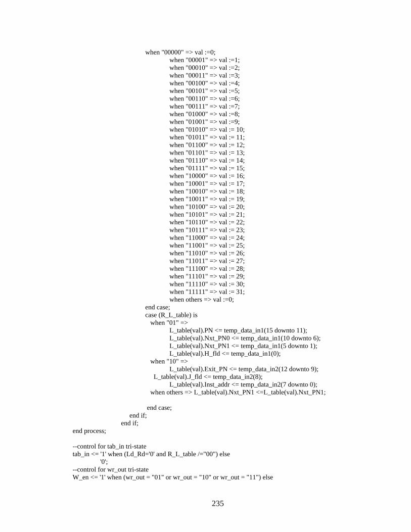
235
when "00000" => val :=0; when "00001" => val :=1; when "00010" => val :=2; when "00011" => val :=3; when "00100" => val :=4; when "00101" => val :=5; when "00110" => val :=6; when "00111" => val :=7; when "01000" => val :=8; when "01001" => val :=9; when "01010" => val := 10; when "01011" => val := 11; when "01100" => val := 12; when "01101" => val := 13; when "01110" => val := 14; when "01111" => val := 15; when "10000" => val := 16; when "10001" => val := 17; when "10010" => val := 18; when "10011" => val := 19; when "10100" => val := 20; when "10101" => val := 21; when "10110" => val := 22; when "10111" => val := 23; when "11000" => val := 24; when "11001" => val := 25; when "11010" => val := 26; when "11011" => val := 27; when "11100" => val := 28; when "11101" => val := 29; when "11110" => val := 30; when "11111" => val := 31; when others => val :=0; end case; case (R_L_table) is when "01" => L_table(val).PN <= temp_data_in1(15 downto 11); L_table(val).Nxt_PN0 <= temp_data_in1(10 downto 6); L_table(val).Nxt_PN1 <= temp_data_in1(5 downto 1); L_table(val).H_fld <= temp_data_in1(0); when "10" => L_table(val).Exit_PN <= temp_data_in2(12 downto 9); L_table(val).J_fld <= temp_data_in2(8); L_table(val).Inst_addr <= temp_data_in2(7 downto 0); when others => L_table(val).Nxt_PN1 <=L_table(val).Nxt_PN1; end case; end if; end if; end process; --control for tab_in tri-state tab_in <= '1' when (Ld_Rd='0' and R_L_table /="00") else '0'; --control for wr_out tri-state W_en <= '1' when (wr_out = "01" or wr_out = "10" or wr_out = "11") else

236
'0'; tab_in_dbg <=tab_in; send_instr: process (clk, wr_out,Snd_buf_Inst0,Snd_buf_Inst1,Snd_buf_Inst2) --send instr's to PE begin case (wr_out) is when "01" => Instr_out <= Snd_buf_Inst0; --send 1st instr --Instr_out <= "1001110000000100"; when "10" => Instr_out <= Snd_buf_Inst1; --send 2nd instr --Instr_out <= "0011000000000011"; when "11" => Instr_out <= Snd_buf_Inst2; --send other join data loc when others => Instr_out <= (others=>'0'); end case; end process; end LUT_arch; Module Name : Queue.vhd -- QUEUE.vhd used in synthesis simulation. -- Top level design for FIFO model library ieee; use ieee.std_logic_1164.all; use ieee.std_logic_unsigned.all; entity queue is -- total queue source code port ( clk, enw, rst_f,rst_r,enr,s:in std_logic; time_s: in std_logic_vector(3 downto 0); din: in std_logic_vector(17 downto 0); ram_add: in std_logic_vector(5 downto 0); prog_flag: in std_logic_vector(5 downto 0); error: inout std_logic; sign: out std_logic; ITRC: out std_logic_vector(3 downto 0); th_flag: out std_logic; count_token:inout std_logic_vector(5 downto 0); dout: out std_logic_vector(17 downto 0)); end queue; architecture queue_body of queue is component rate port ( Clk, Enw, Rst, error_full: in std_logic; time_s: in std_logic_vector(3 downto 0); sign: out std_logic; ITRC: out std_logic_vector(3 downto 0)); end component;

237
component FIFO_block_syn generic(N: integer := 18); port ( din: in std_logic_vector(N-1 downto 0); ENR: in std_logic; ENW: in std_logic; clk, Rst: in std_logic; ram_add: in std_logic_vector(5 downto 0); s:in std_logic; prog_flag: in std_logic_vector(5 downto 0); ENR_out: out std_logic; ENW_out: out std_logic; error: out std_logic; error_full: inout std_logic; th_flag: out std_logic; count_token: inout std_logic_vector(5 downto 0); wptr_out: out std_logic_vector (5 downto 0); rptr_out: out std_logic_vector (5 downto 0); dout: out std_logic_vector(N-1 downto 0)); end component; component ram port (waddr: in std_logic_vector(5 downto 0); datain: in std_logic_vector(17 downto 0); clk: in std_logic; wren: in std_logic; rden: in std_logic; raddr: in std_logic_vector(5 downto 0); dataout: out std_logic_vector(17 downto 0)); end component; signal error_full: std_logic; signal dout_ram: std_logic_vector (17 downto 0); signal dout_FIFO: std_logic_vector (17 downto 0); signal din_ram: std_logic_vector (17 downto 0); signal ENR_out, ENW_out: std_logic; signal wptr_out, rptr_out: std_logic_vector(5 downto 0); begin rate1: rate port map (Clk,Enw,Rst_r,error_full,time_s,sign,ITRC); FIFO_syn1: FIFO_block_syn port map(dout_ram,ENR,ENW,clk,Rst_f,ram_add,s,prog_flag,ENR_out, ENW_out,error,error_full,th_flag,count_token,wptr_out,rptr_out, dout_FIFO); ram1 : ram port map(wptr_out,din_ram,clk,ENW_out,ENR_out,rptr_out,dout_ram); process(s,dout_FIFO,din,dout_ram) begin case s is when '1' => din_ram <= dout_FIFO; dout <= (others => '0'); when others => din_ram <= din; dout <= dout_ram; end case; end process;

238
end queue_body; Module Name: fifo.vhd -- FIFO_block.vhd used in synthesis simulation. library ieee; use ieee.std_logic_1164.all; USE IEEE.STD_LOGIC_UNSIGNED.ALL; entity FIFO_block_syn is generic(N: integer := 18); port ( din: in std_logic_vector(N-1 downto 0); ENR: in std_logic; ENW: in std_logic; clk, Rst: in std_logic; ram_add: in std_logic_vector(5 downto 0); s:in std_logic; prog_flag: in std_logic_vector(5 downto 0); ENR_out: out std_logic; ENW_out: out std_logic; error: out std_logic; error_full: inout std_logic; th_flag: out std_logic; count_token: inout std_logic_vector(5 downto 0); wptr_out: out std_logic_vector (5 downto 0); rptr_out: out std_logic_vector (5 downto 0); dout: out std_logic_vector(N-1 downto 0)); end FIFO_block_syn; architecture FIFO_block_body of FIFO_block_syn is --------------------------------------------------------------------------------------------------------------------------------- -- -- Signals used in the Error detection unit block -- signal error_empty: std_logic; --------------------------------------------------------------------------------------------------------------------------------- -- -- Signals used in the FCU block -- signal flag_fcu1,flag_fcu2,flag_fcu3,flag_fcu4, flag_fcu5: std_logic; --------------------------------------------------------------------------------------------------------------------------------- -- -- Signals used when the pseudo-RAM function is evoked -- signal ASE1,ASE2: std_logic_vector(5 downto 0); signal dout_ASE : std_logic_vector(5 downto 0); signal RAM1,RAM2: std_logic_vector(17 downto 0); signal dout_RAM1, dout_RAM2: std_logic_vector(17 downto 0); signal din_RAM1, din_RAM2: std_logic_vector(17 downto 0); --------------------------------------------------------------------------------------------------------------------------------- signal rptr,wptr: std_logic_vector(5 downto 0); begin

239
process (wptr, rptr, s, ram_add, dout_ASE) begin case s is when '1' => rptr_out <= ram_add; wptr_out <= dout_ASE; when others => rptr_out <= rptr; wptr_out <= wptr; end case; end process; process(rst,s,flag_fcu1,flag_fcu2,flag_fcu3, flag_fcu4,flag_fcu5,ENR,ENW,error_empty,error_full) begin if rst = '1' then ENW_out <= '0'; ENR_out <= '0'; else if s = '1' then if flag_fcu1 = '0' and flag_fcu2 = '0' and flag_fcu3 = '0' and flag_fcu4 = '0' and flag_fcu5 = '0' then ENR_out <= '1'; ENW_out <='0'; elsif flag_fcu1 = '1' and flag_fcu2 = '0' and flag_fcu3 = '0' and flag_fcu4 = '0' and flag_fcu5 = '0' then ENR_out <= '1'; ENW_out <= '0'; elsif flag_fcu1 = '1' and flag_fcu2 = '1' and flag_fcu3 = '1' and flag_fcu4 = '0' and flag_fcu5 = '0' then ENR_out <= '0'; ENW_out <= '1'; elsif flag_fcu1 = '1' and flag_fcu2 = '1' and flag_fcu3 = '1' and flag_fcu4 = '1' and flag_fcu5 = '0' then ENR_out <= '0'; ENW_out <= '1'; else ENR_out <= '0'; ENW_out <= '0'; end if; else ENR_out <= ENR and (not error_empty); ENW_out <= ENW and (not error_full); end if; end if; end process; ASE_block:process(rst,s,clk) begin if rst = '1' then ASE1 <= (others => '0'); ASE2 <= (others => '0'); dout_ASE <= (others => '0'); else if s = '1' then if clk'event and clk = '1' then if flag_fcu1 = '0' and flag_fcu2 = '0' and flag_fcu3 = '0' and flag_fcu4 = '0' then ASE1 <= ram_add; elsif flag_fcu1 = '1' and flag_fcu2 = '0' and flag_fcu3 = '0' and flag_fcu4 = '0' then ASE2 <= ram_add; elsif flag_fcu1 = '1' and flag_fcu2 = '1' and flag_fcu3 = '0' and flag_fcu4 = '0' then dout_ASE <= ASE2; elsif flag_fcu1 = '1' and flag_fcu2 = '1' and flag_fcu3 = '1' and flag_fcu4 = '0' then dout_ASE <= ASE1;

240
end if; end if; end if; end if; end process; RAM_block:process(rst,clk) begin if rst = '1' then RAM1 <= (others => '0'); RAM2 <= (others =>'0'); dout<= (others => '0'); else if clk'event and clk = '1' then if s = '1' then if flag_fcu1 = '0' and flag_fcu2 = '0' and flag_fcu3 = '0' and flag_fcu4 ='0' then RAM1 <= din; elsif flag_fcu1 = '1' and flag_fcu2 = '0' and flag_fcu3 = '0' and flag_fcu4 ='0' then ram2 <= din; elsif flag_fcu1 = '1' and flag_fcu2 = '1' and flag_fcu3 = '0' and flag_fcu4 ='0' then dout <= RAM1; elsif flag_fcu1 = '1' and flag_fcu2 = '1' and flag_fcu3 = '1' and flag_fcu4 ='0' then dout <= RAM2; else RAM2 <= (others => '0'); RAM1 <= (others => '0'); end if; end if; end if; end if; end process; WAP_RAP: process (rst,clk) begin if rst = '1' then wptr <= (others => '0'); rptr <= (others => '0'); else if clk'event and clk = '1' then if s= '0' then if enw = '1' and error_full = '0' then if wptr /= "111111" then wptr <= wptr + "000001"; else wptr <= (others => '0'); end if; end if; if enr = '1' and error_empty = '0' then if rptr /= "111111" then rptr <= rptr + "000001"; else rptr <= (others => '0'); end if; end if;

241
end if; end if; end if; end process; error <= error_full or error_empty; EDU: process(rst,wptr,rptr,enw,enr,s,count_token) begin if rst = '1' then error_full <= '0'; error_empty <= '0'; else if s = '0' then if wptr = rptr and enw = '1' and enr = '0' and count_token /= "000000" then error_full <= '1'; error_empty <= '0'; elsif rptr = wptr and count_token /= "100000" and enw = '0' and enr = '1' then error_full <= '0'; error_empty <= '1'; else error_full <= '0'; error_empty <= '0'; end if; end if; end if; end process; TCU: process(rst,clk) begin if rst = '1' then count_token <= (others => '0'); else if clk'event and clk = '1' then if s = '0' then if enw = '1' and enr = '0' then if count_token /= "100000" and error_full /= '1' then count_token <= count_token + "000001"; end if; elsif enw = '0' and enr = '1' then if count_token /= "000000" and error_empty /= '1' then count_token <= count_token - "000001"; end if; end if; end if; end if; end if; end process; PTU: process(rst,s,prog_flag,count_token) begin if rst = '1' then th_flag <= '0'; else if s = '0' then if count_token >= prog_flag then th_flag <= '1'; else

242
th_flag <= '0'; end if; end if; end if; end process; FCU: process(clk,rst) begin if rst = '1' then flag_fcu1 <= '0'; flag_fcu2 <= '0'; flag_fcu3 <= '0'; flag_fcu4 <= '0'; flag_fcu5 <= '0'; else if clk'event and clk = '1' then if s = '1' then if flag_fcu1 = '0' and flag_fcu2 = '0' and flag_fcu3 = '0' and flag_fcu4 = '0' and flag_fcu5 = '0' then flag_fcu1 <= '1'; elsif flag_fcu1 = '1' and flag_fcu2 = '0' and flag_fcu3 = '0' and flag_fcu4 = '0' and flag_fcu5 = '0' then flag_fcu2 <= '1'; elsif flag_fcu1 = '1' and flag_fcu2 = '1' and flag_fcu3 = '0' and flag_fcu4 = '0' and flag_fcu5 = '0' then flag_fcu3 <= '1'; elsif flag_fcu1 = '1' and flag_fcu2 = '1' and flag_fcu3 = '1' and flag_fcu4 = '0' and flag_fcu5 = '0' then flag_fcu4 <= '1'; elsif flag_fcu1 = '1' and flag_fcu2 = '1' and flag_fcu3 = '1' and flag_fcu4 = '1' and flag_fcu5 = '0' then flag_fcu5 <= '1'; end if; else flag_fcu1 <= '0'; flag_fcu2 <= '0'; flag_fcu3 <= '0'; flag_fcu4 <= '0'; flag_fcu5 <= '0'; end if; end if; end if; end process; end FIFO_block_body; Module Name: ram.vhd -- RAM.vhd LIBRARY IEEE; USE IEEE.STD_LOGIC_1164.ALL; USE IEEE.STD_LOGIC_ARITH.ALL; USE IEEE.STD_LOGIC_UNSIGNED.ALL; USE STD.TEXTIO.ALL; entity ram is port (waddr: in std_logic_vector(5 downto 0); datain: in std_logic_vector(17 downto 0);

243
clk: in std_logic; wren: in std_logic; rden: in std_logic; raddr: in std_logic_vector(5 downto 0); dataout: out std_logic_vector(17 downto 0)); end ram; architecture ram_body of ram is constant deep: integer := 63; type fifo_array is array(deep downto 0) of std_logic_vector(17 downto 0); signal mem: fifo_array; signal waddr_int: integer range 0 to 63; signal raddr_int: integer range 0 to 63; begin waddr_int <= conv_integer(waddr); raddr_int <= conv_integer(raddr); process (clk) begin if clk'event and clk = '1' then if wren = '1' then mem(waddr_int) <= datain; end if; end if; end process; dataout <= mem(raddr_int); end ram_body; Module Name : rate.vhd -- This is the vhdl description of the rate_block library ieee; use ieee.std_logic_1164.all; use ieee.std_logic_unsigned.all; entity rate is port ( Clk, Enw, Rst, error_full: in std_logic; -- active high reset(synchronous) and write enable time_s: in std_logic_vector(3 downto 0); -- This specify the time time period one wants to -- use for calculating the difference in rate for -- 2 time period. sign: out std_logic; -- If the sign is 0 it means rate decreases and if -- it is 1 than it means the rate has increased. ITRC: out std_logic_vector(3 downto 0)); -- ITRC gives us the rate comparison of 2 time. slices end rate; architecture body_rate of rate is

244
signal time_s_temp: std_logic_vector(3 downto 0); signal count_clk : std_logic_vector(3 downto 0); -- Output from the clock counter block that tells how -- many clock cycle has passed. signal write_storeRef : std_logic; -- Control signal that acts as the write enable signal for storeRef memory -- element. signal count_t : std_logic_vector(3 downto 0); -- Output from the token_counter block that gives -- information on how many control token is written into the -- memory array within a time slice. signal storeRef : std_logic_vector(3 downto 0); -- Output of the store_ref_rate block and is used as the -- reference to count the build up rate. signal storeComp,fill_flag : std_logic_vector(3 downto 0); -- Output of the store_comp_rate block and is -- used as the comparator value to count the -- ITRC. signal mem_stack: std_logic_vector(7 downto 0); signal last : std_logic; signal time_s_temp_lessOne : integer range 0 to 8; begin CCU:process(clk,rst,time_s) -- This section describes the clock counter unit block begin if rst = '1' then time_s_temp <= time_s; -- store the desired time period count_clk <= (others => '0'); write_storeRef <= '0'; case time_s is when "0000" => time_s_temp_lessOne <= 0; when "0001" => time_s_temp_lessOne <= 0; when "0010" => time_s_temp_lessOne <= 0; when "0011" => time_s_temp_lessOne <= 1; when "0100" => time_s_temp_lessOne <= 2; when "0101" => time_s_temp_lessOne <= 3; when "0110" => time_s_temp_lessOne <= 4; when "0111" => time_s_temp_lessOne <= 5; when "1000" => time_s_temp_lessOne <= 6; when others => time_s_temp_lessOne <= 0; end case; elsif (Clk'event and Clk = '1') then if error_full = '0' then if (count_clk = time_s_temp) then count_clk <= "0001"; else if count_clk /= "1000" then count_clk <= count_clk + "0001"; end if;
245
end if; if (count_clk = (time_s_temp -"0001")) then write_storeRef <= '1'; else write_storeRef <= '0'; end if; end if; end if; end process; WTCU: process(clk,rst) -- This section describes the write token counter unit block begin if rst = '1' then count_t <= (others => '0'); elsif clk'event and clk = '1' then if error_full = '0' then if count_clk = time_s_temp then if enw = '1' then count_t <= "0001"; else count_t <= "0000"; end if; else if enw = '1' then if count_t /= "1000" then count_t <= count_t + "0001"; end if; end if; end if; end if; end if; end process; SE2:process(clk,rst) -- This section describes the SE1 block that is used to store the RITB. begin if rst = '1' then storeRef <= (others => '0'); elsif clk'event and clk = '1' then if error_full = '0' then if write_storeRef = '1' then storeRef <= count_t; end if; end if; end if; end process; SE3: process(clk,rst) -- This section describes the SE3 block that is used to -- store and determine the NITB. begin if rst = '1' then storeComp <= (others => '0'); fill_flag <= (others => '0'); elsif clk'event and clk = '1' then if error_full = '0' then if fill_flag /= time_s_temp then

246
fill_flag <= fill_flag + "0001"; if enw = '1' and last = '0' then storeComp <= storeComp + "0001"; end if; else if enw = '1' and storeComp /= time_s_temp and last = '0' then storeComp <= storeComp + "0001"; elsif enw = '0' and storeComp /= "0000" and last = '1' then storeComp <= storeComp - "0001"; end if; end if; end if; end if; end process; AU: process (storeComp, storeRef, Rst, error_full) -- This section describes the arithetic unit block that -- is used to count the input token buildup begin if Rst = '1' then sign <= '0'; ITRC <= (others => '0'); else if error_full = '0' then if storeRef > storeComp then ITRC <= storeRef - storeComp; sign <= '0'; elsif storeRef = storeComp then ITRC <= (others => '0'); sign <= '0'; else ITRC <= storeComp - storeRef; sign <= '1'; end if; end if; end if; end process; process(clk,rst) begin if rst = '1' then last <= '0'; mem_stack <= (others => '0'); elsif clk'event and clk = '1' then if error_full = '0' then last <= mem_stack(time_s_temp_lessOne); if enw = '1' then mem_stack <= mem_stack(6 downto 0) & '1'; else mem_stack <= mem_stack(6 downto 0) & '0'; end if; end if; end if; end process; end body_rate; Module Name: divpe.vhd -- Code for Divider Processor for HDFCA project

247
-- File: divpe.vhd -- synopsys translate_off Library XilinxCoreLib; -- synopsys translate_on --The IEEE standard 1164 package, declares std_logic, rising_edge(), etc. library IEEE; use IEEE.std_logic_1164.all; use IEEE.std_logic_arith.all; use IEEE.std_logic_unsigned.all; entity Divpe is port (Cntrlr_bus : in std_logic_vector(15 downto 0); Snd_I : out std_logic; clk : in std_logic; rst : in std_logic; Instr_rdy : in std_logic; Fin : out std_logic; Data_bus : inout std_logic_vector(15 downto 0); Bus_req : out std_logic; Bus_gnt : in std_logic; Addr : out std_logic_vector(6 downto 0); R_W : buffer std_logic; --R_W : inout std_logic; loc_bus_dbug : out std_logic_vector(7 downto 0); Iaddr_bus_dbug : out std_logic_vector(7 downto 0); Iaddr_dbug : out std_logic_vector(7 downto 0); R2_out_dbug : out std_logic_vector( 7 downto 0); Imem_bus_dbug : out std_logic_vector(15 downto 0 ) --LR2_dbug : out std_logic ); end Divpe; architecture dpe of Divpe is ---------------------------------------------------------------------- -- This file was created by the Xilinx CORE Generator tool, and -- -- is (c) Xilinx, Inc. 1998, 1999. No part of this file may be -- -- transmitted to any third party (other than intended by Xilinx) -- -- or used without a Xilinx programmable or hardwire device without -- -- Xilinx's prior written permission. -- ---------------------------------------------------------------------- component div1 port ( dividend: IN std_logic_VECTOR(15 downto 0); divisor: IN std_logic_VECTOR(15 downto 0); quot: OUT std_logic_VECTOR(15 downto 0); remd: OUT std_logic_VECTOR(15 downto 0); c: IN std_logic); end component;

248
---------------------------------------------------------------------- -- This file was created by the Xilinx CORE Generator tool, and -- -- is (c) Xilinx, Inc. 1998, 1999. No part of this file may be -- -- transmitted to any third party (other than intended by Xilinx) -- -- or used without a Xilinx programmable or hardwire device without -- -- Xilinx's prior written permission. -- ---------------------------------------------------------------------- component div_imem port ( addr: IN std_logic_VECTOR(3 downto 0); clk: IN std_logic; din: IN std_logic_VECTOR(15 downto 0); dout: OUT std_logic_VECTOR(15 downto 0); we: IN std_logic); end component; component add_subber8 port ( A: IN std_logic_VECTOR(7 downto 0); B: IN std_logic_VECTOR(7 downto 0); C_IN: IN std_logic; C_OUT: OUT std_logic; ADD_SUB: IN std_logic; Q_OUT: OUT std_logic_VECTOR(7 downto 0)); end component; signal Imem_bus, R0_out, R1_out, Inst_in, Inst_out : std_logic_vector(15 downto 0); signal R2_out, Data_loc1, Data_loc2 : std_logic_vector(7 downto 0); signal s2, s1, s0, s3 ,s4, s5, s6, s7 : std_logic; signal Div_out, mux2_out, adder_out : std_logic_vector(7 downto 0); signal mux1_out, result : std_logic_vector(15 downto 0); signal div_en, ld_d1, ld_d2, ld_iaddr : std_logic; signal loc_bus, Iaddr, Iaddr_bus : std_logic_vector(7 downto 0); constant GoDiv : std_logic_vector(7 downto 0) := "11111111"; constant StoreDL : std_logic_vector(7 downto 0) := "10001000"; type OP_state is (reset,Getop,O1,O2,O3,O4,O5,O5A,O5B,O5C,O6,O7,O8,O9,O10); signal OP : OP_state; signal LR2, LR1, Ci, LR0, R2_rst, ld_rslt, I_R_W : std_logic; signal qout_out, remd_out, rem_rslt : std_logic_vector(15 downto 0); signal mux5_out, mux6_out, MUX4_OUT : std_logic_vector(7 downto 0); signal delay : std_logic_vector(19 downto 0); signal one, zero : std_logic; signal test :string (1 to 10); begin one <= '1'; zero <= '0'; -- added for dbugging loc_bus_dbug <= loc_bus; Iaddr_bus_dbug <= Iaddr_bus; Iaddr_dbug <= Iaddr; R2_out_dbug <= R2_out; Imem_bus_dbug <= Imem_bus;

249
--LR2_dbug <=LR2; ---- ADD5 : add_subber8 port map ( A =>R2_out, B =>mux2_out, C_IN => Ci, C_OUT => open, ADD_SUB =>one, Q_OUT =>adder_out); D2 : div1 port map (dividend => R0_out, divisor => R1_out, quot => qout_out, remd => remd_out, c => clk); mux2_out <= data_loc2 when (s3='0' and s2='0') else data_loc1 when (s3='0' and s2='1') else Iaddr when (s3='1' and s2='0') else (others=> '0'); mux1_out <= Data_bus when s1='0' else Imem_bus; Addr <= Data_loc2(6 downto 0) when s0='0' else data_loc1(6 downto 0); mux4_out <= Iaddr_bus when s4='0' else adder_out; mux5_out <= loc_bus when s5 = '0' else adder_out; mux6_out <= loc_bus when s6 = '0' else adder_out; DIM1 : div_imem port map (addr => Iaddr(3 downto 0), clk => clk, din => Inst_in, dout => Inst_out, we => I_R_W); Imem_bus <= Inst_out when I_R_W = '0' else (others=>'Z'); Inst_in <= Imem_bus when I_R_W = '1' else (others=>'0'); Data_bus <= result when (R_W = '1' and S7 = '0') else rem_rslt when (R_W = '1' and S7 = '1') else (others=>'Z'); control: process(clk, instr_rdy, bus_gnt, cntrlr_bus, rst, delay, data_loc2,Op) variable load_delay, ld_del2, del : boolean; begin if rst = '1' then OP <= reset; elsif (clk'event and clk = '1') then if Op = reset then test <= "StateReset"; snd_i <= '1'; del := false; fin <= '1'; ld_del2 := false; bus_req <= '0'; I_R_W <= '0';

250
r_w <= '0'; LR0 <= '0'; s4 <= '0'; s1 <= '0'; s2 <= '0'; s3 <= '0'; s0 <= '1'; s5 <= '0'; s6 <= '0'; s7 <= '0'; Ci <= '0'; LR2 <= '0'; LR1 <= '0'; LD_D1 <= '0'; LD_D2 <= '0'; r2_rst <= '1'; load_delay := false; ld_rslt <= '0'; ld_Iaddr<= '0'; delay <= "00000000000000000001"; Op <= GetOp; elsif Op = GetOp then --ld data loc 1 r2_rst <= '0'; LD_D2 <= '0'; LR2 <= '0'; LR1 <= '0'; bus_req <= '0'; ld_rslt <= '0'; ld_Iaddr<= '0'; if instr_rdy = '1' then loc_bus <= Cntrlr_bus(7 downto 0); LD_D1 <= '1'; fin <= '0'; s5 <= '0'; Snd_i <= '1'; Op <= O1; else OP <= GetOp; end if; elsif Op = O1 then LD_D1 <= '0'; r2_rst <= '0'; LR2 <= '0'; LR1 <= '0'; bus_req <= '0'; ld_rslt <= '0'; if (instr_rdy = '1' or load_delay = true) then if cntrlr_bus(15 downto 8) = StoreDL then --ld dl2 loc_bus <= cntrlr_bus(7 downto 0); LD_D2 <= '1'; ld_Iaddr<= '0'; fin <= '0'; s6 <= '0'; snd_i <='1'; Op <= O1; elsif cntrlr_bus(15 downto 8) = GoDiv then --start div ops if (load_delay = false) then Iaddr_bus <= cntrlr_bus(7 downto 0); --ld instr loc LD_D2 <= '0'; s4 <= '0'; Ld_Iaddr <= '1'; Snd_I <= '0'; load_delay := true; Op <= O1; elsif (load_delay = true) then Ld_Iaddr <= '0'; Op <= O2; load_delay := false; end if; end if; else Op <= O1; end if; elsif Op = O2 then --ld R2 with dl1 offset r2_rst <= '0'; LD_D2 <= '0'; --from Imem LR1 <= '0'; ld_d1 <= '0';

251
bus_req <= '0'; ld_rslt <= '0'; ld_Iaddr <= '0'; I_R_W <= '0'; LR2 <= '1'; Op <= O3; elsif Op = O3 then --add offset to dl1 str in dl1 LD_D2 <= '0'; -- changes for dbugging --LR2 <= '1'; LR2 <= '0'; LR1 <= '0'; bus_req <= '0'; ld_rslt <= '0'; ld_Iaddr<= '0'; Ci <= '0'; LR2 <= '0'; LD_D1 <= '1'; S5 <= '1'; s2 <= '1'; s3 <= '0'; Op <= O4; r2_rst <= '1'; elsif Op = O4 then --Inc Iaddr if (ld_del2 = false) then LD_D2 <= '0'; LR2 <= '0'; LR1 <= '0'; bus_req <= '0'; ld_rslt <= '0'; LD_D1 <= '0'; r2_rst <= '0'; s2 <= '0'; s3 <= '1'; S4<='1'; ci <= '1'; ld_Iaddr <= '1'; Op <= O4; ld_del2 := true; elsif (ld_del2 = true) then ld_Iaddr <= '0'; Op <= O5; ld_del2 := false; end if; elsif Op = O5 then --Check for 2nd dl r2_rst <= '0'; LD_D2 <= '0'; bus_req <= '0'; ld_d1 <= '0'; ld_rslt <= '0'; ld_Iaddr <= '0'; if data_loc2 = "00000000" then --get divisor from IMEM I_R_W <= '0'; lr0 <= '0'; --put in R1 S1 <= '1'; lr1 <= '1'; Op <= O6; else --get data from DMEM I_R_W <= '0'; lr0 <= '0'; --get offset to Dl2 lr2 <='1'; Op <= O5a; lr1<='0'; end if; elsif Op = O5a then --add offset to Dl2 r2_rst <= '0'; LR1 <= '0'; bus_req <= '0'; ld_d1 <= '0'; ld_rslt <= '0'; ld_Iaddr<= '0'; lr2 <= '0'; s2 <= '0'; s3 <= '0'; ci <= '0'; s6 <= '1'; LD_D2 <= '1'; Op <= O5b; elsif Op = O5b then

252
test <= "State O5b "; r2_rst <= '0'; LR2 <= '0'; LR1 <= '0'; ld_d1 <= '0'; ld_rslt <= '0'; ld_Iaddr<= '0'; LD_D2 <= '0'; s0 <= '0'; bus_req <= '1'; R_w <= '0'; Op <= O5c; s1 <= '0'; elsif Op = O5c then --ld R1 with divisor test <= "State O5c "; r2_rst <= '0'; LD_D2 <= '0'; --from DMEM LR2 <= '0'; s1 <= '0'; ld_d1 <= '0'; ld_rslt <= '0'; ld_Iaddr<= '0'; if bus_gnt = '1' then lr1 <= '1'; Op <= O6; else LR1 <= '0'; Op <= O5c; end if; elsif Op = O6 then --ld R0 with dividend test <= "State O6 "; r2_rst <= '0'; LD_D2 <= '0'; LR2 <= '0'; LR1 <= '0'; ld_d1 <= '0'; ld_rslt <= '0'; ld_Iaddr<= '0'; s0<= '1'; R_w <= '0'; bus_req <= '1'; Op <= O7; elsif Op = O7 then r2_rst <= '0'; LD_D2 <= '0'; LR2 <= '0'; LR1 <= '0'; ld_d1 <= '0'; ld_rslt <= '0'; ld_Iaddr<= '0'; if bus_gnt = '1' then lr0 <= '1'; Op <= O8; else lr0 <= '0'; OP <= O7; end if; elsif Op = O8 then --wait for result 20 CC's LD_D2 <= '0'; LR2 <= '0'; LR1 <= '0'; bus_req <= '0'; ld_d1 <= '0'; ld_Iaddr<= '0';lr0 <= '0'; bus_req <= '0'; r2_Rst <= '1'; if delay = "10000000000000000000" then Ld_rslt <= '1'; Op <= O9; else

253
delay <= delay(18 downto 0)&'0'; ld_rslt <= '0'; Op <= O8; end if; elsif Op = O9 then test <= "State O9 "; r2_rst <= '0'; LR2 <= '0'; LR1 <= '0'; ld_rslt <= '0'; ld_Iaddr<= '0'; r2_Rst <= '0'; R_W <= '1'; if data_loc2 = "00000000" then --use DL1 for store S0<='1'; ld_d2 <= '0'; else --use DL2 for store S0 <= '0'; ld_d1 <= '0'; end if; Bus_req <= '1'; Op <= O10; elsif Op = O10 then test <= "State O10 "; r2_rst <= '0'; LD_D2 <= '0'; LR2 <= '0'; LR1 <= '0'; ld_d1 <= '0'; S7 <= '0'; ld_rslt <= '0'; ld_Iaddr<= '0'; if bus_gnt = '1' then --Store Quotient in mem fin <= '1'; bus_req <= '0'; Op <= reset; else Op <= O10; end if; end if; end if; end process; reg2 : process (clk, Imem_bus, R2_rst, Lr2) begin if clk'event and clk='1' then if R2_rst = '1' then R2_out <= (others=>'0'); elsif lr2 = '1' then R2_out <= Imem_bus(7 downto 0); else R2_out <= R2_out; end if; end if; end process; reg_dl1: process (clk, mux5_out, rst, LD_D1) begin if rst ='1' then data_loc1 <= (others=>'0'); elsif clk'event and clk='1' then

254
if LD_D1 = '1' then data_loc1 <= mux5_out; else data_loc1 <= data_loc1; end if; end if; end process; reg_dl2: process (clk, mux6_out, rst, LD_D2) begin if rst ='1' then data_loc2 <= (others=>'0'); elsif clk'event and clk='1' then if LD_D2 = '1' then data_loc2 <= mux6_out; else data_loc2 <= data_loc2; end if; end if; end process; reg_R0: process (clk, data_bus, rst, lR0) begin if rst ='1' then R0_out <= (others=>'0'); elsif clk'event and clk='1' then if lR0 = '1' then R0_out <= data_bus; else R0_out <= R0_out; end if; end if; end process; reg_R1: process (clk, mux1_out, rst, lR1) begin if rst ='1' then R1_out <= (others=>'0'); elsif clk'event and clk='1' then if lR1 = '1' then R1_out <= mux1_out; else R1_out <= R1_out; end if; end if; end process; reg_Iaddr: process (clk, mux4_out, rst, ld_Iaddr) begin if rst ='1' then Iaddr <= (others=>'0'); elsif clk'event and clk='1' then if ld_Iaddr = '1' then Iaddr <= mux4_out; else Iaddr <= Iaddr;

255
end if; end if; end process; reg_Rslt: process (clk, qout_out, remd_out, rst, ld_Rslt) begin if rst ='1' then result <= (others=>'0'); rem_rslt <= (others=>'0'); elsif clk'event and clk='1' then if ld_Rslt = '1' then result <= qout_out; rem_rslt <= remd_out; else result <= result; rem_rslt <= rem_rslt; end if; end if; end process; end architecture; Module Name : addsub8_synthable.vhd LIBRARY IEEE; USE IEEE.std_logic_1164.ALL; USE IEEE.std_logic_unsigned.ALL; --use ieee.std_logic_arith.all; ENTITY add_subber8 IS PORT( A: IN std_logic_vector(7 DOWNTO 0); B: IN std_logic_vector(7 DOWNTO 0); C_IN: IN std_logic; C_OUT: OUT std_logic; ADD_SUB: IN std_logic; Q_OUT: OUT std_logic_vector(7 DOWNTO 0)); END add_subber8; ARCHITECTURE sim OF add_subber8 IS SIGNAL S: std_logic_vector(7 DOWNTO 0); SIGNAL S1: std_logic_vector(7 DOWNTO 0); SIGNAL AA: std_logic_vector(7 DOWNTO 0); SIGNAL C: std_logic_vector(8 DOWNTO 0); SIGNAL T: std_logic_vector(7 DOWNTO 0); BEGIN Q_OUT<=S; PROCESS(A,B,C_IN,ADD_SUB,C,T,AA,S1,S) begin if ADD_SUB='1' THEN C(0)<= C_IN; for i in 0 to 7 loop S(i) <= A(i) xor B(i) xor C(i);

256
C(i+1)<= (A(i) and B(i)) or (A(i) and C(i)) or (B(i) and C(i)); end loop; C_OUT <= C(8); else T<=NOT (B+C_IN); AA<=A+1; C(0) <= C_in; for i in 0 to 7 loop S1(i) <= AA(i) xor T(i) xor C(i); C(i+1)<= (AA(i) and T(i)) or (AA(i) and C(i)) or (T(i) and C(i)); end loop; --C_OUT <= NOT C(8); C_OUT <= C(8); if C(8) = '0' then --if s1(7) = '1' and A(7) = '0' then s <= (not s1) +1; else s <= s1; end if; end if; end process; END sim; Module Name: div1.xco ( Xilinx IP Core) -------------------------------------------------------------------------------- -- This file is owned and controlled by Xilinx and must be used -- -- solely for design, simulation, implementation and creation of -- -- design files limited to Xilinx devices or technologies. Use -- -- with non-Xilinx devices or technologies is expressly prohibited -- -- and immediately terminates your license. -- -- -- -- XILINX IS PROVIDING THIS DESIGN, CODE, OR INFORMATION "AS IS" -- -- SOLELY FOR USE IN DEVELOPING PROGRAMS AND SOLUTIONS FOR -- -- XILINX DEVICES. BY PROVIDING THIS DESIGN, CODE, OR INFORMATION -- -- AS ONE POSSIBLE IMPLEMENTATION OF THIS FEATURE, APPLICATION -- -- OR STANDARD, XILINX IS MAKING NO REPRESENTATION THAT THIS -- -- IMPLEMENTATION IS FREE FROM ANY CLAIMS OF INFRINGEMENT, -- -- AND YOU ARE RESPONSIBLE FOR OBTAINING ANY RIGHTS YOU MAY REQUIRE -- -- FOR YOUR IMPLEMENTATION. XILINX EXPRESSLY DISCLAIMS ANY -- -- WARRANTY WHATSOEVER WITH RESPECT TO THE ADEQUACY OF THE -- -- IMPLEMENTATION, INCLUDING BUT NOT LIMITED TO ANY WARRANTIES OR -- -- REPRESENTATIONS THAT THIS IMPLEMENTATION IS FREE FROM CLAIMS OF -- -- INFRINGEMENT, IMPLIED WARRANTIES OF MERCHANTABILITY AND FITNESS -- -- FOR A PARTICULAR PURPOSE. -- -- -- -- Xilinx products are not intended for use in life support -- -- appliances, devices, or systems. Use in such applications are -- -- expressly prohibited. -- -- -- -- (c) Copyright 1995-2003 Xilinx, Inc. -- -- All rights reserved. -- -------------------------------------------------------------------------------- -- You must compile the wrapper file div1.vhd when simulating -- the core, div1. When compiling the wrapper file, be sure to

257
-- reference the XilinxCoreLib VHDL simulation library. For detailed -- instructions, please refer to the "CORE Generator Guide". -- The synopsys directives "translate_off/translate_on" specified -- below are supported by XST, FPGA Compiler II, Mentor Graphics and Synplicity -- synthesis tools. Ensure they are correct for your synthesis tool(s). -- synopsys translate_off LIBRARY ieee; USE ieee.std_logic_1164.ALL; Library XilinxCoreLib; ENTITY div1 IS port ( dividend: IN std_logic_VECTOR(15 downto 0); divisor: IN std_logic_VECTOR(15 downto 0); quot: OUT std_logic_VECTOR(15 downto 0); remd: OUT std_logic_VECTOR(15 downto 0); c: IN std_logic); END div1; ARCHITECTURE div1_a OF div1 IS component wrapped_div1 port ( dividend: IN std_logic_VECTOR(15 downto 0); divisor: IN std_logic_VECTOR(15 downto 0); quot: OUT std_logic_VECTOR(15 downto 0); remd: OUT std_logic_VECTOR(15 downto 0); c: IN std_logic); end component; -- Configuration specification for all : wrapped_div1 use entity XilinxCoreLib.dividervht(behavioral) generic map( dividend_width => 16, signed_b => 0, fractional_b => 0, divisor_width => 16, fractional_width => 16, divclk_sel => 1); BEGIN U0 : wrapped_div1 port map ( dividend => dividend, divisor => divisor, quot => quot, remd => remd, c => c); END div1_a; -- synopsys translate_on Module Name : div_imem.xco (Xilinx IP Core)

258
-------------------------------------------------------------------------------- -- This file is owned and controlled by Xilinx and must be used -- -- solely for design, simulation, implementation and creation of -- -- design files limited to Xilinx devices or technologies. Use -- -- with non-Xilinx devices or technologies is expressly prohibited -- -- and immediately terminates your license. -- -- -- -- XILINX IS PROVIDING THIS DESIGN, CODE, OR INFORMATION "AS IS" -- -- SOLELY FOR USE IN DEVELOPING PROGRAMS AND SOLUTIONS FOR -- -- XILINX DEVICES. BY PROVIDING THIS DESIGN, CODE, OR INFORMATION -- -- AS ONE POSSIBLE IMPLEMENTATION OF THIS FEATURE, APPLICATION -- -- OR STANDARD, XILINX IS MAKING NO REPRESENTATION THAT THIS -- -- IMPLEMENTATION IS FREE FROM ANY CLAIMS OF INFRINGEMENT, -- -- AND YOU ARE RESPONSIBLE FOR OBTAINING ANY RIGHTS YOU MAY REQUIRE -- -- FOR YOUR IMPLEMENTATION. XILINX EXPRESSLY DISCLAIMS ANY -- -- WARRANTY WHATSOEVER WITH RESPECT TO THE ADEQUACY OF THE -- -- IMPLEMENTATION, INCLUDING BUT NOT LIMITED TO ANY WARRANTIES OR -- -- REPRESENTATIONS THAT THIS IMPLEMENTATION IS FREE FROM CLAIMS OF -- -- INFRINGEMENT, IMPLIED WARRANTIES OF MERCHANTABILITY AND FITNESS -- -- FOR A PARTICULAR PURPOSE. -- -- -- -- Xilinx products are not intended for use in life support -- -- appliances, devices, or systems. Use in such applications are -- -- expressly prohibited. -- -- -- -- (c) Copyright 1995-2002 Xilinx, Inc. -- -- All rights reserved. -- -------------------------------------------------------------------------------- -- You must compile the wrapper file div_imem.vhd when simulating -- the core, div_imem. When compiling the wrapper file, be sure to -- reference the XilinxCoreLib VHDL simulation library. For detailed -- instructions, please refer to the "Coregen Users Guide". -- The synopsys directives "translate_off/translate_on" specified -- below are supported by XST, FPGA Express, Exemplar and Synplicity -- synthesis tools. Ensure they are correct for your synthesis tool(s). -- synopsys translate_off LIBRARY ieee; USE ieee.std_logic_1164.ALL; Library XilinxCoreLib; ENTITY div_imem IS port ( addr: IN std_logic_VECTOR(3 downto 0); clk: IN std_logic; din: IN std_logic_VECTOR(15 downto 0); dout: OUT std_logic_VECTOR(15 downto 0); we: IN std_logic); END div_imem; ARCHITECTURE div_imem_a OF div_imem IS component wrapped_div_imem port ( addr: IN std_logic_VECTOR(3 downto 0);

259
clk: IN std_logic; din: IN std_logic_VECTOR(15 downto 0); dout: OUT std_logic_VECTOR(15 downto 0); we: IN std_logic); end component; -- Configuration specification for all : wrapped_div_imem use entity XilinxCoreLib.blkmemsp_v5_0(behavioral) generic map( c_sinit_value => "0", c_reg_inputs => 0, c_yclk_is_rising => 1, c_has_en => 0, c_ysinit_is_high => 1, c_ywe_is_high => 1, c_ytop_addr => "1024", c_yprimitive_type => "4kx1", c_yhierarchy => "hierarchy1", c_has_rdy => 0, c_has_limit_data_pitch => 0, c_write_mode => 0, c_width => 16, c_yuse_single_primitive => 0, c_has_nd => 0, c_enable_rlocs => 0, c_has_we => 1, c_has_rfd => 0, c_has_din => 1, c_ybottom_addr => "0", c_pipe_stages => 0, c_yen_is_high => 1, c_depth => 16, c_has_default_data => 0, c_limit_data_pitch => 8, c_has_sinit => 0, c_mem_init_file => "div_imem.mif", c_default_data => "0", c_ymake_bmm => 0, c_addr_width => 4); BEGIN U0 : wrapped_div_imem port map ( addr => addr, clk => clk, din => din, dout => dout, we => we); END div_imem_a; -- synopsys translate_on Module Name : ic_hdca_gate.vhd library IEEE; use IEEE.STD_LOGIC_1164.ALL;

260
use IEEE.STD_LOGIC_ARITH.ALL; use IEEE.STD_LOGIC_UNSIGNED.ALL; -- Uncomment the following lines to use the declarations that are -- provided for instantiating Xilinx primitive components. --library UNISIM; --use UNISIM.VComponents.all; entity gate_ic_a is Port ( clk: in std_logic ; rst: in std_logic ; ctrl: in std_logic_vector(3 downto 0) ; qdep: in std_logic_vector(19 downto 0) ; addr_bus: in std_logic_vector(27 downto 0) ; data_in0,data_in1,data_in2,data_in3 : in std_logic_vector(15 downto 0) ; rw: in std_logic_vector(3 downto 0) ; flag: out std_logic_vector(3 downto 0) ; data_out0,data_out1,data_out2,data_out3: out std_logic_vector(15 downto 0) -- f_s_out0,f_s_out1,f_s_out2,f_s_out3 : out std_logic_vector(3 downto 0); -- dco_out0,dco_out1,dco_out2,dco_out3 : out std_logic_vector(3 downto 0) ); end gate_ic_a; architecture gate_level of gate_ic_a is -- component listing component Dec_ic_a is port(dec_out : out std_logic_vector( 3 downto 0); ctrl_dec : in std_logic; addr_blk : in std_logic_vector(1 downto 0) ); end component; component prl_behav is Port (clk,rst : in std_logic; d0,d1,d2,d3 : in std_logic; q0,q1,q2,q3 : in std_logic_vector( 4 downto 0); sub_flg : out std_logic_vector ( 3 downto 0) ); end component; -- memory array ---- type mem_array is array ( 127 downto 0) of std_logic_vector(15 downto 0); --signal list signal d_sig0,d_sig1,d_sig2,d_sig3 : std_logic_vector(3 downto 0); signal flg_sig0,flg_sig1,flg_sig2,flg_sig3: std_logic_vector( 3 downto 0); signal memory : mem_array; signal flag_decide0,flag_decide1,flag_decide2,flag_decide3: std_logic_vector(3 downto 0); signal flag_wire: std_logic_vector(3 downto 0); -- make qdep as signal --signal qd00,qd01,qd02,qd03 : std_logic_vector( 3 downto 0);

261
-- signal list end here begin -- signals to ports if any --f_s_out0 <= flg_sig0; --f_s_out1 <= flg_sig1; --f_s_out2 <= flg_sig2; --f_s_out3 <= flg_sig3; --dco_out0 <= d_sig0; --dco_out1 <= d_sig1; --dco_out2 <= d_sig2; --dco_out3 <= d_sig3; flag <= flag_wire; flag_decide0<= flg_sig0(0)&flg_sig1(0)&flg_sig2(0)&flg_sig3(0); flag_decide1<= flg_sig0(1)&flg_sig1(1)&flg_sig2(1)&flg_sig3(1); flag_decide2<= flg_sig0(2)&flg_sig1(2)&flg_sig2(2)&flg_sig3(2); flag_decide3<= flg_sig0(3)&flg_sig1(3)&flg_sig2(3)&flg_sig3(3); -- port mapping -- decoder instantiated 4 times DEC0 : Dec_ic_a port map(dec_out => d_sig0, ctrl_dec => ctrl(0), addr_blk => addr_bus(6 downto 5) ); DEC1 : Dec_ic_a port map(dec_out => d_sig1, ctrl_dec => ctrl(1), addr_blk => addr_bus(13 downto 12) ); DEC2 : Dec_ic_a port map(dec_out => d_sig2, ctrl_dec => ctrl(2), addr_blk => addr_bus(20 downto 19) ); DEC3 : Dec_ic_a port map(dec_out => d_sig3, ctrl_dec => ctrl(3), addr_blk => addr_bus(27 downto 26) ); -- decoder instantiation ends ---- -- pr logic instantiation 4 times ---- PRL_LOGIC0 : prl_behav port map( clk => clk, rst => rst, d0 => d_sig0(0),

262
d1 => d_sig1(0), d2 => d_sig2(0), d3 => d_sig3(0), q0 => qdep(4 downto 0), q1 => qdep(9 downto 5), q2 => qdep(14 downto 10), q3 => qdep(19 downto 15), sub_flg => flg_sig0 ); PRL_LOGIC1 : prl_behav port map( clk => clk, rst => rst, d0 => d_sig0(1), d1 => d_sig1(1), d2 => d_sig2(1), d3 => d_sig3(1), q0 => qdep( 4 downto 0), q1 => qdep(9 downto 5), q2 => qdep(14 downto 10), q3 => qdep(19 downto 15), sub_flg => flg_sig1 ); PRL_LOGIC2 : prl_behav port map( clk => clk, rst => rst, d0 => d_sig0(2), d1 => d_sig1(2), d2 => d_sig2(2), d3 => d_sig3(2), q0 => qdep(4 downto 0), q1 => qdep(9 downto 5), q2 => qdep(14 downto 10), q3 => qdep(19 downto 15), sub_flg => flg_sig2 ); PRL_LOGIC3 : prl_behav port map( clk => clk, rst => rst, d0 => d_sig0(3), d1 => d_sig1(3), d2 => d_sig2(3), d3 => d_sig3(3), q0 => qdep(4 downto 0), q1 => qdep(9 downto 5), q2 => qdep(14 downto 10), q3 => qdep(19 downto 15), sub_flg => flg_sig3 ); -- extra logic to be added since all the prl_blks give output flag value ... -- there would be conflict as to what the final value is

263
-- try and include it in a process ... so that flag value changes in accordance with the -- clk .. flag_assign : process (clk,rst,flag_decide0,flag_decide1,flag_decide2,flag_decide3) begin if(rst ='1') then flag_wire <= "0000"; elsif (clk'event and clk ='0') then case flag_decide0 is when "0000" => flag_wire(0) <= '0'; when others => flag_wire(0) <= '1'; end case; case flag_decide1 is when "0000" => flag_wire(1) <= '0'; when others => flag_wire(1) <= '1'; end case; case flag_decide2 is when "0000" => flag_wire(2) <= '0'; when others => flag_wire(2) <= '1'; end case; case flag_decide3 is when "0000" => flag_wire(3) <= '0'; when others => flag_wire(3) <= '1'; end case; end if; end process flag_assign; -- end of extra logic added ---------- -- write about r_w logic,shall come along with flag thing ---- data_transfer : process(rst,data_in0,data_in1,data_in2,data_in3,flag_wire,rw,clk) begin if (rst ='1') then --flag <= "0000"; data_out0 <=x"0000"; data_out1 <=x"0000"; data_out2 <=x"0000"; data_out3 <=x"0000"; -- making the memory array all zeroes MEM : for i in 0 to 127 loop memory(i)<=x"0000";

264
end loop MEM; else if (clk'event and clk ='1') then if (flag_wire(0) ='1')then if (rw(0) ='1') then memory(conv_integer(addr_bus( 6 downto 0))) <= data_in0; elsif (rw(0)='0')then data_out0 <= memory(conv_integer(addr_bus( 6 downto 0))); end if; end if; if (flag_wire(1) ='1') then if (rw(1) ='1') then memory(conv_integer(addr_bus( 13 downto 7))) <= data_in1; --data_out1 <=(others =>'Z'); --commented later else data_out1 <= memory(conv_integer(addr_bus( 13 downto 7))); end if; end if; if (flag_wire(2) ='1') then if (rw(2) ='1') then memory(conv_integer(addr_bus( 20 downto 14))) <= data_in2; --data_out2 <=(others =>'Z'); else data_out2 <= memory(conv_integer(addr_bus(20 downto 14))); end if; end if; if (flag_wire(3) ='1') then if (rw(3) ='1') then memory(conv_integer(addr_bus( 27 downto 21))) <= data_in3; --data_out3 <=(others =>'Z'); else data_out3 <= memory(conv_integer(addr_bus(27 downto 21))); end if; end if; end if; end if; end process data_transfer; end gate_level; Module Name : dec_ic_a.vhd library IEEE; use IEEE.STD_LOGIC_1164.ALL; use IEEE.STD_LOGIC_ARITH.ALL; use IEEE.STD_LOGIC_UNSIGNED.ALL; -- Uncomment the following lines to use the declarations that are -- provided for instantiating Xilinx primitive components.

265
--library UNISIM; --use UNISIM.VComponents.all; entity dec_ic_a is Port (dec_out : out std_logic_vector( 3 downto 0); ctrl_dec : in std_logic; addr_blk : in std_logic_vector(1 downto 0) ); end dec_ic_a; architecture Behavioral of dec_ic_a is signal ctrl_bar,addr1_bar,addr0_bar : std_logic; begin ctrl_bar <= not ctrl_dec; addr1_bar <= not addr_blk(1); addr0_bar <= not addr_blk(0); dec_out(0)<= ctrl_dec and addr1_bar and addr0_bar; dec_out(1)<= ctrl_dec and addr1_bar and addr_blk(0); dec_out(2)<= ctrl_dec and addr_blk(1) and addr0_bar; dec_out(3)<= ctrl_dec and addr_blk(1) and addr_blk(0); end Behavioral; Module Name : prl_behav.vhd library IEEE; use IEEE.STD_LOGIC_1164.ALL; use IEEE.STD_LOGIC_ARITH.ALL; use IEEE.STD_LOGIC_UNSIGNED.ALL; -- Uncomment the following lines to use the declarations that are -- provided for instantiating Xilinx primitive components. --library UNISIM; --use UNISIM.VComponents.all; entity prl_behav is Port (clk,rst : in std_logic; d0,d1,d2,d3 : in std_logic; q0,q1,q2,q3 : in std_logic_vector( 4 downto 0); sub_flg : out std_logic_vector ( 3 downto 0) ); end prl_behav; architecture Behavioral of prl_behav is -- signal listing ----- signal d3d2d1d0 :std_logic_vector(3 downto 0); --- end of signal list---- begin -- process for the selection of proper PE ---

266
sel : process ( d0,d1,d2,d3,clk,rst) variable max : std_logic_vector(4 downto 0); begin if (rst ='1') then sub_flg <= "0000"; else if (clk'event and clk='0') then d3d2d1d0 <= d3&d2&d1&d0; case d3d2d1d0 is when "0001" => sub_flg <= "0001" ; when "0010" => sub_flg <= "0010"; when "0100" => sub_flg <= "0100"; when "1000" => sub_flg <= "1000"; when "0011" => max:= q0; if((max < q1)and (max = q1)) then max:= q1; sub_flg <="0010"; else sub_flg <="0001"; end if; when "0111" => max:= q0; if(max<=q1) then max := q1; if(max<=q2) then max := q2; sub_flg <="0100"; else sub_flg <="0010"; end if; else sub_flg <="0001"; end if; when "0110" => max :=q1; if(max<=q2) then max:= q2; sub_flg <="0100"; else sub_flg <="0010"; end if; when "0101" => max :=q0; if(max<=q2)then max:=q2; sub_flg <="0100"; else sub_flg <="0001";

267
end if; when "1111" => max :=q0; if(max<=q1) then max:=q1; if(max<=q2) then max:=q2; if(max<=q3) then max:=q3; sub_flg<="1000"; else sub_flg <="0100"; end if; else sub_flg<="0010"; end if; else sub_flg <="0001"; end if; when "1110" => max :=q1; if(max<=q2)then max:=q2; if(max<=q3) then max:=q3; sub_flg <="1000"; else sub_flg <="0100"; end if; else sub_flg <="0010"; end if; when "1010" => max :=q1; if(max<=q3) then max:=q3; sub_flg <="1000"; else sub_flg <="0010"; end if; when "1001"=> max:=q0; if(max<=q3)then max:=q3; sub_flg<="1000"; else sub_flg<="0001"; end if; when "1101" => max :=q0; if(max<=q2)then
268
max:=q2; if(max<=q3) then max:=q3; sub_flg<="1000"; else sub_flg<="0100"; end if; else sub_flg<="0001"; end if; when "1100" => max :=q2; if(max<=q3) then max:=q3; sub_flg <="1000"; else sub_flg <="0100"; end if; when "1011" => max :=q0; if(max<=q1)then max:=q1; if(max<=q3)then max:=q3; sub_flg <="1000"; else sub_flg<="0010"; end if; else sub_flg <="0001"; end if; when others => sub_flg<="0000"; end case; end if ; end if; end process; end Behavioral; Module Name : multpe.vhd ---------------------------------------------------- -- Multiplier PE -- Version 1.00 -- Coded by Kanchan,Sridhar ---------------------------------------------------- -- synopsys translate_off Library XilinxCoreLib; -- synopsys translate_on library IEEE;

269
use IEEE.STD_LOGIC_1164.ALL; use IEEE.STD_LOGIC_ARITH.ALL; use IEEE.STD_LOGIC_UNSIGNED.ALL; use IEEE.NUMERIC_STD.ALL; entity multpe is Port ( mcntl_bus : in std_logic_vector(15 downto 0); Snd_I : out std_logic; clk : in std_logic; rst : in std_logic; Instr_rdy : in std_logic; Fin : out std_logic; mdata_bus : inout std_logic_vector(15 downto 0); bus_req : out std_logic; bus_gnt : in std_logic; multaddr : out std_logic_vector(7 downto 0);--Output address to shared dmem --r_w : buffer std_logic; r_w : inout std_logic; cbusout_dbug : out std_logic_vector(7 downto 0); Iaddr_bus_dbug : out std_logic_vector(7 downto 0); --Iaddr_dbug : out std_logic_vector(7 downto 0); R2out_dbug : out std_logic_vector( 7 downto 0); Imem_bus_dbug : out std_logic_vector(15 downto 0 ); mux3out_dbg:out std_logic_vector(7 downto 0); ms3dbg:out std_logic_vector(1 downto 0); ms1dbg : out std_logic; ms2dbg : out std_logic; adderout_dbug : out std_logic_vector(7 downto 0); ms4dbg : out std_logic; lmd_dbg,lmr_dbg : out std_logic; ndout : out std_logic; multout_fin : out std_logic_vector( 15 downto 0); tomultr_dbg:out std_logic_vector(7 downto 0); tomultd_dbg:out std_logic_vector(7 downto 0) ); end multpe; architecture Behavioral of multpe is component mult is Port ( a : in std_logic_vector(7 downto 0); b : in std_logic_vector(7 downto 0); q : out std_logic_vector(15 downto 0); clk:in std_logic; newdata : in std_logic); end component; -------------------------------------------------------------------------------- -- This file is owned and controlled by Xilinx and must be used -- -- solely for design, simulation, implementation and creation of -- -- design files limited to Xilinx devices or technologies. Use -- -- with non-Xilinx devices or technologies is expressly prohibited -- -- and immediately terminates your license. -- -- --

270
-- XILINX IS PROVIDING THIS DESIGN, CODE, OR INFORMATION "AS IS" -- -- SOLELY FOR USE IN DEVELOPING PROGRAMS AND SOLUTIONS FOR -- -- XILINX DEVICES. BY PROVIDING THIS DESIGN, CODE, OR INFORMATION -- -- AS ONE POSSIBLE IMPLEMENTATION OF THIS FEATURE, APPLICATION -- -- OR STANDARD, XILINX IS MAKING NO REPRESENTATION THAT THIS -- -- IMPLEMENTATION IS FREE FROM ANY CLAIMS OF INFRINGEMENT, -- -- AND YOU ARE RESPONSIBLE FOR OBTAINING ANY RIGHTS YOU MAY REQUIRE -- -- FOR YOUR IMPLEMENTATION. XILINX EXPRESSLY DISCLAIMS ANY -- -- WARRANTY WHATSOEVER WITH RESPECT TO THE ADEQUACY OF THE -- -- IMPLEMENTATION, INCLUDING BUT NOT LIMITED TO ANY WARRANTIES OR -- -- REPRESENTATIONS THAT THIS IMPLEMENTATION IS FREE FROM CLAIMS OF -- -- INFRINGEMENT, IMPLIED WARRANTIES OF MERCHANTABILITY AND FITNESS -- -- FOR A PARTICULAR PURPOSE. -- -- -- -- Xilinx products are not intended for use in life support -- -- appliances, devices, or systems. Use in such applications are -- -- expressly prohibited. -- -- -- -- (c) Copyright 1995-2002 Xilinx, Inc. -- -- All rights reserved. -- -------------------------------------------------------------------------------- component mult_imem IS port ( addr: IN std_logic_VECTOR(2 downto 0); clk: IN std_logic; din: IN std_logic_VECTOR(15 downto 0); dout: OUT std_logic_VECTOR(15 downto 0); we: IN std_logic); end component; component add_subber8 IS PORT( A: IN std_logic_vector(7 DOWNTO 0); B: IN std_logic_vector(7 DOWNTO 0); C_IN: IN std_logic; C_OUT: OUT std_logic; ADD_SUB: IN std_logic; Q_OUT: OUT std_logic_vector(7 DOWNTO 0)); END component; --All control signals for the various components used --Control signals for the multiplexors used in the design signal ms0,ms1,ms2,ms4,ms5:std_logic; signal ms3:std_logic_vector(1 downto 0); --control signals for datalocations,reg R2 signal mldl1,mldl2,mldr2,lmr,lmd,lmar:std_logic; signal mlresult:std_logic; --output of data locations 1 and 2 signal mdloc1out,mdloc2out:std_logic_vector(7 downto 0); signal r2out:std_logic_vector(7 downto 0); signal mux3out,mux5out,mux0out,mux1out,adderout:std_logic_vector(7 downto 0);
271
--output from controller to data locations signal cbusout:std_logic_vector(7 downto 0); signal mux4out:std_logic_vector(15 downto 0); -- signal added to supplement the mdatabus port ... signal mdata_sig : std_logic_vector(15 downto 0); --outputs of multiplier and multiplicand registers signal mrout,mdout:std_logic_vector(7 downto 0); --output from pipelined multiplier and output from result register signal multout,multrslt:std_logic_vector(15 downto 0); --Core instruction memory signals signal inst_in,inst_out:Std_logic_vector(15 downto 0); signal imem_bus:std_logic_vector(15 downto 0); --Adder signal that is not being used signal ci:std_logic; --signal iaddr:std_logic_vector(7 downto 0); signal iaddr_bus:std_logic_vector(7 downto 0); signal from_cntl : std_logic_vector(7 downto 0); signal rwmem:std_logic; type OP_state is (reset,Getop,Op1,Op2,Op3,Op4,Op5,Op6,Op7,Op8,Op9,Op10,Op11,Op12,Op13,Op14); signal OP : OP_state; signal delay : std_logic_vector(1 downto 0); --Need a 2 CC delay for multiplication to get over signal r2_rst : std_logic; signal ndsig:std_logic; --Start the multiplication operation constant startmult : std_logic_vector(7 downto 0) := "11111111"; constant storemultdl : std_logic_vector(7 downto 0) := "10001000"; --Alias list starts here alias toimem:std_logic_vector(2 downto 0) is iaddr_bus( 2 downto 0); alias tomultr:std_logic_vector(7 downto 0) is mdata_bus(7 downto 0); alias tomultd:std_logic_vector(7 downto 0) is mux4out(7 downto 0); alias to_r2:std_logic_vector(7 downto 0) is imem_bus(7 downto 0); begin tomultr_dbg<=tomultr; tomultd_dbg<=tomultd; ms3dbg<=ms3; ms2dbg<= ms2; ms1dbg<= ms1; ms4dbg<= ms4; lmd_dbg <= lmd; lmr_dbg<= lmr; mux3out_dbg<=mux3out;

272
ndout<= ndsig; adderout_dbug <= adderout; multout_fin<= multrslt; -- added for debugging cbusout_dbug <= cbusout; --Iaddr_dbug <= Iaddr; iaddr_bus_dbug<=Iaddr_bus; R2out_dbug <= r2out; Imem_bus_dbug <= imem_bus; --Port maps and when else statements come here outside the process addermap: add_subber8 port map(a=>r2out,b=>mux3out,c_in=>ci,c_out=>open,add_sub=>'1',q_out=>adderout); multmap: mult port map(a=>mrout,b=>mdout,q=>multout,clk=>clk,newdata=>ndsig); multimemmap:mult_imem port map(addr=>toimem,clk=>clk,din=>inst_in,dout=>inst_out,we=>rwmem); --End port maps for components --Mux functionality starts here imem_bus <=inst_out when rwmem = '0' else (others=>'Z'); mdata_bus<=multrslt when mlresult='1' else (others=>'Z'); --tomultr <= mdata_bus( 7 downto 0) when lmr='1' else -- ( others=>'z'); mux0out<= cbusout when ms0='0' else adderout when ms0='1'else (others=>'Z'); mux1out<= cbusout when ms1='0' else adderout when ms1='1'else (others=>'Z'); --Mux 2 output multaddr<= mdloc1out when ms2='0' else mdloc2out when ms2='1' else (others=>'Z'); mux3out<= mdloc1out when ms3="00" else mdloc2out when ms3="01" else iaddr_bus when ms3="10" else (others=>'Z'); mux4out<= mdata_bus when ms4='0' else imem_bus when ms4='1' else
273
(others=>'Z'); mux5out <= from_cntl when ms5='0' else adderout when ms5='1' else (others=>'Z'); -- The main process that controls the functioning of the multiplier control:process(clk,rst,instr_rdy, bus_gnt, mcntl_bus,mdloc2out,Op,r2_rst,ndsig,delay) variable load_delay, ld_del2, del : boolean; --Start editing here begin if rst = '1' then OP <= reset; elsif (clk'event and clk = '1') then if Op = reset then snd_i <= '1'; del := false; fin <= '1'; ld_del2 := false; bus_req <= '0'; rwmem <= '0'; r_w <= '0'; lmr <= '0'; ms4 <= '0'; ms1 <= '0'; ms3 <= "00"; ms0 <= '1'; ms2<='0'; ms5 <= '0'; Ci <= '0'; mldr2<= '0'; lmd<= '0'; mldl1<= '0'; mldl2 <= '0'; load_delay := false; mlresult <= '0'; lmar<= '0'; r2_rst <= '1'; -- active high resets R2 delay <= "01"; ndsig<='0'; assert not(Op=reset) report "-------------------Reset State-----------------" severity Note; Op <= GetOp; elsif Op = GetOp then --ld data loc 1 mldl2 <= '0'; mldr2 <= '0'; lmd <= '0'; bus_req <= '0'; mlresult <= '0'; lmar<= '0'; r2_rst <= '0'; if instr_rdy = '1' then cbusout <= mcntl_bus(7 downto 0);

274
mldl1 <= '1'; fin <= '0'; ms0 <= '0'; Snd_i <= '1'; Op <= Op1; assert not(Op=GetOp) report "-------------------Get Op-----------------" severity Note; else OP <= GetOp; end if; elsif Op = Op1 then mldl1 <= '0'; r2_rst <= '0'; mldr2 <= '0'; lmd <= '0'; bus_req <= '0'; mlresult <= '0'; if (instr_rdy = '1' or load_delay = true) then if mcntl_bus(15 downto 8) = storemultdl then --ld dl2 assert not(Op=Op1) report "-------------------Op1:inside storemultdl-----------------" severity Note; cbusout <= mcntl_bus(7 downto 0); mldl2 <= '1'; lmar<= '0'; fin <= '0'; ms1 <= '0'; snd_i <='1'; Op <= Op1; elsif mcntl_bus(15 downto 8) = startMult then --start multiplication if (load_delay = false) then assert not(Op=Op1) report "-------------------Op1:inside startMult-----------------" severity Note; from_cntl <= mcntl_bus(7 downto 0); --ld instr loc mldl2 <= '0'; ms5 <= '0'; lmar <= '1'; Snd_I <= '0'; load_delay := true; Op <= Op1; elsif (load_delay = true) then lmar <= '0'; Op <= Op2; load_delay := false; end if; end if; else Op <= Op1; end if; elsif Op = Op2 then --ld R2 with dl1 offset

275
assert not(Op=Op2) report "-------------------Op2:inside Op2-----------------" severity Note; mldl2 <= '0'; --from Imem lmd <= '0'; mldl1 <= '0'; bus_req <= '0'; mlresult <= '0'; lmar <= '0'; rwmem <= '0'; mldr2 <= '1'; r2_rst <= '0'; Op <= Op3; elsif Op = Op3 then --add offset to dl1 str in dl1 assert not(Op=Op3) report "-------------------Op3:add ofset to dl1-----------------" severity Note; mldl2 <= '0'; -- changes for dbugging --mldr2 <= '1'; mldr2 <= '0'; lmd <= '0'; bus_req <= '0'; mlresult <= '0'; lmar<= '0'; Ci <= '0'; mldr2 <= '0'; mldl1 <= '1'; ms0 <= '1'; ms3(0) <= '0'; ms3(1) <= '0'; r2_rst <= '0'; Op <= Op4; elsif Op = Op4 then --Inc Iaddr if (ld_del2 = false) then assert not(Op=Op4) report "-------------------Op4:Inc Addr-----------------" severity Note; mldl2 <= '0'; mldr2 <= '0'; lmd <= '0'; bus_req <= '0'; mlresult <= '0'; mldl1 <= '0'; ms3 <= "10"; ms5<='1'; ci <= '1'; lmar <= '1'; ld_del2 := true; r2_rst <= '1'; Op <= Op4; elsif (ld_del2 = true) then lmar <= '0';

276
Op <= Op5; ld_del2 := false; end if; elsif Op = Op5 then --Check for 2nd dl assert not(Op=Op5) report "-------------------Op5:Check for dl2-----------------" severity Note; mldl2 <= '0'; bus_req <= '0'; mldl1 <= '0'; mlresult <= '0'; lmar <= '0'; if mdloc2out = "00000000" then --get divisor from IMEM rwmem <= '0'; lmr <= '0'; --put in R1 ms4 <= '1'; lmd <= '1'; Op <= Op9; else --get data from DMEM rwmem <= '0'; lmr <= '0'; --get offset to Dl2 mldr2 <='1'; lmd<='0'; Op <= Op6; end if; elsif Op = Op6 then --add offset to Dl2 assert not(Op=Op6) report "-------------------Op6:add ofset to dl2-----------------" severity Note; r2_rst <= '0'; lmd <= '0'; bus_req <= '0'; mldl1 <= '0'; mlresult <= '0'; lmar<= '0'; mldr2 <= '0'; ms3<= "00"; ci <= '0'; ms1 <= '1'; mldl2 <= '1'; Op <= Op7; elsif Op = Op7 then assert not(Op=Op7) report "-------------------Op7:bus req state-----------------" severity Note; mldr2 <= '0'; lmd <= '0'; mldl1 <= '0'; mlresult <= '0'; lmar<= '0'; mldl2 <= '0'; ms2 <= '0';

277
bus_req <= '1'; R_W <= '0'; ms4 <= '0'; Op <= Op8; elsif Op = Op8 then --ld R1 with divisor assert not(Op=Op8) report "-------------------Op8:ld multiplicand -----------------" severity Note; mldl2 <= '0'; --from DMEM mldr2 <= '0'; ms4 <= '0'; mldl1 <= '0'; mlresult <= '0'; lmar<= '0'; if bus_gnt = '1' then lmd <= '1'; Op <= Op9; else lmd <= '0'; Op <= Op8; end if; elsif Op = Op9 then --ld R0 with dividend assert not(Op=Op9) report "-------------------Op9:ld multiplier-----------------" severity Note; mldl2 <= '0'; mldr2 <= '0'; lmd <= '0'; mldl1 <= '0'; mlresult <= '0'; lmar<= '0'; ms2<= '0'; R_W <= '0'; bus_req <= '1'; r2_rst <= '0'; Op <= Op10; elsif Op = Op10 then assert not(Op=Op10) report "-------------------Op10:Bus grant=1-----------------" severity Note; mldl2 <= '0'; mldr2 <= '0'; lmd <= '0'; mldl1 <= '0'; mlresult <= '0'; lmar<= '0'; if bus_gnt = '1' then lmr <= '1'; Op <= Op11;

278
else lmr <= '0'; OP <= Op10; end if; elsif Op = Op11 then --wait for result 20 CC's assert not(Op=Op11) report "-------------------Op11:20 cc ruko-----------------" severity Note; mldl2 <= '0'; mldr2 <= '0'; lmd <= '0'; bus_req <= '0'; mldl1 <= '0'; lmar<= '0'; lmr <= '0'; ndsig<='1';--This signal tells the multiplier to process the inputs if delay = "10" then -- if rdy_sig ='1' then mlresult <= '1'; --r_w<='1';--added here not in original list bus_req<='1'; ndsig<='0'; Op <= Op12; else delay <= delay(0 downto 0)&'0'; mlresult <= '0'; Op <= Op11; end if; elsif Op = Op12 then assert false report "-------------------Op12:use dl1/dl2 to store-----------------" severity Note; --ndsig<='1';--added this while testing mult_icm module.Not there originally --ndsig<='1'; -- change made to check mldr2 <= '0'; lmd <= '0'; mlresult <= '1'; lmar<= '0'; -- R_W <= '1'; if mdloc2out = "00000000" then --use DL1 for store ms2<='0'; mldl2 <= '0'; else --use DL2 for store ms2 <= '1'; mldl1 <= '0'; end if; --Bus_req <= '1'; Op <= Op13;

279
elsif Op = Op13 then assert false report "-------------------Op13:-----------------" severity Note; mldl2 <= '0'; mldr2 <= '0'; lmd <= '0'; mldl1 <= '0'; mlresult <= '1'; lmar<= '0'; Bus_req <= '1'; ndsig <= '0'; if bus_gnt = '1' then --Store Quotient in mem -- fin <= '1'; R_W<='1'; --bus_req <= '0'; --Op <= reset; Op<=Op14; else Op <= Op13; end if; elsif Op=Op14 then assert false report "Op14 state " severity note; bus_req<='0'; fin<='1' ; R_W<='0'; -- r_w <= '1'; -- change made to c if correct value gets written Op<= reset; end if; end if; end process; multiplierreg: process (clk, tomultr, rst, lmr) begin if rst ='1' then mrout <= (others=>'0'); elsif clk'event and clk='1' then if lmr = '1' then mrout <= tomultr; end if; end if; end process; multiplicandreg: process (clk,rst,lmd,tomultd) begin if rst ='1' then

280
mdout <= (others=>'0'); elsif clk'event and clk='1' then if lmd = '1' then mdout <= tomultd; end if; end if; end process; regr2:process(clk,r2_rst,to_r2,mldr2) begin if r2_rst='1' then r2out <=(others=>'0'); elsif clk'event and clk='1' then if mldr2='1' then r2out<=to_r2; end if; end if; end process; dataloc1:process(clk,rst,mldl1,mux0out) begin if rst='1' then mdloc1out <=(others=>'0'); elsif clk'event and clk='1' then if mldl1='1' then mdloc1out<=mux0out; end if; end if; end process; dataloc2:process(clk,rst,mldl2,mux1out) begin if rst='1' then mdloc2out <=(others=>'0'); elsif clk'event and clk='1' then if mldl2='1' then mdloc2out<=mux1out; end if; end if; end process; Instmar:process(clk,rst,mux5out,lmar) begin if rst='1' then iaddr_bus <=(others=>'0'); elsif clk'event and clk='1' then if lmar='1' then iaddr_bus<=mux5out; end if; end if; end process;

281
reg_result: process (clk,rst,multout, mlresult) begin if rst ='1' then multrslt <= (others=>'0'); elsif clk'event and clk='1' then if mlresult = '1' then multrslt <= multout; end if; end if; end process; end Behavioral; Module Name : mult.vhd ------------------------------------------------------------------------------- --Multiplier version 1.0 --Date: 02/27/2004 ------------------------------------------------------------------------------- ------------------------------------------------------------------------------- --Explanation of signals --a and b are 8 bit inputs(unsigned) and can be thought of as the muliplier and --multiplicand.They produce an output which can be max 16 bits -------------------------------------------------------------------------------- library IEEE; use IEEE.STD_LOGIC_1164.ALL; use IEEE.STD_LOGIC_ARITH.ALL; use IEEE.STD_LOGIC_UNSIGNED.ALL; use IEEE.NUMERIC_STD.ALL; entity mult is Port ( a : in std_logic_vector(7 downto 0); b : in std_logic_vector(7 downto 0); q : out std_logic_vector(15 downto 0); clk:in std_logic; newdata : in std_logic); end mult; architecture Behavioral of mult is --signal listings here signal qsig: std_logic_vector(15 downto 0); begin q<=qsig; multiply: process(clk,newdata,a,b) is begin if (clk'event and clk='1') then if (newdata='1') then qsig<=a*b;--Multiply the inputs else qsig<=qsig;--Latch on to the values end if; end if; end process; end Behavioral;

282
Module Name : mult_imem.xco (Xilinx IP Core) -------------------------------------------------------------------------------- -- This file is owned and controlled by Xilinx and must be used -- -- solely for design, simulation, implementation and creation of -- -- design files limited to Xilinx devices or technologies. Use -- -- with non-Xilinx devices or technologies is expressly prohibited -- -- and immediately terminates your license. -- -- -- -- XILINX IS PROVIDING THIS DESIGN, CODE, OR INFORMATION "AS IS" -- -- SOLELY FOR USE IN DEVELOPING PROGRAMS AND SOLUTIONS FOR -- -- XILINX DEVICES. BY PROVIDING THIS DESIGN, CODE, OR INFORMATION -- -- AS ONE POSSIBLE IMPLEMENTATION OF THIS FEATURE, APPLICATION -- -- OR STANDARD, XILINX IS MAKING NO REPRESENTATION THAT THIS -- -- IMPLEMENTATION IS FREE FROM ANY CLAIMS OF INFRINGEMENT, -- -- AND YOU ARE RESPONSIBLE FOR OBTAINING ANY RIGHTS YOU MAY REQUIRE -- -- FOR YOUR IMPLEMENTATION. XILINX EXPRESSLY DISCLAIMS ANY -- -- WARRANTY WHATSOEVER WITH RESPECT TO THE ADEQUACY OF THE -- -- IMPLEMENTATION, INCLUDING BUT NOT LIMITED TO ANY WARRANTIES OR -- -- REPRESENTATIONS THAT THIS IMPLEMENTATION IS FREE FROM CLAIMS OF -- -- INFRINGEMENT, IMPLIED WARRANTIES OF MERCHANTABILITY AND FITNESS -- -- FOR A PARTICULAR PURPOSE. -- -- -- -- Xilinx products are not intended for use in life support -- -- appliances, devices, or systems. Use in such applications are -- -- expressly prohibited. -- -- -- -- (c) Copyright 1995-2003 Xilinx, Inc. -- -- All rights reserved. -- -------------------------------------------------------------------------------- -- You must compile the wrapper file mult_imem.vhd when simulating -- the core, mult_imem. When compiling the wrapper file, be sure to -- reference the XilinxCoreLib VHDL simulation library. For detailed -- instructions, please refer to the "CORE Generator Guide". -- The synopsys directives "translate_off/translate_on" specified -- below are supported by XST, FPGA Compiler II, Mentor Graphics and Synplicity -- synthesis tools. Ensure they are correct for your synthesis tool(s). -- synopsys translate_off LIBRARY ieee; USE ieee.std_logic_1164.ALL; Library XilinxCoreLib; ENTITY mult_imem IS port ( addr: IN std_logic_VECTOR(2 downto 0); clk: IN std_logic; din: IN std_logic_VECTOR(15 downto 0); dout: OUT std_logic_VECTOR(15 downto 0); we: IN std_logic); END mult_imem; ARCHITECTURE mult_imem_a OF mult_imem IS component wrapped_mult_imem

283
port ( addr: IN std_logic_VECTOR(2 downto 0); clk: IN std_logic; din: IN std_logic_VECTOR(15 downto 0); dout: OUT std_logic_VECTOR(15 downto 0); we: IN std_logic); end component; -- Configuration specification for all : wrapped_mult_imem use entity XilinxCoreLib.blkmemsp_v5_0(behavioral) generic map( c_sinit_value => "0", c_reg_inputs => 0, c_yclk_is_rising => 1, c_has_en => 0, c_ysinit_is_high => 1, c_ywe_is_high => 1, c_ytop_addr => "1024", c_yprimitive_type => "16kx1", c_yhierarchy => "hierarchy1", c_has_rdy => 0, c_has_limit_data_pitch => 0, c_write_mode => 0, c_width => 16, c_yuse_single_primitive => 0, c_has_nd => 0, c_enable_rlocs => 0, c_has_we => 1, c_has_rfd => 0, c_has_din => 1, c_ybottom_addr => "0", c_pipe_stages => 0, c_yen_is_high => 1, c_depth => 8, c_has_default_data => 0, c_limit_data_pitch => 18, c_has_sinit => 0, c_mem_init_file => "mult_imem.mif", c_default_data => "0", c_ymake_bmm => 0, c_addr_width => 3); BEGIN U0 : wrapped_mult_imem port map ( addr => addr, clk => clk, din => din, dout => dout, we => we); END mult_imem_a; -- synopsys translate_on Module Name : pe.vhd

284
--The IEEE standard 1164 package, declares std_logic, rising_edge(), --etc. library IEEE; use IEEE.std_logic_1164.all; use IEEE.std_logic_arith.all; use IEEE.std_logic_unsigned.all; entity PE is port (Data_Bus : inout std_logic_vector(15 downto 0); R_W : out std_logic; Cntl_bus : in std_logic_vector(15 downto 0); RST, ODR, IDV : in std_logic; clk, Bus_grant : in std_logic; CInstr_rdy : in std_logic; inpt : in std_logic_vector(15 downto 0); Bus_req, Snd_Instr, Fin : out std_logic; Addr : out std_logic_vector(7 downto 0); Rq_inpt, Rq_outpt : out std_logic; STOPLOOP : out std_logic; -- added for dbugging R3_out_dbug : out std_logic_vector( 15 downto 0); shft_out_dbug : out std_logic_vector( 15 downto 0 ); dbug_st_pe : out std_logic_vector( 3 downto 0); tmp4_dbug : out std_logic_vector(15 downto 0); m5outdbg: out std_logic_vector(15 downto 0); R0_out_dbug : out std_logic_vector(15 downto 0); tmp3_dbug: out std_logic_vector(2 downto 0); tmp2_dbug: out std_logic_vector(1 downto 0); tmp1_dbug: out std_logic_vector(1 downto 0) ; tmp44_dbug: out std_logic_vector(4 downto 0) ; tmp5_dbug: out std_logic_vector(3 downto 0) ; count_out_pe : out std_logic_vector (7 downto 0) -- tmp6_dbug: out std_logic_vector(1 downto 0) ) ; end PE; Architecture pe_arch of pe is component Reg_B_in is port( din: in std_logic_vector(15 downto 0); -- data from data_bus dout:out std_logic_vector(15 downto 0); -- register output clk: in std_logic; -- clk rst: in std_logic; -- Asynch Reset ctrlreg: in std_logic -- Control signal ); end component; component Controller2 is port (reset,clk, Int_Pend : in std_logic; Z, S, V, IDV, ODR : in std_logic; IR : in std_logic_vector(15 downto 12); Int_rdy, B_grnt : in std_logic; CE, R_W, LMDR1, LMDR0 : out std_logic; LMAR,LV, LZ, LS : out std_logic;

285
S0, S1, S2, S3, S4 : out std_logic; S5, S6, S7, S8, S9 : out std_logic; S10, LR5, Snd_Inst, B_req : out std_logic; Ci, LPC, INC_PC, S11 : out std_logic; LIR0, LIR1, LR4 : out std_logic; Clr_dec, Ld_dec : out std_logic; Req_inpt, Req_otpt : out std_logic; STOPLOOP : out std_logic; dbug_st : out std_logic_vector( 3 downto 0); m5ctrl : out std_logic; count_out : out std_logic_vector (7 downto 0); decide: out std_logic ); end component; component mem_1 is port (data_bus : inout std_logic_vector(15 downto 0); Idata_bus : inout std_logic_vector(15 downto 0); clk, rst, CE: in std_logic; LMAR : in std_logic; LMDR1, LMDR0 : in std_logic; Addr : in std_logic_vector(7 downto 0); mux16 : in std_logic_vector(15 downto 0); Fin, sel_Ibus : out std_logic; MAddr_out : out std_logic_vector(7 downto 0)); end component; component mux16_4x1 Port (line_out : out std_logic_vector(15 downto 0); Sel : in std_logic_vector(1 downto 0); line_in3,line_in2,line_in1,line_in0 : in std_logic_vector(15 downto 0)); end component; component mux16_5x1 Port (line_out : out std_logic_vector(15 downto 0); Sel : in std_logic_vector(2 downto 0); line_in4,line_in3,line_in2,line_in1,line_in0 : in std_logic_vector(15 downto 0)); end component; component mux8_4x1 Port (line_out : out std_logic_vector(7 downto 0); Sel : in std_logic_vector(1 downto 0); line_in3,line_in2,line_in1,line_in0 : in std_logic_vector(7 downto 0)); end component; component PC Port (q_out : buffer std_logic_vector(7 downto 0); --q_out : inout std_logic_vector(7 downto 0); clk, clr : in std_logic;

286
D : in std_logic_vector(7 downto 0); load, inc : in std_logic); end component; component REGS port (q_out : buffer std_logic_vector(15 downto 0); --q_out : inout std_logic_vector(15 downto 0); clk, clr : in std_logic; D : in std_logic_vector(15 downto 0); Load : in std_logic); End component; component Shifter_16 port(ALU_out : in std_logic_vector(15 downto 0); Sel : in std_logic_vector(1 downto 0); Shf_out : out std_logic_vector(15 downto 0)) ; End component; component ALU port(a, b : in std_logic_vector(15 downto 0); S8, S7, Cntl_I : in std_logic; C_out : out std_logic; Result : out std_logic_vector(15 downto 0)) ; End component; component mux16bit_2x1 is Port (line_out : out std_logic_vector(15 downto 0); Sel : in std_logic; line_in1,line_in0 : in std_logic_vector(15 downto 0)); end component; Signal PC_out,MAR_val : std_logic_vector(7 downto 0); signal PC_VAL: std_logic_vector(7 downto 0); Signal R4_out, IR0_70, IR1_70, IR1_158 : std_logic_vector(7 downto 0); signal R0_out, R1_out,R2_out, R3_out: std_logic_vector(15 downto 0); signal shft_out, Alu_out, MDR_val: std_logic_vector(15 downto 0); signal Alu_in : std_logic_vector(15 downto 0); signal Inpt_Sel, Dec_Sel : std_logic_vector(1 downto 0); signal IR_1512: std_logic_vector(15 downto 12); signal Co, Ci : std_logic; signal reg, Reg0_en, Reg1_en,Reg2_en, Reg3_en : std_logic; signal Vo, So, Zo : std_logic; signal CE, R_W1 : std_logic; signal LMDR1, LMDR0, LMAR : std_logic; signal LPC, INC_PC, LIR0, LIR1 : std_logic; signal S9, S8, S7, S6 : std_logic; signal LR4:std_logic; signal S5, S4, S3, S2, S1, S0 : std_logic; signal V, S, Z, LV, LS, LZ : std_logic; signal temp1, temp2, val2 : std_logic_vector(1 downto 0);

287
signal temp4, sixteen0, val1, B_in : std_logic_vector(15 downto 0); -- added for debugging signal val11 : std_logic_vector(15 downto 0); signal Clr_dec, Ld_dec, one0, Instr_rdy : std_logic; signal eight0, R5_out, mem_addr_out : std_logic_vector(7 downto 0); signal LR5, sel_Ibus : std_logic; signal S10,S11: std_logic; signal Instr_bus, Idata_bus : std_logic_vector(15 downto 0); signal temp3 : std_logic_vector(2 downto 0); signal m5out:std_logic_vector(15 downto 0); signal m5ctrl:Std_logic; signal temp44 : std_logic_vector( 4 downto 0); signal temp5 : std_logic_vector ( 3 downto 0); signal count_out : std_logic_vector( 7 downto 0); signal bus_req_pe : std_logic; signal dout_bin: std_logic_vector(15 downto 0);-- Data ouput of the Register Reg_Bin signal decide : std_logic; -- Control for the register Reg_Bin before ALU mux signal R5mod: std_logic_vector(15 downto 0); begin -- added for dbugging R5mod <= eight0&R5_out; tmp1_dbug <= temp1; tmp2_dbug <= temp2; tmp3_dbug <= temp3; R3_out_dbug <= R3_out; R0_out_dbug <= R0_out; shft_out_dbug <= shft_out; tmp4_dbug <= temp4; m5outdbg<=m5out; count_out_pe <= count_out; -- sixteen0 <= "0000000000000000"; eight0 <= "00000000"; one0 <= '0'; temp1 <= S9&S4; temp2 <= S3&S2; temp3 <= S11&S1&S0; IR_1512 <= temp4(15 downto 12); Dec_Sel <= temp4(11 downto 10); Inpt_Sel <= temp4(9 downto 8); IR0_70 <= temp4(7 downto 0); -- added ports for viewing the control signals ----- temp44 <= s10&s8&s7&s6&s5; temp5 <= LMDR1&LMDR0&LMAR&LPC; --temp6 <= R_W& B_req; tmp44_dbug <= temp44; tmp5_dbug <= temp5; --tmp6_dbug <= temp6; Vo <= V; So <= S; Zo <= Z; -- added for debugging assignment to a signal --------

288
bus_req <= bus_req_pe; Status: process (clk) Begin If (clk'event and clk='0') then if Alu_out = "0000000000000000" then Z <= '1'; else Z <= '0'; end if; S <= Alu_out(15); V <= (Co xor Ci); End if; End process; --B_in <= eight0&R5_out when S10 = '1' else --new mux for immediate ops --Data_bus; ------------ change #1 to bring out correct values at the other input of the ALU -------------------------- --B_in <= eight0&R5_out when S10 = '1' else --new mux for immediate ops -- Data_bus when S10 ='0';-- else RegBin_mux: mux16bit_2x1 port map(line_out => B_in,Sel => S10, line_in0=>dout_bin, line_in1 => R5mod); RegBin: Reg_B_in port map(clk=> clk, rst => rst, din => data_bus, dout => dout_bin,ctrlreg => decide); M1: mux8_4x1 port map(PC_val,temp1,eight0,R4_out,IR1_158,IR0_70); M2: mux8_4x1 port map(MAR_val,temp2,R3_out(7 downto 0),IR1_70,IR0_70,PC_out); M3: mux16_5x1 port map(MDR_val,temp3,Instr_Bus,sixteen0,shft_out,Alu_in,inpt); M4: mux16_4x1 port map(Alu_in,Inpt_Sel,R3_out,R2_out,R1_out,R0_out); M5 : mux16bit_2x1 port map(m5out,m5ctrl,shft_out,temp4); P1: PC port map(PC_out, clk, RST, PC_val, LPC, INC_PC); R5: PC port map(R5_out, clk, RST, IR0_70, LR5, one0); R4: PC port map(R4_out, clk, one0, PC_out, LR4,one0); --modified needed 8 bit reg --R0: REGS port map(R0_out, clk, one0, shft_out, Reg0_en); R0: REGS port map(R0_out, clk, RST, shft_out, Reg0_en); --R1: REGS port map(R1_out, clk, one0, shft_out, Reg1_en); --R2: REGS port map(R2_out, clk, one0, shft_out, Reg2_en); --R3: REGS port map(R3_out, clk, one0, m5out, Reg3_en); R1: REGS port map(R1_out, clk, RST, shft_out, Reg1_en); R2: REGS port map(R2_out, clk, RST, shft_out, Reg2_en); R3: REGS port map(R3_out, clk, RST, m5out, Reg3_en); -- Get input from Controller or Instr. Mem Instr_Bus <= IData_bus when sel_Ibus = '1' else Cntl_bus when sel_Ibus = '0' else --added to fix bus conflicts
289
(others=>'0'); --Ir0: REGS port map(temp4, clk, one0, Instr_Bus, LIR0); Ir0: REGS port map(temp4, clk, RST, Instr_Bus, LIR0); -- option 1 : considering that the IR1 is not used at all -- commenting the val1 which caused the buffer problem. --val1 <= IR1_158&IR1_70; -- added for dbugging --val11<= val1; --Ir1: REGS port map(val11, clk, one0, Instr_Bus, LIR1); val2 <= s6&s5; SH1: Shifter_16 port map(Alu_out, val2, shft_out) ; A1: ALU port map(Alu_in, B_in, S8, S7, Ci, Co, Alu_out) ; R_W <= R_W1; --sent to DMEM Addr <= mem_addr_out; --sent to DMEM Mem1: mem_1 port map(DATA_bus, IData_bus, clk, RST, CE, LMAR,LMDR1,LMDR0, MAR_val,Mdr_val, FIN, sel_Ibus, mem_addr_out); -- This provides Control for getting instructions from PE Controller Instr_Rdy <= CInstr_Rdy when ((PC_out="00000000") or (PC_out="00000001") or (PC_out="00000010")) else '1'; C1: Controller2 port map(RST, clk, one0, Zo, So, Vo, IDV, ODR, IR_1512, Instr_Rdy, Bus_grant, CE, R_W1, LMDR1,LMDR0, LMAR,LV, LZ, LS, S0, S1, S2, S3, S4, S5, S6, S7, S8, S9, S10, LR5, Snd_Instr, bus_req_pe, Ci, LPC, INC_PC, S11, LIR0, LIR1, LR4, Clr_dec, Ld_dec, Rq_inpt, Rq_outpt, STOPLOOP,dbug_st_pe,m5ctrl,count_out,decide => decide); Decoder: process (clk, Clr_dec) begin if (clk'event and clk='1') then if (Clr_dec = '1') then Reg3_en <='0'; Reg2_en <='0'; Reg1_en<='0'; Reg0_en <='0'; elsif (Ld_dec='1') then case (Dec_Sel) is when "11" => Reg3_en <='1'; Reg2_en <='0'; Reg1_en <='0';

290
Reg0_en <='0'; When "10" => Reg3_en <='0'; Reg2_en <='1'; Reg1_en <='0'; Reg0_en <='0'; When "01" => Reg3_en <='0'; Reg2_en <='0'; Reg1_en <='1'; Reg0_en <='0'; When "00" => Reg3_en <='0'; Reg2_en <='0'; Reg1_en <='0'; Reg0_en <='1'; When others => null; End case; End if; End if; End process; End architecture; Module Name : aluv.vhd library IEEE; use IEEE.std_logic_1164.all; use IEEE.std_logic_arith.all; use IEEE.std_logic_unsigned.all; entity ALU is port(a, b : in std_logic_vector(15 downto 0); S8, S7, Cntl_I : in std_logic; C_out : out std_logic; Result : out std_logic_vector(15 downto 0)) ; End entity; Architecture alu_arch of alu is signal sel : std_logic_vector(2 downto 0); component add_subber16 port ( A: IN std_logic_VECTOR(15 downto 0); B: IN std_logic_VECTOR(15 downto 0); C_IN: IN std_logic; C_OUT: OUT std_logic; ADD_SUB: IN std_logic; Q_OUT: OUT std_logic_VECTOR(15 downto 0)); end component; signal as_out : std_logic_vector(15 downto 0); signal asC_out, A_S : std_logic; signal carryI : std_logic; begin sel <= S8&S7&Cntl_i;

291
ad_sb: add_subber16 port map ( A => a, B => b, C_IN=>CarryI, C_OUT =>asC_out,ADD_SUB => A_S,Q_OUT => as_out); ops: process (sel, a, b, as_out, asC_out) begin case (sel) is when "000" => result <= a or b; C_out<='0'; CarryI <='0'; A_S <= '1'; When "001" => result <= a or b; C_out<='0'; CarryI <='0'; A_S <= '1'; When "100" => A_S <= '1'; --add op result <= as_out; C_out <= asC_out; CarryI <='0'; When "101" => A_S <= '0'; --sub op result <= as_out; C_out <= asC_out; CarryI <='0'; When "010" => result <= b; --pass through C_out <='0'; CarryI <='0'; A_S <= '1'; When "011" => result <= b; --pass through C_out <='0'; CarryI <='0'; A_S <= '1'; When "110" => result <= a and b; C_out<='0'; CarryI <='0'; A_S <= '1'; When "111" => result <= as_out; --Increment op C_out<= asC_out; A_S <= '1'; CarryI <='1'; When others => null; End case; End process; End architecture; Module Name : addsub16_synthable.vhd LIBRARY IEEE; USE IEEE.std_logic_1164.ALL; USE IEEE.std_logic_unsigned.ALL; --use ieee.std_logic_arith.all; ENTITY add_subber16 IS PORT( A: IN std_logic_vector(15 DOWNTO 0); B: IN std_logic_vector(15 DOWNTO 0); C_IN: IN std_logic; C_OUT: OUT std_logic; ADD_SUB: IN std_logic; Q_OUT: OUT std_logic_vector(15 DOWNTO 0));

292
END add_subber16; ARCHITECTURE sim OF add_subber16 IS SIGNAL S: std_logic_vector(15 DOWNTO 0); SIGNAL S1: std_logic_vector(15 DOWNTO 0); SIGNAL AA: std_logic_vector(15 DOWNTO 0); SIGNAL C: std_logic_vector(16 DOWNTO 0); SIGNAL T: std_logic_vector(15 DOWNTO 0); BEGIN Q_OUT<=S; PROCESS(A,B,C_IN,ADD_SUB,C,T,AA,S1,S) begin if ADD_SUB='1' THEN C(0)<= C_IN; for i in 0 to 15 loop S(i) <= A(i) xor B(i) xor C(i); C(i+1)<= (A(i) and B(i)) or (A(i) and C(i)) or (B(i) and C(i)); end loop; C_OUT <= C(16); else T<=NOT (B+C_IN); AA<=A+1; C(0) <= C_in; for i in 0 to 15 loop S1(i) <= AA(i) xor T(i) xor C(i); C(i+1)<= (AA(i) and T(i)) or (AA(i) and C(i)) or (T(i) and C(i)); end loop; --C_OUT <= NOT C(16); C_OUT <= C(16); if C(16) = '0' then --if s1(15) = '1' and A(15) = '0' then s <= (not s1) +1; else s <= s1; end if; end if; end process; END sim; Module Name : controller.vhd --The IEEE standard 1164 package, declares std_logic, rising_edge(), etc. library IEEE; use IEEE.std_logic_1164.all; use IEEE.std_logic_arith.all; use IEEE.std_logic_unsigned.all; entity Controller2 is port (reset,clk, Int_Pend : in std_logic; Z, S, V, IDV, ODR : in std_logic; IR : in std_logic_vector(15 downto 12); Int_rdy, B_grnt : in std_logic; CE, R_W, LMDR1, LMDR0 : out std_logic; LMAR,LV, LZ, LS : out std_logic; S0, S1, S2, S3, S4 : out std_logic;

293
S5, S6, S7, S8, S9 : out std_logic; S10, LR5, Snd_Inst, B_req : out std_logic; Ci, LPC, INC_PC, S11 : out std_logic; LIR0, LIR1, LR4 : out std_logic; Clr_dec, Ld_dec : out std_logic; Req_Inpt, Req_Otpt : out std_logic; STOPLOOP: out std_logic; dbug_st : out std_logic_vector( 3 downto 0); m5ctrl : out std_logic; count_out : out std_logic_vector (7 downto 0); decide : out std_logic ); End controller2; Architecture cont_arch of controller2 is Type state_type is (RST, InstF, ID, OP0, OP1, OP2, OP3, OP4, OP5,OP6, OP7, OP8, OP9, OP10, OP11, OP12,OP13); Signal STATE : state_type; Signal count : std_logic_vector(7 downto 0); --shift reg for internal states signal dbug_st_sig : std_logic_vector( 3 downto 0); -- added for checking the states begin contl: process (clk, reset) begin if (reset='1') then STATE<=RST; elsif (clk'event and clk='1') then if (STATE=RST) then dbug_st_sig <= "1111"; Snd_Inst <= '0'; LMDR1 <= '1'; LMDR0 <= '1'; B_req <='0'; CE <= '0'; R_W <='0'; Count <= "00000001"; LMAR<='0'; LV<='0'; LZ<='0'; LS<='0'; S0<='0'; S1<='0'; S2<='0'; S3<='0'; S4<='0'; S5<='0'; S6<='0'; S7<='0'; S8<='0'; S9<='0'; Ci<='0'; LR4<='0'; LIR0<='0'; LIR1<='0'; Clr_dec <= '1'; Ld_dec <='0'; S11 <= '0'; INC_PC<='0'; LPC<='0'; STATE <= InstF; S10 <= '0'; LR5 <= '0'; req_inpt <= '0'; req_otpt <= '0'; STOPLOOP <= '0';decide <= '0'; m5ctrl <='0'; -- send shiftout to M5 elsif (STATE=InstF) then dbug_st_sig <= "1110"; m5ctrl <='0'; decide <='0'; LMDR1<='0'; LMDR0<='0'; S11 <= '0'; LR5 <= '0'; S10 <='0'; Ci <='0'; Ld_dec <='0'; S0 <= '1'; B_req <='0'; LPC <= '0'; INC_PC<='0'; LMAR<='0'; req_inpt <= '0'; req_otpt <= '0'; CE<='0'; LIR0<='0'; LIR1<='0'; R_W <='0'; --added R_W part here STOPLOOP <= '0'; if ((Int_Pend='1')or (Count="00000010")) then if (Count="00000001") then LR4 <= '1';Clr_dec<='1'; Count<= Count(6 downto 0)&'0'; STATE<=InstF;

294
elsif (Count="00000010") then LPC <= '1'; S4 <= '1'; S9 <= '1'; LR4 <='0'; Count<=Count(6 downto 0)&'0'; STATE <= InstF; End if; elsif ((Int_Pend='0')or(Count="00000100")) then LMAR <= '1'; Clr_dec <= '1'; S2 <= '0'; S3 <= '0'; Snd_Inst <= '1'; STATE <= ID; if (Count="00000100") then Count <= "00"&Count(7 downto 2); End if; End if; elsif (STATE=ID) then dbug_st_sig <= "1101"; if (Count="00000001") then if Int_rdy = '1' then --check to see if Instr ready LR4<='0'; LPC<='0'; LMAR<='0'; CE <= '1'; R_W <='0'; Clr_dec <= '0'; S10 <= '0'; Snd_Inst <= '0'; LMDR1 <='1'; LMDR0<='0'; -- mdr output is mux16 S11 <= '1'; S0 <= '0'; S1 <= '0'; -- mux output is instr_bus -- added m5ctrl signal to select IR0 -- m5ctrl <='0'; INC_PC <='1'; B_req <= '0'; req_inpt <= '0'; req_otpt <= '0'; Count <= Count(6 downto 0)&'0'; STATE <= ID; else Count <= Count; STATE <= ID; end if; elsif (Count="00000010") then INC_PC <= '0'; CE <= '0'; LIR0<='1'; -- instruction loaded in the IR0 LMDR1 <= '1'; LMDR0 <= '1'; --hold MDR memory Count <= Count(6 downto 0)&'0'; STATE <= ID; elsif (Count="00000100") then case (IR) is --decode opcode when "0000" => STATE <= OP0; when "0001" => STATE <= OP1; when "0010" => STATE <= OP2; when "0011" => STATE <= OP3; when "0100" => STATE <= OP4; when "0101" => STATE <= OP5; when "0110" => STATE <= OP6; when "0111" => STATE <= OP7; when "1000" => STATE <= OP8; when "1001" => STATE <= OP9; when "1010" => STATE <= OP10; when "1011" => STATE <= OP11; when "1100" => STATE <= OP12; when "1101" => STATE <= OP13; when others => STATE <= RST; --error has occurred RST end case;

295
Count <= "00"&Count(7 downto 2); LIR0 <= '0'; End if; elsif (STATE=OP0) then dbug_st_sig <= "0000"; if (Count="00000001") then S10 <= '0'; S11 <= '0'; req_inpt <= '1'; req_otpt <= '0'; --signal input wanted if (IDV='0') then STATE <= OP0; Count <= Count; else STATE <= OP0; Count <= Count(6 downto 0)&'0'; End if; elsif (Count="00000010") then req_inpt <= '0'; req_otpt <= '0'; LMDR1<='1'; LMDR0 <='0'; LMAR<='1'; S2<='1'; S0<='0'; S3<='1'; S1<='0'; B_req <= '1'; Count <= Count(6 downto 0)&'0'; STATE <= OP0; elsif (Count="00000100") then if B_grnt = '1' then --check bus access LMDR1<='0'; LMDR0<='1'; LMAR<='0'; CE <='1'; R_W<='1'; Count <= "00"&Count(7 downto 2); STATE <= InstF; else Count <= Count; STATE <= OP0; end if; end if; elsif (STATE=OP1) then dbug_st_sig <= "0001"; if (Count = "00000001") then LMAR <= '1'; S2<='1'; S3<='1'; S10 <= '0'; B_req <= '0'; S11 <= '0'; Count <= Count(6 downto 0)&'0'; STATE <= OP1; elsif (Count = "00000010") then LMAR <= '0'; B_req <= '1'; Count <= Count(6 downto 0)&'0'; STATE <= OP1; elsif (Count = "00000100") then if B_grnt = '1' then --check bus access CE <='1'; R_W<='0'; Ld_dec <='1'; LMDR1<='0'; LMDR0<='0'; decide <= '1'; LMAR <= '0'; Count <= Count(6 downto 0)&'0'; STATE<=OP1; else Count <= Count; STATE<= OP1; end if; elsif (Count = "00001000") then CE <='0'; LMDR0<='1'; B_req <='0';

296
S8<='1'; S7<='0'; Ci<='0'; ld_dec <= '0'; clr_dec <= '1'; Count <= "000"&Count(7 downto 3); STATE <= InstF; End if; elsif (STATE=OP2) then dbug_st_sig <= "0010"; if (Count = "00000001") then LMAR<='1'; S2<='1'; S3<='1'; LMDR1<='1'; LMDR0<='0'; B_req <= '1'; S0<='1'; S1<='0'; S10 <= '0'; Count <= Count(6 downto 0)&'0'; STATE <= OP2; S11 <= '0'; elsif (Count="00000010") then if B_grnt = '1' then LMAR <= '0'; LMDR1<='0'; LMDR0<='1'; CE<='1'; R_W <= '1'; Count <= '0'&Count(7 downto 1); STATE <= InstF; else Count <= Count; STATE <= OP2; end if; end if; elsif (STATE=OP3) then dbug_st_sig <= "0011"; LPC <= '1'; S4 <= '0'; S9<='0'; S10 <= '0'; B_req <= '0'; STATE <= InstF; S11 <= '0'; elsif (STATE=OP4) then dbug_st_sig <= "0100"; if (Count="00000001") then LMAR <= '1'; S2<='1'; S3<='1'; S10 <= '0'; B_req <= '0'; S11 <= '0'; Count <= Count(6 downto 0)&'0'; STATE <= OP4; elsif (Count="00000010") then LMAR <= '0'; B_req <= '1'; Count <= Count(6 downto 0)&'0'; STATE <= OP4; elsif (Count = "00000100") then if B_grnt = '1' then LMAR<='0'; --Ld_dec <='1'; LMDR1 <='0'; LMDR0 <= '0'; --place in MDR CE <= '1'; R_W<='0'; S8<='0'; S7<='1'; Ci<='0'; S5 <= '0'; S6<='0'; Count <= Count(6 downto 0)&'0'; STATE <= OP4; else Count <= Count; STATE <= OP4; end if; elsif (Count="00001000") then CE <= '0'; --Ld_dec <= '0'; LMDR0 <= '1'; S8 <= '1'; S7 <= '0'; Ci <= '1'; --subtract

297
--LMAR <= '1'; S2<='0'; S3<='0'; B_req <= '0'; Count <= Count(6 downto 0)&'0'; STATE <= OP4; elsif (Count="00010000") then if ((S xor V)='0') then LMDR0<= '0'; LPC<='1'; S4<='0'; S9<='0'; Count <= "0000"&Count(7 downto 4); STATE <= InstF; else Count <= "0000"&Count(7 downto 4); STATE <= InstF; end if; end if; -- elsif (STATE=OP5) then -- dbug_st_sig <= "0101"; -- if (Count = "00000001") then -- LMAR<='1'; S2<='1'; S3<='1'; -- S10 <= '0'; B_req <='0'; S11 <= '0'; -- Count <= Count(6 downto 0)&'0'; -- STATE<= OP5; -- elsif (Count = "00000010") then -- LMAR <= '0'; B_req <= '1'; -- -- Count <= Count(6 downto 0)&'0'; -- STATE<= OP5; -- elsif (Count = "00000100") then -- if B_grnt = '1' then -- LMAR<='0'; -- CE<='1'; R_W<='0'; -- S8<='1'; S7<='0'; Ci<='1'; -- s11<='0'; s1<='1'; s0<='0'; -- LMDR1 <='1'; LMDR0 <= '0'; -- S2<='1'; S3<='1'; LMAR <= '1'; -- Count <= Count(6 downto 0)&'0'; -- STATE<=OP5; -- else -- Count <= Count; -- STATE <= OP5; -- end if; -- elsif (Count = "00001000") then -- LMDR1 <='0'; LMDR0 <= '1'; -- R_W <='1'; CE <='1'; -- LMAR <= '0'; -- Count <= Count(6 downto 0)&'0'; -- STATE <= OP5; -- elsif (Count = "00010000") then -- B_req <='0'; -- Count <= "0000" & Count(7 downto 4); -- STATE <= InstF; -- end if;

298
-- Replaced logic for subtraction with logic for addition making suitable changes in -- ALU signals. elsif (STATE=OP5) then dbug_st_sig <= "0101"; if (Count = "00000001") then LMAR <= '1'; S2<='1'; S3<='1'; S10 <= '0'; B_req <= '0'; S11 <= '0'; Count <= Count(6 downto 0)&'0'; STATE <= OP5; elsif (Count = "00000010") then LMAR <= '0'; B_req <= '1'; Count <= Count(6 downto 0)&'0'; STATE <= OP5; elsif (Count = "00000100") then if B_grnt = '1' then --check bus access CE <='1'; R_W<='0'; Ld_dec <='1'; LMDR1<='0'; LMDR0<='0'; LMAR <= '0'; decide <= '1'; Count <= Count(6 downto 0)&'0'; STATE<=OP5; else Count <= Count; STATE<= OP5; end if; elsif (Count = "00001000") then CE <='0'; LMDR0<='1'; B_req <='0'; S8<='1'; S7<='0'; Ci<='1'; ld_dec <= '0'; clr_dec <= '1'; Count <= "000"&Count(7 downto 3); STATE <= InstF; End if; -- End changed part elsif (STATE=OP6) then dbug_st_sig <= "0110"; if (Count = "00000001") then LMAR<='1'; S2<='1'; S3<='1'; S10 <= '0'; B_req <= '0'; Count <= Count(6 downto 0)&'0'; STATE <= OP6; S11 <= '0'; elsif (Count = "00000010") then LMAR <='0'; B_req <= '1'; Count <= Count(6 downto 0)&'0'; STATE <= OP6; elsif (Count = "00000100") then if B_grnt = '1' then LMAR<='0'; LMDR1<='0'; LMDR0<='0'; CE<='1'; R_W<='0'; req_inpt <= '0'; req_otpt <= '1'; --signal output rdy Count <= Count(6 downto 0)&'0';

299
STATE <= OP6; else Count <= Count; STATE <= OP6; end if; elsif (Count = "00001000") then CE<='0'; if (ODR='0') then LMDR1 <='1'; LMDR0 <= '1'; --MAINTAIN DATA STATE <= OP6; Count <= Count; B_req <= '0'; else LMDR1<='0'; LMDR0<='1'; B_req <= '0'; req_inpt <= '0'; req_otpt <= '0'; Count <= "000"&Count(7 downto 3); STATE <= InstF; end if; end if; elsif (STATE=OP7) then dbug_st_sig <= "0111"; if (Count = "00000001") then LMAR <= '1'; S2 <='1'; S3<='1'; Count <= Count(6 downto 0)&'0'; S10 <='0'; B_req <= '0'; STATE <= OP7; S11 <= '0'; elsif (Count = "00000010") then LMAR <= '0'; B_req <= '1'; Count <= Count(6 downto 0)&'0'; STATE <= OP7; elsif (Count = "00000100") then if B_grnt = '1' then LMAR<='0'; Ld_dec <= '1'; LMDR1<='0'; LMDR0<='0'; CE<='1'; R_W<='0'; decide <= '1'; Count <= Count(6 downto 0)&'0'; STATE <= OP7; else Count <= Count; STATE <= OP7; end if; elsif (Count = "00001000") then CE<='0'; clr_dec <= '1'; B_req <= '0'; LMDR0<='1'; ld_dec <= '0'; S9<='0'; S7<='1'; S8<='0'; Ci<='0'; S5<='0'; S6<='0'; Count <= "000"&Count(7 downto 3); STATE <= InstF; end if; elsif (STATE=OP8) then -- STOP PROCESS LOOP dbug_st_sig <= "1000"; if (Count="00000001") then LMAR <= '1'; S2<='1'; S3<='1'; S10 <= '0'; B_req <= '0'; S11 <= '0'; Count <= Count(6 downto 0)&'0'; STATE <= OP8;

300
elsif (Count="00000010") then LMAR <= '0'; B_req <= '1'; Count <= Count(6 downto 0)&'0'; STATE <= OP8; elsif (Count = "00000100") then if B_grnt = '1' then LMAR<='0'; LMDR1 <='0'; LMDR0 <= '0'; --place in MDR CE <= '1'; R_W<='0'; S8<='0'; S7<='1'; Ci<='0'; S5 <= '0'; S6<='0'; Count <= Count(6 downto 0)&'0'; STATE <= OP8; else Count <= Count; STATE <= OP8; end if; elsif (Count="00001000") then CE <= '0'; LMDR0 <= '1'; S8 <= '1'; S7 <= '0'; Ci <= '1'; --subtract S2<='0'; S3<='0'; B_req <= '0'; Count <= Count(6 downto 0)&'0'; STATE <= OP8; elsif (Count="00010000") then if (Z='1') then STOPLOOP <= '1'; LPC<='1'; S4<='0'; S9<='0'; end if; Count <= "0000"&Count(7 downto 4); STATE <= InstF; end if; elsif (STATE=OP9) then dbug_st_sig <= "1001"; if (Count = "00000001") then LMDR1 <= '1'; LMDR0 <= '1'; S11 <= '0'; Ld_dec <= '1'; -- extra logic added to get the output of IR0 directly to R3 m5ctrl <='0'; Count <= Count(6 downto 0)&'0'; STATE <= OP9; B_req <= '0'; elsif (Count = "00000010") then LMDR1 <= '0'; LMDR0 <= '1'; S8 <= '0'; S7 <= '1'; Ci <= '0'; S5 <= '0'; S6 <= '0'; S10 <='0'; Ld_dec <= '0'; clr_dec <= '1'; Count <= '0'&Count(7 downto 1); STATE <= InstF; end if; elsif (STATE=OP10) then dbug_st_sig <= "1010"; B_req <= '0'; if (Count = "00000001") then -- added to get output from shifter m5ctrl <= '1'; S0 <= '1'; S1 <= '1'; S10 <='0'; --Ld MDR with 0 LMDR1 <= '1'; LMDR0 <= '0';

301
ld_dec<='1'; S11 <= '0'; Count <= Count(6 downto 0) &'0'; STATE <= OP10; elsif (Count = "00000010") then LMDR1 <='0'; LMDR0 <= '1'; --ADD one, INC OP S8 <= '1'; S7 <='1'; Ci <='1'; S5 <= '0'; S6 <='0'; ld_dec <= '0'; clr_dec<='1'; Count <= '0'& Count(7 downto 1); STATE <= InstF; end if; elsif (STATE=OP11) then dbug_st_sig <= "1011"; B_req <= '0'; if (Count = "00000001") then LR5 <= '1'; S11 <= '0'; --ld_dec <= '1'; ld_dec <= '0'; Count <= Count(6 downto 0)&'0'; STATE <= OP11; elsif (Count = "00000010") then LR5 <= '0'; S10 <='1'; --ld_dec <= '0'; clr_dec <= '1'; -- we need R3_out to appear at MAR input -- so m5ctrl<= '1'; so that shifter output is selected and M2 output -- should be R3_out( 7 downto 0) so set proper values for s3 and s2 => "11" m5ctrl <= '1'; -- get output from shifter ld_dec <= '1'; clr_dec <= '0'; S8 <= '1'; S7 <= '0'; Ci <= '0'; S5 <= '0'; S6 <= '0'; s3<= '1'; s2 <= '1'; Count <= Count(6 downto 0)&'0'; State <= OP11; elsif ( count = "00000100") then LMAR <= '1'; ld_dec<='0';clr_dec <='1'; Count <= "00"& Count(7 downto 2); STATE <= InstF; end if; elsif (STATE=OP12) then -- sub rd, imm dbug_st_sig <= "1100"; B_req <= '0'; if (Count = "00000001") then LR5 <= '1'; S11 <= '0'; ld_dec <= '1'; Count <= Count(6 downto 0)&'0'; STATE <= OP12; elsif (Count = "00000010") then LR5 <= '0'; S10 <='1'; ld_dec <= '0'; clr_dec <= '1'; S8 <= '1'; S7 <= '0'; Ci <= '1'; S5 <= '0'; S6 <= '0'; Count <= '0'&Count(7 downto 1); STATE <= InstF; end if; -- addition of and extra no -op state ----

302
elsif (STATE=OP13) then dbug_st_sig <= "1101"; if (Count = "00000001") then LMAR<='1'; S2<='1'; S3<='1'; S10 <= '0'; B_req <= '0'; Count <= Count(6 downto 0)&'0'; STATE <= OP6; S11 <= '0'; elsif (Count = "00000010") then LMAR <='0'; Count <= Count(6 downto 0)&'0'; STATE <= OP13; elsif (Count = "00000100") then -- if B_grnt = '1' then LMAR<='0'; -- LMDR1<='0'; LMDR0<='0'; -- CE<='1'; R_W<='0'; -- req_inpt <= '0'; req_otpt <= '1'; --signal output rdy Count <= Count(6 downto 0)&'0'; STATE <= OP13; --else -- Count <= Count; -- STATE <= OP13; -- end if; elsif (Count = "00001000") then CE<='0'; Count <= "000"&Count(7 downto 3); STATE <= InstF; -- end if; end if; else STATE <= RST; --error, goto reset state end if; end if; end process; dbug_st <=dbug_st_sig; count_out <= count; end architecture; Module Name : mempe.vhd --The IEEE standard 1164 package, declares std_logic, rising_edge(), etc. library IEEE; use IEEE.std_logic_1164.all; use IEEE.std_logic_arith.all; use IEEE.std_logic_unsigned.all; -- synopsys translate_off Library XilinxCoreLib; -- synopsys translate_on entity mem_1 is port (data_bus : inout std_logic_vector(15 downto 0); Idata_bus : inout std_logic_vector(15 downto 0); clk, rst, CE: in std_logic; LMAR : in std_logic;

303
LMDR1, LMDR0 : in std_logic; Addr : in std_logic_vector(7 downto 0); mux16 : in std_logic_vector(15 downto 0); Fin, Sel_Ibus : out std_logic; Maddr_out : out std_logic_vector(7 downto 0)); end entity; architecture mem_arch of mem_1 is ---------------------------------------------------------------------- -- This file was created by the Xilinx CORE Generator tool, and -- -- is (c) Xilinx, Inc. 1998, 1999. No part of this file may be -- -- transmitted to any third party (other than intended by Xilinx) -- -- or used without a Xilinx programmable or hardwire device without -- -- Xilinx's prior written permission. -- ---------------------------------------------------------------------- component proc_imem port ( addr: IN std_logic_VECTOR(7 downto 0); clk: IN std_logic; din: IN std_logic_VECTOR(15 downto 0); dout: OUT std_logic_VECTOR(15 downto 0); we: IN std_logic); end component; signal Mq_out : std_logic_vector(15 downto 0); signal r_en : std_logic; signal Mdata_out, Mdata_in : std_logic_vector(15 downto 0); signal sel : std_logic_vector(1 downto 0); signal q_out : std_logic_vector(7 downto 0); signal data_in, data_out : std_logic_vector(15 downto 0); signal Idata_out, Ddata_out : std_logic_vector(15 downto 0); signal one, zero : std_logic; Begin one <= '1'; zero <= '0'; MARreg: process (clk, LMAR, rst) --MAR register begin if rst = '1' then q_out <= (others=>'0'); elsif (clk'event and clk='1') then if (LMAR='1') then q_out <= addr; else q_out <= q_out; end if; end if; end process; Maddr_out <= q_out; sel_Ibus <= '0' when (q_out = "00000000" or q_out= "00000001" or q_out="00000010") else '1'; --determine source of Instruction FIN <= '1' when q_out = "00000000" else --get instr from PE Controller not IMEM '0';
304
data_bus <= Mq_out when (r_en = '0') else (others=>'Z'); ---------------------------------------------------- -- Component Instantiation ---------------------------------------------------- Instr_mem : proc_imem port map (addr => q_out, clk => clk, din => data_in, dout => Idata_out, we => ZERO); Idata_bus <= Idata_out when (CE='0') else (others=>'0'); --MDR register Mdata_in <= Data_bus when r_en='1' else (others=>'0'); r_en <= '0' when ((LMDR1='0')and(LMDR0='1')) else '1'; sel <= LMDR1 & LMDR0; regout: process (clk, rst) begin if rst = '1' then Mq_out <= (others=>'0'); elsif (clk'event and clk='0') then -- at negative edge of the clock case (sel) is when "00" => Mq_out <= Mdata_in; when "01" => Mq_out <= Mq_out; when "10" => Mq_out <= mux16; when "11" => Mq_out <= Mq_out; when others => null; end case; end if; end process; end architecture; Module Name : proc_imem.xco (Xilinx IP Core) -------------------------------------------------------------------------------- -- This file is owned and controlled by Xilinx and must be used -- -- solely for design, simulation, implementation and creation of -- -- design files limited to Xilinx devices or technologies. Use -- -- with non-Xilinx devices or technologies is expressly prohibited -- -- and immediately terminates your license. -- -- -- -- XILINX IS PROVIDING THIS DESIGN, CODE, OR INFORMATION "AS IS" -- -- SOLELY FOR USE IN DEVELOPING PROGRAMS AND SOLUTIONS FOR -- -- XILINX DEVICES. BY PROVIDING THIS DESIGN, CODE, OR INFORMATION -- -- AS ONE POSSIBLE IMPLEMENTATION OF THIS FEATURE, APPLICATION -- -- OR STANDARD, XILINX IS MAKING NO REPRESENTATION THAT THIS -- -- IMPLEMENTATION IS FREE FROM ANY CLAIMS OF INFRINGEMENT, -- -- AND YOU ARE RESPONSIBLE FOR OBTAINING ANY RIGHTS YOU MAY REQUIRE --

305
-- FOR YOUR IMPLEMENTATION. XILINX EXPRESSLY DISCLAIMS ANY -- -- WARRANTY WHATSOEVER WITH RESPECT TO THE ADEQUACY OF THE -- -- IMPLEMENTATION, INCLUDING BUT NOT LIMITED TO ANY WARRANTIES OR -- -- REPRESENTATIONS THAT THIS IMPLEMENTATION IS FREE FROM CLAIMS OF -- -- INFRINGEMENT, IMPLIED WARRANTIES OF MERCHANTABILITY AND FITNESS -- -- FOR A PARTICULAR PURPOSE. -- -- -- -- Xilinx products are not intended for use in life support -- -- appliances, devices, or systems. Use in such applications are -- -- expressly prohibited. -- -- -- -- (c) Copyright 1995-2003 Xilinx, Inc. -- -- All rights reserved. -- -------------------------------------------------------------------------------- -- You must compile the wrapper file proc_imem.vhd when simulating -- the core, proc_imem. When compiling the wrapper file, be sure to -- reference the XilinxCoreLib VHDL simulation library. For detailed -- instructions, please refer to the "CORE Generator Guide". -- The synopsys directives "translate_off/translate_on" specified -- below are supported by XST, FPGA Compiler II, Mentor Graphics and Synplicity -- synthesis tools. Ensure they are correct for your synthesis tool(s). -- synopsys translate_off LIBRARY ieee; USE ieee.std_logic_1164.ALL; Library XilinxCoreLib; ENTITY proc_imem IS port ( addr: IN std_logic_VECTOR(7 downto 0); clk: IN std_logic; din: IN std_logic_VECTOR(15 downto 0); dout: OUT std_logic_VECTOR(15 downto 0); we: IN std_logic); END proc_imem; ARCHITECTURE proc_imem_a OF proc_imem IS component wrapped_proc_imem port ( addr: IN std_logic_VECTOR(7 downto 0); clk: IN std_logic; din: IN std_logic_VECTOR(15 downto 0); dout: OUT std_logic_VECTOR(15 downto 0); we: IN std_logic); end component; -- Configuration specification for all : wrapped_proc_imem use entity XilinxCoreLib.blkmemsp_v5_0(behavioral) generic map( c_sinit_value => "0", c_reg_inputs => 0, c_yclk_is_rising => 1, c_has_en => 0, c_ysinit_is_high => 1,

306
c_ywe_is_high => 1, c_ytop_addr => "1024", c_yprimitive_type => "16kx1", c_yhierarchy => "hierarchy1", c_has_rdy => 0, c_has_limit_data_pitch => 0, c_write_mode => 0, c_width => 16, c_yuse_single_primitive => 0, c_has_nd => 0, c_enable_rlocs => 0, c_has_we => 1, c_has_rfd => 0, c_has_din => 1, c_ybottom_addr => "0", c_pipe_stages => 0, c_yen_is_high => 1, c_depth => 256, c_has_default_data => 0, c_limit_data_pitch => 18, c_has_sinit => 0, c_mem_init_file => "proc_imem.mif", c_default_data => "0", c_ymake_bmm => 0, c_addr_width => 8); BEGIN U0 : wrapped_proc_imem port map ( addr => addr, clk => clk, din => din, dout => dout, we => we); END proc_imem_a; -- synopsys translate_on Module Name : mux16b.vhd --The IEEE standard 1164 package, declares std_logic, rising_edge(), etc. library IEEE; use IEEE.std_logic_1164.all; use IEEE.std_logic_arith.all; use IEEE.std_logic_unsigned.all; Entity mux16_4x1 is Port (line_out : out std_logic_vector(15 downto 0); Sel : in std_logic_vector(1 downto 0); line_in3,line_in2,line_in1,line_in0 : in std_logic_vector(15 downto 0)); end entity; architecture mux16 of mux16_4x1 is begin
307
it3: process(Sel,line_in3,line_in2,line_in1,line_in0) begin case (Sel) is when "00" => line_out <= line_in0; when "01" => line_out <= line_in1; when "10" => line_out <= line_in2; when "11" => line_out <= line_in3; when others =>line_out <= (others=>'X'); end case; end process; end architecture; Module Name : mux16b5.vhd --The IEEE standard 1164 package, declares std_logic, rising_edge(), etc. library IEEE; use IEEE.std_logic_1164.all; use IEEE.std_logic_arith.all; use IEEE.std_logic_unsigned.all; Entity mux16_5x1 is Port (line_out : out std_logic_vector(15 downto 0); Sel : in std_logic_vector(2 downto 0); line_in4, line_in3, line_in2: in std_logic_vector(15 downto 0); line_in1, line_in0 : in std_logic_vector(15 downto 0)); end entity; architecture mux165 of mux16_5x1 is begin it3: process(Sel,line_in4,line_in3,line_in2,line_in1,line_in0) begin case (Sel) is when "000" => line_out <= line_in0; when "001" => line_out <= line_in1; when "010" => line_out <= line_in2; when "011" => line_out <= line_in3; when "100" => line_out <= line_in4; when others => null; end case; end process; end architecture; Module Name : mux_2x1.vhd --The IEEE standard 1164 package, declares std_logic, rising_edge(), etc. library IEEE; use IEEE.std_logic_1164.all; use IEEE.std_logic_arith.all; use IEEE.std_logic_unsigned.all; Entity mux16bit_2x1 is Port (line_out : out std_logic_vector(15 downto 0);

308
Sel : in std_logic; line_in1,line_in0 : in std_logic_vector(15 downto 0)); end entity; architecture myarch of mux16bit_2x1 is begin muxproc: process(Sel,line_in1,line_in0) begin case Sel is when '0' => line_out <= line_in0; when '1' => line_out <= line_in1; when others =>NULL;--line_out <= (others=>'X'); end case; end process; end architecture; Module Name : mux8b.vhd --The IEEE standard 1164 package, declares std_logic, rising_edge(), etc. library IEEE; use IEEE.std_logic_1164.all; use IEEE.std_logic_arith.all; use IEEE.std_logic_unsigned.all; Entity mux8_4x1 is Port (line_out : out std_logic_vector(7 downto 0); Sel : in std_logic_vector(1 downto 0); line_in3,line_in2,line_in1,line_in0 : in std_logic_vector(7 downto 0)); end entity; architecture mux8 of mux8_4x1 is begin it3: process(Sel,line_in3,line_in2,line_in1,line_in0) begin case (Sel) is when "00" => line_out <= line_in0; when "01" => line_out <= line_in1; when "10" => line_out <= line_in2; when "11" => line_out <= line_in3; when others =>line_out <= (others=>'X'); end case; end process; end architecture; Module Name : pc.vhd --The IEEE standard 1164 package, declares std_logic, rising_edge(), etc. library IEEE; use IEEE.std_logic_1164.all; use IEEE.std_logic_arith.all;

309
use IEEE.std_logic_unsigned.all; Entity PC is Port (q_out : buffer std_logic_vector(7 downto 0); --q_out : inout std_logic_vector(7 downto 0); clk, clr : in std_logic; D : in std_logic_vector(7 downto 0); load, inc : in std_logic); end entity; architecture pc_arch of PC is signal d_in : std_logic_vector(7 downto 0); begin it5: process (clk, clr) begin if (clr='1') then q_out <= (others=>'0'); elsif (clk'event and clk='1') then if ((inc='1') and (load='0')) then q_out <= (q_out+1); elsif ((load='1') and (inc='0')) then q_out <= D; else q_out <= q_out; end if; end if; end process; end architecture; Module Name : reg_bin.vhd -- This Register isolates the Data bus from the Input Mux before the ALU -- which prevents "X" and "Z"s from appearing on the mux output library IEEE; use IEEE.STD_LOGIC_1164.ALL; use IEEE.STD_LOGIC_ARITH.ALL; use IEEE.STD_LOGIC_UNSIGNED.ALL; entity Reg_B_in is port( din: in std_logic_vector(15 downto 0); -- data from data_bus dout:out std_logic_vector(15 downto 0); -- register output clk: in std_logic; -- clk rst: in std_logic; -- Asynch Reset ctrlreg: in std_logic -- Control signal ); end Reg_B_in; architecture Behavioral of Reg_B_in is begin process(rst,clk) begin if rst = '1' then dout<=(others=>'0'); elsif(clk'event and clk='1') then case ctrlreg is

310
when '0' => dout <=(others=>'0'); when others => dout <= din; end case; end if; end process; end Behavioral; Module Name : regpe.vhd --The IEEE standard 1164 package, declares std_logic, rising_edge(), etc. library IEEE; use IEEE.std_logic_1164.all; use IEEE.std_logic_arith.all; use IEEE.std_logic_unsigned.all; entity REGS is port (q_out : buffer std_logic_vector(15 downto 0); --q_out : inout std_logic_vector(15 downto 0); clk, clr : in std_logic; D : in std_logic_vector(15 downto 0); Load : in std_logic); End entity; Architecture regs_arch of regs is Begin It: process(clk, clr) Begin if (clr='1') then q_out <= (others=>'0'); elsif (clk'event and clk='0') then if (load='1') then q_out <= D; else q_out <= q_out; end if; end if; end process; end architecture; Module Name : shifter_16.vhd --The IEEE standard 1164 package, declares std_logic, rising_edge(), etc. library IEEE; use IEEE.std_logic_1164.all; use IEEE.std_logic_arith.all; use IEEE.std_logic_unsigned.all; entity Shifter_16 is port(ALU_out : in std_logic_vector(15 downto 0); Sel : in std_logic_vector(1 downto 0); Shf_out : out std_logic_vector(15 downto 0)) ; End entity;

311
Architecture shift of shifter_16 is begin it2: process (ALU_out, Sel) begin case (Sel) is when "00" => Shf_out <= ALU_out; when "01" => Shf_out <= (ALU_out(14 downto 0) &'0'); when "10" => Shf_out <= ('0'&ALU_out(15 downto 1)); when "11" => Shf_out <= (others=>'0'); when others => null; end case; end process; end architecture; Module Name : token_mapr.vhd library IEEE; use IEEE.std_logic_1164.all; entity Token_mapr is port ( token_bus: inout STD_LOGIC_VECTOR (31 downto 0); --bus_req: buffer STD_LOGIC; bus_req: inout STD_LOGIC; clk : in std_logic; rst : in std_logic; bus_grnt: in STD_LOGIC; Avail3: in STD_LOGIC_VECTOR (4 downto 0); Avail4: in STD_LOGIC_VECTOR (4 downto 0); Avail2: in STD_LOGIC_VECTOR (4 downto 0); Avail5: in STD_LOGIC_VECTOR (4 downto 0); obstemp6_prtdbug,t6_prtdbug: out std_logic_vector(22 downto 0) --Pl_in_dbug :out std_logic_vector(6 downto 0); --tok_in_dbug : out std_logic_vector(16 downto 0) ); end Token_mapr; architecture Token_mapr_arch of Token_mapr is component PRT_Cntl port ( Tokbus: inout STD_LOGIC_VECTOR (31 downto 0); clk : in std_logic; rst : in std_logic; tbus_grant: in STD_LOGIC; --tbus_req: buffer STD_LOGIC; tbus_req: inout STD_LOGIC; tok_in : out std_logic_vector(16 downto 0); Pl_in : out std_logic_vector(6 downto 0); Addr : out std_logic_vector(7 downto 0); clr : out std_logic; q2 : out std_logic;

312
chip_on : out std_logic; nxt_token : in std_logic_vector(22 downto 0) ); end component; component dy_load_bal_ckt port( Clk: in std_logic; Clear : in std_logic; On1 : in std_logic; Tok_in: in std_logic_vector(16 downto 0); PL_in: in std_logic_vector(6 downto 0); Aval0, Aval1, Aval2,Aval3,Aval4,Aval5,Aval6,Aval7 : in std_logic_vector(4 downto 0); Addr: in std_logic_vector(7 downto 0); OBUS: out std_logic_vector(22 downto 0); Q2: in std_logic; obstemp6_dbug,t6_dbug:out std_logic_vector(22 downto 0)); end component; signal prt_tok_in : std_logic_vector(16 downto 0); signal prt_pl_in : std_logic_vector(6 downto 0); signal prt_addr : std_logic_vector(7 downto 0); signal prt_clr, prt_q2, en : std_logic; signal prt_out : std_logic_vector(22 downto 0); signal five1 : std_logic_vector(4 downto 0); begin five1 <= "11111"; C1: PRT_CNTL port map(Tokbus=> token_bus, clk => clk, rst => rst, tbus_grant=> bus_grnt, tbus_req=> bus_req, tok_in => prt_tok_in, Pl_in =>prt_pl_in, Addr =>prt_addr, clr =>prt_clr, q2 => prt_q2, chip_on => en, nxt_token => prt_out); M1: dy_load_bal_ckt port map (Clk => clk, Clear => prt_clr, On1 => en, Tok_in =>prt_tok_in, PL_in => prt_pl_in, Aval0=> five1, Aval1=> Avail2, Aval2=> Avail3, Aval3=> Avail4, Aval4=> Avail5, Aval5=> five1, Aval6=> five1, Aval7=> five1, Addr=> prt_addr, OBUS=> prt_out, Q2=> prt_q2, obstemp6_dbug =>obstemp6_prtdbug,t6_dbug=>t6_prtdbug); end Token_mapr_arch; Module Name : dy_load_bal_ckt.vhd -- FILENAME : dlbc.v -- MODULE : dy_load_bal_ckt --The IEEE standard 1164 package, declares std_logic, rising_edge(), etc. library IEEE; use IEEE.std_logic_1164.all; use IEEE.std_logic_arith.all; use IEEE.std_logic_unsigned.all; entity dy_load_bal_ckt is port( Clk: in std_logic; Clear : in std_logic; On1 : in std_logic; Tok_in: in std_logic_vector(16 downto 0); PL_in: in std_logic_vector(6 downto 0);

313
Aval0, Aval1, Aval2,Aval3,Aval4,Aval5,Aval6,Aval7 : in std_logic_vector(4 downto 0); Addr: in std_logic_vector(7 downto 0); OBUS: out std_logic_vector(22 downto 0); Q2: in std_logic; obstemp6_dbug,t6_dbug:out std_logic_vector(22 downto 0) ); End dy_load_bal_ckt; Architecture mapr of dy_load_bal_ckt is component mcntrlr port(start : buffer std_logic; c1,c2,c3,c4,c5,c6,c7,c8,c9 : out std_logic; q1, q2, q3: in std_logic; On1, clr : in std_logic; Clk: in std_logic); End component; component dec3x5 port( do: out std_logic_vector(5 downto 1); s : in std_logic_vector(2 downto 0)); end component; component map_Fifo port ( data_out : out std_logic_vector(16 downto 0); data_in: in std_logic_vector(16 downto 0); stack_full : inout std_logic; sigl : out std_logic; clk, rst : in std_logic; write_to_stack, read_from_stack: in std_logic); end component; component ic_net port( A1,A2,A3,A4,A5 : out std_logic_vector(5 downto 1); S1,S2,S3,S4,S5 : in std_logic_vector(7 downto 1); Aval0,Aval1,Aval2 : in std_logic_vector(5 downto 1); Aval3,Aval4,Aval5 : in std_logic_vector(5 downto 1); Aval6,Aval7 : in std_logic_vector(5 downto 1)); End component; component register_R0 port( outr0 : buffer std_logic_vector(16 downto 0); clk, clear : in std_logic; Prt_in : in std_logic_vector(16 downto 0); C2 : in std_logic); End component; component mux_2x1 port( muxout : out std_logic; in1, in0 : in std_logic; sel : in std_logic); end component; component ram_unit port ( Ramout : out std_logic_vector(6 downto 0); Ramin : in std_logic_vector(6 downto 0); PN : in std_logic_vector(4 downto 0); C4, c9, Dec_in, clk : in std_logic); End component; component regA1_5 port( out_reg : buffer std_logic_vector(4 downto 0); clk, clear : in std_logic; reg_in : in std_logic_vector(4 downto 0); c7 : in std_logic);

314
end component; component reg_Pl port( out_pl : buffer std_logic_vector(6 downto 0); clk, clear : in std_logic; Pl_in : in std_logic_vector(6 downto 0); C5 : in std_logic); End component; component comparator port( a_lt_b: out std_logic; a_gte_b : out std_logic; a, b : in std_logic_vector(5 downto 1)); end component; component regR1_4 port( regout : buffer std_logic_vector(22 downto 0); clk, clear : in std_logic; regin : in std_logic_vector(22 downto 0); c5, c6, y : in std_logic); end component; component regR5 port( regout : buffer std_logic_vector(22 downto 0); clk, clear : in std_logic; regin : in std_logic_vector(22 downto 0); c5,c6,y,f : in std_logic); end component; component regR6 port( regout : buffer std_logic_vector(22 downto 0); clk, clear : in std_logic; regin : in std_logic_vector(22 downto 0); c8, c10, c11 : in std_logic); end component; component regR7 port( regout : buffer std_logic_vector(22 downto 0); clk, clear : in std_logic; regin : in std_logic_vector(22 downto 0); c5, c6, y, F : in std_logic); end component; Constant one : std_logic := '1'; Constant zero: std_logic := '0'; Signal fifo_out, OUT_R0: std_logic_vector(16 downto 0); Signal dec_out: std_logic_vector(5 downto 1); Signal PN, A1, A2, A3, A4, A5, OUT_A1, OUT_A2 : std_logic_vector(4 downto 0); Signal OUT_A3, OUT_A4, OUT_A5: std_logic_vector(4 downto 0); Signal PL_out1, PL_out2, PL_out3, PL_out4: std_logic_vector(6 downto 0); Signal PL_out5,PL1, PL2, PL3, PL4, PL5: std_logic_vector(6 downto 0); Signal ORC2_C7,q1,C1, C2, C3, C4, C5, C6, C7, C8, C9: std_logic; Signal a, b, c, d, e, f, g, h, i, j, a_bar, b_bar, c_bar: std_logic; signal d_bar, e_bar, f_bar, g_bar, h_bar, i_bar, j_bar: std_logic; signal Y1, Y2, Y3, Y4, Y5, start, stack_full: std_logic; signal F1, fifo_wr : std_logic; signal t1,t2,t3,t4,t5,t6, t7 : std_logic_vector(22 downto 0); signal OBUS_sig : std_logic_vector( 22 downto 0); --signal OBStemp : std_logic_vector(22 downto 0); -- trying to dbug the OBUStemp buffer problem signal OBStemp1,OBStemp2,OBStemp3 : std_logic_vector(22 downto 0); signal OBStemp4,OBStemp5,OBStemp6,OBStemp7 : std_logic_vector(22 downto 0); signal OBStemp5_7 : std_logic_vector(22 downto 0);

315
--signal not_F : std_logic; begin --**** FIFO **** FI_EN: process (tok_in) begin if tok_in = "00000000000000000" then fifo_wr <= '0'; else fifo_wr <= '1'; end if; end process; f0: map_FIFO port map(fifo_out, tok_in, stack_full, q1, CLK, CLEAR, fifo_wr, C1); --**** REGISTER R0 **** r0: register_R0 port map(OUT_R0, CLK, CLEAR, fifo_out, C1); --**** DECODER **** d0: dec3x5 port map(dec_out, ADDR(2 downto 0)); --**** OR_(C2&C7) **** orc2_c7 <= c2 or c7; --**** MUX AFTER REG_R0 **** mux_r0_0: mux_2x1 port map(PN(0), ADDR(3), OUT_R0(8), C7); mux_r0_1: mux_2x1 port map(PN(1), ADDR(4), OUT_R0(9), C7); mux_r0_2: mux_2x1 port map(PN(2), ADDR(5), OUT_R0(10), C7); mux_r0_3: mux_2x1 port map(PN(3), ADDR(6), OUT_R0(11), C7); mux_r0_4: mux_2x1 port map(PN(4), ADDR(7), OUT_R0(12), C7); --**** RAM_UNITS 1_5 **** ram0: ram_unit port map(PL_out1, PL_in, PN, C2, C7, dec_out(1), clk); ram1: ram_unit port map(PL_out2, PL_in, PN, C2, C7, dec_out(2), clk); ram2: ram_unit port map(PL_out3, PL_in, PN, C2, C7, dec_out(3), clk); ram3: ram_unit port map(PL_out4, PL_in, PN, C2, C7, dec_out(4), clk); ram4: ram_unit port map(PL_out5, PL_in, PN, C2, C7, dec_out(5), clk); --**** REGISTER FOR LOADING PL FROM RAM **** reg_PL0: reg_PL port map(PL1, CLK, CLEAR, PL_out1, C3); reg_PL1: reg_PL port map(PL2, CLK, CLEAR, PL_out2, C3); reg_PL2: reg_PL port map(PL3, CLK, CLEAR, PL_out3, C3); reg_PL3: reg_PL port map(PL4, CLK, CLEAR, PL_out4, C3); reg_PL4: reg_PL port map(PL5, CLK, CLEAR, PL_out5, C3); --**** IC_NET(Nx5) **** ic0: ic_net port map(A1, A2, A3, A4, A5, PL1, PL2, PL3, PL4, PL5, Aval0, Aval1, Aval2, Aval3, Aval4, Aval5, Aval6, Aval7); --**** DETERMINE WHETHER THERE IS A FAULT IN PL5 **** faultdet: process (A1,A2,A3,A4,A5) begin if ((A1="11111") and (A2="11111") and (A3="11111") and (A4="11111")and (A5="11111")) then F1<='1'; else F1<='0'; end if; End process; --**** REGISTER FOR LOADING AVAILABILITIES **** regA0: regA1_5 port map(OUT_A1, CLK, CLEAR, A1, C4); --changed from c5 regA1: regA1_5 port map(OUT_A2, CLK, CLEAR, A2, C4); regA2: regA1_5 port map(OUT_A3, CLK, CLEAR, A3, C4);

316
regA3: regA1_5 port map(OUT_A4, CLK, CLEAR, A4, C4); regA4: regA1_5 port map(OUT_A5, CLK, CLEAR, A5, C4); --**** COMPARATORS **** com1: comparator port map(a, a_bar, OUT_A1, OUT_A2); com2: comparator port map(b, b_bar, OUT_A1, OUT_A3); com3: comparator port map(c, c_bar, OUT_A2, OUT_A3); com4: comparator port map(d, d_bar, OUT_A1, OUT_A4); com5: comparator port map(e, e_bar, OUT_A2, OUT_A4); com6: comparator port map(f, f_bar, OUT_A3, OUT_A4); com7: comparator port map(g, g_bar, OUT_A1, OUT_A5); com8: comparator port map(h, h_bar, OUT_A2, OUT_A5); com9: comparator port map(i, i_bar, OUT_A3, OUT_A5); com10: comparator port map(j, j_bar, OUT_A4, OUT_A5); --**** AND GATES TO OBTAIN MOST AVAILABLE PROCESS **** y1 <= a and b and d and g and c6; y2 <= a_bar and c and e and h and c6; y3 <= b_bar and c_bar and f and i and c6; y4 <= d_bar and e_bar and f_bar and j and c6; y5 <= g_bar and h_bar and i_bar and j_bar and c6; --**** REGISTERS R1 THRU R7 **** t1 <= (Out_R0(16 downto 14)&PN(4 downto 0)&PL1&OUT_R0(7 downto 0)); t2 <= (Out_R0(16 downto 14)&PN(4 downto 0)&PL2&OUT_R0(7 downto 0)); t3 <= (Out_R0(16 downto 14)&PN(4 downto 0)&PL3&OUT_R0(7 downto 0)); t4 <= (Out_R0(16 downto 14)&PN(4 downto 0)&PL4&OUT_R0(7 downto 0)); t5 <= (Out_R0(16 downto 14)&PN(4 downto 0)&PL5&OUT_R0(7 downto 0)); --t6 <= (Out_R0(16 downto 14)&OBStemp6(19 downto 8)&OUT_R0(7 downto 0)); t6 <= (Out_R0(16 downto 14)&OBuS_sig(19 downto 8)&OUT_R0(7 downto 0)); t7 <= (Out_R0(16 downto 14)&PN(4 downto 0)&"1110011"&OUT_R0(7 downto 0)); --OBUS <= OBStemp when (y1='1' or y2='1' or y3='1' or y4='1' or y5='1' --or c9='1') else --(others=>'0'); -- Debug signal added to view the contents on obstemp6 obstemp6_dbug<=OBStemp6; t6_dbug<=t6; OBUS_sig <= OBStemp1 when (y1='1')else OBStemp2 when (y2='1')else OBStemp3 when (y3='1')else OBStemp4 when (y4='1')else OBStemp6 when (c9='1')else OBStemp5_7 when (y5='1')else (others => '0'); OBStemp5_7 <= OBStemp5 when (F='0') else OBStemp7 ; -- changes done for debugging to include it in t6 obus <= obus_sig ; regR1: regR1_4 port map(OBStemp1, CLK, CLEAR, t1, C3, C4, Y1); RegR2: regR1_4 port map(OBStemp2, CLK, CLEAR, t2, C3, C4, Y2); RegR3: regR1_4 port map(OBStemp3, CLK, CLEAR, t3, C3, C4, Y3); regR4: regR1_4 port map(OBStemp4, ClK, CLEAR, t4, C3, C4, Y4); reR5: regR5 port map(OBStemp5, CLK, CLEAR, t5, C3, C4, Y5, F); reR6: regR6 port map(OBStemp6, CLK, CLEAR, t6, C6, C8, C9); reR7: regR7 port map(OBStemp7,CLK,CLEAR, t7, C3, C4, Y5, F); --**** CONTROLLER ****
317
cntr0: mcntrlr port map(start, C1, C2, C3, C4, C5, C6, C7, C8, C9, q1, q2, OUT_R0(13), ON1, CLEAR, CLK); End architecture; Module Name : comparator.vhd library IEEE; use IEEE.std_logic_1164.all; use IEEE.std_logic_arith.all; use IEEE.std_logic_unsigned.all; entity comparator is port( a_lt_b: out std_logic; a_gte_b : out std_logic; a, b : in std_logic_vector(5 downto 1)); end comparator; architecture comp of comparator is signal altb: std_logic; begin process (a,b) is begin if a<b then altb <='1'; else altb <= '0'; end if; end process; a_gte_b <= not altb; a_lt_b <= altb; end architecture; Module Name : Dec3x5.vhd -- FILENAME : dec3x5.v -- MODULE : dec3x5 --The IEEE standard 1164 package, declares std_logic, rising_edge(), etc. library IEEE; use IEEE.std_logic_1164.all; use IEEE.std_logic_arith.all; use IEEE.std_logic_unsigned.all; entity dec3x5 is port( do: out std_logic_vector(5 downto 1); s : in std_logic_vector(2 downto 0)); end dec3x5; architecture decs of dec3x5 is -- Internal wire declarations signal s0_bar, s1_bar, s2_bar: std_logic; begin -- Gate instantiations s0_bar <= not s(0);

318
s1_bar <= not s(1); s2_bar <= not s(2); do(1) <= s2_bar and s1_bar and s0_bar; do(2) <= s2_bar and s1_bar and s(0); do(3) <= s2_bar and s(1) and s0_bar; do(4) <= s2_bar and s(1) and s(0); do(5) <= s(2) and s1_bar and s0_bar; end architecture; Module Name : ic_net.vhd -- FILENAME : IC_NET.v -- MODULE : ic_net --The IEEE standard 1164 package, declares std_logic, rising_edge(), etc. library IEEE; use IEEE.std_logic_1164.all; use IEEE.std_logic_arith.all; use IEEE.std_logic_unsigned.all; entity ic_net is port( A1,A2,A3,A4,A5 : out std_logic_vector(5 downto 1); S1,S2,S3,S4,S5 : in std_logic_vector(7 downto 1); Aval0,Aval1,Aval2 : in std_logic_vector(5 downto 1); Aval3,Aval4,Aval5 : in std_logic_vector(5 downto 1); Aval6,Aval7 : in std_logic_vector(5 downto 1)); End ic_net; Architecture icn of ic_net is Begin The: process (S1, S2, S3, S4, S5, Aval0, Aval1, Aval2, Aval3, Aval4, Aval5, Aval6, Aval7) begin case S1 is when "0000001" => A1 <= Aval0; when "0000010" => A1 <= Aval1; when "0000011" => A1 <= Aval2; when "0000100" => A1 <= Aval3; when "0000101" => A1 <= Aval4; when "0000110" => A1 <= Aval5; when "0000111" => A1 <= Aval6; when "0001000" => A1 <= Aval7; when others => A1 <="11111"; end case; case S2 is when "0000001" => A2 <= Aval0; when "0000010" => A2 <= Aval1; when "0000011" => A2 <= Aval2; when "0000100" => A2 <= Aval3; when "0000101" => A2 <= Aval4; when "0000110" => A2 <= Aval5; when "0000111" => A2 <= Aval6; when "0001000" => A2 <= Aval7;

319
when others => A2 <= "11111"; end case; case S3 is when "0000001" => A3 <= Aval0; when "0000010" => A3 <= Aval1; when "0000011" => A3 <= Aval2; when "0000100" => A3 <= Aval3; when "0000101" => A3 <= Aval4; when "0000110" => A3 <= Aval5; when "0000111" => A3 <= Aval6; when "0001000" => A3 <= Aval7; when others => A3 <= "11111"; end case; case S4 is when "0000001" => A4 <= Aval0; when "0000010" => A4 <= Aval1; when "0000011" => A4 <= Aval2; when "0000100" => A4 <= Aval3; when "0000101" => A4 <= Aval4; when "0000110" => A4 <= Aval5; when "0000111" => A4 <= Aval6; when "0001000" => A4 <= Aval7; when others => A4 <= "11111"; end case; case S5 is when "0000001" => A5 <= Aval0; when "0000010" => A5 <= Aval1; when "0000011" => A5 <= Aval2; when "0000100" => A5 <= Aval3; when "0000101" => A5 <= Aval4; when "0000110" => A5 <= Aval5; when "0000111" => A5 <= Aval6; when "0001000" => A5 <= Aval7; when others => A5 <= "11111"; end case; end process; end architecture; Module Name : mapfifo.vhd library IEEE; use IEEE.std_logic_1164.all; use IEEE.std_logic_arith.all; use IEEE.std_logic_unsigned.all; entity MAP_Fifo is port (data_out : out std_logic_vector(16 downto 0); data_in: in std_logic_vector(16 downto 0); --stack_full : buffer std_logic; stack_full : inout std_logic; sigl : out std_logic;

320
clk, rst : in std_logic; write_to_stack, read_from_stack: in std_logic); end MAP_Fifo; architecture fif1 of MAP_fifo is component add_subber4 port ( A: IN std_logic_VECTOR(3 downto 0); B: IN std_logic_VECTOR(3 downto 0); C_IN: IN std_logic; C_OUT: OUT std_logic; ADD_SUB: IN std_logic; Q_OUT: OUT std_logic_VECTOR(3 downto 0)); end component; component add_subber5 port ( A: IN std_logic_VECTOR(4 downto 0); B: IN std_logic_VECTOR(4 downto 0); C_IN: IN std_logic; C_OUT: OUT std_logic; ADD_SUB: IN std_logic; Q_OUT: OUT std_logic_VECTOR(4 downto 0)); end component; signal stack_empty: std_logic; signal read_ptr,write_ptr: std_logic_vector(3 downto 0); -- Pointer for reading and writing signal ptr_diff: std_logic_vector(4 downto 0); -- Distance between ptrs type stkarray is array(15 downto 0) of std_logic_vector(16 downto 0); signal stack: stkarray; -- memory array signal fourB1, rsum, wsum : std_logic_vector(3 downto 0); signal valone, zero : std_logic; signal psum_add, psum_sub, fiveB1 : std_logic_vector(4 downto 0); begin stack_empty <= '1' when ptr_diff = "00000" else '0'; stack_full <= '1' when ptr_diff = "10000" else '0'; sigl <= not stack_empty; -- begin data_transfer datatrn: process (clk, rst) variable i, j : integer; begin

321
if (rst='1') then data_out <= (others=>'0'); elsif (clk'event and clk='0') then case read_ptr is when "0000" => i := 0; when "0001" => i := 1; when "0010" => i := 2; when "0011" => i := 3; when "0100" => i := 4; when "0101" => i := 5; when "0110" => i := 6; when "0111" => i := 7; when "1000" => i := 8; when "1001" => i := 9; when "1010" => i := 10; when "1011" => i := 11; when "1100" => i := 12; when "1101" => i := 13; when "1110" => i := 14; when "1111" => i := 15; when others => null; end case; case write_ptr is when "0000" => j := 0; when "0001" => j := 1; when "0010" => j := 2; when "0011" => j := 3; when "0100" => j := 4; when "0101" => j := 5; when "0110" => j := 6; when "0111" => j := 7; when "1000" => j := 8; when "1001" => j := 9; when "1010" => j := 10; when "1011" => j := 11; when "1100" => j := 12; when "1101" => j := 13; when "1110" => j := 14; when "1111" => j := 15; when others => null; end case; if ((read_from_stack='1') and (write_to_stack='0') and (stack_empty='0')) then data_out <= stack(i); elsif ((write_to_stack='1') and (read_from_stack='0') and (stack_full='0')) then stack(j) <= data_in; elsif ((write_to_stack='1') and (read_from_stack='1') and (stack_empty='0') and (stack_full='0')) then stack(j) <= data_in; data_out <= stack(i); end if; end if; end process; ---------------------------------------------------- -- Component Instantiation

322
---------------------------------------------------- fourB1 <= "0001"; valone <= '1'; fiveB1 <= "00001"; zero <= '0'; rptr_add : add_subber4 port map (A=>read_ptr, B =>fourB1, C_IN=>zero, C_OUT=>open, ADD_SUB=>valone, Q_OUT=>rsum); wptr_add : add_subber4 port map (A=>write_ptr, B =>fourB1, C_IN=>zero, C_OUT=>open, ADD_SUB=>valone, Q_OUT=>wsum); ptr_add : add_subber5 port map (A=>ptr_diff, B=>fiveB1, C_IN=>zero, C_OUT=>open, ADD_SUB=>valone, Q_OUT=>psum_add); ptr_sub : add_subber5 port map (A=>ptr_diff, B=>fiveB1, C_IN=>zero, C_OUT=>open, ADD_SUB=>zero, Q_OUT=>psum_sub); unkn: process(clk, rst) begin if (rst='1') then read_ptr <= (others=>'0'); write_ptr <= (others=>'0'); ptr_diff <= (others=>'0'); elsif (clk'event and clk='0') then if ((write_to_stack='1') and (stack_full='0') and (read_from_stack='0')) then write_ptr <= wsum; --address for next clock edge ptr_diff <= psum_add; elsif ((write_to_stack='0') and (stack_empty='0') and (read_from_stack='1')) then read_ptr <= rsum; ptr_diff <= psum_sub; elsif ((write_to_stack='1') and (stack_empty='0') and (stack_full='0') and (read_from_stack='1')) then read_ptr <= rsum; write_ptr <= wsum; ptr_diff <= ptr_diff; end if; end if; end process; end architecture; Module Name : Mapcntlr.vhd -- FILENAME : mapcntlr.vhd -- MODULE : mCntrlr --The IEEE standard 1164 package, declares std_logic, rising_edge(), etc. library IEEE; use IEEE.std_logic_1164.all; use IEEE.std_logic_arith.all; use IEEE.std_logic_unsigned.all;

323
entity mcntrlr is port(start : buffer std_logic; c1,c2,c3,c4,c5,c6,c7,c8,c9 : out std_logic; q1, q2, q3: in std_logic; On1, clr : in std_logic; Clk: in std_logic); End mcntrlr; Architecture mcont of mcntrlr is signal T, D : std_logic_vector(11 downto 1); signal out1,out2: std_logic; signal Din1, Din2: std_logic; begin -- Synchronous Sequential Process -- Synchronous start circuit (negative edge triggered) startckt: process (clk, clr) begin if (clr = '1') then out1 <= '0'; out2 <= '0'; elsif (clk'event and clk='0') then out1 <= Din1; out2 <= Din2; end if; end process; -- sequential controller flip flops (positive edge triggered) contff: process (clk, clr) begin if (clr = '1') then T <= (others=>'0'); elsif (clk'event and clk='1') then T <= D; End if; End process; -- Combinational Process comb: process (T,out1,out2, q1, q2, q3, ON1, start) begin -- Generate 'start' signal Din1<= ON1; Din2 <= out1; start <= out1 and (not out2); -- Generate Flip Flop Next State Equations d(1) <= (start or (T(9) and (not q2)) or T(8) or T(11)); D(2) <= (T(1) and q1); D(3) <= T(2); D(4) <= (T(3) and (not q3)); D(5) <= T(4) and (not q2); D(6) <= T(5); D(7) <= T(6); D(8) <= T(7);

324
D(9) <= (T(1) and (not q1)) or (T(9) and q2) or (T(4) and q2); D(10) <= T(3) and q3; D(11) <= T(10); -- Generate Control Equations c1 <= T(2); c2 <= T(4); c3 <= T(5); c4 <= T(6); c5 <= T(7); c6 <= T(8); c7 <= T(9); c8 <= T(10); c9 <= T(11); end process; end architecture; Module Name : Ram_unit.vhd library IEEE; use IEEE.std_logic_1164.all; use IEEE.std_logic_arith.all; use IEEE.std_logic_unsigned.all; entity ram_unit is port ( Ramout : out std_logic_vector(6 downto 0); Ramin : in std_logic_vector(6 downto 0); PN : in std_logic_vector(4 downto 0); C4, c9, Dec_in, clk : in std_logic); End ram_unit; Architecture rams of ram_unit is component mapram2 port ( a: IN std_logic_VECTOR(4 downto 0); clk: IN std_logic; d: IN std_logic_VECTOR(6 downto 0); we: IN std_logic; spo: OUT std_logic_VECTOR(6 downto 0)); end component; component mux_2x1 port( muxout : out std_logic; in1, in0 : in std_logic; sel : in std_logic); end component; Signal ram_in: std_logic_vector(6 downto 0); Signal INEN: std_logic; Signal MUX_OUT, INN: std_logic; signal one : std_logic;

325
begin one <= '1'; -- Instantiate 2x1 mux for CE of Ram m0: mux_2x1 port map(MUX_OUT, DEC_IN, one, INEN); -- and gate for RW INN <= Dec_in and c9; INEN <= c4 or c9; -- Bi-directional Buffers ram_in <= ramin when INEN = '1' else (others=>'Z'); --ramout <= ram_out when INEN = '1' else (others=>'Z'); -- Instantiate 32x7 Ram ram1 : mapram2 port map (a =>PN, CLK => clk, D =>ram_in, WE =>INN, spo => ramout); end architecture; Module Name : Mapram.vhd LIBRARY IEEE; USE IEEE.STD_LOGIC_1164.ALL; USE IEEE.STD_LOGIC_ARITH.ALL; USE IEEE.STD_LOGIC_UNSIGNED.ALL; USE STD.TEXTIO.ALL; entity mapram2 is port (a: in std_logic_vector(4 downto 0); clk: in std_logic; d: in std_logic_vector(6 downto 0); we: in std_logic; spo: out std_logic_vector(6 downto 0)); end mapram2; architecture ram_body of mapram2 is constant deep: integer := 31; type fifo_array is array(deep downto 0) of std_logic_vector(6 downto 0); signal mem: fifo_array; signal addr_int: integer range 0 to 31; begin addr_int <= conv_integer(a); process (clk) begin if clk'event and clk = '1' then if we = '1' then mem(addr_int) <= d; end if; end if; end process;

326
spo <= mem(addr_int); end ram_body; Module Name : reg_pl.vhd -- FILENAME : reg_PL.v -- MODULE : reg_PL --The IEEE standard 1164 package, declares std_logic, rising_edge(), etc. library IEEE; use IEEE.std_logic_1164.all; use IEEE.std_logic_arith.all; use IEEE.std_logic_unsigned.all; entity reg_Pl is port( out_pl : buffer std_logic_vector(6 downto 0); clk, clear : in std_logic; Pl_in : in std_logic_vector(6 downto 0); C5 : in std_logic); End reg_pl; Architecture regp of reg_pl is begin Regit: process(clk, clear) Begin If clear = '1' then out_pl <= (others=>'0'); elsif (clk'event and clk='0') then if c5 = '1' then out_pl <= pl_in; else out_pl <= out_pl; end if; end if; end process; end architecture; Module Name : prt_cntl.vhd library IEEE; use IEEE.std_logic_1164.all; entity PRT_Cntl is port ( Tokbus: inout STD_LOGIC_VECTOR (31 downto 0); clk : in std_logic; rst : in std_logic; tbus_grant: in STD_LOGIC; --tbus_req: buffer STD_LOGIC; tbus_req: inout STD_LOGIC; tok_in : out std_logic_vector(16 downto 0); Pl_in : out std_logic_vector(6 downto 0); Addr : out std_logic_vector(7 downto 0); clr : out std_logic;

327
q2 : out std_logic; chip_on : out std_logic; nxt_token : in std_logic_vector(22 downto 0) ); end PRT_Cntl; architecture PRT_Cntl_arch of PRT_Cntl is component mapbuf port ( din: IN std_logic_VECTOR(24 downto 0); clk: IN std_logic; wr_en: IN std_logic; rd_en: IN std_logic; ainit: IN std_logic; dout: OUT std_logic_VECTOR(24 downto 0); full: OUT std_logic; empty: OUT std_logic); end component; signal w_en : std_logic; signal tline_in, tline_out : std_logic_vector(31 downto 0); type optype is (reset, Ld_Ram, Operate, Hold, Normal); signal op : optype; signal tok_buf, tok_temp, bufout : std_logic_vector(24 downto 0); constant lcl_addr : std_logic_vector(6 downto 0) := "0000001"; constant Load_R : std_logic_vector(5 downto 0) := "111010"; type jbuf is array(1 downto 0) of std_logic_vector(15 downto 0); signal join_buf : jbuf; signal join0_avl, join1_avl : std_logic; signal buf_num, full, empty1, we, re : std_logic; signal out_buf : std_logic_vector(31 downto 0); begin tline_in <= Tokbus when w_en = '0' else (others=>'0'); Tokbus <= tline_out when w_en = '1' else (others=>'Z'); chip_on <= '1'; w_en <= '1' when (tbus_grant='1' and tbus_req='1') else '0'; Inbuf : mapbuf port map (din => tok_buf,clk => clk,wr_en => we,rd_en => re, ainit => rst,dout => bufout,full => full, empty => empty1); iptproc: process (clk, tline_in, rst, full) begin if rst = '1' then we <= '0'; tok_buf <= (others=>'0'); elsif (clk'event and clk='1') then if tline_in(30 downto 24) = lcl_addr then tok_buf <= tline_in(31)&tline_in(23 downto 0); if full = '0' then we <= '1'; --place Token in buffer else

328
we <= '0'; end if; else we <= '0'; tok_buf <= (others=>'0'); end if; end if; end process; control: process (rst, clk, op, empty1) variable cont, ld_delay, del2, inpt_delay, inpt_del2 : boolean; begin if rst ='1' then op <= reset; elsif (clk'event and clk='1') then case (op) is when reset => clr <= '1'; q2 <= '0'; re <= '0'; cont := false; ld_delay := false; del2 := false; inpt_del2 := false; inpt_delay := false; tok_temp <= (others=>'0'); tbus_req <= '0'; buf_num <= '0'; out_buf <= (others=> '0'); tok_in <= (others=>'0'); Pl_in <= (others=>'0'); Addr <= (others=> '0'); join_buf(0) <= (others=>'0'); join_buf(1) <= (others=>'0'); join0_avl <= '1'; join1_avl <= '1'; op <= Operate; when Operate => clr <= '0'; q2 <= '0'; tok_in <= (others=>'0'); Pl_in <= (others=>'0'); Addr <= (others=> '0'); if (tbus_grant = '1' and tbus_req = '1') then tline_out <= out_buf; out_buf <= (others=> '0'); re <= '0'; op <= Operate; elsif (empty1 = '0' and inpt_delay = false) then re <= '1'; --get token from queue inpt_delay := true; op <= Operate; elsif (inpt_delay = true and inpt_del2 = false) then re <= '0'; inpt_del2 := true; op <= Operate; elsif (inpt_del2 = true) then --parse read token if (bufout(24 downto 19)) = Load_R then tok_temp <= bufout; --Load RAM token

329
inpt_delay := false; op <= Ld_Ram; elsif bufout(24) = '1' then --hold token tok_temp <= bufout; inpt_delay := false; op <= Hold; else tok_temp <= bufout; inpt_delay := false; op <= Normal; --normal token end if; inpt_delay := false; inpt_del2 := false; else re <= '0'; op <= Operate; --wait for token end if; when Ld_Ram => clr <= '0'; q2 <= '1'; re <= '0'; if (ld_delay = false and del2 = false) then op <= Ld_Ram; ld_delay := true; elsif (ld_delay = true and del2 = false) then op <= Ld_Ram; del2 := true; else Pl_in <= tok_temp(14 downto 8); Addr <= tok_temp(7 downto 0); tok_in <= (others=>'0'); op <= Operate; del2 := false; ld_delay := false; --tok_temp <= (others=>'0'); end if; when Normal => clr <= '0'; q2 <= '0'; re <= '0'; tok_in(13) <= tok_temp(24); tok_in(12 downto 8) <= tok_temp(20 downto 16); tok_in(7 downto 0) <= tok_temp (7 downto 0); tok_in(16 downto 14) <= tok_temp(23 downto 21); Pl_in <= (others=>'0'); Addr <= (others=> '0'); --tok_buf <= (others=>'0'); op <= Operate; when Hold => clr <= '0'; q2 <= '0'; re <= '0'; Pl_in <= (others=>'0'); Addr <= (others=> '0'); if (cont = true) then --send 2nd token in join tok_in(16 downto 14) <= "000"; tok_in(13) <= '1';

330
if buf_num = '0' then tok_in(12 downto 0) <= join_buf(0)(12 downto 0); join0_avl <= '1'; join_buf(0) <= (others=>'0'); else tok_in(12 downto 0) <= join_buf(1)(12 downto 0); join1_avl <= '1'; join_buf(1) <= (others=>'0'); end if; cont := false; op <= Operate; elsif tok_temp(23 downto 16) = join_buf(0)(15 downto 8) then --send first token tok_in(13) <= '0'; tok_in(12 downto 8) <= tok_temp(20 downto 16); tok_in(7 downto 0) <= tok_temp(7 downto 0); tok_in(16 downto 14) <= tok_temp(23 downto 21); cont := true; buf_num <= '0'; --tok_buf <= (others=>'0'); op <= Hold; elsif tok_temp(23 downto 16) = join_buf(1)(15 downto 8) then --send first token tok_in(13) <= '0'; tok_in(12 downto 8) <= tok_temp(20 downto 16); tok_in(7 downto 0) <= tok_temp(7 downto 0); tok_in(16 downto 14) <= tok_temp(23 downto 21); cont := true; buf_num <= '1'; --tok_buf <= (others=>'0'); op <= Hold; elsif (cont = false and join0_avl = '1') then --wait for other token join_buf(0)(15 downto 8) <= tok_temp(23 downto 16); join_buf(0)(7 downto 0) <= tok_temp(7 downto 0); join0_avl <= '0'; --tok_buf <= (others=>'0'); op <= Operate; elsif (cont = false and join1_avl = '1') then --wait for other token join_buf(1)(15 downto 8) <= tok_temp(23 downto 16); join_buf(1)(7 downto 0) <= tok_temp(7 downto 0); join1_avl <= '0'; --tok_buf <= (others=>'0'); op <= Operate; else --join buffer overflow --tok_buf <= (others=>'0'); op <= Operate; end if; end case; if out_buf /= "00000000000000000000000000000000" then tbus_req <= '1'; else tbus_req <= '0'; end if; if nxt_token /= "00000000000000000000000" then out_buf(31) <= '0';

331
out_buf(30 downto 24) <= nxt_token(14 downto 8); out_buf(23 downto 21) <= nxt_token(22 downto 20); out_buf(20 downto 16) <= nxt_token(19 downto 15); out_buf(7 downto 0) <= nxt_token(7 downto 0); out_buf(15 downto 8) <= "00000000"; end if; end if; end process; end PRT_Cntl_arch;

332
Appendix B Test Vectors
This section contains the Test Vectors for the Applications described in Chapter 4 and
Chapter 6. For each application, the following details have been specified
a) Instruction Memory Initialization
b) Table Load, Table Input and Load PRT Tokens
c) Command Token (s)
d) Results in the shared Data Memory after Computation
B.1 Application One – Integer Averaging Algorithm
Initialization tokens for the Look up Table – Sets of Table Load, Table Input and Load PRT tokens – For CE0
Process Number Table Load Table Input Load PRT P1 83f80003 83f04430 81d0030c P2 83f8010F 83F08800 81D00314 P3 83F8011A 83F0C800 81D0031B P4 83F80222 83F10A60 81D00323 P6 83F8002A 83f18000 81d00333
For CE1
Process Number Table Load Table Input Load PRT P1 82f80003 82f04430 81d0020b P2 82f8010F 82F08800 81D00213 P3 82F8011A 82F0C800 81D0021b P4 82F80222 82F10A60 81D00223 P6 82F8002A 82f18000 81d00233
For CE2(Divider)
Process Number Table Load Table Input Load PRT P5 84f80004 84F14C00 81d0042C
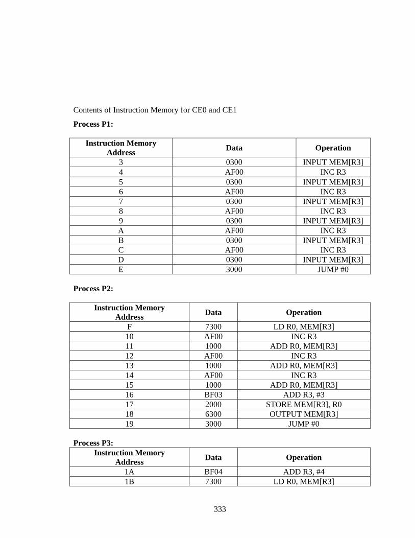
333
Contents of Instruction Memory for CE0 and CE1
Process P1:
Instruction Memory Address Data Operation
3 0300 INPUT MEM[R3] 4 AF00 INC R3 5 0300 INPUT MEM[R3] 6 AF00 INC R3 7 0300 INPUT MEM[R3] 8 AF00 INC R3 9 0300 INPUT MEM[R3] A AF00 INC R3 B 0300 INPUT MEM[R3] C AF00 INC R3 D 0300 INPUT MEM[R3] E 3000 JUMP #0
Process P2:
Instruction Memory Address Data Operation
F 7300 LD R0, MEM[R3] 10 AF00 INC R3 11 1000 ADD R0, MEM[R3] 12 AF00 INC R3 13 1000 ADD R0, MEM[R3] 14 AF00 INC R3 15 1000 ADD R0, MEM[R3] 16 BF03 ADD R3, #3 17 2000 STORE MEM[R3], R0 18 6300 OUTPUT MEM[R3] 19 3000 JUMP #0
Process P3:
Instruction Memory Address Data Operation
1A BF04 ADD R3, #4 1B 7300 LD R0, MEM[R3]
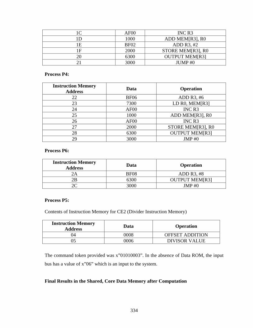
334
1C AF00 INC R3 1D 1000 ADD MEM[R3], R0 1E BF02 ADD R3, #2 1F 2000 STORE MEM[R3], R0 20 6300 OUTPUT MEM[R3] 21 3000 JUMP #0
Process P4:
Instruction Memory Address Data Operation
22 BF06 ADD R3, #6 23 7300 LD R0, MEM[R3] 24 AF00 INC R3 25 1000 ADD MEM[R3], R0 26 AF00 INC R3 27 2000 STORE MEM[R3], R0 28 6300 OUTPUT MEM[R3] 29 3000 JMP #0
Process P6:
Instruction Memory Address Data Operation
2A BF08 ADD R3, #8 2B 6300 OUTPUT MEM[R3] 2C 3000 JMP #0
Process P5: Contents of Instruction Memory for CE2 (Divider Instruction Memory)
Instruction Memory Address Data Operation
04 0008 OFFSET ADDITION 05 0006 DIVISOR VALUE
The command token provided was x”01010003”. In the absence of Data ROM, the input
bus has a value of x”06” which is an input to the system.
Final Results in the Shared, Core Data Memory after Computation

335
All Resulting Data and Data Address and in unsigned notation unless mentioned.
Process executed Resulting Data Data Address P2 24 10 P3 12 09 P4 36 11 P5 06 11
B.2 Application Two - Acyclic 2x 2 Matrix Multiplication Algorithms
Initialization tokens for the Look up Table – Sets of Table Load, Table Input and Load PRT tokens – For CE0:
Process Number Table Load Table Input Load PRT
P1 83f80003 83f04430 81d0030c P4 83f80213 83F10A60 81D00324 P7 83F8021A 83F1D090 81D0033C P10 83F80222 83F296C0 81D00354 P13 83F8022A 83F35C00 81D0036C P14 83F80032 83F38000 81D00374
For CE1:
Process Number Table Load Table Input Load PRT P1 82f80003 82f04430 81D0020B P4 82f80213 82F10A60 81D00223 P7 82F8021A 82F1D090 81D0023B P10 82F80222 82F296C0 81D00253 P13 82F8022A 82F35C00 81D0026B P14 82F80032 82F38000 81D00273
For CE3: Multiplier Processor
Process Number Table Load Table Input Load PRT P2 85F80104 85F08800 81D00514 P3 85F80106 85F0C800 81D0051C P5 85F80108 85F14E00 81D0052C P6 85F8010A 85F18E00 81D00534 P8 85F8010C 85F21400 81D00544 P9 85F8010E 85F25400 81D0054C P11 85F80110 85F2DA00 81D0055C P12 85F80112 85F31A00 81D00564

336
Contents of Instruction Memory for CE0 and CE1
Process P1:
Instruction Memory Address Data Operation
3 0300 INPUT MEM[R3] 4 AF00 INC R3 5 0300 INPUT MEM[R3] 6 AF00 INC R3 7 0300 INPUT MEM[R3] 8 AF00 INC R3 9 0300 INPUT MEM[R3] A AF00 INC R3 B 0300 INPUT MEM[R3] C AF00 INC R3 D 0300 INPUT MEM[R3] E AF00 INC R3 F 0300 INPUT MEM[R3] 10 AF00 INC R3 11 0300 INPUT MEM[R3] 12 3000 JUMP #0
Process P4:
Instruction Memory Address Data Operation
13 7300 LD R0, MEM[R3] 14 AF00 INC R3 15 1000 ADD R0, MEM[R3] 16 BF07 ADD R3, #7 17 2000 STORE MEM[R3], R0 18 6300 OUTPUT MEM[R3] 19 3000 JMP #0
Process P7:
Instruction Memory
Address Data Operation
1A BF04 ADD R3, #4 1B 7300 LD R0, MEM[R3] 1C AF00 INC R3 1D 1000 ADD MEM[R3], R0 1E BF04 ADD R3, #4 1F 2000 STORE MEM[R3], R0

337
20 6300 OUTPUT MEM[R3] 21 3000 JMP #0
Process P10:
Instruction Memory
Address Data Operation
22 BF02 ADD R3, #2 23 7300 LD R0, MEM[R3] 24 AF00 INC R3 25 1000 ADD MEM[R3], R0 26 BF07 ADD R3, #7 27 2000 STORE MEM[R3], R0 28 6300 OUTPUT MEM[R3] 29 3000 JMP #0
Process P13:
Instruction Memory Address Data Operation
2A BF06 ADD R3, #6 2B 7300 LD R0, MEM[R3] 2C AF00 INC R3 2D 1000 ADD MEM[R3], R0 2E BF04 ADD R3, #4 2F 2000 STORE MEM[R3], R0 30 6300 OUTPUT MEM[R3] 31 3000 JMP #0
Process P 14:
Instruction Memory
Address Data Operation
32 BF08 ADD R3, #8 33 6300 OUTPUT MEM[R3] 34 AF00 INC R3 35 6300 OUTPUT MEM[R3] 36 AF00 INC R3 37 6300 OUTPUT MEM[R3] 38 AF00 INC R3 39 6300 OUTPUT MEM[R3] 3A 3000 JMP #0

338
Contents of the Instruction Memory for the Multiplier CE- Process P 2: Multiplication
Instruction Memory Address Data Operation
04 0000 OFFSET ADDITION 05 000C MULTIPLICAND VAL
Process P 3: Multiplication
Instruction Memory Address Data Operation
06 0001 OFFSET ADDITION 07 0008 MULTIPLICAND VAL
Process P 5: Multiplication
Instruction Memory Address Data Operation
08 0004 OFFSET ADDITION 09 0005 MULTIPLICAND VAL
Process P 6: Multiplication
Instruction Memory Address Data Operation
0A 0005 OFFSET ADDITION 0B 001E MULTIPLICAND VAL
Process P 8: Multiplication
Instruction Memory Address Data Operation
0C 0002 OFFSET ADDITION 0D 000C MULTIPLICAND VAL
Process P 9: Multiplication
Instruction Memory Address Data Operation
0E 0003 OFFSET ADDITION 0F 0008 MULTIPLICAND VAL
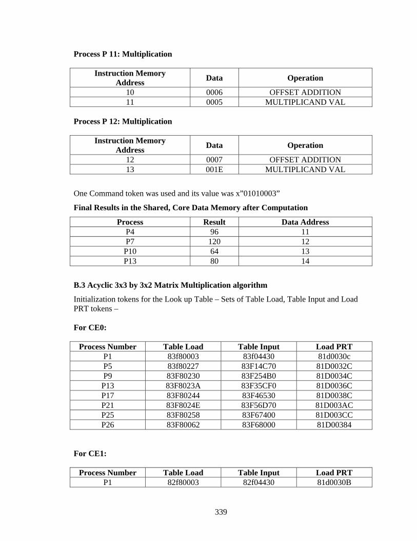
339
Process P 11: Multiplication
Instruction Memory Address Data Operation
10 0006 OFFSET ADDITION 11 0005 MULTIPLICAND VAL
Process P 12: Multiplication
Instruction Memory Address Data Operation
12 0007 OFFSET ADDITION 13 001E MULTIPLICAND VAL
One Command token was used and its value was x”01010003”
Final Results in the Shared, Core Data Memory after Computation
Process Result Data Address P4 96 11 P7 120 12 P10 64 13 P13 80 14
B.3 Acyclic 3x3 by 3x2 Matrix Multiplication algorithm
Initialization tokens for the Look up Table – Sets of Table Load, Table Input and Load PRT tokens – For CE0:
Process Number Table Load Table Input Load PRT
P1 83f80003 83f04430 81d0030c P5 83f80227 83F14C70 81D0032C P9 83F80230 83F254B0 81D0034C P13 83F8023A 83F35CF0 81D0036C P17 83F80244 83F46530 81D0038C P21 83F8024E 83F56D70 81D003AC P25 83F80258 83F67400 81D003CC P26 83F80062 83F68000 81D00384
For CE1:
Process Number Table Load Table Input Load PRT P1 82f80003 82f04430 81d0030B
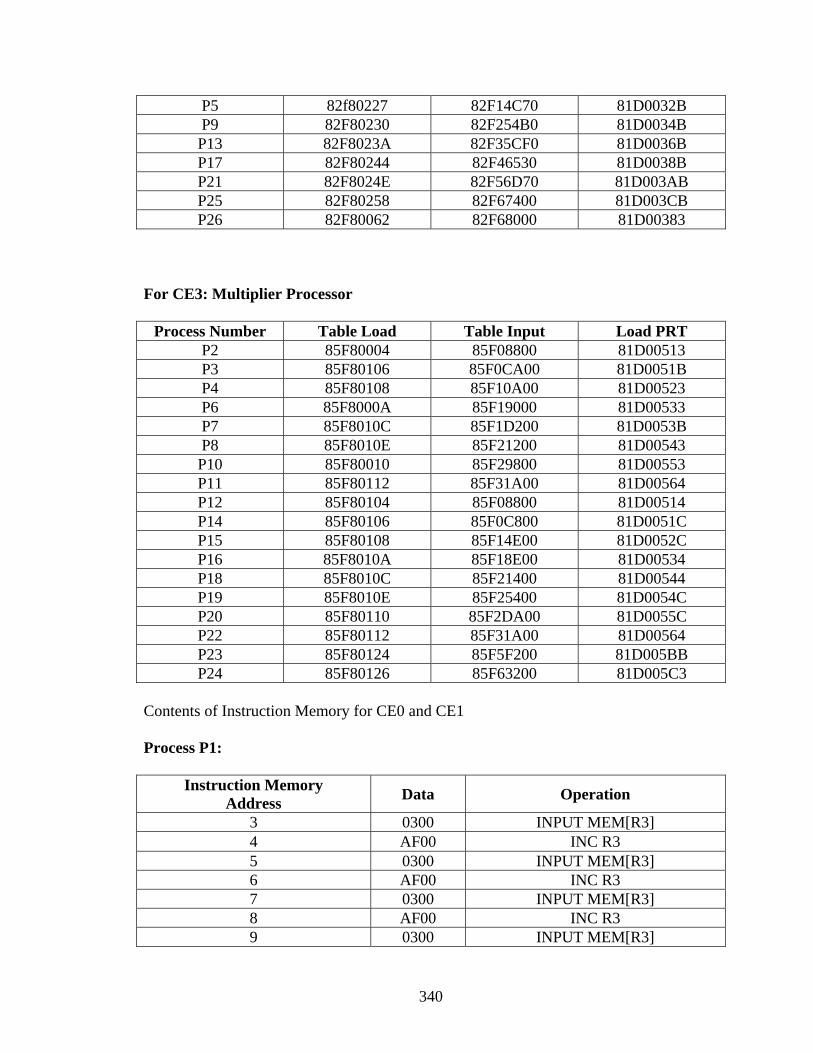
340
P5 82f80227 82F14C70 81D0032B P9 82F80230 82F254B0 81D0034B P13 82F8023A 82F35CF0 81D0036B P17 82F80244 82F46530 81D0038B P21 82F8024E 82F56D70 81D003AB P25 82F80258 82F67400 81D003CB P26 82F80062 82F68000 81D00383
For CE3: Multiplier Processor
Process Number Table Load Table Input Load PRT
P2 85F80004 85F08800 81D00513 P3 85F80106 85F0CA00 81D0051B P4 85F80108 85F10A00 81D00523 P6 85F8000A 85F19000 81D00533 P7 85F8010C 85F1D200 81D0053B P8 85F8010E 85F21200 81D00543 P10 85F80010 85F29800 81D00553 P11 85F80112 85F31A00 81D00564 P12 85F80104 85F08800 81D00514 P14 85F80106 85F0C800 81D0051C P15 85F80108 85F14E00 81D0052C P16 85F8010A 85F18E00 81D00534 P18 85F8010C 85F21400 81D00544 P19 85F8010E 85F25400 81D0054C P20 85F80110 85F2DA00 81D0055C P22 85F80112 85F31A00 81D00564 P23 85F80124 85F5F200 81D005BB P24 85F80126 85F63200 81D005C3
Contents of Instruction Memory for CE0 and CE1
Process P1:
Instruction Memory Address Data Operation
3 0300 INPUT MEM[R3] 4 AF00 INC R3 5 0300 INPUT MEM[R3] 6 AF00 INC R3 7 0300 INPUT MEM[R3] 8 AF00 INC R3 9 0300 INPUT MEM[R3]

341
A AF00 INC R3 B 0300 INPUT MEM[R3] C AF00 INC R3 D 0300 INPUT MEM[R3] E AF00 INC R3 F 0300 INPUT MEM[R3] 10 AF00 INC R3 11 0300 INPUT MEM[R3] 12 3000 JUMP #0
Process P4:
Instruction Memory Address Data Operation
13 7300 LD R0, MEM[R3] 14 AF00 INC R3 15 1000 ADD R0, MEM[R3] 16 BF07 ADD R3, #7 17 2000 STORE MEM[R3], R0 18 6300 OUTPUT MEM[R3] 19 3000 JMP #0
Process P7:
Instruction Memory
Address Data Operation
1A BF04 ADD R3, #4 1B 7300 LD R0, MEM[R3] 1C AF00 INC R3 1D 1000 ADD MEM[R3], R0 1E BF04 ADD R3, #4 1F 2000 STORE MEM[R3], R0 20 6300 OUTPUT MEM[R3] 21 3000 JMP #0
Process P10:
Instruction Memory
Address Data Operation
22 BF02 ADD R3, #2 23 7300 LD R0, MEM[R3] 24 AF00 INC R3 25 1000 ADD MEM[R3], R0 26 BF07 ADD R3, #7

342
27 2000 STORE MEM[R3], R0 28 6300 OUTPUT MEM[R3] 29 3000 JMP #0
Process P13:
Instruction Memory Address Data Operation
2A BF06 ADD R3, #6 2B 7300 LD R0, MEM[R3] 2C AF00 INC R3 2D 1000 ADD MEM[R3], R0 2E BF04 ADD R3, #4 2F 2000 STORE MEM[R3], R0 30 6300 OUTPUT MEM[R3] 31 3000 JMP #0
Process P 14:
Instruction Memory
Address Data Operation
32 BF08 ADD R3, #8 33 6300 OUTPUT MEM[R3] 34 AF00 INC R3 35 6300 OUTPUT MEM[R3] 36 AF00 INC R3 37 6300 OUTPUT MEM[R3] 38 AF00 INC R3 39 6300 OUTPUT MEM[R3] 3A 3000 JMP #0
Contents of the Instruction Memory for the Multiplier CE- Process P 2: Multiplication
Instruction Memory Address Data Operation
04 0000 OFFSET ADDITION 05 000C MULTIPLICAND VAL

343
Process P 3: Multiplication
Instruction Memory Address Data Operation
06 0001 OFFSET ADDITION 07 0008 MULTIPLICAND VAL
Process P 5: Multiplication
Instruction Memory Address Data Operation
08 0004 OFFSET ADDITION 09 0005 MULTIPLICAND VAL
Process P 6: Multiplication
Instruction Memory Address Data Operation
0A 0005 OFFSET ADDITION 0B 001E MULTIPLICAND VAL
Process P 8: Multiplication
Instruction Memory Address Data Operation
0C 0002 OFFSET ADDITION 0D 000C MULTIPLICAND VAL
Process P 9: Multiplication
Instruction Memory Address Data Operation
0E 0003 OFFSET ADDITION 0F 0008 MULTIPLICAND VAL
Process P 11: Multiplication
Instruction Memory Address Data Operation
10 0006 OFFSET ADDITION 11 0005 MULTIPLICAND VAL

344
Process P 12: Multiplication
Instruction Memory Address Data Operation
12 0007 OFFSET ADDITION 13 001E MULTIPLICAND VAL
One Command token was used and its value was x”01010003”
Final Results in the Shared, Core Data Memory after Computation
Result Data Address 30 96 34 97 93 98 94 99 156 100 154 101
B.4 Application Four - Acyclic Pipelined integer manipulation algorithm
For CE0:
Process Number Table Load Table Input Load PRT P1 83f80003 83f04430 81d0030c P2 83f80017 83F08800 81D00314 P3 83F80024 83F0CA00 81D0031B P6 83F80232 83F18E00 81D00334 P7 83F80039 83F1C000 81D0033C
For CE1:
Process Number Table Load Table Input Load PRT P1 82f80003 82f04430 81D0020B P2 82f80117 82F08800 81D00213 P3 82F80024 82F0CA00 81D0021C P6 82F80232 82F10E00 81D00233 P7 82F80039 82F1C000 81D0023D
For CE2:
Process Number Table Load Table Input Load PRT P5 84F80104 84F14C00 81D0042B
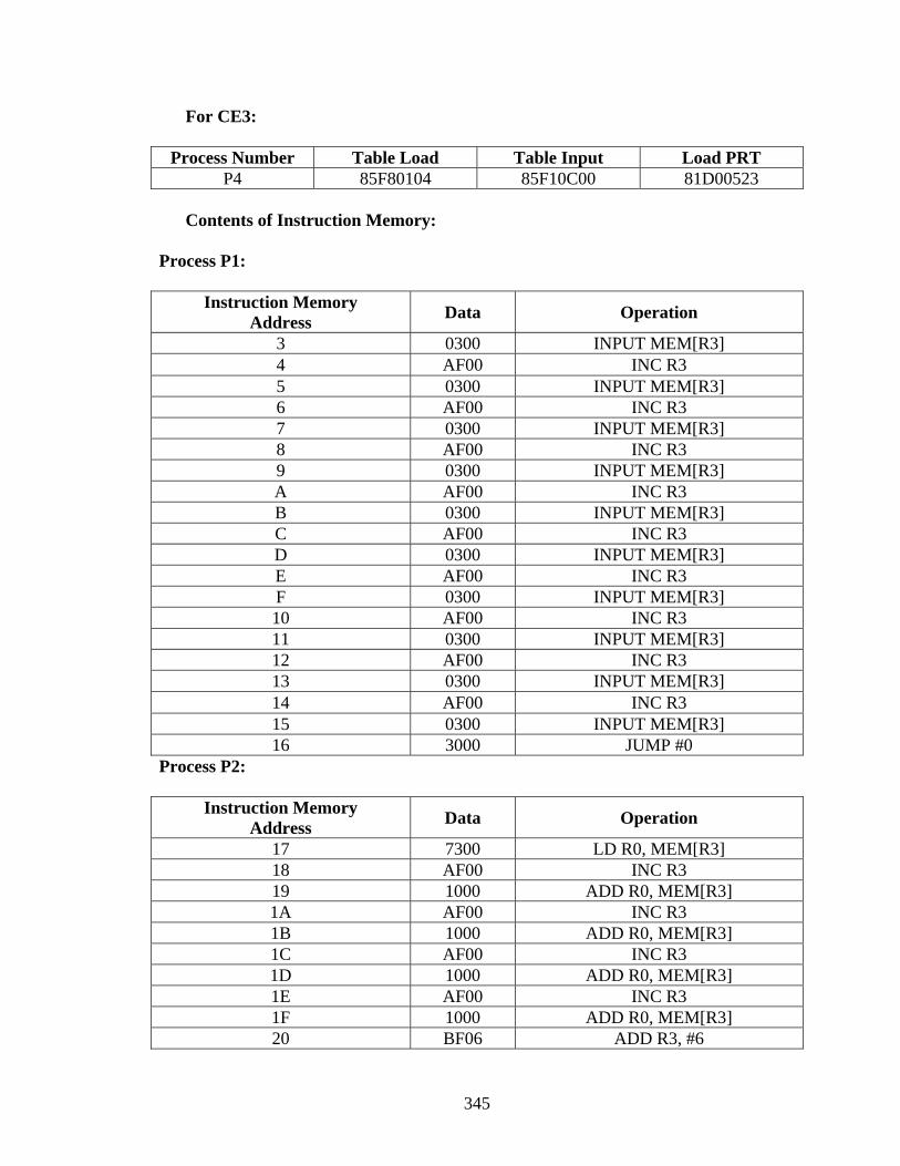
345
For CE3:
Process Number Table Load Table Input Load PRT P4 85F80104 85F10C00 81D00523
Contents of Instruction Memory:
Process P1:
Instruction Memory Address Data Operation
3 0300 INPUT MEM[R3] 4 AF00 INC R3 5 0300 INPUT MEM[R3] 6 AF00 INC R3 7 0300 INPUT MEM[R3] 8 AF00 INC R3 9 0300 INPUT MEM[R3] A AF00 INC R3 B 0300 INPUT MEM[R3] C AF00 INC R3 D 0300 INPUT MEM[R3] E AF00 INC R3 F 0300 INPUT MEM[R3] 10 AF00 INC R3 11 0300 INPUT MEM[R3] 12 AF00 INC R3 13 0300 INPUT MEM[R3] 14 AF00 INC R3 15 0300 INPUT MEM[R3] 16 3000 JUMP #0
Process P2:
Instruction Memory Address Data Operation
17 7300 LD R0, MEM[R3] 18 AF00 INC R3 19 1000 ADD R0, MEM[R3] 1A AF00 INC R3 1B 1000 ADD R0, MEM[R3] 1C AF00 INC R3 1D 1000 ADD R0, MEM[R3] 1E AF00 INC R3 1F 1000 ADD R0, MEM[R3] 20 BF06 ADD R3, #6

346
21 2000 STORE MEM[R3], R0 22 6300 OUTPUT MEM[R3] 23 3000 JMP #0
Process P3:
Instruction Memory Address Data Operation
24 BF05 ADD R3, #5 25 7300 LD R0, MEM[R3] 26 AF00 INC R3 27 1000 ADD MEM[R3], R0 28 AF00 INC R3 29 1000 ADD MEM[R3], R0 2A AF00 INC R3 2B 1000 ADD MEM[R3], R0 2C AF00 INC R3 2D 1000 ADD MEM[R3], R0 2E BF02 ADD R3, #5 2F 2000 STORE MEM[R3], R0 30 6300 OUTPUT MEM[R3] 31 3000 JMP #0
Process P6:
Instruction Memory Address Data Operation
32 BF0A ADD R3, #10 33 7300 LD R0, MEM[R3] 34 AF00 INC R3 35 5000 SUB MEM[R3], R0 36 AF00 INC R3 37 2000 STORE MEM[R3], R0 38 3000 JMP #0
Process P7:
Instruction Memory
Address Data Operation
39 BF0C ADD R3, #12 3A 6300 OUTPUT MEM[R3] 3B 3000 JMP #0
Process P4: Multiplication
Instruction Memory Address Data Operation

347
04 000A OFFSET ADDITION 05 0002 MULTIPLICAND VAL
Process P5: Division
Instruction Memory Address Data Operation
04 000B OFFSET ADDITION 05 0002 DIVISOR VAL
Here two command tokens are provided for pipelined execution and they are x”0101FF03” and x”0121FF11” Contents of the shared data memory initially and after computation for copy 1-
Address Location Initially before Multiplication and division
Result after multiplication and division
13 10 20 14 10 5
For the first copy of the application, shared data memory has a value of ‘2’ in ten locations from location ”03” to ”12”.The result after addition of first five numbers is stored in location “13” and similarly the result of the addition of the next five numbers is stored at “14”. The initial values before the multiplication and division processes are ten which get updated to “20” and “5” after the respective processes get over. Final result of 15 is store at location 15 for the first copy after subtraction of the above final results of multiplication and division Contents of the shared data memory initially and after computation for copy 2-
Address Location Result prior to Multiplication and Division
Results after Multiplication and Division
27 10 20 28 10 5
For the second copy of the application, shared data memory has a value of “2” in ten locations from “17” to “26”. Final result of “15” is store at location “29” for the first copy after subtraction of the above final results of multiplication and division B.5 Complex Non-Deterministic Cyclic Value Swap Application Initialization tokens for the Look up Table – Sets of Table Load, Table Input and Load PRT tokens –

348
For CE0:
Process Number Table Load Table Input Load PRT P1 83f80003 83f04440 81d0030c P2 83f8010D 83F08600 81D00314 P3 83F80014 83F0C406 81D0031C P4 83f8011B 83f10A00 81D00324 P5 83F80023 83F14806 81D0032C P6 83F8022A 83F18000 81D00334
For CE1:
Process Number Table Load Table Input Load PRT P1 82F80003 82F04440 81d0020B P2 82F8010D 82F08600 81D00213 P3 82F80014 82F0C406 81D0021B P4 82Ff8011B 82F10A00 81D00223 P5 82F80023 82F14806 81D0022B P6 82F8022A 82F18000 81D00233
Contents of Instruction Memory for CE0 and CE1
Process P1: Instruction Memory
Address Data Operation Comments
3 0300 INPUT MEM[R3] Data Location 3 has 60 4 AF00 INC R3 Go to location 4 5 0300 INPUT MEM[R3] Data Location 4 has 100 6 AF00 INC R3 Go to location 5 7 0300 INPUT MEM[R3] Data Location 5 has 10 8 AF00 INC R3 Go to location 6 9 0300 INPUT MEM[R3] Data Location 6 has 60 A AF00 INC R3 Go to location 7 B 0300 INPUT MEM[R3] Data Location 7 has 100 C 3000 JUMP #0 Go back to DL 3

349
Process P2:
Instruction Memory Address Data Operation
D 7300 LD R0, MEM[R3] E BF02 ADD R3, #2 F 1000 ADD MEM[R3], R0 10 Cf02 SUB R3, #2 11 2000 STORE MEM[R3], R0 12 6300 OUTPUT MEM[R3] 13 3000 JMP #0
Process P3:
Instruction Memory Address Data Operation
14 BF04 ADD R3, #4 15 7300 LD R0, MEM[R3] 16 CF04 SUB R3, #4 17 8000 IS R0= MEM[R3] 18 2000 STORE MEM[R3], R0 19 6300 OUTPUT MEM[R3] 1A 3000 JMP #0
Process P4:
Instruction Memory Address Data Operation
1b BF01 ADD R3, #1 1C 7300 LD R0, MEM[R3] 1D Af00 INC R3 1E 5000 SUB R0,MEM[R3] 1F CF01 SUB R3, #1 20 2000 STORE MEM[R3], R0 21 6300 OUTPUT MEM[R3] 22 3000 JMP #0
Process P5:
Instruction Memory Address Data Operation
23 BF03 ADD R3, #3 24 7300 LD R0, MEM[R3] 25 CF02 SUB R3,#2 26 8000 IS R0= MEM[R3] 27 2000 STORE MEM[R3], R0

350
28 6300 OUTPUT MEM[R3] 29 3000 JMP #0
Process P6:
Instruction Memory Address Data Operation
2A 7300 LD R0, MEM[R3] 2B 6300 OUPUT MEM[R3] 2C AF00 INCR R3 2D 6300 OUPUT MEM[R3] 2E 3000 JMP #0
One command token was entered for the test bench and its value was x”01010003”
Finally in the shared data memory, the data values are swapped corresponding to what they were initially entered. The initial and final values in the shared data memory and shown below Initial Shared Data Memory values
Data Memory Address Data Comments
03 60 Initial Temperature 1 04 100 Initial Temperature 2 05 10 Temperature Variance Rate
Final Shared Data Memory values
Data Memory Address Data Comments
03 100 Final Temperature 1 04 60 Final Temperature 2 05 10 Temperature Variance Rate

351
B.6 Application proving the concept of Multiple Forking for the HDCA Initialization tokens for the Look up Table – Sets of Table Load, Table Input and Load PRT tokens – For CE0
Process Number Table Load Table Input Load PRT P1 83f80003 83f04430 81d0030c P2 83f8000F 83F08E00 81D00314 P3 83F80016 83F0C850 81D0031C P4 83F80118 83F11000 81D00324 P5 83F80120 83F15000 81d0032C P8 83F80328 83F20C00 81D00344 P6 83F80230 83F18000 81D00334
For CE1
Process Number Table Load Table Input Load PRT P1 82f80003 82f04430 81d0020B P2 82f8000F 82F08E00 81D00213 P3 82F80016 82F0C850 81D0021C P4 82F80118 82F11000 81D00223 P5 82F80120 82F15000 81d0022B P8 82F80328 82F20C00 81D00243 P6 82F80230 82F18000 81D00234
For Multiplier CE
Process Number Table Load Table Input Load PRT P7 85f80104 85F1CC00 81d0053C
Process P1:
Instruction Memory Address Data Operation
3 0300 INPUT MEM[R3] 4 AF00 INC R3 5 0300 INPUT MEM[R3] 6 AF00 INC R3 7 0300 INPUT MEM[R3] 8 AF00 INC R3 9 0300 INPUT MEM[R3] A AF00 INC R3
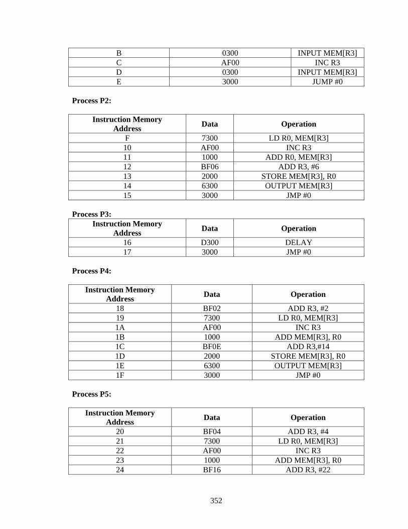
352
B 0300 INPUT MEM[R3] C AF00 INC R3 D 0300 INPUT MEM[R3] E 3000 JUMP #0
Process P2:
Instruction Memory Address Data Operation
F 7300 LD R0, MEM[R3] 10 AF00 INC R3 11 1000 ADD R0, MEM[R3] 12 BF06 ADD R3, #6 13 2000 STORE MEM[R3], R0 14 6300 OUTPUT MEM[R3] 15 3000 JMP #0
Process P3:
Instruction Memory Address Data Operation
16 D300 DELAY 17 3000 JMP #0
Process P4:
Instruction Memory Address Data Operation
18 BF02 ADD R3, #2 19 7300 LD R0, MEM[R3] 1A AF00 INC R3 1B 1000 ADD MEM[R3], R0 1C BF0E ADD R3,#14 1D 2000 STORE MEM[R3], R0 1E 6300 OUTPUT MEM[R3] 1F 3000 JMP #0
Process P5:
Instruction Memory Address Data Operation
20 BF04 ADD R3, #4 21 7300 LD R0, MEM[R3] 22 AF00 INC R3 23 1000 ADD MEM[R3], R0 24 BF16 ADD R3, #22
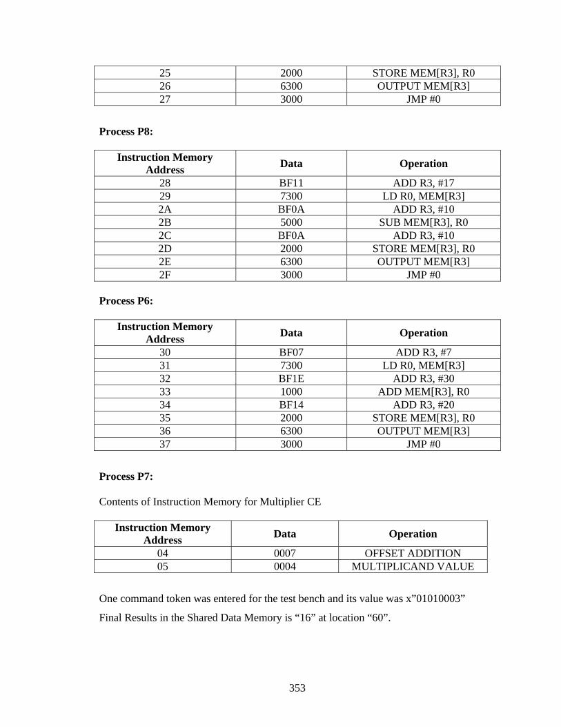
353
25 2000 STORE MEM[R3], R0 26 6300 OUTPUT MEM[R3] 27 3000 JMP #0
Process P8:
Instruction Memory Address Data Operation
28 BF11 ADD R3, #17 29 7300 LD R0, MEM[R3] 2A BF0A ADD R3, #10 2B 5000 SUB MEM[R3], R0 2C BF0A ADD R3, #10 2D 2000 STORE MEM[R3], R0 2E 6300 OUTPUT MEM[R3] 2F 3000 JMP #0
Process P6:
Instruction Memory Address Data Operation
30 BF07 ADD R3, #7 31 7300 LD R0, MEM[R3] 32 BF1E ADD R3, #30 33 1000 ADD MEM[R3], R0 34 BF14 ADD R3, #20 35 2000 STORE MEM[R3], R0 36 6300 OUTPUT MEM[R3] 37 3000 JMP #0
Process P7: Contents of Instruction Memory for Multiplier CE
Instruction Memory Address Data Operation
04 0007 OFFSET ADDITION 05 0004 MULTIPLICAND VALUE
One command token was entered for the test bench and its value was x”01010003”
Final Results in the Shared Data Memory is “16” at location “60”.

354
REFERENCES [1] J. R. Heath, J. Cline and J. Kennedy, "A Dynamically Alterable Topology Distributed
Data Processing Computer Architecture," Proceedings of the IEEE 1980 International Conference on Circuits and Computers, Port Chester, New York, pp.517-524, October 1-3, 1980.
[2] J. R. Heath and J. Cline, "The Complexity and Use of Multistage Interconnection
Networks for Distributed Processing Systems," Proceedings of the 1980 IEEE Distributed Data Acquisition, Computing, and Control Symposium, Miami Beach, Fl, pp.1-8, December 3-5, 1980.
[3] J. R. Heath, et. al., "A Dynamic Pipeline Computer Architecture for Data Driven
Systems: Final Report," Contract No. DASG60-79-C-0052, University of Kentucky Research Foundation, Lexington, Kentucky, February, 1982.
[4] A. D. Hurt and J. R. Heath, "A Data Flow Language and Interpreter for a
Reconfigurable Distributed Data Processor," Proceedings of 1982 IEEE International Conference on Circuits and Computers, New York, NY, pp.56-59, September 29 - October 1, 1982.
[5] A. D. Hurt and J. R. Heath, "The Design of a Fault-Tolerant Computing Element for
Distributed Data Processors," Proceedings of the 3rd IEEE International Conference on Distributed Computing Systems, Miami/Ft. Lauderdale, Florida, pp.171-176, October 18-22, 1982.
[6] J. R. Heath, A. D. Hurt, and G. D. Broomell, "A Distributed Computer Architecture
for Real-Time, Data Driven Applications," Proceedings of the 3rd IEEE International Conference on Distributed Computing Systems, Miami/Ft. Lauderdale, Florida, pp.630-638, October 18-22, 1982.
[7] A. D. Hurt and J. R. Heath, "A Hardware Task Scheduling Mechanism for a Real-
Time Multimicroprocessor Architecture," Proceedings 1982 IEEE Real-Time Systems Symposium, Los Angeles, California, pp.113-123, December 7-9, 1982.
[8] G. Broomell and J. R. Heath, "Classification Categories and Historical Development
of Circuit Switching Topologies," ACM Computing Surveys, Vol. 15, No. 2, June 1983, pp. 95-133.
[9] G. Broomell and J. R. Heath, "An Integrated-Circuit Crossbar Switching System
Design," Proceedings of 4th International Conference on Distributed Computing Systems, San Francisco, California, pp.278-287, May 14-18, 1984.
[10] James D. Cochran, “Mathematical Modeling and Analysis of a Dynamic Pipeline
Computer Architecture”, Masters Thesis, Department of Electrical Engineering, University of Kentucky, Lexington, KY, 1982.

355
[11] J. R. Heath, J. Cochran and W. A. Chren, Jr., "A Flow Graph Analysis Algorithm for
a Data Driven Reconfigurable Parallel Pipelined Computer Architecture," Proceedings IEEE Region III Southeastcon'89, Columbia, South Carolina, pp. 639-644, April 9-12, 1989.
[12] J. R. Heath and S. Ramamoorthy, "Design and Performance of a Modular Hardware
Process Mapper (Scheduler) for a Real-Time Token Controlled Data Driven Multiprocessor Architecture," Proceedings of the 23rd Southeastern Symposium on System Theory, Columbia, South Carolina, pp. 478-482, March 10-12, 1991.
[13] J.R. Heath, S. Ramamoorthy, C.E. Stroud, and A. Hurt, "Modeling, Design, and
Performance Analysis of a Parallel Hybrid Data/Command Driven Architecture System and its Scalable Dynamic Load Balancing Circuit", IEEE Trans. on Circuits and Systems, II: Analog and Digital Signal Processing, Vol. 44, No. 1, pp. 22-40, January, 1997.
[14] J.R. Heath and B. Sivanesa, "Development, Analysis, and Verification of a Parallel Hybrid Data-flow Computer Architectural Framework and Associated Load Balancing Strategies and Algorithms via Parallel Simulation", SIMULATION, Vol. 69, No. 1, pp. 7-25, July, 1997.
[15] Fernando, U. Chameera. "Modeling, Design, Prototype Synthesis and Experimental
Testing of a Dynamic Load Balancing Circuit for a Parallel Hybrid Data/Command Driven Architecture." Master's Project. University of Kentucky, December 1999.
[16] J.R. Heath and A. Tan, "Modeling, Design, Virtual and Physical Prototyping,
Testing, and Verification of a Multifunctional Processor Queue for a Single-Chip Multiprocessor Architecture", Proceedings of 2001 IEEE International Workshop on Rapid Systems Prototyping, Monterey, California, 6 pps. June 25-27, 2001.
[17] Xiaohui Zhao, J. Robert Heath, Paul Maxwell, Andrew Tan, and Chameera
Fernando, “Development and First-Phase Experimental Prototype Validation of a Single-Chip Hybrid and Reconfigurable Multiprocessor Signal Processor System”, Proceedings of the 2004 IEEE Southeastern Symposium on System Theory, Atlanta, GA, 5pps, March 14-16, 2004.
[18] André DeHon,”The Density Advantage of Configurable Computing”, IEEE
Computer, 33(4):41--49, April 2000 [19] Lara Simsic, “Accelerating algorithms in hardware”, Embedded.com, Jan 20, 2004. [20] Chiang, Anna S. "Programming Enters Designer's Core." Electrical Engineering
Times, 19 Feb. 2001, 5pps, 106 – 110. [21] Haynes, Simon D., et. al, "Video Image Processing with the Sonic Architecture."
IEEE Compute, Apr. 2000, 8pps, 50 - 57.

356
[22] Callahan, Timothy J., et. al,”The GARP Architecture and the C Compiler”, IEEE Computer, Apr 2000, 8pps, 62 – 69.
[23] Callahan, Timothy J. and John Wawrzynek. "Reconfiguring SoC According to
GARP", Electrical Engineering Times, 19 Feb. 2001, 82 - 120. [24] Gregory J Donohue, K. Joseph Hass et al, “A Reconfigurable Data Path Processor
for Space Applications”, Proceedings of Military and Aerospace Applications of Programmable Logic Devices 2000, Laurel, MD, September 24-28, 2000.
[25] Ligon, Walter B., et al., "Implementation and Analysis of Numerical Components
for Reconfigurable Computing", IEEE Aerospace Applications Conference Proceedings 2, 1999, 11pps, 325 - 335.
[26] Jürgen Becker, Manfred Glesner, Ahmad Alsolaim, Janusz Starzyk, Darmstadt
University of Technology and Ohio Universty,” Fast Communication Mechanisms in Coarse-grained Dynamically Reconfigurable Array Architectures”.
[27] J. R. Heath and E. A. Disch, "A Methodology for the Control and Custom VLSI
Implementation of Large Scale Clos Networks," Proceedings 1988 IEEE International Conference on Computer Design: VLSI In Computers and Processors, Rye Brook, New York, pp. 472-477, October 3-5, 1988
[28] J. R. Heath and S. Riley, "Modeling and Implementation of an N x N Clos-Type
Interconnect Network Employing a "Clashing" Control Procedure," Proceedings IEEE Region III Southeastcon'89, Columbia, South Carolina, pp. 1211-1215, April 9-12, 1989.
[29] Venugopal Duvvuri, “Design, Development, and Simulation/Experimental
Validation of a Crossbar Interconnect Network for a Single-Chip Shared Memory Multiprocessor Architecture”, Masters Project, University of Kentucky, Lexington, KY, June 2002.
[30] Xilinx Website, Internet Resources, http://www.xilinx.com. [31] Mentor Graphics Website, Internet Resources, http://www.mentor.com. [32] Bhide, Kanchan, “Design Enhancement and Integration of a Processor-Memory
Interconnect Network into a Single-Chip Multiprocessor Architecture” Masters Thesis, University of Kentucky, Lexington, KY, December 2004.
[33] Paul Maxwell, "Design Enhancement, Synthesis, and Field Programmable Gate
Array Post-Implementation Simulation Verification of a Hybrid Data/Command Driven Architecture", Masters Project, University of Kentucky, Lexington, KY, May, 2001

357
[34] Xilinx Data Sheets on Multipliers in Virtex 2 Chip family, Internet Resources, http://direct.xilinx.com/bvdocs/appnotes/xapp636.pdf.
[35] Xiaohui Zhao, “Hardware Description Language Simulation and Experimental
Hardware Prototype Validation of a First-Phase Prototype of a Hybrid Data/Command Driven Multiprocessor Architecture”, Masters Project, University of Kentucky, Lexington, KY, May2002.

358
Vita Author's Name - Sridhar Hegde Birthplace - Mangalore, India Birthdate - May 28, 1978 Education Bachelor of Science in Electrical and Electronics Engineering Manipal Institute of Technology July - 2000 Research Experience 02/2004 - 12/2004 Research Assistant Lexmark International Inc. Lexington, KY 12/2001 - 02/2004 Graduate Research Assistant University of Kentucky Lexington, KY Society Memberships Member, IEEE