Abstract of “Switching Activity Analysis and Optimization ...
134
Abstract of “Switching Activity Analysis and Optimization Methods for Promoting Functionally Appropriate Test and Delay Characterization in Digital Integrated Circuits” by Elif Alpaslan, Ph.D., Brown University, May 2011 This dissertation utilizes Design for testability, DFT-, and automatic test pattern generation, ATPG-based, techniques to overcome various problems that are caused by the non-functional switching activity of the circuit during scan-based test. Switching activity discrepancies between a circuit’s functional and test modes are problematic for a variety of reasons. When switching activity is excessive, it may damage chips or cause working parts to be considered defective—leading to yield loss. In other cases, very low switching activity during test may lead to test escapes. In this dissertation, the characteristics and the nature of the hazardous switching activity have been studied during circuit’s test and functional mode. A quantitative comparison of the amount and the profile of the switching activity for different modes of operation has been performed. Motivated by the outcomes of our activity analysis for scan shift, we developed a DFT-based technique which relies on inserting extra test points to a subset of the flip- flops in the verified circuit such that the transitions at the outputs of these selected flip- flops will be blocked from propagating to the combinational parts of the design. The proposed technique modifies the circuit at register-transfer level, RTL, such that the timing violations due to the inserted extra hardware will be handled by the synthesis tool. With the proposed method, the excessive switching activity during the shift cycles of the scan test will be reduced with an insignificant area overhead. We also developed a noise index model, NIM, which can be effectively used to capture the effects of the excessive switching activity around a critical path during the launch clock cycle on the delay of the path. We have validated the effectiveness of our noise index model on an industrial size circuit to estimate the delay discrepancies between the silicon measurements and pre-silicon simulation estimations. We then used our noise index model for high-quality path delay pattern generation by utilizing the large fraction of the don’t care bits in the test cubes. Through our noise index model based X’filling method, we replicated the worst observed
Transcript of Abstract of “Switching Activity Analysis and Optimization ...

Abstract of “Switching Activity Analysis and Optimization Methods for Promoting
Functionally Appropriate Test and Delay Characterization in Digital Integrated Circuits”
by Elif Alpaslan, Ph.D., Brown University, May 2011
This dissertation utilizes Design for testability, DFT-, and automatic test pattern
generation, ATPG-based, techniques to overcome various problems that are caused by
the non-functional switching activity of the circuit during scan-based test. Switching
activity discrepancies between a circuit’s functional and test modes are problematic for a
variety of reasons. When switching activity is excessive, it may damage chips or cause
working parts to be considered defective—leading to yield loss. In other cases, very low
switching activity during test may lead to test escapes. In this dissertation, the
characteristics and the nature of the hazardous switching activity have been studied
during circuit’s test and functional mode. A quantitative comparison of the amount and
the profile of the switching activity for different modes of operation has been performed.
Motivated by the outcomes of our activity analysis for scan shift, we developed a
DFT-based technique which relies on inserting extra test points to a subset of the flip-
flops in the verified circuit such that the transitions at the outputs of these selected flip-
flops will be blocked from propagating to the combinational parts of the design. The
proposed technique modifies the circuit at register-transfer level, RTL, such that the
timing violations due to the inserted extra hardware will be handled by the synthesis tool.
With the proposed method, the excessive switching activity during the shift cycles of the
scan test will be reduced with an insignificant area overhead.
We also developed a noise index model, NIM, which can be effectively used to
capture the effects of the excessive switching activity around a critical path during the
launch clock cycle on the delay of the path. We have validated the effectiveness of our
noise index model on an industrial size circuit to estimate the delay discrepancies
between the silicon measurements and pre-silicon simulation estimations.
We then used our noise index model for high-quality path delay pattern
generation by utilizing the large fraction of the don’t care bits in the test cubes. Through
our noise index model based X’filling method, we replicated the worst observed

functional switching activity profile around the critical path of interest. We used this
model to overcome the over-testing and under-testing problems of the path delay test.

Switching Activity Analysis and Optimization Methods for Promoting Functionally
Appropriate Test and Delay Characterization in Digital Integrated Circuits
by
ELIF ALPASLAN
B.S. Sabanci University, 2005
Sc. M. Brown University, 2007
A Dissertation submitted in partial fulfillment of the requirements for
the Degree of Doctor of Philosophy
in the Division of Engineering at Brown University
Providence, Rhode Island
May 2011

© Copyright
by
Elif Alpaslan
2011


iii
This dissertation by Elif Alpaslan is accepted in its present form by
the Division of Engineering as satisfying the
dissertation requirement for the degree of
Doctor of Philosophy
Date_____________ ______________________________________________ Jennifer Lynn Dworak, Director
Recommended to the Graduate Council
Date_____________ ___________________________________________ Iris Bahar, Reader
Date_____________ ___________________________________________ Desta Tadesse, Reader
Approved by the Graduate Council
Date_____________ ___________________________________________ Peter M. Weber, Dean of the Graduate School

iv
The Vita of Elif Alpaslan
Elif Alpaslan was born in Istanbul, Turkey on February 10, 1981. Upon completion of
high school, her undergraduate education took place at Sabanci University in Istanbul,
Turkey where only the top 0.5% of students taking the nationwide University Entrance
Exam were considered for admission to this university. She graduated from Sabanci
University in June 2005 with a B.S.E.E in Microelectronics Engineering. Shortly after
graduation, she received a Brown University Graduate Fellowship and arrived at Brown
University in September 2005. At Brown University, she joined the Laboratory for
Engineering Man/Machine Systems (LEMS) group as a research assistant, advised by
Professor Jennifer Dworak. She was awarded a Design Automation Conference (DAC)
Graduate Fellowship in July 2006. She completed the requirements for a Sc.M in
Engineering in 2007 at Brown University. She completed an engineering internship at
Mentor Graphics Corporation in Marlboro, MA in the summer of 2007. Her work during
this internship was published in VLSI Test Symposium (VTS) in 2008 and in IEEE
Transactions on Computer-Aided Design of Integrated Circuits and Systems in 2010. She
completed her second engineering internship at NXP Semiconductors in Eindhoven,
Netherlands between 2008 and 2009. Her work during this internship was published in
the proceedings of Design and Test in Europe (DATE).
.

v
Acknowledgements
I would like to express my most sincere appreciation to my advisor Jennifer Dworak at
Brown University. During this long journey she has been a great advisor to me in terms
of her scientific creativeness and her kind and understanding personality. Also special
thanks goes to my dissertation committee members, Professor Iris Bahar and Dr. Desta
Tadesse. I would also like to thank to the past and current members of our laboratory,
Kundan Nepal, Cesare Ferri, Yiwen Shi, Nuno Alves, Roto Lee and Octavian Biris for
their support and their friendship.
A very special thanks goes to my undergraduate advisor Ilker Hamzaoglu, for being
helpful in my decision process to continue with my education and become a PhD. His
VLSI classes and projects were the reason for my decision to continue my academic life
in the VLSI area.
I would like to thank my advisor Dr. Yu Huang at Mentor Graphics for giving me the
engineering internship opportunity at Mentor Graphics and for his feedback in our
project. I also want to acknowledge Dr. Ananta K. Majhi, Dr. Bram Kruseman and Paul
van de Wiel for being my advisors during my internship at NXP Semiconductors. The
quality of my project at NXP was significantly enhanced by their assistance.
Special thanks goes to James Eakin, and his parents Diane and James Eakin who have
been like a second family to me in the United States due to their support and love.
Finally, a very special thanks goes to my sister Ece Alpaslan and my parents Aynur and
Bayram Alpaslan for their never-ending love and support, and for always believing in
me. I would not have accomplished any of this without them.

1
Contents
Chapter 1 Introduction 7
1.1 Main Contributions ………………………………………………………….13
1.2 Organization of the Dissertation …………………………………...………..15
Chapter 2 Background 16
2.1 Scan-based Test ……………………………………………………………..19
2.2 Overhead of Scan-based Test ………………………………………………..21
2.3 Fault Models ………………………………………………………………...23
2.3.1 Stuck-at Faults …………………………………………………….23
2.3.2 Transition Delay Faults ……………………………………………26
2.3.3 Path Delay Faults ………………………………………………….28
2.4 Scan-based Delay Testing …………………………………………………...29
Chapter 3 Power Dissipation during Test 32
3.1 Test Power Reduction Techniques …………………………………………..33
3.1.1 ATGP-based Approaches ………………………………………….33
3.1.2 DFT-based Approaches …………………………………………...35
3.2 Comparison of the Switching Activity during Test and Functional Modes ...38
3.3 Power Sensitive Scan Cell Identification ……………………………………43
3.3.1 Signal Probability Approach ………………………………………43
3.3.2 TRR – Toggling Rate Reduction Metric …………………………..45

2
3.4 RTL Modification for Scan Shift Activity Reduction ………………………47
3.4.1 Identifying Power-Sensitive RTL Bits …………………………….49
3.4.2 Freezing Power-Sensitive RTL Bits ………………………………50
3.5 Experimental Results ………………………………………………………..55
3.5.1 Actual Shift Power Reduction …………………………………….56
3.5.2 Area Overhead of the Freeze Modification ……………………….61
3.5.3 Computational Complexity ………………………………………………..61
3.6 Summary …………………………………………………………………….63
Chapter 4 Unexpected Timing on Silicon 65
4.1 Delay Discrepancies between Silicon and Simulation ………………………67
4.2 Path Delay Measurements vs SPICE-Level Timing Analysis ………………69
4.3 The Noise Index Model ……………………………………………………..75
4.4 Flow for the Noise Index Model …………………………………………….81
4.5 Correlation between NIM and Delay Difference between Design Simulation
and Silicon ………………………………………………………………………82
4.6 Summary …………………………………………………………………….84
Chapter 5 High-quality At-speed Testing 85
5.1 High-quality Test Pattern Generation and Manipulation Techniques ………87
5.1.1 Pseudo-Functional Test ……………………………………………88
5.1.2 Power Supply Noise Aware Pattern Generation …………………..89
5.2 Noise Index Analysis for Functional and Test Modes ………………………90

3
5.3 NIM-X: NIM-based X-filling Algorithm …………………………………..100
5.4 Experimental Results ………………………………………………………105
5.5 Summary …………………………………………………………………...108
Chapter 6 Conclusion 110

4
List of Figures
Figure 2-1: The difference between the D-type flip flop and MUX-based scan flip
flop……………………………………………………………………………………20
Figure 2-2: Scan inserted design…………….………………………………….........21
Figure 2-3: Stuck-at fault example……… ………….……………………………….24
Figure 2-4: Stuck-at test timing scheme……………………………………………..18
Figure 2-5: Timing behavior for LOC delay test………………………………….….30
Figure 2-6: Timing behavior of LOS delay test………………………………………31
Figure 3-1: Simulation flow for functional inputs ………………….…………...…...39
Figure 3-2: Analysis flow for test patterns generated by ATPG……………………...41
Figure 3-3: Signal Probability Calculation……………………...……………………44
Figure 3-4: Procedure for calculating TRR………………………………………….. 46
Figure 3-5: Original Circuit…………………………………………...……………...48
Figure 3-6: Circuit after inserting an additional gate…………………………………48
Figure 3-7: Example of RTL modification in VHDL………………………………...52
Figure 3-8: Example of RTL modification in Verilog………………………………..53
Figure 3-9: Complete design flow with the proposed freeze modification method…..54
Figure 3-10: Total number transitions at the combinational gate outputs for the
unmodified and modified copies of the Ckt1…………………………...…………….57
Figure 3-11: Total number transitions at the combinational gate outputs for the
unmodified and modified copies of the Ckt2 ...…………………...……………….....58

5
Figure 3-12: Effect of the XOR/XNOR gates to the switching activity reduction ......59
Figure 4-1: Correlation between expected and measured path delays ……………….71
Figure 4-2: Switching activity profile of two different paths at launch cycle………..73
Figure 4-3: Switching activity profile of two slower than expected paths at launch
cycle…………………………………………………………………………………..74
Figure 4-4: Switching activity area of interest for the noise index model …………...77
Figure 4-5: Triangular shaped current profile ………………………………………..78
Figure 4-6: Voltage drop profile vs radius ……………………………………...……79
Figure 4-7: Flow for the noise index analysis ………………………………..………82
Figure 4-8: Delay difference vs. noise index values………………………………….83
Figure 5-1: Flow for VCD and DEF files generation …………………….……..…...91
Figure 5-2: Location of the robustly-detected critical paths …..…………..……...….97
Figure 5-3: Spatial activity profile for region 1 …………..…………..…..…...……98
Figure 5-4: Spatial activity profile for region 7 .…………………..……..…………99
Figure 5-5: Spatial activity profile for region 8 .……………………………………100
Figure 5-6: The NIM difference of the paths between functional and test modes…..102
Figure 5-7: Proposed NIM-based X-filling Method…………………...….………...103
Figure 5-8: NIM difference between path delay test vectors and functional patterns for
No-Fill and NIM-Fill for color converter benchmark……………………………….105
Figure 5-9: NIM difference between path delay test vectors and functional patterns for
No-Fill and NIM-Fill for FPU benchmark…………………………………………..106

6
List of Tables
Table 3-1 Average Number of Transitions per Clock Cycle during Functional
Operation…………………………………………………………………………….. 40
Table 3-2 Average Number of Transitions per Clock Cycle for ATPG Patterns…….42
Table 3-3 Characteristics of the Circuits…….………………………………………..55
Table 3-4 Actual Reduction in Switching Activity at Combinational Part of the Circuit after Freezing Power-Sensitive Scan Cells………………………………...…………60
Table 3-5 Area Overhead of the Freeze Modification………………………………. 61
Table 5-1 Average and Maximum Number of Transitions during Functional
Operation……………………………………………………………………………...93
Table 5-2 Average Number of Transition during the Path Delay Test Mode….……..94
Table 5-3 The Average of the Absolute Values of NIM Differences for Different Fill
Options………………………………………………………………………………107

7
Chapter 1
Introduction
In 1965, Gordon Moore predicted that the total number of transistors that can be placed
on a single chip would double every two years [1]. Since then, the semiconductor
industry has poured significant resources into making that prediction come true. The
switching speed of the transistors has increased, and smaller device sizes have enabled
the designers to fit more transistors into the same area. This has lead to exponential
increases in performance. At the same time, because today’s chips experience more
simultaneous switching per unit area, there has been a dramatic increase in the power
densities of today’s high performance designs.
As a result, reducing power dissipation and power supply switching noise has become
an important design consideration in current system-on-a-chip (SoC) designs [5]. High
power dissipation leads to shorter battery lifetimes and requires expensive
cooling/packaging methods. Switching activity can also alter the delay characteristics of
the chip, making predictable design for a desired clock frequency difficult. As a result,
VLSI circuit designers have exploited multiple low power design methods at different

8
levels of the design process. At the same time, reducing power dissipation during test has
become especially critical as inappropriate switching activity during test can jeopardize
the accuracy of the tests, and in some cases, even destroy the chip.
According to the International Technology Roadmap for Semiconductors, testing of
today’s high performance chips is one of the most expensive, time-consuming and
challenging aspects of the overall design cycle [3]. The essential goal of manufacturing
test is to detect defective or “out-of-spec” chips by generating and applying high quality
test patterns at a minimum cost with respect to test application time and test data volume
[6]. The costs of manufacturing test correspond primarily to the time and effort required
to generate the high quality test patterns, the cost of the test equipment, and the
throughput or time required to apply the tests on the test floor. Testability features are
added to digital designs to make the development and application of manufacturing tests
easier and more effective. Unfortunately, they also make matching power during test and
functional operation more difficult.
Design for testability (DFT) techniques help the test engineers to achieve a high
quality test with a minimum usage of testing resources. One of the simplest DFT
approaches consists of Ad-Hoc DFT methods, where good design practices that are
learned from previous design experiences are used in the current circuit design cycle [6].
Unfortunately, the growing size and complexity of digital circuits makes the usage of the
Ad-Hoc DFT methods inadequate for high quality test. As a result, structured DFT
methodologies are a critical component of modern design flows.

9
Structured DFT methods rely on the insertion of the extra logic and signals into the
circuit to improve the testability of the design. Scan-based design is one of the most
widely-used structured DFT techniques for the manufacturing test of digital circuits. It
introduces a new mode to circuit operation—a test mode that is distinct from functional
mode. It reduces the complexity of the test by enhancing the controllability and
observability of the internal nodes of the design. Flip-flops in the design are connected
together into a large shift register, called a scan chain, which allows the circuit to be
initialized to an arbitrary state during test mode and allows the values of all of the flip-
flops, in addition to the outputs of the circuit, to be observed after the application of each
test pattern.
One of the major drawbacks of scan-based test is the increase in the circuit’s switching
activity during the shifting of the scan chain. There are multiple reasons for this
phenomenon. First, the test vectors applied consecutively are not correlated [7]. Second,
non-functional states may be traversed during the testing of the circuit. Furthermore, test
compaction and testing multiple cores simultaneously also contribute to higher switching
activity during test [8].
Unfortunately, increased test power due to excessive switching activity during scan
shift can create hot spots that may damage the silicon, the bonding wires and even the
package. It can also cause intensive erosion of conductors – severely decreasing the
reliability of the device. Furthermore, thermal spots have an adverse affect on the
carrier’s mobility which will eventually slow down the device in the hot-spot region of
the design. Elevated power dissipation and temperature variations in the circuit might
cause timing variations during the test mode that are different from the functional mode –

10
leading to yield loss due to inaccurate testing. As a result, some chips that would perform
well during normal operation may be rejected during test. Finally, the scan clock signal
may experience additional delays caused by supply voltage droop. This could cause scan
chain hold time violations during scan shifting when the delay of the clock signal is
larger than the scan cell hold time margin.
As a result, researchers have proposed various techniques to minimize the power
dissipation of the circuit during scan shift. These power reduction techniques can be
classified into two main categories, DFT-based approaches and ATPG-based approaches.
ATPG-based power reduction solutions [15-48] attempt to reduce the test power
dissipation by changing the characteristics of the test patterns applied to reduce the
switching activity. DFT-based power reduction techniques require either the
segmentation of the conventional scan chain architecture [49-56] or the insertion of
additional hardware into the original design [57-62] .
While it is known that switching activity during scan shift can easily exceed the
switching activity during functional mode, a detailed analysis of this difference has been
missing in the literature. This dissertation quantitatively analyzes the nature of the
switching activity of a circuit for functional and test modes to characterize the magnitude
of the discrepancy. Motivated by this switching activity analysis, we develop a novel and
effective DFT-based power reduction method for reducing the switching activity of the
scan-based test during the shift cycles at very low cost. Previous DFT-based power
reduction techniques rely on inserting extra test points into the verified design at the gate
level; however the insertion of extra hardware at the gate level will add extra delay that

11
may violate the timing requirements of the design. This new methodology makes changes
at the RTL instead of the gate level, providing standard synthesis tools with the ability to
automatically compensate for the added logic.
Reducing the timing discrepancy between design simulation and silicon measurements
is another fundamental challenge of current VLSI technology. With the decreasing noise
and timing margins of current VLSI chips, the performance of the chips has become more
susceptible to excessive switching activity. Making accurate predictions of silicon timing
through the use of pre-silicon modeling and analysis has become a very difficult
undertaking. The ultimate goal of the timing predictions during the design phase is to
estimate the delay of the critical paths on silicon. Unfortunately, current static timing
analysis (STA) tools generally have difficulty predicting the actual delays of the circuit
paths as well as finding the real speed-limiting critical paths of final silicon [9, 10].
Mismatches between silicon measurements and simulation are problematic for variety of
reasons. It makes it harder to predictably design the circuits so that they meet timing
specifications at first-silicon. In addition, it makes silicon debug a more arduous process.
When predicted and post-silicon delays do not match, the problem can be handled by
adding safety margins to designs, typically at the cost of area and performance, by selling
lower performing chips for less cost, or by re-spinning the design. Unfortunately, each of
these solutions is very expensive. As a result, multiple researchers have studied delay
mismatches and attempted to design complex tools to take into account various factors
causing the delay mismatches so that pre-silicon delay predictions can be improved [69 -
86]. However, these complex solutions suffer from practicality and scalability issues. In
this dissertation we develop a noise index model (NIM) which efficiently focuses on the

12
effects of the switching activity-generated IR-drop in the appropriate area around a path
on the actual delay of the circuit paths and estimates the magnitude of the timing
discrepancies due to switching activity.
The impact of switching activity on delay is not only a problem in the design phase. It
is also a problem in the test phase. When scan-based tests are applied, the switching
activity in the circuit during test application may not match the switching activity during
the circuit’s functional mode of operation. This can lead to changes in the delays of
tested paths and cause overtesting. For example, the performance of the chip during test
may be adversely affected by the IR-drop due to the high switching activity. The design
may fail to meet aggressive timing requirements when the supply voltages of the
transistors are reduced by the excessive IR-drop.
Over-testing may cause the circuit to be declared defective even when the chip would
work correctly during its functional mode. This problem can be solved at design time, but
at significant cost. For example, the designers may over-design the chip and power
distribution network by making the power rails of the power distribution network larger
or by increasing wiring pitch [11]. The timing slack may also be increased at the cost of
performance. Over-testing might also cause a loss of revenue even when chips are not
discarded as faulty, such as when the high frequency chips are incorrectly characterized
as lower speed chips and must be sold at lower prices [10].
In order to handle the yield and revenue loss problem, low power ATPG techniques
can be used to minimize the overall switching activity of the circuit during test [15-48].
However power-aware test vectors may also lead to under-testing problems. Some of the

13
chips containing speed-related problems may pass manufacturing test when the power
supply noise effects around the critical paths of the chip are reduced below functional
usage. As a result, in addition to yield loss, test escapes may also occur during delay
testing as a result of non-functional switching activity.
A significant amount of research effort has been directed to the generation of power
supply noise aware test vectors [43-48] and to the generation of pseudo-functional test
vectors [94-100]. These methods have often tried to simply minimize the switching
activity in the entire circuit during test. In other cases, they have relied on either vector-
less analysis of the circuit to estimate its functional mode switching activity, or they have
used designer-specific threshold values, which are based on the average switching
activity of the standard cells, for limiting switching activity. In this dissertation, we
investigate and quantitatively compare the noise index values of the critical paths during
functional and test modes. Based on this analysis we then propose a noise index model-
based test pattern modification technique that aims to generate high-quality test vectors
by reducing the over-testing and under-testing problems simultaneously.
1.1 Main Contributions
In this dissertation, we quantitatively compare the amount of switching activity during
test and functional mode both in the circuit as a whole and in the relevant area around
particular paths. We characterize the effect of local path switching activity on the
realized silicon delay. We then develop DFT-based and ATPG-based algorithms for
reducing the effects of switching activity-generated IR-drop and power consumption

14
during scan-based test to both protect the chip during scan shift and to reduce the impact
of over- and under-testing of the chip during the application of delay test patterns.
More specifically, the main contributions of this dissertation can be summarized as
follows:
• We focus our research efforts on the development of high level techniques to
reduce the effects of excessive switching activity during scan shift.
Specifically, we develop a DFT-based technique to reduce the switching
activity of the circuit during the shift cycles of the scan-based design. The
proposed DFT technique modifies the design at the RT-level such that the
synthesis tools can later be utilized for the automatic optimization of the timing
closure.
• We develop a noise index model (NIM) that characterizes the magnitude of the
timing mismatch between silicon and simulation based upon the switching
activity in a well-defined area around a critical path. We have validated the
effectiveness of this model on an industrial size circuit.
• We perform a detailed quantitative comparison of the switching activity with
respect to the noise index model on multiple benchmark circuits during
functional and test modes. Our comprehensive switching activity investigation
considers the effects of non-functional transitions in addition to the functional
transitions.
• Using the proposed noise index model, we develop an ATPG-based method to
help overcome the over-testing and under-testing problems of digital circuits.

15
Our noise index model-based pattern modification algorithm relies on the true
functional switching of the circuit such that the worst case functional switching
activity profile around the critical path of interest will be replicated during path
delay test. Our noise index model based test pattern modification method will
improve the quality of the at-speed delay test patterns.
1.2 Organization of the Dissertation
Chapter 2 provides background information about some of the important scan-based test
concepts and major fault models that have been used in manufacture testing. After the
introduction on scan-based test and important fault models, Chapter 3 explores previous
work on DFT- and ATPG-based test power reduction techniques during scan test and
then introduces a quantitative analysis on the nature of the switching activity of a circuit
operated in functional and test modes. In this chapter, we also introduce our RT-level
DFT-based approach to reduce the switching activity of the circuit during the shift cycles
of the scan test. Chapter 4 examines previous work on reducing timing mismatches
between silicon measurements and design simulations and then presents our noise index
model which characterizes the magnitude of the timing mismatch between silicon and
simulation. Chapter 5 presents our high-quality test pattern modification method, which
is based on our noise index model. Past research on switching activity aware test pattern
generation and modification techniques have been presented in this chapter. Finally,
chapter 6 offers some conclusions and future research ideas that have emerged through
these projects.

16
Chapter 2
Background
Power Analysis
Power dissipation in CMOS circuits has two components: static power dissipation and
dynamic power dissipation. Static power dissipation is primarily due to sub-threshold
conduction of current and occurs even when the circuit is not changing its state. In
contrast, dynamic power dissipation is generated when the circuit changes its logical
state, causing circuit switching. Although reducing static power dissipation has become
increasingly important—especially in ultra low-power designs, dynamic power
dissipation is still generally the dominant source of the overall power dissipation. It is
also a principal concern in power-aware testing since it is the dynamic power dissipation
that differs significantly between test and functional mode.
Dynamic power depends on the power supply voltage Vdd, the system clock frequency
f, the physical capacitance per unit area C, and the switching activity factor a. The
equation for the dynamic power dissipation is given as:

17
f)CV(P dddynamic α2
21
= (1.1)
Lowering any of these parameters will result in a reduction of the dynamic power
dissipation in the circuit. However, doing so effectively may be difficult both due to the
demands of today’s designs and the complex interdependencies that exist between the
parameters. In general, the parameter that is of most interest during power-aware test is
the switching activity factor a, as it is this parameter that changes significantly between
the test and functional modes of operation. It is also the only parameter that the test
engineer has any control over.
As power supply voltages decrease, the noise margin of the devices reduces
accordingly, making the design more vulnerable to power supply noise (PSN).
Understanding the impacts of the power supply noise on VLSI circuits involves
investigating the power supply network’s response to a sudden change in the current flow
in the circuit. Power supply noise has two components, inductive noise, also known as
Ldi/dt noise, and resistive noise, which is also known as IR-drop. Both the inductive and
resistive noises are due to the package and on-chip parasitics of the power/ground
network. The inductive noise, Ldi/dt, is due to the rate of change of the instantaneous
current flowing through power/ground networks in short time, and is dominant at the
package level of the chip. The resistive noise, IR-drop, refers to the amount of decrease in
the power rail voltage.
An increase in switching activity inside the chip leads to higher current densities in the
power distribution network. Power distribution networks also suffer from voltage
fluctuations due to the rapid changes in the supply current caused by large switching

18
activities inside the design. Specifically, because of the resistive effects of the power
supply network, voltage is reduced locally inside the chip due to current traveling from
the power pads to the core area in the design. Similarly the resistive ground network will
experience a voltage increase as current travels through it. The performance and
reliability of the circuit are adversely affected from both of the voltage drop in the power
supply network and voltage spike in the ground network. The IR drop will reduce the
voltage difference between the VDD and VSS pins of the standard cells, leading to a
reduction in standard cell’s performance. For example, the authors of [4] showed how the
delays of the circuits are affected by the supply voltage changes; specifically, for 90nm
technology, a 1% change in power supply voltage leads to a 4% change in the delay of a
circuit. Thus, in addition to potentially damaging the chip, changes in non-functional
switching activity may change the delay characteristics of a device during test.
Testing
The main goal of the manufacturing test is to ensure that a digital circuit fabricated on
silicon behaves according to the designer’s specifications. A high-quality manufacturing
test procedure should identify all the defective chips. As the complexity of current VLSI
systems increase, generating high-quality test vectors with good coverage becomes more
complicated and resource-intensive as well. The test generation problem becomes even
more complex in the case of sequential circuits because it is very difficult to control and
observe the internal states of the memory elements in sequential circuits. Therefore,
different types of design-for-testability techniques have been proposed for alleviating
some of the complex problems of manufacturing test.

19
Scan-based test is one of the most widely accepted design-for-testability techniques.
Additional logic is added to the design such that the controllability and observability of
the design will increase during the test of the circuit. Unfortunately scan-based tests often
cause excessive switching activity compared to the circuit’s normal operation. This
increase in switching activity results in additional challenges in manufacture testing of
digital circuits.
In the remainder of this chapter we will describe the essential concepts of scan-based
test and the most commonly used fault types for manufacturing test. The fundamentals
that are described in this chapter will be used in the subsequent chapters of the
dissertation when we will explain our methodologies.
2.1 Scan-based Test
The application of the scan-based test into the manufacturing test area was introduced by
Michael Williams and James Angell in 1973 [12]. The goal of the scan test is to simplify
the complex sequential automatic test pattern generation problem by introducing some
internal modifications to the original design. For a sequential design to have scan
capability, certain internal modifications have to be introduced into the original design.
This internal modification of the design starts with replacing the original sequential
elements, D-type flip flops, with scan flip-flops/cells which are later stitched together to
form a shift register, called a scan chain. One of the most widely used approaches to
convert D-type flip flops into scan flip flops is by using MUX-based scan cells. Figure
2-1 illustrates the difference between a standard D-type flip flop and a MUX-based scan

20
flip flop. An additional multiplexer is added to the original flip flop in order to select
between the test or normal mode of operation. Two additional primary inputs, called
scan_enable and scan_in, and one additional primary output, scan_out, are added to the
original design.
D Q D QD
SI
SE
CLK CLK
D-type FF MUX-based Scan-type FF
D Q D QD
SI
SE
CLK CLK
D-type FF MUX-based Scan-type FF
Figure 2-1: The difference between the D-type flip flop and MUX-based scan flip flop
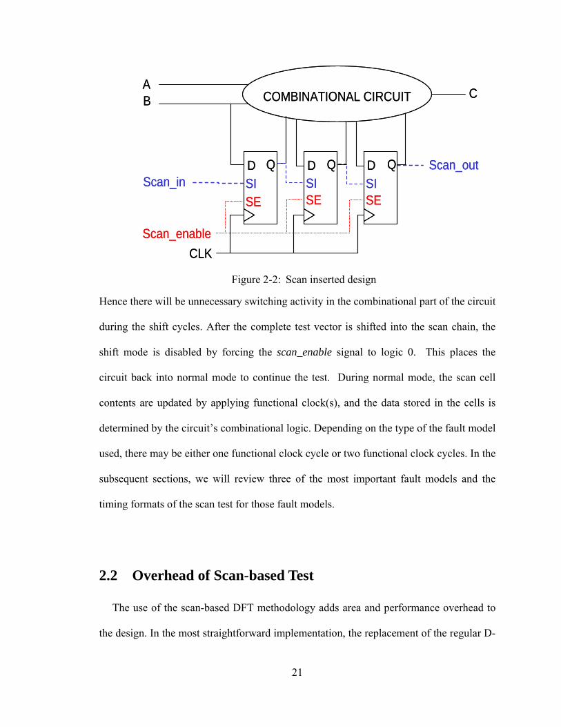
Figure 2-2 illustrates a small example for the scan inserted circuit. The scan_enable
signal is connected to the SE pin of the scan flip flop in order to control test and normal
mode. And the scan_in signal is connected to the SI pin of the scan cell. As we have
pointed out before, in addition to the circuit’s functional operation, scan-inserted designs
also operate in an additional mode called test mode. When the circuit operates in test
mode, the states of the scan flip-flops can be set to any logic value by shifting the logic
states through the scan_in input of the shift register. To allow the shift operation, first the
scan flip-flops are put into the shift mode through scan_enable signal. Test stimuli/test
responses are loaded into/unloaded from the scan chain during these shift cycles of the
test mode. During scan shift, the test stimuli are shifted into the scan chains one bit at a
time, and they create transitions at the scan cell outputs that are further rippled through
the combinational part of the circuit.
21
CLK
AB CCOMBINATIONAL CIRCUIT
D Q D Q D Q
SE SE SESI SI SI
Scan_enable
Scan_inScan_out
CLK
AB CCOMBINATIONAL CIRCUIT
D Q D Q D Q
SE SE SESI SI SI
Scan_enable
Scan_inScan_out
Figure 2-2: Scan inserted design
Hence there will be unnecessary switching activity in the combinational part of the circuit
during the shift cycles. After the complete test vector is shifted into the scan chain, the
shift mode is disabled by forcing the scan_enable signal to logic 0. This places the
circuit back into normal mode to continue the test. During normal mode, the scan cell
contents are updated by applying functional clock(s), and the data stored in the cells is
determined by the circuit’s combinational logic. Depending on the type of the fault model
used, there may be either one functional clock cycle or two functional clock cycles. In the
subsequent sections, we will review three of the most important fault models and the
timing formats of the scan test for those fault models.
2.2 Overhead of Scan-based Test
The use of the scan-based DFT methodology adds area and performance overhead to
the design. In the most straightforward implementation, the replacement of the regular D-

22
type flip-fops with multiplexer-based scan cells adds four additional gates to each flip-
flop. In addition to the increase in gate count, additional routing effort needs to be made
for the scan_enable signal. Scan-based design also impacts the performance of the
circuit. The usage of the multiplexers for every flip flop adds additional delay to the
circuit.
In the full scan methodology, all the sequential elements will be replaced with scan
cells and then stitched together in order to form the scan chain. The full scan
methodology is a fully automated process and thus requires very little manual effort.
However, the area and timing constraints of the design may not allow the usage of the
full scan approach. Alternatively, only a fraction of the sequential elements of the design
can be replaced with scan cells and then stitched into a scan chain. This approach is
called partial scan. Using the partial scan method, the testability of the sequential design
is increased with less impact on the area and timing of the design. For the critical parts of
the design where additional delay can not be tolerated, the flip flops that are physically
located in these critical areas can be excluded from the scan chain. Compared to the full
scan method, partial scan testing requires more ATPG effort for test vector generation.
Based on the area and performance budget of the design, the test engineer must select an
optimal approach for the scan methodology. In this work, we will only consider full-scan
designs.

23
2.3 Fault Models
2.3.1 Stuck-at Faults
Stuck-at faults are one of the most widely used fault models in the area of digital circuit
test because of the effectiveness of test patterns targeted toward them at finding most
common static defects in chips. Static defects are characterized by the fact that they
transform a circuit which realizes the intended function into a circuit that no longer
realizes that function. In other words, for some input combination, the defective circuit
will produce incorrect values at the outputs. When using the stuck-at fault model, the
digital circuit is modeled as interconnections between logical gates. The stuck-at fault
model is associated with these interconnections. In the case of fanout, a branch is
considered a distinct location from the stem. There are two types of stuck-at faults:
stuck-at 0 and stuck-at 1. For the stuck-at 0 fault, the signal line will always remain at a
logical state 0 irrespective of the correct logic output of the driving gate. For the stuck-at
1 fault, the reverse situation exists. Figure 2-3 shows an example circuit having a stuck-at
1 fault at its primary input line A.

24
AS
B
f
P
Q
A s-a-1
0 0/1
1 1/1
0/0
0/10/0
0/1
X
AS
B
f
P
Q
A s-a-1
0 0/1
1 1/1
0/0
0/10/0
0/1
X
Figure 2-3: Stuck-at fault example
The detection of stuck-at faults, like any other faults, has to meet two conditions:
excitation and observation. The excitation, also known as activation, of the stuck-at faults
involves forcing the faulty line to an opposite value from the actual fault value in the non-
faulty circuit. For example in Figure 2-3, the input signal A with the stuck-1 fault has to
be set to a logic 0 value, in order to excite this fault. After the excitation of the fault at a
particular site, the effect of the fault has to be propagated through a path to a primary
output (PO) or pseudo-primary output (PPO)—generally a scan flip-flop. This is called
observation. In order to observe the fault in Figure 2-3, input S is set to the required logic
value, so that the effect of fault is propagated to the primary output. When both of these
requirements are met, the fault can be detected. The detection of the stuck-at faults for
scan-based test requires application of one clock cycle in the normal mode between the
shift operations. The clocking scheme for stuck-at faults during scan-based test is shown
in Figure 2-4. The applied clock frequency for stuck-at faults is much slower than the
functional clock frequency because stuck-at faults do not affect the timing behavior of the
circuit. The test sets that are developed for detecting stuck-at faults may uncover many

25
static manufacturing defects and will ensure the logical correctness of the design.
However stuck-at fault test sets can not detect dynamic manufacturing defects which will
affect the timing behavior of the design. The presence of the defect does not alter the
function realized by the circuit over the long term, but it causes the circuit to slow down.
With the dominance of the timing related defects in current nanometer integrated
circuits (ICs), delay testing has become very popular in recent years. The delay of the
combinational logic in the circuit might exceed the clock period when the circuit has a
delay defect or when process variations impact the timing behavior of the circuit. For
correct circuit operation, the delay of the combinational logic in the circuit should not
exceed the clock period. In order to guarantee the timing correctness of the design, at-
speed testing in which the test patterns are applied to the design under test (DUT) at a
functional clock speed is essential. Transition delay fault (TDF) and path delay fault
(PDF) models are the most commonly used models in at-speed delay testing. In the next
sections, we will review these delay fault models in more detail.

26
CLK
Time
… …
capture
shift
…
SE
Time
shift
CLK
Time
… …
capture
shift
…
SE
Time
shift
Figure 2-4: Stuck-at test timing scheme
2.3.2 Transition Delay Faults
A transition fault at a circuit site causes a signal change at the faulty site to be slower
than expected [6]. To detect a delay fault, a two-vector sequence <V1, V2> is applied to
the circuit under test. The first vector, V1, is the initialization vector. It is responsible for
setting the values in the circuit to the correct initial state so that the desired transitions
will appear when the second vector is applied. The second vector, V2, is the
propagation vector. This vector actually launches the transition and propagates the effect
of the transition to an observable site in the circuit.
One significant advantage of the transition delay fault model is that the number of
faults in the circuit increases linearly with circuit size. There are two types of transition
faults: slow-to-rise and slow-to-fall. Every location where a stuck-at fault may appear is

27
also considered a potential site for a transition fault. For a slow-to-rise transition fault on
a line, the first vector V1 sets the line to a logic 0 and the second vector V2 is responsible
for creating the 0-to-1 transition. So V2 sets the line to logic 1 as well as propagates the
effect of the transition to an observable site in the circuit. If the rising delay is large
enough to exceed the slack on the chosen propagation path, the transition delay fault will
get detected with the applied vector pair.
The slack of a path is the difference between the clock period and the expected arrival
time of a transition propagating along that path. A negative slack for the path implies that
the path is too slow and needs some improvements to meet the timing requirements of the
circuit. However a path with positive slack can tolerate some extra delay without
violating the timing behavior of the circuit. Current ATPG tools tend to detect the
transition delay faults through short paths which usually have large slacks because there
is an underlying assumption that the delay is large.
Another disadvantage of transition fault modeling is the assumption that the delay
defect affects only one particular circuit site. However delay defects and process
variations may add small delays to multiple sites along a path. This is especially
problematic for long paths with small slacks. Thus, transition delay fault modeling is not
effective for detecting distributed small delay defects. As a result, another delay fault
model, the path delay fault model, has been used to detect the small delay defects. In the
next section we will review the path delay fault modeling.

28
2.3.3 Path Delay Faults
Path delay fault modeling is superior to the transition delay fault models in terms of its
small delay detection capability. A path in a circuit starts with a primary input or a
clocked flip-flop, goes through combinational logic, and ends with a primary output or
clocked flip-flop. A path delay fault causes the cumulative propagation delay of the
combinational logic to increase. The path delay fault model uncovers the small
distributed delay defects caused by random variations effectively because they are
usually detected through the circuit’s critical paths, which have small slacks. Critical
paths of a circuit are the combinational paths with the longest propagation delay. Static
timing analysis (STA) tools are used to obtain a list of the expected critical paths of the
circuit. There are two types of path delay faults associated with a path in the circuit:
rising and falling path delay faults.
There are also two types of path delay tests: robust and non-robust path delay tests.
Non-robust path delay test guarantees to detect the fault on the targeted path when no
other path delay fault is present. In the presence of other delay faults, the targeted fault
might remain undetected by a non-robust test. A non-robust path delay test applies a
two-vector sequence at the start of the path and measures the values at the end of the path
after the specified clock period. The vector pair has to satisfy two conditions: first, it has
to launch the required transition at the start of the targeted path and second, it has to set
all the off path inputs of the targeted path to non-controlling values for the second vector
[13]. A robust path delay test guarantees that the delay fault on the targeted path will be
detected if the delay of the path exceeds the clock period, independent of all other delays
in the circuit. For many circuits, it is very difficult to find robustly-testable path delay

29
faults. The robust test has to satisfy all the requirements of the non-robust test, and in
addition it has to make sure that whenever the transition on path input k is from a non-
controlling to a controlling value each side input of k has to be held steady at the non-
controlling value [13].
2.4 Scan-based Delay Testing
When delay testing is performed for scan-inserted circuits, there are two different
clocking schemes for performing the delay test: launch-off last shift (LOS) and launch-on
capture (LOC). Both of these methods have advantages and disadvantages. For the
launch-off last shift, the first vector V1 is shifted in to the scan chain, and the second
vector V2 is merely a one-bit shift of the first vector. The difference for the launch-on
capture method lies on the generation of the second vector. For the launch-on capture
method, the second vector V2 is generated as the functional response of the
combinational circuit to the first vector V1.
The clocking scheme for launch-on capture methods is shown in Figure 2-5. The test
patterns are shifted in to the scan chain during the shift cycles. The clock frequency of the
shift cycles is usually slower than the functional clock frequency. After the entire pattern
is shifted into the scan chain, the system clock is applied once to launch the transition
from the first vector V1 to the second one V2. Then the system clock is applied second
time in order to capture the response of the circuit to the second test vector V2. Then the
circuit is put into the shift mode again in order to shift out the responses of the applied
pattern and to shift in the next pattern into the scan chain.

30
CLK
Time
… …
capture
shift
…
Last shift Launch
SE
Time
shift
CLK
Time
… …
capture
shift
…
Last shift Launch
SE
Time
shift
CLK
Time
… …
capture
shift
…
Last shift Launch
SE
Time
shift
Figure 2-5: Timing behavior for LOC delay test
In contrast, the timing behavior for the launch-off shift method is shown in Figure 2-6.
In the LOS delay test scheme, after the first vector V1 is shifted in to the scan chain, the
scan register is shifted one more time to launch the transition from the first vector V1 to
the second vector V2. In LOS scheme, the test is designed such that the second vector is
obtained through one bit shift of the first vector. Then the system clock is applied once to
capture the response to the second vector. Then the circuit’s responses get shifted out
and the next vector gets shifted in as in the LOC case.
Both of the scan delay test methods have been used for transition delay and path delay
fault tests and they have their own advantages and disadvantages. The fault coverage of
the LOS delay test is higher than the LOC delay test; hence the test set that is generated
with a LOS clocking scheme contains fewer patterns than the test set that is generated
with LOC clocking scheme. However the issue of LOS testing is the timing criticality of

31
the scan_enable signal. For LOS testing the scan_enable signal must be at-speed. The
requirement for a fast scan_enable signal will also increase the DFT cost because of the
routing of the scan_enable signal. The LOC test doesn’t have any requirements regarding
a fast scan_enable signal, however it will have less fault coverage and more test patterns
compared to the LOS testing. According to [14] the design effort and the time required
for designing and routing of the fast scan_enable signal is not acceptable for many
industrial designs. Therefore LOC delay testing is more widely used in industry.
CLK
Time
… …
capture
shift
…
Last shift &Launch
SE
Time
shift
… …CLK
Time
… …
capture
shift
…
Last shift &Launch
SE
Time
shift
… …CLK
Time
… …
capture
shift
…
Last shift &Launch
SE
Time
shift
… …
Figure 2-6: Timing behavior of LOS delay test

32
Chapter 3
Power Dissipation during Test
Power dissipation during scan test is analyzed in two categories depending on the
clock cycle of interest. The test power consumed during scan shift cycles and capture
cycles is referred to as shift power and capture power, respectively. During scan shift, the
test stimuli are shifted into the scan chains one bit at a time. This creates transitions at
the scan cell outputs that are further rippled through the combinational part of the circuit.
Despite the fact that the clock frequency during the shift cycles is low, the average shift
power consumption is still a concern in scan-based test. During the capture cycles, the
scan cell contents are updated by applying functional clock(s) and capturing data from
the combinational logic. To reduce the switching activity during the scan test, many
different power aware test approaches have been proposed in the literature. These low
power scan test schemes can be classified in two broad categories: ATPG-based solutions
and DFT-based solutions.
In this chapter, we will first review the previous work on switching activity reduction
techniques during scan-based testing. After the review of the previous work, we will

33
present a quantitative analysis on the switching activity for a benchmark circuit during its
functional and test modes. Motivated by the difference in test and functional mode
switching activity, we present our RTL-based method for reducing switching activity
during the shift cycles of the scan test.
3.1 Test Power Reduction Techniques
As dynamic power consumption has become an important concern in the
manufacturing test of high-performance digital circuits, many approaches have been
proposed to reduce the test power during the shift and capture cycles. The first category
of these approaches, ATPG-based solutions, focuses on the test pattern generation
process and generates test patterns that will result in less switching activity in the circuit.
On the other hand, DFT-based solutions require the insertion of additional hardware into
the original design. Both ATPG and DFT-based methods focus on different aspects of
power-aware test and tackle the power dissipation problem at different levels. Both of the
methods have their own advantages and shortcomings. We will review the previous
research on both of the methods in the next sub-sections.
3.1.1 ATGP-based Approaches
The ATPG based solutions [15-48] attempt to reduce the test power dissipation during
test generation. These techniques can be grouped into several different categories such as:
deterministic don’t care bit filling techniques [15-26], test vector reordering methods [27-

34
33], application of a special input control pattern [34] , test vector compaction techniques
[35-37], high-quality test pattern selection [38-42] and power-aware test pattern
generation algorithms [43-48].
Power-aware X-filling methods [15-26] take advantage of the high percentage of
don’t care bits in a given test pattern set. These techniques try to minimize the switching
activity of the circuit during the shift and/or capture cycles of scan-based test by filling
the X-bits deterministically. In conventional ATPG, the don’t care bits are filled
randomly in order to increase the fortuitous detection of the faults that are not explicitly
targeted during the ATPG process. However random filling of the don’t care bits results
in much higher switching activities in the circuit. In addition to random fill, other basic
filling options such as 0-fill/1-fill are also used in conventional ATPG. However they
also don’t show a high reduction in transition count during the scan test. The authors of
[16] proposed a simple method called Adjacent Fill, where the X-bits are filled based on
the logic values of their adjacent cells in the scan chain. As the adjacent scan cells are
filled with the same logic values, the total number of transitions during the shift cycles
can be reduced. More advanced variations of the Adjacent Fill method have been
proposed by different researchers [15, 18-22, 25, 26]. Other researchers have proposed X-
filling techniques for at-speed delay testing [17, 23, 24]. In these X-filling techniques,
also known as critical-path-aware X-filling techniques, the don’t care bits are filled
intelligently such that the switching activity around the long sensitized paths can be
reduced during the launch cycles of the scan-based test. These methods rely on the layout
information of the circuit. The main problem with X-filling approaches is the resulting

35
large number of test vectors because test vector compaction algorithms don’t work well
when the number of X values becomes small.
The test vector re-ordering methods try to decrease the dynamic power dissipation of
the circuit by increasing the correlation among the test vectors. Test vector re-ordering is
an NP-complete problem [33]. Researchers have proposed many different techniques for
the optimal order of the test vectors such that the circuit under test experiences less
switching activity [27-33].
Test pattern selection and grading techniques [38-42] pick the most effective patterns
from a larger test set. A conventional ATPG tool is used to generate an n-detect test set
where each fault in the fault list has to be detected n-times during the fault simulation.
Test pattern selection methods screen the patterns from the n-detect test set and construct
a high-quality 1-detect test set.
Low-power test pattern generation algorithms [43-48] attack the problem during the
test vector generation step. They usually rely on power-aware cost functions to generate
the test vectors that minimize the switching activity of the circuit during test mode in
addition to meeting ATPG objectives such as fault coverage and test pattern length.
3.1.2 DFT-based Approaches
In addition to ATPG-based solutions, the research on low power test also focuses on a
different approach: DFT-based methods. In contrast to the ATPG-based methods, DFT-
based approaches are test set independent, and they don’t change the length of the input

36
test patterns. DFT-based techniques involve modifications to the original design. They
either require partitioning of the conventional scan chain architecture [49-56] or the
insertion of additional hardware into the design [57-62].
The fundamental idea of the scan chain partitioning methods [49-56] is to divide the
conventional scan chain into multiple scan chain segments such that the shift operation of
the test patterns can be broken down into different scan chain segments. The scan chain
partitioning methods ensure that the shift-in/shift-out process can be performed on certain
scan chain segments while the other ones can be clock gated. These methods reduce the
average test power dissipation during shift cycles.
Besides partitioning the scan architecture, researchers have also developed techniques
to block the rippling of the transitions at the scan cell outputs to the combinational logic.
In [57], extra logic is inserted to hold the outputs of all the scan cells at constant values
during scan shifting. The main disadvantage of these approaches is the large area
overhead. Moreover, they may degrade circuit performance due to the extra logic added
between the scan cell outputs and the functional logic. The use of the supply gating
transistors for the first-level combinational gates at the outputs of scan cells is proposed
in [58]. The supply gating transistors are placed on every gate that is directly driven by a
scan cell. This technique reduces both dynamic and leakage power dissipation during
shift mode. An alternative implementation to hold the scan cell outputs constant by using
dynamic logic was proposed in [59]. The method proposed in [60] inserts test points at
selected scan cell outputs to keep the peak shift power at every shift cycle below a
specified limit. Given a set of test patterns, logic simulation is carried out to identify the
violating shift cycles in which peak power violations occur. By using integer linear

37
programming (ILP) techniques, the optimization problem is solved to select as few test
points as possible such that all violating cycles can be eliminated. The disadvantages of
this method are twofold: (1) Inserted test points are test set dependent. Therefore,
violating cycles may not be eliminated when the test set is changed; (2) Solving an ILP
problem with a constraint matrix of the size of Vc X 2S is not applicable to large
industrial circuits, where Vc is the total number of violating cycles, and S is the total
number of scan cells. A medium size industrial circuit typically contains several hundred
thousand scan cells. In [61], random vector simulation was used to guide partial test point
selection. When simulating a random vector, the primary inputs and the pseudo-primary
inputs are set to the value X with pre-specified probabilities, and the number of gates
becoming X after the change is used as a cost function to identify the logic value assigned
at the primary inputs and the pseudo-primary inputs, as well as to select scan cells to be
held during scan shifting. To explore several hundred thousands of scan cells in an
industrial circuit, a significant number of random vectors need to be simulated in order to
choose good test points. In [62], the authors analyze the test set to determine the indices
of the bits with high transition frequency and then modify the scan chain accordingly to
reduce the number of transitions during shift cycles.
Motivated by the previous work in [57] [60] [61], another test point insertion approach
to reduce scan shift power was proposed in [63]. They observed that some scan cells have
a much larger impact on toggling rates at the internal signal lines than other scan cells.
The authors call those scan cells power-sensitive scan cells [63]. Our work on reducing
the switching activity of scan shift cycles takes the advantage of the power sensitive scan
cell concept which is described in [63]. Before we introduce our flow, we will first

38
review the work described in [63] in the following sections of this chapter. In addition,
before we introduce our DFT-based approach which reduces the switching activity of the
circuit during the shift cycles of the scan test, we will first present a quantitative analysis
of the switching activity of a circuit operated in test and functional modes.
3.2 Comparison of the Switching Activity during Test and
Functional Modes
Compared to the power dissipation during normal operation, the research in low power
testing has highlighted that the increase in power dissipation during scan test is a
significant problem for testing. However, a quantitative study of the switching activity
during test as opposed to functional mode has not been carried out in the literature on low
power test. Thus, in this section, we present a quantitative analysis of the switching
activity for an example circuit during test and functional modes. In this section, we intend
to show the difference in circuit’s switching activity between the functional way the chips
are used and the way we test them.
The example circuit is a benchmark circuit obtained from opencores.org [64] and its
function is to transform colors between different encodings such as CIE XYZ ↔ RGB or
RGB ↔ YCbCr. Figure 3-1 shows the simulation flow for the functional inputs. The RTL
description of the design, the testbench and the MATLAB code to transform the real
image into an ASCII coded file were all obtained from opencores.org [64]. In the
simulation flow, an industrial synthesis tool is first used to synthesize the benchmark
circuit from the RTL description to the gate level netlist. During synthesis, the timing

39
characteristics of the standard library cells are considered in order to allow
comprehensive switching activity analysis to be carried out later at the gate level.
Synthesis Engine
Color ConverterRTL
Color ConverterGate Level Netlist Test Bench
MATLAB Code
ASCII inputfile
Real Image
Modelsim
ASCII outputfile
VCD
Synthesis Engine
Color ConverterRTL
Color ConverterGate Level Netlist Test Bench
MATLAB Code
ASCII inputfileASCII inputfile
Real ImageReal Image
Modelsim
ASCII outputfileASCII outputfile
VCD
Figure 3-1: Simulation flow for functional inputs
Our switching activity analysis flow only considers the timing information of the
standard cells and the effect of the applied input patterns. More detailed switching
activity analysis including the switching capacitance values of the cells can be performed
if the layout information of the design is available. After the gate level netlist is created,
we used ModelSimTM to simulate the netlist operated in functional mode. The testbench
reads an ASCII coded input file that represents a picture and performs the color
transformation. An ASCII coded output file is created after approximately 25000 clock
cycles. When running the testbench, we made ModelSimTM generate a Value Change

40
Dump (VCD) file in order to record all the signal value changes at every gate that
occurred during simulation. The VCD file was processed by a script developed in house
to analyze the distribution of the switching activity for all the nets over any specified time
slot.
TABLE 3-1
Average Number of Transitions per Clock Cycle during Functional Operation
Average Number of Transitions Per Clock Cycle Time Slot
Combinational Library Cell Outputs Flip-Flop Outputs
1st 5000 656 135
2nd 5000 781 151
3rd 5000 758 155
4th 5000 687 143
5th 5000 638 136
Average 704 144
In Table 3-1, we show the average number of transitions per clock cycle at
combinational library cell outputs and flip-flop outputs, respectively, after dividing the
whole functional simulation into five time slots, 5000 clock cycles per slot. The average
numbers of transitions per clock cycle over five time slots are given on the row Average
of the Table 3-1.
Next, we collected the switching activity during test mode for both the shift and
capture cycles. The analysis flow is shown in Figure 3-2. Similar to the flow shown in

41
Figure 3-1, we first used the synthesis tool to create a gate level net list from the RTL
description.
Synthesis Engine
Color ConverterRTL
Color ConverterGate Level Netlist
Modelsim
VCD
ScanInsertion
ATPG
Scan InsertedNetlist
Scan TestPatterns
Synthesis Engine
Color ConverterRTL
Color ConverterGate Level Netlist
Modelsim
VCD
ScanInsertion
ATPG
Scan InsertedNetlist
Scan TestPatterns
Figure 3-2: Analysis flow for test patterns generated by ATPG
We then ran the scan insertion tool to create the scan chain and the ATPG tool to
generate 142 scan test patterns based on the stuck-at fault model. ModelSimTM was used
next to simulate the test patterns according to the order in which they are generated. It is
worth pointing out that we simulate the simultaneous scan in and scan out of adjacent

42
patterns in order to collect accurate simulation data during test. Another VCD file was
created during simulation for switching activity analysis.
TABLE 3-2
Average Number of Transitions per Clock Cycle for ATPG
Average Number of Transitions Per Clock CycleTest Operation
Combinational Library Cell Outputs Flip-Flop Outputs
Shift 1620 286
Capture 3345 293
The results of the switching activity analysis for the ATPG test patterns are shown in
Table 3-2. The average number of transitions per clock cycle at the combinational library
cell outputs and the flip-flop outputs are listed in the rows Shift and Capture for the scan
shift and capture, respectively.
Comparing the switching activity between Table 3-1 and Table 3-2, it can be seen that
the average number of transitions per clock cycle during scan shift is 2.3 and 2 times
larger than that during normal operation for the combinational library cells and the flip-
flop outputs, respectively. When considering the switching activity during capture, the
ratios become higher, and they are 4.75 and 2 times larger than the switching activity
during normal operation for the combinational library cells and the flip-flop outputs,
respectively.

43
Although the number of transitions per clock cycle during scan shift is much lower
than that during capture, it is worth pointing out that the number of shift cycles used to
shift in a scan test pattern is typically much larger that the number of capture cycles in the
same pattern. Therefore, heat accumulating during scan shift may damage the chip under
test and cause the incorrect values captured into scan cell during capture. Reducing scan
shift power is one of the major problems during test.
Motivated by the switching activity analysis for functional and test modes shown
above, we have developed a novel and effective method for reducing the switching
activity during scan shift at RTL. Before we describe our RTL-based DFT approach,
which will reduce the amount of switching activity during the shift cycle, we will review
the previous work on the identification of power-sensitive scan cells proposed in [63]
because it plays a fundamental role in our proposed method.
3.3 Power Sensitive Scan Cell Identification
3.3.1 Signal Probability Approach
Signal probability calculations to compute the probability of the logical values for the
internal lines of digital circuits have been widely used for several different applications,
including testability measures and power dissipation estimation [65, 66]. When the
primary inputs of digital circuits are assigned with random input vectors, the statistical
estimation of the logical values for the internal lines is computationally-expensive [66].

44
In [63], an effective and efficient signal probability based approach was proposed for
power-sensitive scan cell identification. In this section, we will review the signal
probability approach with the help of a small example circuit.
The signal probability of a signal line i is defined as the probability that i is set to a
logic value v, v∈{0, 1}, by a random vector. In [63], the signal probability calculation
starts by assigning the PI’s and pseudo PI’s (scan cell outputs) an equal probability of
being set to 0 or 1. Then the circuit is traced forward to find the signal probabilities at the
gate outputs (ignoring correlations at gate inputs.) Figure 3-3 provides an example of
how the signal probabilities of internal nodes are calculated. Note that nis is the next state
of the ith scan cell si, where i=1..3. At each site, the probability of a logic zero and logic
one is shown in parentheses.
pi1
pi2
s1
s2
s3
s1n
s2n
s3n
g1
g2
g3
g4
g5 g6
g7
(0.5, 0.5)
(0.5, 0.5)
(0.5, 0.5)
(0.5, 0.5)
(0.75, 0.25)
(0.5, 0.5)
(0.75, 0.25)
(0.375, 0.625)
(0.375, 0.625)
(0.391, 0.609)
(0.305, 0.695)
(0.348, 0.652)
Figure 3-3: Signal Probability Calculation

45
3.3.2 TRR – Toggling Rate Reduction Metric
In this section we review the work in [63], which shows how the scan cells are
identified as power-sensitive scan cells based on the signal probability approach
explained in the former section.
In [63], the signal probability estimates were used to calculate a test pattern-
independent toggling rate reduction (TRR) metric, with the goal of identifying the power-
sensitive scan cells. First, the toggling probability, TP, of a signal line i is calculated as
follows:
)1()0( iii PPTP ×= 3.1
where Pi(0) and Pi(1) are the probabilities that line i is equal to 0 and 1, respectively.
(Note that this is actually equal to half of the true toggling probability if values of the line
i on adjacent clock cycles are statistically independent.) Then, they define a figure of
merit proportional to the toggling rate, TR, of the whole circuit as shown below:
∑=
=N
iiTPTR
1 3.2
where N is the total number of signal lines in a circuit. For the circuit shown Figure 3-3,
the TR is equal to 2.62. Next, to determine the power sensitivity of a scan cell, the
toggling rate reduction (TRR) of a scan cell si is computed by using the procedure
calculate_TRR() shown in Figure 3-4. Toggling rate reduction of a scan cell is calculated
as follows:

46
),( 10 ==−=iii sss TRTRMINTRTRR 3.3
For example, after freezing the PPI s2 to the values 0 and 1 in the circuit in Fig. 3, the
toggling rates are calculated as TRS2=0 = 2.26 and. TRS2=1 = 1.82. Thus, TRRS2 is equal to
0.8. Similarly, we can compute the TRR at other scan cells as well.
Procedure Calculate_TRR()
• Calculate signal and toggling probability of every signal line in the circuit.
• Compute the initial signal toggling rate TR of the circuit by using equation 3.2
• For each value , and for every scan cell:
• Change the signal probability P(v) at scan cell si to 1.0 and to 0.0.
• Update the signal probability at every internal signal line
• Use equation (2) to compute the toggling rate when freezing si to value v.
• Compute TRRsi by using equation 3.3
Figure 3-4: Procedure for calculating TRR
The significance of the TRR lies in the fact that a transition at a scan cell si may cause
more internal signal lines to be toggled than a transition at another scan cell sj when

47
TRRSi is larger than TRRSj. In that case, si is considered to be more power-sensitive than
sj. Toggling rate values of scan cells can also be used to identify the logic value at which
a scan cell should be frozen. The frozen value of a scan cell is chosen so that the toggling
rate of the scan cell is minimized. For example, for the circuit in Figure 3-3, PPI s2
should be frozen to logic value 1 because TRS2=1 is smaller than TRS2=0.
3.4 RTL Modification for Scan Shift Activity Reduction
To significantly reduce scan shift power while minimizing extra hardware overhead,
the approach proposed in [63] uses the method described in the previous section to
identify a small set of power-sensitive cells and their frozen values. Then, it modifies the
circuit by replacing identified power-sensitive scan cells by frozen scan cells. A scan cell
is said to be frozen during scan shift if an additional gate is inserted at the scan cell output
and the logic value at the additional gate holds constantly during scan shift.
Figure 3-5 shows a scan cell without inserting an additional gate between the scan cell
output and the functional logic it drives. Figure 3-6 shows a frozen scan cell whose
frozen value is logic 0. During scan shift, the scan enable signal Scan_en is asserted to 1
and the output value at the additional AND gate holds to 0. During capture and normal
operation, Scan_en is deasserted to 0 and the output of the scan cell drives the functional
logic directly. Similarly, an additional OR gate can be inserted to freeze the scan cell to 1.

48
Scan_in
Scan_en
clk
DQ
Combinational logic
STo the scan_in input of the next scan cell
0
1
Scan_in
Scan_en
clk
DQ
Combinational logic
STo the scan_in input of the next scan cell
0
1
Scan_en
clk
DQ
Combinational logic
STo the scan_in input of the next scan cell
0
1
Figure 3-5: Original Circuit
Scan_in
Scan_en
clk
DQ
Combinational logic
STo the scan_in input of the next scan cell
0
1Scan_in
Scan_en
clk
DQ
Combinational logic
STo the scan_in input of the next scan cell
0
1
Figure 3-6: Circuit after inserting an additional gate
Since the method proposed in [63] modifies the circuit at the gate level, users have to
re-evaluate the timing after freezing each power-sensitive scan cell. If the timing closure
becomes invalid due to the change, one cannot insert the additional gate at that scan cell
output, and hence the next most power-sensitive scan cell will be selected and evaluated.
The problem of violating timing closure may prevent this method from being adopted in a
practical design flow because: (1) re-evaluating timing is a tedious task; (2) if the most

49
power-sensitive scan cells happen to be on critical paths with small timing slacks, we
cannot take advantage of these cells to reduce scan shift power.
To solve the problems mentioned above, we describe a different flow to take
advantage of power-sensitive scan cells for scan shift power reduction in this section.
Instead of inserting the additional gates after the synthesis step, we move the circuit
modification step to the RTL before synthesis. We rely on synthesis tools to meet the
timing closure while allowing the freezing of power-sensitive scan cells during scan shift.
In the proposed flow, we need to address two issues: (1) how to match the power-
sensitive scan cells to the corresponding RTL bits and (2) how to modify the RTL codes
to freeze the power-sensitive cells.
3.4.1 Identifying Power-Sensitive RTL Bits
Since many designs in RTL are described in behavior rather than structure, directly
extending the probability-based algorithm described in Section 3.3.1 to identify the
power-sensitive state elements defined in RTL is not only an extremely difficult task, but
also not always feasible. We propose to quickly synthesize the design in RTL to a
“prototype” implementation in gate level first. Then, the algorithm described in Section
3.3 is applied to this prototype gate level netlist in order to obtain a list of power-sensitive
state elements to be scanned and their preferred frozen value. During synthesis, it is
unnecessary to optimize the design in terms of performance and area, etc. What we need
is a gate level implementation of the design for estimating signal probability.

50
Once the power-sensitive state elements are identified from the prototype gate level
netlist, we map them back to the signal/variable bits in RTL codes by using hierarchical
path names. The mapping is unique since the hierarchical path names in two levels of
description must be the same. Then the design in RTL is modified such that the outputs
of those power-sensitive signals/variables can hold to predefined values during scan shift.
The detailed description of this step will be given in the next subsection.
By using the flow proposed above, it is worth mentioning that it is unnecessary to
consider how the power-sensitive state elements identified in the RTL are stitched into
the scan chain at the gate level since the algorithm proposed in [63] is scan cell order
independent. This is a distinct advantage because the power reduction obtained will be
fairly constant even if the chains are spliced in different scan modes. The only
assumption we made here is that the design will be converted to a full scan design at the
gate level. If partial scan is preferred, it is straightforward to change the above flow to
ensure that flip-flops that will not be on the scan chain will remain untouched.
3.4.2 Freezing Power-Sensitive RTL Bits
In this section we will describe how to modify the RTL codes such that the additional
hardware can be automatically inserted at the outputs of the power-sensitive scan cells
during synthesis. First, to block the transitions that occur at the outputs of the power-
sensitive scan cells from propagating to the functional logic, a new primary input, named
scan_enable, is added into the RTL of the design. This signal can be reused during scan
chain insertion at the gate-level after synthesis to control scan shift operation. Next, we

51
create a new “potentially-frozen” wire that will drive combinational gates, and its value
depends on the value captured into the power-sensitive flip-flop during functional
operation. Note that special attention must be paid when one or more bits of a multi-bit
signal at the RTL must be frozen.
For example, assume that we want to freeze the seventh and eighth bits of the
multiple-bit signal (x1sh) to “0” and to “1” respectively in the VHDL design described in
Figure 3-7. The additional RTL codes for the freeze operation are in the bold and italic
font. The numbers in the parenthesis represent the line numbers for the code shown in
Figure 3-7.
The original x1sh signal is assigned on line 13 inside the process statement. The
synthesis tool generates a register for each bit of the x1sh signal. Originally x1sh is
multiplied with another signal (a11) and the result is assigned to another signal (m11) on
line 17. However, in the modified design, as is shown on line 19, the freeze modification
will use the newly added frozen signal x1sh_f instead of using x1sh to create m11. The
actual freeze modification is done outside of the process statement (lines 23 and 24) so
the synthesis tool generates additional combinational logic at the outputs of the power-
sensitive scan cells. During scan mode, the scan_enable signal will be set to logic 1, and
hence the output of the scan cell x1sh(8) will be frozen to logic 0 to prevent any toggling
activity from propagating into the functional logic. During normal operation mode, the
scan_enable signal will be set to logic 0 so that the additional gates won’t affect the
original circuit operation. Similarly, if we want to freeze the output of the x1sh(7) flip-
flop to “1” we OR the value of x1sh(7) with the value of scan_enable to obtain a static
one during scan shift.

52
entity colorconv is (1) port(scan_en : in bit; (2) clock : in bit; (3) reset : in bit; (4) ...... ); (5) end colorconv; (6) ………. (7) signal x1sh : SIGNED(data_width downto 0 ); (8) signal x1sh_f :SIGNED ( data_width downto 0 ); (9) process(clk, rstn) (10) begin (11) elsif rising_edge(clk) then (12) x1sh <= x1s+b1x( ...); (13) x2sh <= x2s+b2x(…); (14) x3sh <= x3s+b3x(…); (15) --original use of the x1sh (16) --m11 <= a11 * x1sh; (17) --use the frozen signal (18) m11 <= a11 * x1sh_f; (19) m12 <= a12 * x2sh; (20) m13 <= a13 * x3sh; (21) end process (22) x1sh_f(6 downto 0) <= x1sh (6 downto 0); (23) x1sh_f (8) <= x1sh(8) and not (scan_en); (24) x1sh_f (7) <= x1sh(7) or (scan_en); (25)
Figure 3-7: Example of RTL modification in VHDL
We can also apply similar freeze modification techniques to circuits that are described
in Verilog format. For example, an RTL modification technique for a Verilog design is
shown in Figure 3-8. In this example, the output of the oenvd2 scan cell needs to be
frozen to “0”. An additional wire oenvd2_f and an additional input scan_en are added to
the original design. The actual freeze operation is done with a Verilog assign statement

53
outside of the always block (see Figure 3-8, line number 7), so that the synthesis tool
creates the additional combinational logic at the end of the scan flip flop’s output. As we
showed in the former example, we replace the oenvd2 signal with oenvd2_f whenever it
is assigned to another variable.
module matrix(scan_en, insig, resetb, vp_clk, …) (1) input resetb, vp_clk; (2) input scan_en; (3) ……….. (4) reg oenvd2; (5) wire oenvd2_f; (6) assign oenvd2_f = oenvd2 & ~(scan_en); (7) ………… (8) always @ (posedge vp_clk or negedge resetb) (9) begin (10) if(!resetb) begin (11) oenvd6 <= 0; (12) oenvd2 <= 0; (13) end (14) else begin (15) //original use if the oenvd2 (16) //oenvd6 <= ghot ? oenvd2 : oenvd6; (17) //use the frozen wire instead (18) oenvd6 <= ghot ? oenvd2_f : oenvd6; (19) oenvd2 <= ghot ? oenv : oenvd2; (20) end (21) end (22)
Figure 3-8: Example of RTL modification in Verilog

54
ATE
Modified RTL
ScanInsertion
RTL Design
Gate LevelNetlist
Unmodified RTL
Design Requirements
ATPGScan Inserted
Netlist
TestPatterns
Synthesis
Identify Power Sensitive Scan Cells
Select f%
Map Power Sensitive Scan Cells to High Level Signals
Synthesis
Add Additional Logic at RTL
ATE
Modified RTL
ScanInsertion
RTL Design
Gate LevelNetlist
Unmodified RTL
Design Requirements
ATPGScan Inserted
Netlist
TestPatterns
Synthesis
Identify Power Sensitive Scan Cells
Select f%
Map Power Sensitive Scan Cells to High Level Signals
Synthesis
Add Additional Logic at RTL
Modified RTL
ScanInsertion
RTL Design
Gate LevelNetlist
Unmodified RTL
Design Requirements
ATPGScan Inserted
Netlist
TestPatterns
Synthesis
Identify Power Sensitive Scan Cells
Select f%
Map Power Sensitive Scan Cells to High Level Signals
Synthesis
Add Additional Logic at RTL
Figure 3-9: Complete design flow with the proposed freeze modification method
In Figure 3-9 we summarize the complete design flow that takes the scan shift power
into consideration by using the proposed method. As shown in Figure 3-9, after
obtaining the quickly synthesized netlist from the original RTL description, a signal
probability based algorithm [63] is used to identify an ordered list of power-sensitive
sequential elements. Next, the top f% of the power-sensitive scan cells is selected to be

55
frozen. After an appropriate f% of the power-sensitive scan cells are determined, they are
mapped back to the RTL. The proposed high level freeze modification technique can then
be applied to the design.
3.5 Experimental Results
In this section we present experimental results regarding the shift cycle switching
activity reduction and the area overhead of the proposed method for seven circuits
obtained from opencores.org. The characteristics of the circuits are shown in Table 3-3.
Table 3-3
CHARACTERISTICS OF THE CIRCUITS
Circuit #of Scan Cells # of PI’s #of PO’s # of gates # of ATPG
Patterns
Ckt1 584 299 34 13500 153
Ckt2 193 134 67 3556 166
Ckt3 52 108 11 2435 147
Ckt4 535 12 13 6425 649
Ckt5 178 43 28 2503 100
Ckt6 262 142 71 9094 102
Ckt7 524 276 141 28932 121

56
3.5.1 Actual Shift Power Reduction
To calculate the shift power reduction achieved with the proposed method, we begin
by creating a set of ATPG patterns. Then, we synthesize an unmodified version of the
design and simulate the test vectors shifted through the original design using
ModelSimTM. A VCD file is created for switching activity analysis. Next, we return to
the RTL version of the design and freeze the top 1%, 2% or 3% of the power-sensitive
scan cells. Each version is then synthesized into a gate level netlist. We then simulate
each of these gate level netlists with the same test vectors that we had created for the
original design. A VCD file is generated for each simulation run and analyzed for the
transitions at the combinational gate outputs.
Figure 3-10 shows data from Ckt1. The total number of transitions at the
combinational gate outputs for the unmodified and each modified circuit during scan shift
is shown for the first seventy test vectors. Thus, this figure demonstrates the effect that
the freeze modifications have on the reduction of the switching activity in the
combinational portion of the circuit. The overall results are quite impressive. For this
circuit we get an average of 22% switching activity reduction at the combinational gate
outputs when we freeze only 1% of the power-sensitive scan cells. Furthermore, this
reduction in the overall switching activity goes up to 38% when 3% of the power-
sensitive scan cells are frozen to a constant value. Note that to achieve switching activity
during scan shift that is similar to that obtained in functional operation; we must freeze
between 2% and 3% of the scan cells.

57
0
200000
400000
600000
800000
1000000
1200000
0 10 20 30 40 50 60 70Pattern Number
Switching Count
Unmodified1% Frozen2% Frozen3% Frozen
0
200000
400000
600000
800000
1000000
1200000
0 10 20 30 40 50 60 70Pattern Number
Switching Count
Unmodified1% Frozen2% Frozen3% Frozen
Figure 3-10: Total number transitions at the combinational gate outputs for the unmodified and modified copies of the Ckt1
Several other circuits were also studied, and our results demonstrate that while
significant reduction in switching reduction can be achieved, the exact amount is circuit
dependent. For example, when we apply the same flow to the Ckt2 we get less reduction
in the switching activity, as compared to Ckt1. The details are shown in Figure 3-11.
Here, we obtain an average of 10% switching reduction at the combinational gate outputs
when we freeze 1% of the power-sensitive scan cells. Furthermore, increasing the
number of the frozen power-sensitive scan cells did not significantly decrease the total
number of transitions at the combinational gate outputs.
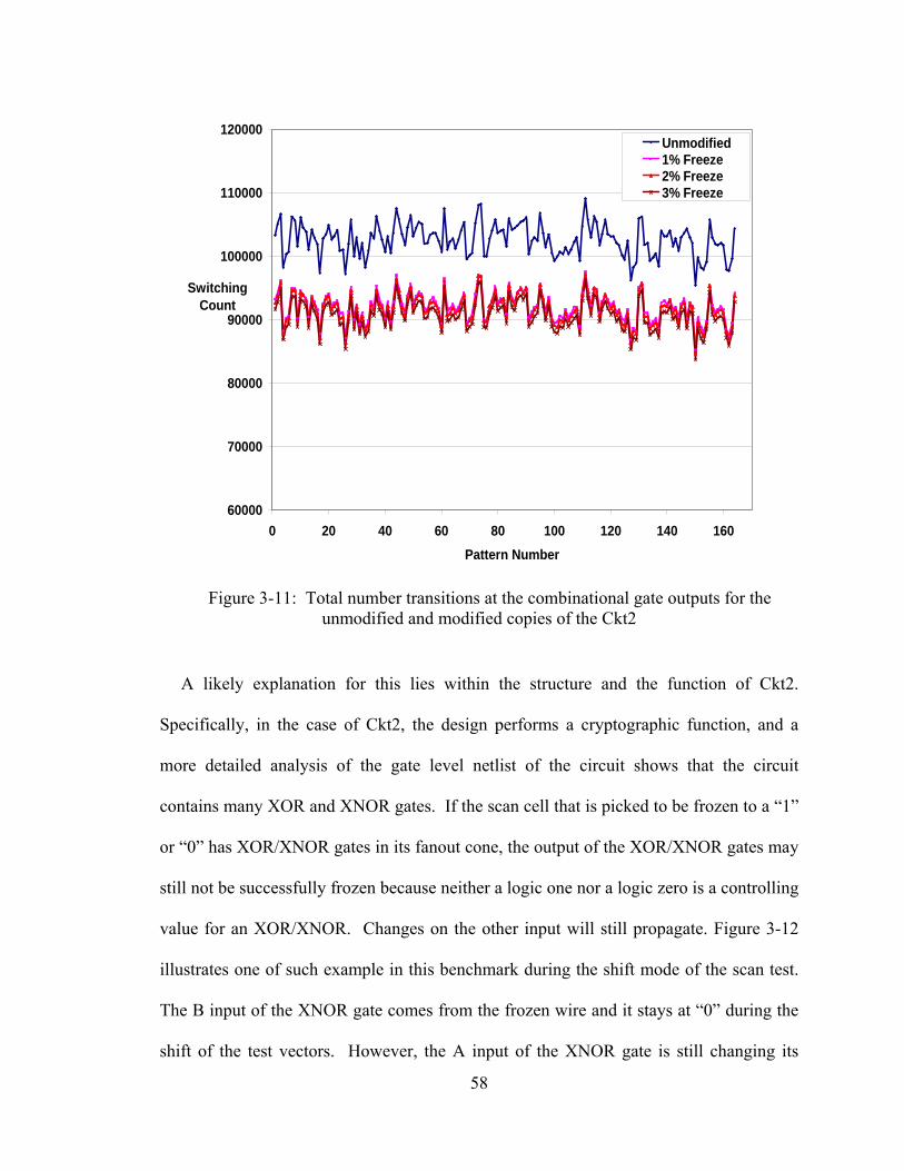
58
60000
70000
80000
90000
100000
110000
120000
0 20 40 60 80 100 120 140 160Pattern Number
Switching Count
Unmodified1% Freeze2% Freeze3% Freeze
Figure 3-11: Total number transitions at the combinational gate outputs for the unmodified and modified copies of the Ckt2
A likely explanation for this lies within the structure and the function of Ckt2.
Specifically, in the case of Ckt2, the design performs a cryptographic function, and a
more detailed analysis of the gate level netlist of the circuit shows that the circuit
contains many XOR and XNOR gates. If the scan cell that is picked to be frozen to a “1”
or “0” has XOR/XNOR gates in its fanout cone, the output of the XOR/XNOR gates may
still not be successfully frozen because neither a logic one nor a logic zero is a controlling
value for an XOR/XNOR. Changes on the other input will still propagate. Figure 3-12
illustrates one of such example in this benchmark during the shift mode of the scan test.
The B input of the XNOR gate comes from the frozen wire and it stays at “0” during the
shift of the test vectors. However, the A input of the XNOR gate is still changing its

59
value, and hence, it causes the output of the XNOR gate to toggle. This suggests that
additional improvements to the power-sensitive scan cell selection procedure (including
the use of an iterative approach) may be possible.
XNOR U970 ( .Z(n1340), .A(\key_r[13]),.B(\inmsg_f[60]) );
B
A
ZB
A
Z
Figure 3-12: Effect of the XOR/XNOR gates to the switching activity reduction
Table 3-4 summarizes the switching activity reduction for all circuits studied. The first
column indicates the circuit name. The rest of the columns show the amount of switching
activity reduction at the combinational gate outputs when 1%, 2% and 3% of the power-
sensitive scan cells are frozen. Note that in each case, the actual number of frozen scan
cells was determined with the following formula:
# of frozen cells = floor (# total_cells * f% +1) 3.4
This ensures, that at least one flip-flop will be frozen in the 1% case even when the total
number of flip-flops in the design is less than 100 (as occurs in Ckt3).
While for all circuits, the switching activity reduction is much larger than the
percentage of the scan cells that are frozen, it is highly circuit-dependent. In some cases,
this is caused by differences in flip-flop observability, circuit functionality, gate types and
the fanout degree fed by flip-flops.

60
Table 3-4
Actual Reduction in Switching Activity at Combinational Part of the Circuit after Freezing Power-Sensitive Scan Cells
Circuit Freeze 1% Freeze 2% Freeze 3%
Ckt1 31% 48% 64%
Ckt2 10.2% 10.6% 11.6%
Ckt3 79% 94% 94%
Ckt4 12% 25% 41%
Ckt5 9.5% 10.5% 11%
Ckt6 5.4% 14.5% 24.3%
Ckt7 7.8% 8.5% 20.4%
Average 22% 30% 38%
For example, extremely high switching activity reduction was obtained with Ckt3.
This is a relatively small circuit, and only a single scan cell was frozen in the 1% case. To
investigate the cause of this dramatic reduction, we analyzed the RTL code and found
that the single frozen signal had a very high degree of fanout. Furthermore, it was often
used as the conditional signal in an if/else statement such that its value determined the
value assigned to another signal. If the frozen signal was set equal to logic 1, the other
signal was assigned a value of 0. If the frozen signal was set to logic 0, then the other
signal was set equal to a value that depended on additional signals in the design.
Obviously, in this case, our algorithm chose to freeze this signal to logic 1, and it implies
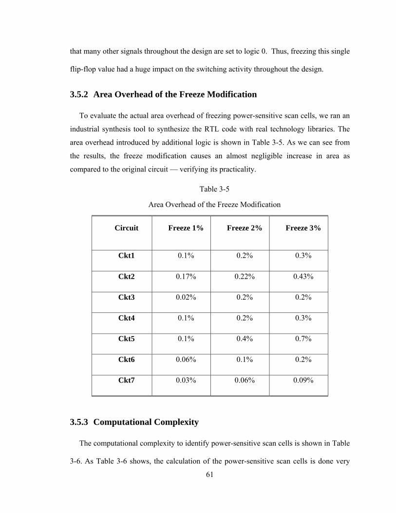
61
that many other signals throughout the design are set to logic 0. Thus, freezing this single
flip-flop value had a huge impact on the switching activity throughout the design.
3.5.2 Area Overhead of the Freeze Modification
To evaluate the actual area overhead of freezing power-sensitive scan cells, we ran an
industrial synthesis tool to synthesize the RTL code with real technology libraries. The
area overhead introduced by additional logic is shown in Table 3-5. As we can see from
the results, the freeze modification causes an almost negligible increase in area as
compared to the original circuit — verifying its practicality.
Table 3-5
Area Overhead of the Freeze Modification
Circuit Freeze 1% Freeze 2% Freeze 3%
Ckt1 0.1% 0.2% 0.3%
Ckt2 0.17% 0.22% 0.43%
Ckt3 0.02% 0.2% 0.2%
Ckt4 0.1% 0.2% 0.3%
Ckt5 0.1% 0.4% 0.7%
Ckt6 0.06% 0.1% 0.2%
Ckt7 0.03% 0.06% 0.09%
3.5.3 Computational Complexity
The computational complexity to identify power-sensitive scan cells is shown in Table
3-6. As Table 3-6 shows, the calculation of the power-sensitive scan cells is done very
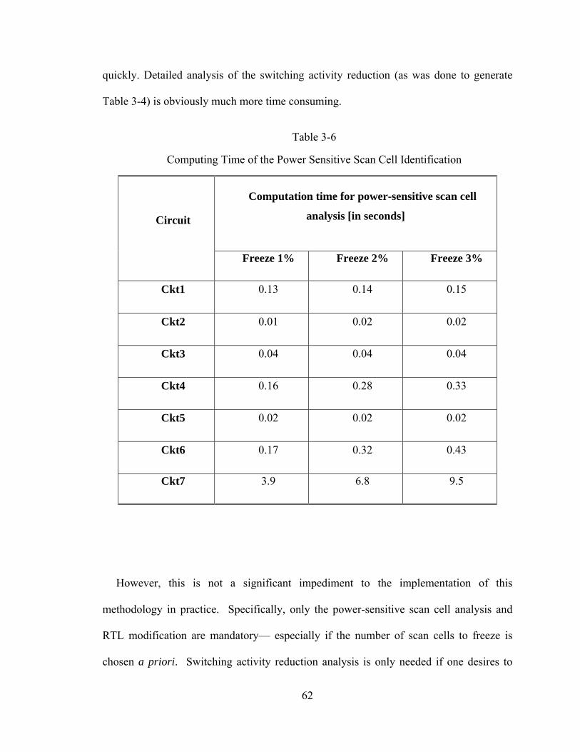
62
quickly. Detailed analysis of the switching activity reduction (as was done to generate
Table 3-4) is obviously much more time consuming.
Table 3-6
Computing Time of the Power Sensitive Scan Cell Identification
Computation time for power-sensitive scan cell
analysis [in seconds] Circuit
Freeze 1% Freeze 2% Freeze 3%
Ckt1 0.13 0.14 0.15
Ckt2 0.01 0.02 0.02
Ckt3 0.04 0.04 0.04
Ckt4 0.16 0.28 0.33
Ckt5 0.02 0.02 0.02
Ckt6 0.17 0.32 0.43
Ckt7 3.9 6.8 9.5
However, this is not a significant impediment to the implementation of this
methodology in practice. Specifically, only the power-sensitive scan cell analysis and
RTL modification are mandatory— especially if the number of scan cells to freeze is
chosen a priori. Switching activity reduction analysis is only needed if one desires to

63
determine the number of scan cells to freeze as a function of the overall reduction.
Furthermore, even in this case, intelligent sampling (such as simulating only an
appropriate subset of all vectors and all shift cycles) will reduce the time required.
3.6 Summary
In this chapter, we have reviewed previous work on low power ATPG and DFT
techniques in the literature. We have presented and analyzed a method for reducing
switching activity during scan shift by freezing a small subset of all flip-flops at the RTL.
We have shown that large reductions in switching activity can be achieved with very low
area overhead. The amount of scan flip-flops that are going to be frozen can be
decreased/increased depending on the design’s overhead budget. In comparison with
previous methods, which freeze these flip-flops at the gate level, timing closure can be
more easily met. When flip-flops are frozen at the gate level, as was done in [63],
individual timing analysis had to be implemented to determine whether or not each flip-
flop could be frozen without violating timing. By freezing all flip-flops simultaneously at
the RTL, we allow the synthesis tool to automatically optimize for timing closure.
In addition, this chapter has presented a detailed analysis of the switching activity
reduction that can be obtained with very few frozen flip flops. In fact, in one case, a 79%
reduction in switching activity was achieved with an area overhead of only 0.02%. This
switching activity analysis considered both hazards and final circuit values.
We also investigated some of the circuit characteristics that led to widely different
degrees of switching activity reduction. Specifically, the switching activity reduction

64
depends upon such factors as the types of gates present within the circuit and the amount
of fanout experienced by each frozen scan cell.
Finally, we also quantitatively investigated the difference in functional and test
switching activity for a benchmark circuit with a well-defined function. For the
combinational logic, the switching activity during the scan and capture cycles of the test
was 2.3 and 4.75 times the functional switching activity respectively. For this circuit,
functional switching activity could be obtained during scan shift with our method by
freezing between 2% and 3% of all scan flip-flops.

65
Chapter 4
Unexpected Timing in Silicon
With the reduction in feature and interconnect sizes that occurs with device scaling,
the timing and performance of today’s designs has become very sensitive to deep
submicron (DSM) effects, such as local and global variability, static and dynamic IR
drop, and temperature gradients. Such effects are often not well-modeled in timing
analysis tools. As a result, reducing the timing discrepancy between design simulation
and silicon measurement has become a major challenge of current VLSI technology. In
fact, post-silicon timing validation is one of the most time-consuming and challenging
phases of the silicon debug process [67].
For example, the authors of [68] emphasize the necessity for closing the gap between
the timing observed in the pre-silicon simulation and post-silicon validation phases. They
have highlighted the need for improving the pre-silicon tools and methodologies in order
to make better predictions of the behavior of the design [68]. However, despite the
development of powerful and enhanced simulation techniques for the pre-silicon phase,

66
mismatches in the circuit’s behavior still occur between the simulated design and on
silicon.
The timing mismatches between the silicon and simulation are important because they
make it hard to accurately design circuits that meet timing specifications at first-silicon.
Furthermore, in addition to the difficulty they have in accurately predicting the actual
path delays, current static timing analysis tools also may have difficulty in finding the
real speed-limiting paths of circuits. Such information is needed to be able to optimize
the performance of high-performance designs. For example, the delay of a critical path
can be shortened by replacing some of the high-Vt cells with low-Vt cells. Thus, the
timing discrepancy between design simulation and silicon measurement is one of the
major problems which requires additional attention during the pre-silicon simulation and
modeling phase.
In this chapter, we propose a noise index model, NIM, which can be used to predict the
mismatch between expected and real path delays that arises due to switching and IR-drop.
The noise index considers both the proximity of switching activity to the path and
physical characteristics of the design. To evaluate the method, we performed silicon
measurements on randomly selected paths from an industrial 65nm design and compared
these with Spice simulations. We show that a very strong correlation exists between the
noise index model and the deviations between simulations and silicon measurements.
We will first review related previous work on the timing mismatches between silicon
and simulation problem. Then we will introduce our Noise Index Model, which can be

67
calculated and used inexpensively to predict the magnitude of these timing mismatches
between the real delays on silicon and the estimated delay values from simulation.
4.1 Delay Discrepancies between Silicon and Simulation
The interaction between pre-silicon design simulation and post-silicon measurement
has been widely studied in the literature. In this section of the dissertation, we will review
some of the previous work related to this problem.
The authors of [69] provide a detailed description and analysis of the potential effects
leading to unexpected timing behavior in silicon. According to [69], the unpredictable
silicon behavior can be caused by topological effects, where the problem arises due to the
location and/or orientation of the cells; static effects, which are mostly related to the mis-
modeling of the cells; statistical effects, which covers the intra-die and inter-die process
variations; random effects, which considers any effects that are not based on a statistical
system; and dynamic effects, which are dependent of the applied input patterns and cover
the issues like cross coupling noise, dI/dt voltage drop, IR-drop and etc..
Previous work [70] [71] applies the statistical data learning methodology to identify
the most important effects that lead to unpredicted timing behavior of the final silicon. In
[70] and [71], the authors analyze and diagnose the cause of the mismatch in the path
delays between the predicted results and the measurements on silicon. To be able to
diagnose the unexpected timing behavior, the authors of [70] and [71] describe each path
with a collection of potential causes of the timing discrepancy. Then a statistical data
learning process is applied to rank the importance of every cause leading to the timing
mismatch between design and silicon.

68
The authors of [72] use the same framework as in [70] and [71] to form the optimal set
of the paths that need to be measured on the silicon such that the unexpected timing
effects are effectively analyzed. In [73], the authors introduce a method where they
identify a small set of representative speed-limiting paths which are more prone to fail
during the post silicon timing validation stage. They insert extra test logic in the original
design in order to calculate the delay of the representative paths during the design stage
and use the delay values of the representative paths to predict the timing of the real
silicon. In [73], only process variations are considered as the source of the delay
uncertainty on silicon; other effects are not considered in this work. The authors of [74]
present a rule learning based data mining methodology for analyzing the timing critical
paths from actual AC delay measurements on silicon.
In [75], a representative critical path synthesis approach that increases the correlation
between the predicted and measured delays is introduced. Extra on-chip test structures,
which will capture the effects of process variations on all critical paths, are inserted into
the original circuit. The on-chip test structure is also used to measure the delay of the
critical path. The main issue in [75] is to come up with a reliable method for synthesizing
the test structure such that it will give a reliable delay prediction of the silicon under
process variations.
In addition to data mining techniques which focus on the main causes of the timing
discrepancies, other researchers have developed detailed power supply analysis [76-81]
and maximum instantaneous power/current estimation [82-86] techniques. These
methods rely on costly RLC network analysis and simulation. These methods usually use
a simplified RLC circuit in order to model the power supply network and perform a

69
SPICE simulation to characterize the current and voltage waveforms of the cells in the
design.
As an alternative to the past research on detailed power supply noise analysis and
maximum instantaneous power/current estimation techniques, we have developed a
correction model, the noise index model (NIM). This model can be used to inexpensively
estimate a correction factor that can be applied to the path delay prediction of a
commercial tool. Unlike the previous work described in [69-72, 74] that ranks all the
potential causes leading to the timing discrepancy between design simulation and silicon,
this paper focuses specifically on the effect of the switching activity-generated IR-drop
on the actual delay of the circuit paths and estimates the magnitude of the timing
discrepancy. The next section of this chapter focuses on the details of the noise index
model.
4.2 Path Delay Measurements vs SPICE-Level Timing
Analysis
The first step in this investigation involved determining the correlation between
predicted delays obtained from SPICE-level timing analysis and measured delays on
silicon. In this dissertation, path delay test patterns are used to measure the signal
propagation time along a well-defined circuit path on an industrial design that is
manufactured with a 65nm process technology for multiple circuit instances. Note that it
is not our intention to reproduce application conditions, but to obtain a well-defined

70
environment for our delay measurements. These measured delays of the circuits’ paths
are then compared with the SPICE-level timing analysis.
One of the major limitations of the path delay fault model is that the number of the
paths in a design grows exponentially with circuit size. Therefore a proper selection of
the circuit paths for investigation is required. The current path selection method for this
experiment is based on the timing report of an industrial static timing analysis (STA)
tool. A very large number of paths with a wide range of delays are targeted in this
experiment. The selected paths are given as an input to an in-house ATPG tool in order
to create hazard-free robust launch-on-capture (LOC) path delay test vectors.
The path delay test patterns are applied on the test system with subsequent faster
timings to determine the delay of each path. These measurements were made on over a
hundred typical devices for 900 paths at an ambient temperature of 25°C and a nominal
supply voltage of 1.2V. The typical accuracy of these measurements is 10 ps. To remove
the effects of local process variations, the results are normalized over all devices. These
normalized delays are compared with SPICE-level timing analysis. Since it is infeasible
to perform SPICE-level analysis on the whole circuit, we use extracted paths, including
all side inputs and the state of these side inputs during path delay measurements in
SPICE. The comparison between the predicted path delays and the measured path delays
is shown in the correlation plot in Figure 4-1.
Every dot in Figure 4-1 corresponds to a different path of the design. Any path
located beneath the 45 degree line has a real delay that is more than the expected delay;
hence the design will be slower on silicon for that path. On the other hand, any path

71
located above the line has a real delay that is less than the expected delay. The three
outliers corresponding to the paths A, B and C are chosen from the slower than expected
and the faster than expected group in Figure 1. The detailed investigation of the switching
activity regarding these paths will be shown shortly.
PATH B
PATH C
PATH A
PATH B
PATH C
PATH A
Figure 4-1: Correlation between expected and measured path delays
As one can observe in Figure 1 we have discrepancies on the order of -75 to +75 ps or
+/- 5%. These discrepancies are well above our measurement inaccuracies and can be
caused by various factors. However, the setup of the experiment ensures that several of
these factors are strongly reduced:

72
• Local process variation is reduced by the normalization of the measurements.
• Global process variation is reduced by having ‘typical’ silicon and again the
normalization process.
• Static IR-drop is reduced by the path-delay measurement setup in which
measurements are performed after a quiescent period in which the supply voltage is
restored.
• Clock jitter is reduced by measuring each path under very similar external clock
conditions. Hence, there is a well defined clock input signal of the test system.
One of the major remaining factors is the switching activity around the specified paths.
Switching activity and the associated dynamic IR drop are some of the harder to grasp
effects for EDA tools. The actual impact is pattern specific; however it is infeasible to
evaluate all state switching possibilities. Hence, for practical purposes, tools generally
need to rely on some vector-less analysis. Unfortunately, the vector-less analyses are
inaccurate because they rely on uniform switching probability of the circuit nets. Here we
investigate the amount of switching activity and the switching activity profile of the circuit
for the launch cycle of the applied path delay test pattern for a certain number of selected
paths.
For example, consider
Figure 4-2. The switching activity profile of the circuit for two selected paths, path A
and path B is shown in
Figure 4-2. In

73
Figure 4-2, red indicates active areas and blue indicates the quiescent areas of the chip.
The black circles in
Figure 4-2 represent the location of the two paths. Path A, which is slower in silicon, is
located in a highly active area as compared to path B which is faster in silicon.
Furthermore, in addition to the highly active switching area in the vicinity of path A, the
upper left corner of the circuit is also very active for this path delay pattern.
Path A slower on Si Path B faster on SiPath A slower on Si Path B faster on Si
Figure 4-2: Switching activity profile of two different paths at launch cycle
One could argue that the slowness of path A is a result of both the local and global
switching activity on the circuit. However, a further investigation of the switching

74
activity shows that a path may be slower than expected even when the global switching
activity in the circuit is unremarkable. In Figure 4-3, the circuit’s switching activity
profile for two slower than expected paths is shown. As we can see from Figure 4-3, path
C, which belongs to the slower than expected group, does not have any significant global
switching activity as occurs in the case of path A.
Path A slower on Si Path C slower on SiPath A slower on Si Path C slower on Si
Figure 4-3: Switching activity profile of two slower than expected paths at launch cycle

75
This switching activity profile analysis was also performed for a number of other
paths. Observations from the switching activity analysis showed that for the slower than
expected paths, the switching activity around the paths is much higher than the switching
activity around the faster than expected paths. With these observations, we developed a
new noise index model that considers the effects of the switching activity in the vicinity
of a path on its actual delay without requiring detailed analysis of the design.
4.3 The Noise Index Model
The noise index model attempts to efficiently capture the decreasing importance of the
switching activity surrounding a path as the distance from the path increases. For
example, consider Figure 4-4. In Figure 4-4, the purple triangles represent the instances
belonging to the path, and the red circles represent the switching instances in the vicinity
of the path. An instance of the path may be either the launch/capture flip-flop or one of
the combinational gates connecting the launch and capture flip-flops along the path. The
dotted black ellipses around every instance indicate the neighboring region that is used
for the noise index calculation.
The radius of the ellipses in both the x- and y- directions is calculated based upon
decoupling capacitance analysis. Decoupling capacitance has been studied
comprehensively in the literature, and effective decoupling capacitance placement plays a
significant role in the current VLSI technology [87-93]. Decoupling capacitors are used
to manage the power supply noise of the design. In general, an SoC is made of building
blocks where each of these blocks consists of rows of standard cells [87]. Switching of a

76
cell in the design basically charges and discharges the capacitances for the corresponding
node.
The switching of a cell initiates a current and leads to a voltage drop and spike at the
power and ground lines of the circuit. The voltage drop is initially restored from the
locally available decoupling of the neighbor cells before it is restored from the power
supply network. The decoupling cells can be either the non-switching cells that are in the
vicinity of the switching cells or they can be additionally inserted decoupling cells. When
the decoupling capacitances are inserted additionally into the design; there are two
important challenges that need to be taken into account: the location of the decoupling
capacitance and the size of the decoupling capacitance. We will use the former
parameter; the effective location of a decoupling capacitance, as a basis in our noise
index model because switching activity induced dynamic IR-drop plays a significant role
in both of the decoupling capacitance and noise index analyses.
As we will show later, the decoupling radius equation depends on the sheet resistivity
of the metal layers in the power grid. The sheet resistivity of the horizontal and vertical
metal layers of the power grid may be different depending on the design of the power
grid. As a result, the decoupling radii in the x- and y-directions may be different, leading
to an elliptical shape as is shown in Figure 4-4. If the power grid has horizontal and
vertical metal layers with identical sheet resistivity, then the resulting shape will be a
circle instead of an ellipse.

77
Instance belonging to the pathSwitching neighbor instanceInstance belonging to the pathSwitching neighbor instance
Figure 4-4: Switching activity area of interest for the noise index model
In [88] a model was proposed for the calculation of the effective radius of on-chip
decoupling capacitors. In [88] it was also shown that beyond this distance the decoupling
capacitances become ineffective. The differential equation in [88] can be solved to
calculate a voltage drop profile by assuming a current profile for the switching instance
under investigation. Here a triangular shaped current source is applied with a switch
duration Ts and a switched capacitance Cs, resulting in a max current Imax as shown in
Figure 4-5. The switch duration of the triangular pulse is taken as 30 ps.

78
Figure 4-5: Triangular shaped current profile
The voltage drop profile for the moment of the maximum current is derived in [87]
and is given by:
⎥⎥⎦
⎤
⎢⎢⎣
⎡⎟⎟⎠
⎞⎜⎜⎝
⎛−⎟
⎟⎠
⎞⎜⎜⎝
⎛=
s
usq
s
usq
s
sqs
TrcR
TrcR
TRCV
rv2
E2
E2
)(2
2
2
1sup
π 4.1
where Vsup is the supply voltage, Rsq is the effective resistivity of the metal layers of the
power grid, and Cu is the capacitance per unit area of the power grid of the SoC. The E1
and E2 functions are exponential integrals of the order 1 and 2 respectively. Note that in
Equation 4.1 when the radius is equal to 0 (at r=0) v(r) goes to infinity. This is due to the
model having a single point where the current source is connected. Therefore the
equation is observed here at a realistic radius r0, for example at a value of the rail distance

79
from the power supply of the standard cells. The voltage drop profile is obtained by
scaling of the voltage drop:
)(/)()(' 0rvrvrv = 4.2
An example of a voltage drop profile versus radius is shown in Figure 4-6. Note that
the voltage drop v`(r) is dimensionless because of the scaling with respect to r0.
Figure 4-6: Voltage drop profile vs radius
The radius rd in Figure 4-6 denotes the decoupling capacitance radius derived in [87]
and can be calculated from
usq
sd cR
Tr 2.1= 4.3

80
The decoupling radius rd defines the boundaries for the noise index calculation for
every instance belonging to the path under investigation. Any switching instance located
at a distance larger than rd from the path instance is beyond the scope of the noise index
model and can be neglected. Once the neighborhood region is defined, the noise index
model sums the weighted switching activity of the cells within each region for the launch
cycle of the path delay test pattern. Here, the weight assignment for the noise index
calculation is determined by the drive strength of the output stage of the switching
standard cells. In addition, the importance of a neighboring switching standard cell within
the ellipse is determined by its distance from the path instance. For a given path instance
under investigation, the effect of the neighboring switching instances is scaled depending
on the distance of the switching instance to the path instance. To consider the differences,
three other ellipses are formed around the path instance by considering the voltage drop
profile inside the larger ellipse with the radius of rd. The voltage drop profile along rd is
calculated from Equations 4.1 and 4.2.
From Figure 4-6, we calculated the boundaries for the other three ellipses. The effect
of the switching cells falling into the blue region that is located closest to the actual path
instance was given a full weight of 100%. The effect of the switching cells falling into
the green region, which is second closest ellipse to the actual path, was scaled by 75%,
and so on.
Thus, the NIM value for a path instance i can be computed as:
j
cellsgneighborin#
jji SWSANIM ∗= ∑
=1 4.4

81
where the neighboring switching cells are those within the largest ellipse surrounding
instance i, and WSAj is equal to the weighted switching activity of neighboring switching
cell j. This is multiplied by the scaling factor Sj which is equal to 1, 0.75, 0.5, or 0.25
depending on the location of neighboring switching cell j.
Once the NIM value of each path instance is found, the sum can be taken—yielding a
single NIM value for that path.
∑=
=cesinspath
iipath NIMNIM
tan#
1 4.5
The goal is to then use this NIM value to estimate the difference between the true and
predicted path delay.
4.4 Flow for the Noise Index Model
The flow for the noise index and switching activity profile analysis is shown in Figure
4-7. First, path delay test patterns are created with an in-house ATPG tool and then
simulated with a commercial simulator. The timing information for the netlist is included
in the simulation, and hence the effect of the non-functional transitions (i.e. hazards) in
addition to the functional transitions is considered in the switching activity investigation.
From this simulation, a VCD file is generated for the launch clock cycle of the path delay
test vectors. A DEF file describing the location of the standard cells is generated with a
commercial layout tool. The noise index analysis program parses the VCD and the DEF
files for the spatial analysis of the switching activity in the neighborhood of the paths and

82
calculates the noise index of the paths. The noise index analysis program also generates
an output file where the switching activity profile of the design under an applied input
pattern can be visualized.
VCD
DEF
Path Delay Test Vectors
Noise Index Analysis
VCD
DEF
Path Delay Test Vectors
Noise Index Analysis
Figure 4-7: Flow for the noise index analysis
4.5 Correlation between NIM and Delay Difference between
Design Simulation and Silicon
In this section we show the effectiveness of our noise index model. We validated the
effectiveness of the noise index model for predicting delay differences between silicon
and simulation. This analysis was performed for a number of paths belonging to both the
faster and slower than expected groups. The noise index values were calculated with the
proposed flow that is described in the former section. The correlation between the paths’
noise indexes and the differences between the simulated and measured path delays is

83
shown in Figure 4-8. The x-axis of the plot in Figure 4-8 represents the noise index
values of the selected paths, and the y-axis of the graph shows the difference between
SPICE-level timing simulation delay and the measured averaged delay values. As we can
observe from Figure 4-8, the paths that are slower in the silicon tend to have higher noise
index values than the paths that are faster in silicon. The 0.87 correlation coefficient
shows that the noise index of the paths and the delay difference of these paths are highly
correlated.
R2 = 0.87
-0.1
-0.08
-0.06
-0.04
-0.02
0
0.02
0.04
0 200000 400000 600000 800000Noise Index
Del
ay d
iffer
ence
bet
wee
n si
mul
atio
n an
d m
easu
rem
ents
[ns]
Figure 4-8: Delay difference vs. noise index values

84
4.6 Summary
In this chapter, we reviewed some of the previous work that has been done to solve the
problem of the timing discrepancy between silicon and simulation. We performed a
detailed investigation of the switching activity for an industrial design when path delay
test vectors are applied. A noise index model is developed to characterize the timing
discrepancy between silicon measurements and simulation predictions as a function of
switching activity and IR-drop. The delays of a number of selected paths are measured
on silicon under typical conditions and compared with the delays of the same paths as
predicted with SPICE-level simulations.
The proposed noise index model has several potential applications even earlier in the
design process where exact measurements of the delay difference are less important. For
example, in the design phase, the NIM can be used to identify candidate locations for the
insertion of decoupling capacitance. In addition, the current path selection algorithms for
test and validation, which usually rely on the timing report of the STA tools, can be
improved by using the noise index model. Finally the NIM can be used to generate test
vectors that can mimic the worst case functional switching activity during test. In the next
chapter we will show how we used the NIM to fill a subset of the don’t care bits of a test
cube such that the worst case functional switching activity around critical paths can be
replicated during the test.

85
Chapter 5
High-quality At-speed Testing
With the latest advances in VLSI technology, power supply switching noise has
become a critical issue during high-quality at-speed testing. It has been shown that the
discrepancies between the circuit’s switching activity during its functional and test mode
can cause over-testing problems and lead to yield loss. Alternatively, reduced power
supply noise effects around critical paths can actually result in under-testing of the chip,
causing test escapes. In order to achieve a high-quality at-speed test, it is mandatory to
solve both the over-testing and under-testing problems simultaneously. In chapter 4, we
introduced our previous work developing the noise index model, NIM, which can be used
to predict the mismatches between expected and real path delays. The noise index model
(NIM) presents a new way of characterizing the magnitude of the timing mismatch
between silicon and simulation based upon the switching activity in a well-defined area
around the path.

86
In this chapter we quantitatively investigate and compare the noise index values for
the critical paths during functional and test modes. We perform a detailed investigation of
the switching activity in functional mode and relate that switching activity to the area
around the path of interest. Our analysis shows that the total amount of the switching
activity and the locality of this switching activity during functional mode exhibit large
variations depending on the clock cycle of interest. To reduce our chances of either over-
testing or under-testing the circuit, these variations must be considered during test
generation. We then propose a test pattern modification method that harnesses the noise
index model. The proposed method takes the partially specified test vectors and fills a
subset of the don’t care bits in the test vectors such that the worst observed functional
noise index for the targeted critical path will be replicated during test mode.
Our proposed test pattern modification technique will intelligently fill the don’t cares
in launch-on-capture (LOC) path delay test patterns. Specifically, we will simulate
characteristic functional inputs and identify the clock cycles with greatest activity in each
subset of the circuit. We then fill a subset of the X’s in each path delay test pattern to
replicate the worst case functional switching activity profile in the NIM-identified region
around a given path. We will demonstrate that we can achieve a high correlation between
the switching activity for the maximum simulated functional and test modes of operation.
In this chapter we will first review the previous work that has been done in this area
and then present a detailed quantitative analysis of a circuit’s switching activity during
functional and test modes of operation. Then we will describe our NIM-based X-filling
algorithm. With the proposed flow, the NIM difference of the path between test and

87
functional mode will be minimized and hence the circuit will be tested as closely as
possible to its functional mode for each path under investigation.
5.1 High-quality Test Pattern Generation and Manipulation
Techniques
The effect of the excessive switching activity during at-speed scan testing becomes
especially important when the aim of the test is to detect timing-related faults. The basic
contributors for the delay of a path are: nominal path delay, defect-induced path delay
and power-supply-noise-induced delay [17]. As we have already stated, power supply
noise induced by excessive switching activity during at-speed scan test can cause
performance related problems and even yield loss. Therefore, power supply switching
noise has become an important factor for delay fault testing.
Recently, several approaches have been proposed to minimize the power supply noise
effects during at-speed testing. For example, pseudo-functional testing has gained a lot
of interest in recent years. The goal is to generate tests that reduce the discrepancies in a
circuit’s switching activity between its functional and test modes. Many techniques for
generating pseudo-functional, also known as functional-like, patterns have been proposed
in literature [94-98]. In addition to the pseudo-functional tests, other ATPG-based
solutions explicitly attempt to reduce the power dissipation and power supply noise
effects during at-speed delay test. We have reviewed some of these power-aware ATPG-
based techniques in Chapter 3. In this section we will only review the ATPG-based

88
techniques which incorporate the power supply switching noise effects when creating the
delay test patterns.
5.1.1 Pseudo-Functional Test
The essence of pseudo-functional testing is to identify functionally unreachable and
illegal states of the circuit, and to generate test sets that avoid the extracted illegal states
[94]. The pseudo-functional test reduces the possibility of yield loss, because, with the
avoidance of the non-functional states, the circuit is expected to operate as closely as
possible to its functional mode. The major concern of pseudo-functional testing is illegal
state identification. The quality of the pseudo-functional test set heavily depends on the
completeness of the identified illegal states.
Researchers have proposed different techniques for illegal state identification for
pseudo-functional testing. In [94], authors extract the illegal states of the circuits based
upon a topological partial reachability analysis of the design and the results from a
sequential SAT solver. Authors in [95] use indirect implications from static learning for
identification of the illegal states, which are later used to direct the test pattern generator
such that the patterns will contain as few illegal states as possible. The search space of
the illegal state extraction problem is reduced in [96] by analyzing only the multi-fanout
nets, which are known to be the root cause of the illegal states in a circuit. A
compression-aware pseudo-functional testing technique is proposed in [99], where
instead of activating all functional constraints, only relevant functional constraints are
activated for the targeted fault. Therefore, the generated patterns will be compression-
friendly because they will have a lower percentage of specified bits. The authors of [100]
generate pseudo-functional patterns by extracting some functionally-reachable states

89
around critical paths and feeding them into the ATPG tool. An X-filling algorithm is then
performed on the pseudo-functional patterns in order to maximize the PSN effects around
the critical paths. In [97], broadside test patterns are concatenated to form multi-cycle
scan tests. Multi-cycle scan test is performed by the consecutive application of several
primary input patterns between scan operations; during this time, the circuit is expected
to operate in a manner close to its functional mode. In [98], the authors propose an ATPG
scheme which can be integrated with an embedded deterministic test, EDT, environment
for reducing the switching activity during the capture cycles of the scan test. The
reduction in switching activity is achieved by using a pseudo-functional pattern in order
to initialize the circuit and then applying the test cube to the circuit under test.
5.1.2 Power Supply Noise Aware Pattern Generation
In addition to these pseudo-functional tests, other ATPG-based solutions explicitly
take into account the power supply noise effects on the delay of the circuit. We have
already reviewed the previous research on how to reduce the switching activity during
scan-based test mode. In this section, we will review previous work on minimizing the
power supply noise effects on delay testing.
In [80] and [101], a power model is developed to estimate the power supply effects in
the circuit; then the power model is used to compact the test patterns such that PSN is
evenly distributed among all the patterns and such that it is below the given budget. The
authors of [44] first perform a power supply network analysis to create a threshold
matrix. The threshold matrix is determined by focusing on the number of gates in each

90
cell of the threshold matrix and the average functional switching activity of the design. A
test compaction algorithm is performed to match the switching matrix of the delay
patterns with the threshold matrix. The authors of [43] present a pattern validation
technique using a weighted switching activity metric. Another pattern grading technique
using an output deviation metric is proposed in [39]. Finally, another pattern selection
method is presented [38]. The test patterns are selected such that the overlap of the
sensitized paths between patterns is kept as small as possible.
Unlike earlier work that relies on illegal state identification, the vector-less analysis of
the circuit, or a designer-specified switching activity percentage for functional mode
switching activity calculations, we take into account the actual functional switching
activity of the circuit for the specific clock cycles of interest. The next section presents a
detailed analysis of a circuit’s switching activity that includes incorporating the layout
information of the circuit.
5.2 Noise Index Analysis for Functional and Test Modes
In Chapter 3, we presented a quantitative analysis on the nature of the switching
activity for a circuit during functional and test modes. The average number of transitions
of the circuit during the scan shift and capture cycles was compared to the average
number of transitions of the circuit during functional mode clock cycles. The switching
activity analysis that was presented in Chapter 3 was based on the counting of the
switching of all the standard cells’ outputs and comparing the counts between test and

91
functional modes. The physical locality of the switching cells inside the circuit was not
studied.
In this section, we extend our switching activity analysis by incorporating the layout
information of the circuit. The overall flow for the switching activity analysis is shown in
Figure 5-1.
RTL libraries
Synthesis + Scan-Insertion Tool
Netlist
Layout Tool
DEF
STA SDF
Critical paths
Scan Inserted Netlist
ATPG Tool
PDF Test Vectors
VCS
VCD
RTL libraries
Synthesis + Scan-Insertion Tool
Netlist
Layout Tool
DEF
STASTA SDFSDF
Critical pathsCritical paths
Scan Inserted Netlist
ATPG ToolATPG Tool
PDF Test Vectors PDF Test Vectors
VCSVCS
VCDVCD
Figure 5-1: Flow for VCD and DEF files generation

92
An RTL description of the circuit is synthesized with 90nm technology libraries in
order to obtain the gate level netlist. Robustly detected path delay test vectors with a LOC
clocking scheme are generated with TetraMAXTM (Synopsys). Synopsys’s static timing
analysis tool Primetime is used to generate the critical paths of the circuit. The generated
test patterns are simulated on a gate level netlist with the VCS logic simulator. The timing
information for the netlist is included in the simulation through a standard delay format
(SDF) file. Using the SDF data in the logic simulation enabled us to consider the effect of
the non-functional transitions (i.e. hazards) in addition to the functional transitions in our
switching activity investigation. From the gate level netlist simulation, Value Change
Dump (VCD) files are generated for functional and test modes. A Design Exchange
Format (DEF) file is generated with the Synopsys’s IC-Compiler layout tool and then
parsed for the physical location analysis. The VCD and DEF files are later processed by a
script developed in-house to analyze the distribution of the switching activity for all the
gates over any specified time slot.
The example circuits for the NIM investigation are benchmark circuits obtained from
opencores.org [64]. The first circuit under investigation is the color converter benchmark,
which we used in our previous switching activity analysis. The second circuit for the NIM
investigation is a floating point unit (FPU) benchmark. The FPU was tested with test
cases that were created by the designer using SoftFloat software [102].
We first simulated the circuits in functional mode and collected the switching activity
data for functional inputs. The maximum number of transitions at any clock cycle and the
average number of transitions per clock cycle at the standard cells’ outputs for functional
simulation are shown in Table 5-1.

93
Next, we collected the switching activity information for path delay test patterns
during the launch clock cycle for different types of don’t care bit filling options. We
utilized the different don’t care bit filling options that are provided by the ATPG tool. We
generated the test sets with four different types of X-filling options: a No-Fill test set,
where the don’t care bits are left as X’s; a 1-Fill test set, where all the don’t care bits are
filled with logic 1; a 0-Fill test set, where all the don’t care bits are filled with logic 0,
and finally a Random-Fill test set, where the don’t care bits are filled randomly.
Table 5-1
Average and Maximum Number of Transitions during Functional Operation
Average Maximum
Color Conv. 1394 3491
FPU 2085 6811
Specifically, we analyzed the switching profile of the test patterns for the four
different cases. The average number of transitions at the outputs of the standard cells per
test pattern is shown in Table 5-2. The total number of transitions are counted for every
test pattern of the test set and then averaged over the total number of test vectors in the
test set. Any switching from an X value to any another value is counted as 0.5 switching.
From Table 5-2 we can see that when the don’t care bits are filled with the three different
techniques that the switching activity increases dramatically.

94
The discrepancies of the circuit’s switching activity between its functional and test
modes can be seen from Table 5-1 and Table 5-2. Comparing the switching activity
between Table 5-1 and Table 5-2, it can be seen that the patterns without any X-filling
result in very low switching activity compared to the functional case; on the other hand,
when we utilize each of the different types of X-filling options the average number of
transitions is very high compared to the functional mode Specifically the average number
of transitions during functional mode is 16 times larger than the average number of
transitions for the No-Fill test set. On the other hand, for the other X-filling options the
average number of transitions during functional mode is 4.1, 3.8 and 3.9 times less than
the average number of transitions for the Random, 1-Fill and 0-Fill test sets respectively.
Table 5-2
Average Number of Transition during Path Delay Test Mode
The overall switching activity comparison between the functional and test modes is a
good place to start to analyze the circuit’s behavior during its different modes of
operation. However, optimally reducing the effects of power supply switching noise on
path delay test vectors requires a more detailed spatial analysis of the switching cells and
their physical proximity to the targeted critical paths. Previously, many X-filling
No-Fill Random-Fill 1-Fill 0-Fill
Color Conv. 87 5730 5414 5445
FPU 126 11340 10524 10231

95
techniques have been presented to reduce the overall switching activity of the circuit.
However reducing the circuit’s overall switching activity might not adequately reduce
PSSN effects. The noise index model described in Chapter 4 showed that the physical
closeness of the switching cells to the targeted path plays an important role in
determining the effect of the switching cells on the delay of that path. High-quality path
delay test patterns should match the switching activity profile around the critical paths to
the worst case functional activity profile. To accomplish this, our X-filling algorithm
aims to match the NIM value of a path during test mode with the worst case functional
NIM value. However, to find a good estimate for the worst case functional NIM, we need
to decide which functional clock cycle should be used for functional NIM calculations.
Then the question becomes: How do we know which functional clock cycle to pick in
order to match the NIM of the path? The naive approach would be to pick the clock cycle
when the circuit has the overall maximum number of transitions. However, the functional
clock cycle when the overall circuit has its maximum number of transitions might not
give the worst case switching activity profile for a particular critical path.
Alternatively, we could record the average number of switches for every gate
individually during the entire functional simulation and calculate the functional NIM
using the average number of transitions of the standard cells in the NIM area around a
path. However, calculating the functional NIM based on the average number of
transitions for every gate wouldn’t necessarily replicate the worst case switching activity
scenario for the critical paths either. Thus, instead of looking at the global switching
activity of the circuit, we performed a regional local activity analysis to find the actual

96
maximum functional switching activity around the critical path for a characteristic set of
functional patterns.
For a detailed local switching activity analysis, the circuit is divided into smaller
regions. The switching activity profile is then analyzed for each small region during the
circuit’s functional simulation. For example, consider Figure 5-2. where the blue dots
represent all the instances belonging to robustly detected critical paths for the color
converter circuit. In addition to the location of the path instances, the red dotted lines in
Figure 5-2 also show the borders for different regions inside the circuit. In Figure 5-2,
each region is represented by four numbers. The first number, which indicates the region
number, is followed by the second number, which is the maximum number of transitions
on any clock cycle occurring inside the region for the whole functional simulation. The
third number represents the average number of transitions per clock cycle inside the
region during the functional simulation. Finally the fourth number in the second line of
each region indicates the clock cycle where the corresponding region has its maximum
number of transitions. One should note that for each region, the maximum number of
transitions during the functional simulation happens at a different clock cycle. Depending
on the location of the critical path, the noise index of the path during test mode will be
matched to the noise index of the path during functional mode for the clock cycle when
the region of interest has its maximum transition count. For the first benchmark, all the
robustly detected critical paths are clustered in the lower corner of the circuit, so we only
need to consider regions 8, 10, 11 and 12.

97
0 0.5 1 1.5 2 2.5 3x 10⁵
0
0.5
1
1.5
2
2.5
3 x 10⁵
X-Coordinate
Y-C
oord
inat
e
1 – 286, 79
25411
4 – 189, 80
21119
2 – 356, 97
18414
3 – 255, 91
4677
5 – 450, 150
8118
6 – 506, 167
19550
7 – 214, 167
3329
8 - 207, 76
19550
9 – 742, 227
19780
12- 268, 114
26198
11- 323, 135
1206710 – 284, 101
14833
1 – 286, 79
25411
4 – 189, 80
21119
2 – 356, 97
18414
3 – 255, 91
4677
5 – 450, 150
8118
6 – 506, 167
19550
7 – 214, 167
3329
8 - 207, 76
19550
9 – 742, 227
19780
12- 268, 114
26198
11- 323, 135
1206710 – 284, 101
14833
Figure 5-2: Location of the robustly-detected critical paths for color converter and the regions of the circuit with average and maximum
functional switching activity
Similarly, the FPU benchmark is divided into smaller regions, and each region is
analyzed in terms of its switching activity profile. The FPU benchmark has 16 regions
because it is a larger design than the color converter benchmark. Once again, we
performed the spatial switching activity analysis for all of the regions. The spatial
switching activity plots are obtained with a script which is implemented in MATLAB. In
Figure 5-3, Figure 5-4 and Figure 5-5, we show three switching activity profiles for three

98
different regions at different clock cycles when the particular region has its maximum
number of transitions. The black dotted circles in these figures represent the rough
location of the regions inside the circuit. Figure 5-3 shows the switching activity profile
for the functional clock cycle when region 1 has its maximum switching activity.
Figure 5-3: Spatial activity profile for region 1
As we can see from Figure 5-3, a hot spot (where hot refers to switching activity and not
temperature) is located in the upper left corner of the circuit where region 1 is located.
The other parts of the circuit seem to remain quiet for this particular functional clock
cycle. The scale on the right hand side of the three figures indicates the strength of the hot
spots in the circuit.

99
Figure 5-4: Spatial activity profile for region 7
Since the delay of a path is very sensitive to the switching activity profile around the
neighborhood of the path, we used our previously developed NIM as a metric in our X-
filling algorithm. In the next section, we will describe our NIM-based X-filling
algorithm, NIM-X, for the path delay fault model test pattern generation to help replicate
functional switching activity during test.

100
Figure 5-5: Spatial activity profile for region 8
5.3 NIM-X: NIM-based X-filling Algorithm
In this section, we present our NIM based X-filling algorithm, NIM-X, for the
optimization of the path delay test vectors that are generated with the No-fill option. The
generated test patterns contain a high percentage of unspecified bits. A subset of these
will be filled by our NIM-X algorithm so that each targeted path’s NIM value can be
matched to the identified worst case functional NIM values identified through simulation.
The noise index model, NIM (which doesn’t require expensive RC network analysis) is
used to guide our NIM-based X-filling algorithm. The test patterns that are generated with

101
the proposed method replicate the worst case functional switching activity profile around
every detected path. Therefore, the likelihood of incorrect test responses (test escapes or
yield loss) due to the power supply switching noise effect on the delay of a path is
reduced with the proposed flow.
To demonstrate the need for an intelligent X-filling algorithm, we first present the
noise indexes of the robustly detected paths during test and functional modes. For every
path, the functional clock cycle that will result in the maximum amount of switching
activity in the region where the path of interest is located is selected. For example, for the
paths that are located in region 1, the functional NIM is calculated for the functional
clock cycle when region 1 has its maximum switching, and for the paths that are located
in another region, the functional NIM is calculated for the functional clock cycle when
that particular region has its maximum switching activity. The NIM of the paths is
calculated as was explained in Chapter 4. Figure 5-6 shows the noise index difference of
the paths between the test and functional modes for different X-filling options for the
color converter benchmark. In Figure 5-6, the y-axis of the plot shows the NIM
difference between test mode and functional mode, and the x-axis of the plot shows the
path number. Every dot in Figure 5-6 corresponds to a NIM difference for a certain path.
Any path with a positive NIM difference has a larger path delay test NIM than a
functional NIM; hence the design will be overtested for this path. On the other hand, any
path with a negative NIM difference has a smaller NIM during test than it has during
functional mode; hence the design will be undertested. From Figure 5-6 we can see that
both of these problems may occur depending on the path and the X-filling method
utilized.
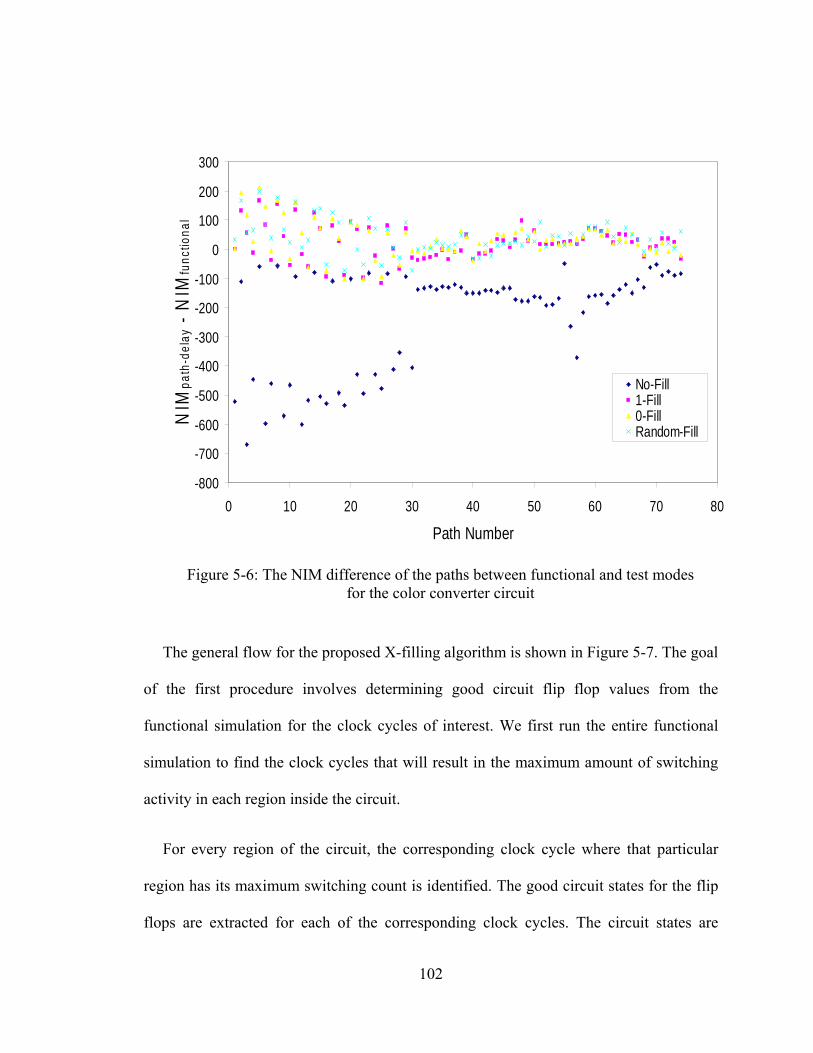
102
-800
-700
-600
-500
-400
-300
-200
-100
0
100
200
300
0 10 20 30 40 50 60 70 80
Path Number
NIM
path
-del
ay -
NIM
func
tiona
l
No-Fill1-Fill0-FillRandom-Fill
Figure 5-6: The NIM difference of the paths between functional and test modes for the color converter circuit
The general flow for the proposed X-filling algorithm is shown in Figure 5-7. The goal
of the first procedure involves determining good circuit flip flop values from the
functional simulation for the clock cycles of interest. We first run the entire functional
simulation to find the clock cycles that will result in the maximum amount of switching
activity in each region inside the circuit.
For every region of the circuit, the corresponding clock cycle where that particular
region has its maximum switching count is identified. The good circuit states for the flip
flops are extracted for each of the corresponding clock cycles. The circuit states are

103
reported with the $monitor built-in Verilog system task. These extracted good circuit
values for the flip flops will be used later in the second procedure of our X-filling
algorithm.
Procedure 1: Functional Don’t Care Bit State Extraction
• Run functional simulation
• Perform regional maximum functional clock cycle analysis
• Extract good circuit states of the flip flops
Procedure 2: Noise Index Model based X’filling
• For every test pattern & for every detected path
• Find the path-to-region relation
• Get the functional clock cycle resulting in maximum switching in the region of interest from Procedure 1
• Get the don’t care bit values in the region of interest from Procedure 1
• Assign the X’s to the extracted circuit states from Procedure 1
Figure 5-7: Proposed NIM-based X-filling Method
In the second procedure, we first determine the path-to-region relation of the circuit.
For every robustly detected path, the location of the path needs to be determined in order

104
to select the appropriate functional clock cycle that we are going to choose. Therefore we
calculated the path-to-region relation based on the x- and y-coordinates of the instances
belonging to the path. Every path instance is checked to find its location with respect to
the regional analysis. If a path is located in two regions (in order words some of the
instances on the path are located in one region and some other instances of the paths are
located in the neighboring region) then the path is assigned to the region that contains the
higher number of path instances.
After the location of the path is determined, we pick the functional clock cycle that
will result in the maximum amount of switching inside the region where the path is. As
we already stated, the path delay test vectors that are generated with the No-Fill option
will result in test vectors with a high number of unspecified bits. In the first procedure,
we determined the good circuit states for the flip flops in the corresponding region for the
clock cycle of interest. Our NIM-X filling algorithm will assign the don’t care bits that are
located in the region of interest to equal the extracted functional states of the flip flops.
Our X-filling algorithm stops when all the flip flops that are physically located inside the
region are assigned to their good circuit states. All the remaining flip flops outside the
region will be left as X’s. However we performed a check to ensure that all of the
standard cells that contribute to the NIM value inside the predefined region are assigned
to a logical value.

105
5.4 Experimental Results
In this section we present experimental results regarding our NIM based X-filling
algorithm. We will show that we can significantly reduce the NIM difference of the paths
between test and functional mode when the don’t care bits are filled with our proposed
algorithm.
-800
-700
-600
-500
-400
-300
-200
-100
0
100
200
0 10 20 30 40 50 60 70 80
Path Number
NIM
path
_del
ay-N
IMfu
nctio
nal
No-FILLNIM-FILL
Figure 5-8: NIM difference between path delay test vectors and functional patterns for No-Fill and NIM-Fill for color converter benchmark
Figure 5-8 shows the NIM difference results for the No-Fill and NIM-Fill options for
the color converter circuit. The test patterns generated with the proposed approach result
in a much lower absolute NIM difference between the test and functional modes. In many

106
cases, the overall switching activity difference is very close to zero. As we have shown in
the previous section, when we fill the don’t care bits with standard filling options we
often get a lot more switching activity around the path, which will lead to overtesting of
the chip.
-12000
-10000
-8000
-6000
-4000
-2000
0
2000
0 50 100 150 200 250 300
Path Number
NIM
path
_del
ay -
NIM
func
tiona
l
NoFillNIM-Fill
Figure 5-9: NIM difference between path delay test vectors and functional patterns for
No-Fill and NIM-Fill for FPU benchmark
One should also realize that for the other X-filling options all the don’t care flip flops
will be assigned to logical values, hence there will be no don’t care bits left in the test
patterns. Static test compaction algorithms which will reduce the test pattern count in a
test set might suffer from this fact and won’t work as efficiently. With the proposed
approach only the flip flops that are in the region of interest will be assigned to logical

107
values; the remaining flip flops far from the location of the critical path will have X’s. As
a result, the static test compaction algorithms can still efficiently work on the test vectors
that are generated with the proposed approach.
The results for the FPU benchmark are shown in Figure 5-9. Again a NIM difference
comparison between test patterns that are generated without any fill option and test
patterns that are generated with the proposed flow is made. As we can see from Figure
5-9 the test patterns generated with the proposed flow are very effective for replicating
the worst case functional switching activity profile around the path of interest.
We have also shown the effectiveness of the NIM-fill approach in Table 5-3. In this
table we show the average of the absolute values of the NIM differences for different fill
options. We can see that the number is significantly reduced when the unspecified bits
are filled with the proposed approach.
Table 5-3 The Average of the Absolute Values of NIM Differences
for Different Fill Options
No-Fill Random-Fill 1-Fill 0-Fill NIM-Fill
Color
Converter
97 46 49 51 27
FPU 98 62 63 71 12

108
5.5 Summary
In this chapter, we first reviewed the previous work on high-quality test pattern
generation. We analyzed the previous work in two categories: pseudo-functional test and
power supply noise aware test pattern generation. We discussed the strengths and
weaknesses of both of the approaches.
Then we have investigated the switching activity profile for both path delay test
vectors and functional operation. We have calculated the noise index values of the critical
paths for path delay test vectors and real functional inputs. We have shown that the noise
index difference of the critical paths between test and functional modes is often large.
Based on the noise index analysis, we observed that certain paths get under-tested
because their noise index value during path delay test mode is much less than their noise
index value during worst case functional mode. On the other hand, we have seen that
some other paths get over-tested because their noise index value during path delay test is
much higher than their noise index value during functional mode.
In order to tackle both of the under-testing and over-testing problems, we have
proposed a noise index model based X-filling algorithm which will extract a subset of the
don’t care bit values from the functional simulation and will assign them to the test
vector accordingly. The test patterns that are generated with the proposed method
replicate the worst case functional switching activity profile around every detected path.
Therefore the likelihood of incorrect test responses (test escapes or yield loss) due to the
power supply switching noise effect on the delay of a path is reduced with the proposed

109
flow. In addition, static test compaction algorithms will still work efficiently on the test
vectors that are generated with the proposed flow because only a subset of the don’t care
bits is assigned.

110
Chapter 6
Conclusions
With the current advances in VLSI technology, the sensitivity of today’s chips to deep
submicron (DSM) effects is increasing. Along with technology scaling, the increase in
the operating frequency and the increase in the functional density of today’s digital
designs has led to new challenges for digital design and test engineers. Managing power
dissipation of the circuit during the functional and test modes has become an arduous
research challenge for the current VLSI design and test engineers. VLSI designers have
exploited various techniques to allow the circuit’s power consumption to remain within
an allowable budget. In this dissertation we focus on the power consumption of the
designs during their test modes, specifically when they are tested with the full scan
methodology.

111
After a brief introduction on power dissipation in digital circuits, in Chapter 2 we
reviewed some of the important concepts necessary for scan-based test and the most
commonly used fault models of manufacturing testing.
Excessive power dissipation of digital circuits during scan-based test is one of the
major problems in digital circuit testing. Many different approaches for reducing the test
power consumption have been proposed in the literature. In Chapter 3, we first reviewed
the DFT- and ATPG-based test power reduction techniques. Both of the techniques try to
reduce the switching activity during test mode. DFT-based approaches modify the circuit
or the scan chain architecture such that the switching activity of the circuit will be
reduced during the scan-based test. In contrast to DFT-based approaches, ATPG-based
approaches alter the test vector generation process such that the switching activity caused
by the generated test set is reduced. Both of these methods have their advantages and
disadvantages. DFT-based modifications usually bring an area or performance overhead
to the design; on the other hand ATPG-based techniques will usually end up with lower
fault coverage or an increase in the test vector size. In this dissertation we introduced a
DFT-based approach which will result in large power reductions during scan shift with
low area and performance overhead.
Later in Chapter 3, we quantitatively analyze the switching activity during the circuit’s
functional and test modes. Our switching activity analysis showed that the switching
activity of the circuit during the shift and capture cycles of the scan-based test is much
more than the switching activity of the circuit during its functional mode. We have
presented a DFT-based technique which reduces the switching activity of the circuit
during the shift-in and shift-out cycles of the scan-based test. Our DFT-based method

112
modifies the circuit by freezing the outputs of a small subset of the flip flops at RT-level
of the design. We take the idea of power-sensitive scan cell identification from [63] and
modify the circuit at a higher level, RTL,. One of the main advantages of this method is
that the modification to the circuit is done at the RTL description of the design as
opposed to modifying the circuit at the gate level. The advantage of this method lies in
the fact that when the extra hardware is inserted at the RTL, the design constraints such
as timing can be handled automatically by the synthesis tool. When the circuit
modification is performed at the gate level, the designers have to re-evaluate the timing
of the circuit. If the additional hardware violates the timing of the design, one can not
insert that extra logic to the circuit. With our proposed method, one can insert the extra
logic to the design without re-evaluating the timing of the circuit.
In Chapter 4, we address another deep submicron DSM related problem—the timing
discrepancies between the design and the silicon. Accurate prediction of the actual path
delays on silicon during the design stage is a hard problem. We have investigated the
amount and characteristics of the timing discrepancies of an industrial design and showed
that the correlation between the predicted delays obtained from SPICE-level timing
analysis and measured delays on silicon is on the order of +/- 75 ps which is well above
measurement inaqualities.. Among all other potential causes for this low correlation, we
have focused on the effects of switching activity on the delay of certain critical paths of
the design. We have presented a noise index mode, NIM, which characterizes the
magnitude of the timing mismatch between silicon and simulation based upon the
switching activity in a well-defined area around the path. We have showed the
effectiveness of the noise index model for predicting delay differences between silicon

113
measurements and pre-silicon estimation with our experiments on the industrial design.
One of the biggest advantages of the proposed noise index model is that the
computational effort to calculate the noise indexes of paths is relatively low. Compared to
past research which requires expensive RC-network analysis and calculation, the noise
index values of the critical paths can be calculated relatively inexpensively.
In Chapter 5, we introduced an ATPG-based technique for generating high quality
path delay test patterns using our noise index model. In contrast with our previously
introduced high level DFT-method, this time we did not only focus on reducing the
switching activity of the circuit. The essential goal of this ATPG-based approach is to
replicate the worst case functional switching activity of the design during the launch
cycle of the path delay test vectors. In Chapter 5, we showed how we have used our
developed noise index model in order to generate a better test set. We have performed a
detailed switching activity analysis and particularly looked at the interaction between the
functional way that the chips are used and the way we test them. The comparison of the
noise index values of the critical paths during test and functional modes has revealed that
significant discrepancies in the noise index values of the critical paths exist between these
two modes of operation. Our noise index analysis indicated that certain paths get under-
tested because their noise index value during path delay test mode is much less than their
noise index value during worst case functional mode. On the other hand, we have seen
that some other paths get over-tested because their noise index value during path delay
test is much higher than their noise index value during functional mode. In order to
generate a high quality test pattern set we tackle both of the over-testing and under-
testing problems at the same time. Our noise index model based test pattern modification

114
technique relies on a don’t care bit filling algorithm which will extract a subset of the
don’t care bit values from the functional simulation and will assign them to the test vector
accordingly. By replicating the worst case functional switching activity profile around the
critical paths, the likelihood of incorrect test responses (test escapes or yield loss) due to
the power supply switching noise effect on the delay of a path is reduced. Previous work
on this area has either relied on vector-less analysis of the circuit to estimate the circuit’s
switching activity during its functional mode or they rely on designer specified threshold
values for the functional mode switching activity calculation. Both of these approaches
are inaccurate in terms of characterizing the circuit’s functional switching activity
behavior. We have simulated the design under characteristic functional inputs including
the timing information of the standard cells and calculated the functional switching
activity of the circuit from this simulation. Then we have used the layout information of
the circuit such that we can relate the functional switching activity of the circuit to the
location of the critical paths. Our proposed method uses a subset of the don’t care bits
and fills them such that the noise index values of the critical paths during the launch
clock cycles will be matched to the worst case functional noise index values of the paths.

115
Bibliography
[1] G. E. Moore, "Cramming More Components Onto Integrated Circuits,"
Electronics, vol. 38, pp. 114 - 117, 1965.
[2] H. P. Hofstee, "Future Microprocessors and Off-Chip SOP Interconnect," IEEE
Transactions on Advances Packaging, vol. 27, pp. 301 - 303, 2004.
[3] International Technology Roadmap for Semiconductors (ITRS)
http://www.public.itrs.net/.
[4] T. Chandra, et al., "A Modeling Approach for Addressing Power Supply
Switching Noise Related Failures of Integrated Circuits," in Design, Automation
and Test in Europe (DATE), 2004, pp. 1078-1083.
[5] M. Pedram and J. M. Rabaey, Power Aware Design Methodologies: Kluwer
Academic Publishers, 2002.
[6] M. L. Bushnell and V. D. Agrawal, Essentials of Electronic Testing for Digital,
Memory & Mixed-Signal VLSI Circuits: Springer, 2000.
[7] P. Girard, "Survey of Low-Power Testing of VLSI Circuits," IEEE Design & Test
of Computers, vol. 19, pp. 80 - 90, 2002.
[8] S. Ravi, "Power-aware test: Challenges and solutions," in International Test
Conference ITC, 2007, pp. 1 - 10.

116
[9] T. Thiel, "Have I Really Met Timing? - Validating PrimeTime Timing Reports
with Spice," in Design Automation and Test in Europe (DATE), 2004, pp. 114 -
119.
[10] P. Pant, et al., "Lessons from At-Speed Scan Deployment on an Intel® Itanium®
Microprocessor," in International Test Conference ITC, 2010.
[11] A. Kokrady and C. P. Ravikumar, "Fast, Layout-Aware Validation of Test-
Vectors for Nanometer-Related Timing Failures," in International Conference on
VLSI Design, 2004, pp. 597 - 602.
[12] M. Williams and J. Angell, "Enhancing Testability of Large-Scale Integrated
Circuits via Test Points and Additional Logic," IEEE Transactions on Computers,
vol. 22, pp. 46 - 60, 1973.
[13] K.-T. Cheng and H.-C. Chen, "Classification and Identification of Nonrobust
Untestable Path Delay Faults," IEEE Transactions on Computer-Aided Design,
vol. 15, pp. 845 - 853, 1996.
[14] N. Devtaprasanna, et al., "Methods for improving transition delay fault coverage
using broadside tests," in IEEE International Test Conference, 2005, pp. 255 -
265.
[15] Y.-T. Lin, et al., "PHS-Fill: A Low Pwer Supply Noise Test Pattern Generation
Technique for At-Speed Scan Testing in Huffman Coding Test Compression
Environment," in Asian Test Symposium ATS, 2008, pp. 391 - 396.
[16] K. M. Butler, et al., "Minimizing Power Consumption in Scan Testing: Pattern
Generation and DFT Techniques," in IEEE International Test Conference ITC,
2004, pp. 355 - 364.

117
[17] X. Wen, et al., "A Novel Scheme to Reduce Power Supply Noise for High-
Quality At-Speed Scan Testing," in International Test Conference (ITC), 2007,
pp. 1-10.
[18] S. Remersaro, et al., "Preferred Fill: A Scalable Method to Reduce Capture Power
for Scan Based Designs," in International Test Conference ITC, 2006, pp. 1 - 10.
[19] A. Chandra and R. Kapur, "Bounded adjacent fill for low capture power scan
testing," in VLSI Test Symposium VTS, 2008, pp. 131 - 138.
[20] C.-W. Tzeng and S.-Y. Huang, "QC-Fill: An X-Fill method for quick-and-cool
scan test," in Design, Automation & Test in Europe DATE, 2009, pp. 1142 - 1147.
[21] N. Badereddine, et al., "Structural-Based Power-Aware Assignment of Don’t
Cares for Peak Power Reduction During Scan Testing," in IFIP International
Conference on Very Large Scale Integration, 2006, pp. 403 - 408.
[22] J. Li, et al., "iFill: An Impact-Oriented X-Filling Method for Shift- and Capture-
Power Reduction in At-Speed Scan-Based Testing," in Design, Automation and
Test in Europe (DATE), 2008, pp. 1184-1189.
[23] K. Enokimoto, et al., "CAt: A Critical- Area-Targeted Test Set Modification
Scheme for Reducing Launch Switching Activity in At- Speed Scan Testing," in
Asian Test Symposium (ATS), 2009, pp. 99-104.
[24] X. Wen, et al., "Critical-Path-Aware X-Filling for Effective IR Drop Reduction in
At Speed Scan Testing," in Design Automation Conference (DAC), 2007, pp. 527-
532.

118
[25] J. Li, et al., "X-Filling for Simultaneous Shift- and Capture-Power Reduction in
At-Speed Scan-based Testing," IEEE Transactions on Verl Large Scale
Integration (VLSI) Systems, pp. 1081 - 1092, 2010.
[26] S. Remersaro, et al., "Low Shift and Capture Power Scan Tests," in International
Conference on VLSI Design, 2007, pp. 793 - 798.
[27] V. Dabholkar, et al., "Techniques for Minimizing Power Dissipation in Scan and
Combinational Circuits During Test Application," IEEE Transactions on
Computer-Aided Design of Integrated Circuits and Systems, vol. 17, pp. 1325 -
1333, 1998.
[28] M. S. Jelodar and K. Mizanian, "Power aware Scan-based testing using genetic
algorithm," in Canadian Conference on Electrical and Computer Engineering
CCECE, 2006.
[29] P. Girard, et al., "Reduction of power consumption during test application by test
vector ordering," Electronics Letters, vol. 33, pp. 1752 - 1754, 1997.
[30] M. Bellos, et al., "Low Power Testing by Test Vector Ordering with Vector
Repetition," in International Symposium on Quality Electronic Design, 2004.
[31] X. Kavousianos, et al., "An efficient test vector ordering method for low power
testing," in IEEE Computer Society Annual Symposium on VLSI ISVLSI, 2004.
[32] S. Roy, et al., "Artificial Intelligence Approach to Test Vector Reordering for
Dynamic Power Reduction During VLSI Testing," in IEEE REgion 10
Conference TENCON, 2008, pp. 1 - 6.

119
[33] H. Hashempour and F. Lombardi, "Evaluation and Analysis of Heuristic
Techniques for Vector Ordering of VLSI Test Sets," IEEE Transactions on
Instrumentation and Measurement, vol. 57, pp. 1998 - 2004, 2008.
[34] T.-C. Huang and K.-J. Lee, "Reduction of Power Consumption in Scan-Based
Circuits during Test Application by an Input Control Technique," IEEE
Transactions on Computer-Aided Design of Integrated Circuits and Systems, vol.
20, pp. 911 - 917, 2001.
[35] J. Wang, et al., "A Vector-based Approach for Power Supply Noise Analysis in
Test Compaction," in International Test Conference (ITC), 2005, pp. 516-526.
[36] Rangonathan Sankaralinga, et al., "Static Compaction Techniques to Control Scan
Vector Power Dissipation," in VLSI Test Symposium VTS, 2000, pp. 35 - 40.
[37] J. Wang, et al., "Static Compaction of Delay Tests Considering Power Supply
Noise," in VLSI Test Symposium VTS, 2005, pp. 235 - 240.
[38] K. Peng, et al., "A Novel Hybrid Method for SDD Pattern Grading and
Selection," in VLSI Test Symposium (VTS), 2010, pp. 45-50.
[39] M. Yilmaz, et al., "Interconnect-Aware and Layout-Oriented Test-Pattern
Selection for Small-Delay Defects," in International Test Conference (ITC), 2008,
pp. 1-10.
[40] H. Lee, et al., "Selecting High-Quality Delay Tests for Manufacturing Test and
Debug," in International Symposium on Defect and Fault Tolerance in VLSI
Systems DFT, 2006, pp. 59 - 70.
[41] M. Yilmaz, et al., "Test-Pattern Grading and Pattern Selection for Small-Delay
Defects," in VLSI Test Symposium VTS, 2008, pp. 233 - 239.

120
[42] Mangoi, et al., "Pattern Selection for Testing of Deep Sub-Micron Timing
Defects," Design Automation and Test in Europe, 2004, pp. 1060 - 1065.
[43] J. Lee and M. Tehranipoor, "LS-TDF: Low-Switching Transition Delay Fault
Pattern Generation," in VLSI Test Symposium (VTS), 2008, pp. 227-232.
[44] J. Lee and M. Tehranipoor, "Layout-Aware Transition-Delay Fault Pattern
Generation with Evenly Distributed Switching Activity," Journal of Low Power
Electronics, vol. 4, pp. 1-12, 2008.
[45] X.Wen, et al., "A new ATPG method for efficient capture power reduction during
scan testing," in VLSI Test Symposium VTS, 2006, pp. 59 - 65.
[46] S. Wang and S. K. Gupta, "ATPG for Heat Dissipation Minimization During Test
Application," IEEE Transactions on Computers, vol. 47, pp. 256 - 262, 1998.
[47] F. Corno, et al., "A Test Pattern Generation Methodology for Low Power
Consumption," in VLSI Test Symposium, 1998, pp. 453 - 457.
[48] V. R. Devanathan, et al., "Glitch-Aware Pattern Generation and Optimization
Framework for Power-Safe Scan Test," in VLSI Test Symposium VTS, 2007, pp.
167 - 172.
[49] J. Zhang, et al., "Multi-phase Clock Scan Technique for Low Test Power," in
International Symposium on High Density Packaging and Microsystem
Integration, 2007, pp. 1 - 5.
[50] T.-C. Huang and K.-J. Lee, "A Token Scan Architecture for Low Power Testing,"
in International Test Conference, 2001, pp. 660 - 669.
[51] G. Dai, et al., "DCScan: A Power-Aware Scan Testing Architecture," in Asian
Test Symposium, 2008, pp. 343 - 348.

121
[52] M.-H. Chiu and J. C.-M. Li, "Jump scan: A DFT Technique for Low Power
Testing," in VLSI Test Symposium VTS, 2005, pp. 277 - 282.
[53] P. Rosinger, et al., "Scan Architecture With Mutually Exclusive Scan Segment
Activation for Shift- and Capture-Power Reduction," IEEE Transactions on
Computer-Aided Design of Integrated Circuits and Systems, vol. 23, pp. 1142 -
1153, 2004.
[54] Y. Bonhomme, et al., "A Gated Clock Scheme for Low Power Scan Testing of
Logic IC’s or embedded cores," in Asian Test Symposium, 2001, pp. 253 - 258.
[55] N. Nicolici and B. M. Al-Hashimi, "Multiple scan chains for power minimization
during test application in sequential circuits," IEEE Transactions on Computers,
vol. 51, pp. 721 - 734, 2002.
[56] L. Whetsel, "Adapting Scan Architectures for Low Power Operation," in
International Test Conference ITC, 2000, pp. 863 - 872.
[57] S. Gerstendorfer and H.-J. Wunderlich, "Minimized Power Consumption for
Scan-Based BIST," in International Test Conference ITC, 1999, pp. 77 - 84.
[58] S. Bhunia, et al., "Low-Power Scan Design using First-Level Supply Gating,"
IEEE Transactions on Very Large Scale Integration (VLSI) Systems, vol. 13, pp.
384 - 395, 2005.
[59] R. Datta, et al., "Testing and Debugging Delay Faults in Dynamic Circuits," in
International Test Conference ITC, 2005, pp. 100 - 110.
[60] R. Sankaralingam and N. A. Touba, "Inserting Test Points to Control Peak Power
During Scan Testing," in IEEE International Symposium on Defect and Fault
Tolerance in VLSI Systems, 2002, pp. 138 - 146.

122
[61] M. ElShoukry, et al., "Partial Gating Optimization for Power Reduction During
Test Application," in Asian Test Symposium ATS, 2005, pp. 242 - 247.
[62] O. Sinanoglu, et al., "Test Power Reduction through Minimization of Scan Chain
Transitions," in VLSI Test Symposium VTS, 2002, pp. 166 - 171.
[63] X. Lin and Y. Huang, "Scan Shift Power Reduction by Freezing Power Sensitive
Scan Cells," Journal of Electronic Testing: Theory and Applications JETTA, vol.
24, pp. 327 - 334, 2008.
[64] www.opencores.org.
[65] V. D. Agrawal and S. Seth, "Mutually Disjoint Signals and Probability
Calculation in Digital Circuits," in Great Lakes Symposium on VLSI GLSVLSI,
1998, pp. 307 - 312.
[66] A. Ghosh, et al., "Estimation of Average Switching Activity in Combinational
and Sequential Circuits," in Design Automation Conference DAC, 1992, pp. 253 -
259.
[67] D. Josephson, "The Good, the Bad, and the Ugly of Silicon Debug," in
ACM/IEEE Design Automation Conference DAC, 2006, pp. 3 - 6.
[68] J. Keshava, et al., "Post-silicon Validation Challenges: How EDA and Academia
Can Help," in ACM/IEEE Design Automation Conference DAC, 2010, pp. 3 - 7.
[69] P. Bastani, et al., "Speedpath Prediction Based on Learning from a Small Set of
Example," in Design Automation Conference DAC, 2008, pp. 2187-222.
[70] P. Bastani, et al., "Linking Statistical Learning to Diagnosis," IEEE Design &
Test of Computers, vol. 25, pp. 232 - 239.

123
[71] P. Bastani, et al., "Diagnosis of design-silicon timing mismatch with feature
encoding and importance ranking – the methodology explained," in International
Test Conference ITC, 2008, pp. 1 - 10.
[72] N. Callegari, et al., "Path Selection for monitoring unexpected systematic timing
effects," in Asia and South Pasific Design Automation Confrence, 2009, pp. 781 -
786.
[73] L. Xie and A. Davoodi, "Representative Path Selection for Post-Silicon Timing
Prediction Under Variability," in ACM/IEEE Design Automation Conference
DAC, 2010, pp. 386 - 391.
[74] J. Chen, et al., "Mining AC Delay Measurements for Understanding Speed-
limiting Paths," in International Test Conference, 2010.
[75] Q. Liu and S. S. Sapatnekar, "Synthesizing a representative critatical path for
post-silicon delay prediction," in International Symposium on Physical Design
ISPD, 2009.
[76] G. Bai, et al., "Maximum Power Supply Noise Estimation in VLSI Circuts Using
Multimodal Genetic Algorithms," in International Conference on Electronics,
Circuits and Systems (ICECS), 2001, pp. 1437-1440.
[77] S. Zhao, et al., "Estimation of Inductive and Resistive Switching Noise on Power
Supply Network in Deep Sub-micron CMOS Circuits," in International
Conference on Computer Design (ICCD), 2000, pp. 65-72.
[78] S. Zhao and K. Roy, "Estimation of Switching Noise on Power Supply Lines in
Deep Sub-micron CMOS Circuits," in International Conference on VLSI Design,
2000, pp. 168-173.
124
[79] Y.-M. Jiang, et al., "Estimation of Maximum Power Supply Noise for Deep Sub-
Micron Designs," Low Power Electronics and Design, pp. 233-238, 1998.
[80] J. Wang, et al., "Modeling Power Supply Noise in Delay Testing," IEEE Design
& Test of Computers, vol. 24, pp. 226-234, 2007.
[81] G. Bai, et al., "Maximum power supply noise estimation in VLSI circuits using
multimodal genetic algorithms," in IEEE International Conference on
Electronics, Circuits and Systems ICECS, 2001, pp. 1437 - 1440.
[82] Y.-M. Jiang, et al., "Estimation of Maximum Power and Instantaneous Current
Using a Genetic Algorithm," in Custom Integrated Circuits Conference, 1997, pp.
135-138.
[83] S. Devadas, et al., "Estimation of Power Dissipation in CMOS Combinational
Circuits Using Boolean Function Manipulation," IEEE Transactions on
Computer-Aided Design of Integrated Circuits and Systems, vol. 11, pp. 373 -
383, 1992.
[84] C.-Y. Wang and K. Roy, "Maximum Power Estimation for CMOS Circuits Using
Deterministic and Statistic Approaches," in International Conference on VLSI
Design, 1996, pp. 364 - 369.
[85] A. Krstic and K.-T. Cheng, "Vector Generation for Maximum Instantaneous
Current Through Supply Lines for CMOS Circuits," in Design Automation
Conference DAC, 1997, pp. 383 - 388.
[86] H. Kriplani, et al., "Pattern Independent Maximum Current Estimation in Power
and Ground Buses of CMOS VLSI Circuits: Algorithms, Signal Correlations, and

125
Their Resolution," IEEE Transactions on Computer-Aided Design of Integrated
Circuits and Systems, vol. 14, pp. 998 - 1012, 1995.
[87] W. M. Heuvelman, "Theory of Decap Location in an SoC," 2008.
[88] M. Popovich, et al., "Effective Radii of On-Chip Decoupling Capacitors," IEEE
Transactions on Very Large Scale Integration (VLSI) Systems, vol. 16, 2008.
[89] H. H. Chen and S. E. Schuster, "On-Chip Decoupling Capacitor Optimization for
High-Performance VLSI Design," in International Symposium on VLSI
Technology, Systems and Applications, 1995, pp. 99 - 103.
[90] H. Su, et al., "Optimal decoupling capacitor sizing and placement for standard-
cell layout designs," IEEE Transactions on Computer-Aided Design of Integrated
Circuits and Systems, vol. 22, pp. 428 - 436, 2003.
[91] M. Popovich, et al., "Maximum effective distance of on-chip decoupling
capacitors in power distribution grids," in ACM/IEEE Great Lakes Symp. VLSI,
2006, pp. 173 - 179.
[92] Q. K. Zhu, et al., "Decoupling Capacitance Study and Optimization Method for
High-Performance VLSIs," in IEEE International Symposium on Design and
Diagnostic of Electronic Circuits and Systems, 2010, pp. 388 - 392.
[93] M. Popovich, et al., "Efficient Placement of Distributed On-Cip Decoupling
Capacitors in Nanoscale ICs," in IEEE/ACM International Conference on
Computer-Aided Design, 2007, pp. 811 - 816.
[94] Y.-C. Lin, et al., "Pseudofunctional Testing," Transactions on Computer-Aided
Design of Integrated Circuits and Systems, pp. 1535-1546, 2006.

126
[95] Z. Zhang, et al., "On Generating Pseudo-Functional Delay Fault Tests for Scan
Designs," in Defect and Fault Tolerance in VLSI Systems, 2005, pp. 398-405.
[96] F. Yuan and Q. Xu, "On Systematic Illegal State Identification for Pseudo-
Functional Testing," in Design and Automation Conference (DAC), 2009, pp.
702-707.
[97] I. Pomeranz and S. M. Reddy, "Forming Multi-Cycle Tests for Delay Faults by
Concatenating Broadside Tests," in VLSI Test Symposium (VTS), 2008, pp. 51-56.
[98] E. Moghaddam, et al., "Low Capture Power At-Speed Test in EDT Environment,"
in International Test Conference ITC, 2010.
[99] F. Yuan and Q. Xu, "Compression-Aware Pseudo-Functional Testing," in
International Test Conference (ITC), 2009, pp. 1-10.
[100] X. Liu, et al., "Layout-Aware Pseudo-Functional Testing for Critical Paths
Considering Power Supply Noise Effects," in Design, Automation and Test
Conference in Europe (DATE), 2010, pp. 1432-1437.
[101] W. Jing, et al., "A vector-based approach for power supply noise analysis in test
compaction," in International Test Conference (ITC), 2005, pp. 516-526.
[102] http://www.jhauser.us/arithmetic/SoftFloat.html.