Absorptive Reflectionless Filters
81
Portland State University Portland State University PDXScholar PDXScholar Dissertations and Theses Dissertations and Theses 3-11-2020 Absorptive Reflectionless Filters Absorptive Reflectionless Filters Guy Barry Lemire Portland State University Follow this and additional works at: https://pdxscholar.library.pdx.edu/open_access_etds Part of the Electrical and Computer Engineering Commons Let us know how access to this document benefits you. Recommended Citation Recommended Citation Lemire, Guy Barry, "Absorptive Reflectionless Filters" (2020). Dissertations and Theses. Paper 5501. https://doi.org/10.15760/etd.7375 This Thesis is brought to you for free and open access. It has been accepted for inclusion in Dissertations and Theses by an authorized administrator of PDXScholar. Please contact us if we can make this document more accessible: [email protected].
Transcript of Absorptive Reflectionless Filters
Portland State University Portland State University
PDXScholar PDXScholar
Dissertations and Theses Dissertations and Theses
3-11-2020
Absorptive Reflectionless Filters Absorptive Reflectionless Filters
Guy Barry Lemire Portland State University
Follow this and additional works at: https://pdxscholar.library.pdx.edu/open_access_etds
Part of the Electrical and Computer Engineering Commons
Let us know how access to this document benefits you.
Recommended Citation Recommended Citation Lemire, Guy Barry, "Absorptive Reflectionless Filters" (2020). Dissertations and Theses. Paper 5501. https://doi.org/10.15760/etd.7375
This Thesis is brought to you for free and open access. It has been accepted for inclusion in Dissertations and Theses by an authorized administrator of PDXScholar. Please contact us if we can make this document more accessible: [email protected].
Absorptive Reflectionless Filters
by
Guy Barry Lemire
A thesis submitted in partial fulfillment of the requirements for the degree of
Master of Science in
Electrical and Computer Engineering
Thesis Committee: Branimir Pejcinovic, Chair
Martin Siderius Richard Campbell
Portland State University 2020
i
Abstract
For many applications requiring some sort of signal filtering or signal
conditioning, the filter requirements are usually approached with a single purpose in
mind, which is to maximize both passband signal amplitude and stop band signal
attenuation to the load with little to no thought given to what happens to the stop band
signal energy. Many conventional filters have very poor impedance matching in the
stopband resulting in reflected energy or large return loss (S11). This reflected energy
can then cause interactions with adjoining system components which do not in general
respond well to spurious reflected energy and can result in degradation of system
performance or other unintended consequences [1].
This thesis implements and verifies the design procedure and examines the
frequency scaling of a novel passive filter design methodology proposed by Morgan and
Boyd [2] which the authors claim results in an easy to realize reflectionless filter which
has stopband reflection response superior to conventional passive filters. Following the
proposed design methodology, a reflectionless filter was simulated and then realized in
a hardware prototype and good agreement observed between simulation and
measurement results. To determine the quality of stopband response, the reflectionless
filter response was compared to a Butterworth admittance complimentary diplexer
designed using accepted techniques [3], [4], [5]. The reflectionless filter showed similar
measured stopband response to the diplexer but this was gained with a much simpler
design process than was required for the diplexer.

ii
To verify the ability of the procedure to scale the design requirements, a filter
with a decade wider bandwidth was also designed and the measured response
compared to a similarly scaled Butterworth diplexer. For this frequency range of
interest, the reflectionless filter exhibited superior stopband rejection when compared
to the diplexer. Simulation and measured results were in good agreement for both
filters.
In conclusion, this work was able to realize a reflectionless filter using Morgan
and Boyd’s design procedure and the measured results were in good agreement with
simulation results. The stopband of the reflectionless filter was comparable to a similar
diplexer but with much less design effort required. The scaling of design parameters for
reflectionless filters was also demonstrated.

iii
Dedication
To Nancy De Martino

iv
Acknowledgements
I would like to thank the following people and institutions who were instrumental in
their support during the progress of this work. I would like to thank my advisor Branimir
Pejcinovic for his help and guidance in making this a great learning experience. My
committee members, Richard Campbell and Martin Siderius for their time and insightful
suggestions. I wanted to thank Matthew A. Morgan for his very generous help in
promptly and fully answering my questions. I would like to thank Synopsys for the use of
their lab facilities and equipment and my manager Christian de Verteuil for his patience
in allowing me to spend time to focus on completing this work. I would like to thank
both Modelithics and Keysight for the support and student licenses for their respective
software which allowed me to complete this work.

v
Table of Contents
Abstract............................................................................................................................................ i
Dedication ..................................................................................................................................... iii
Acknowledgements ...................................................................................................................... iv
List of Tables ................................................................................................................................. vii
List of Figures ............................................................................................................................... viii
Glossary ..........................................................................................................................................ix
Chapter 1: Introduction ................................................................................................................ 1
Chapter 2: Background and Theory ............................................................................................ 5
2.1 Even-Odd Mode Analysis ............................................................................................ 10 2.2 Filter Design Procedure ............................................................................................... 13 2.2.1 Step 1 – Even Mode Equivalent Half Circuit ............................................................ 13 2.2.2 Step 2 – Odd Mode Equivalent Half Circuits ............................................................ 14 2.2.3 Step 3 – Symmetrical Topology ............................................................................... 15 2.2.4 Step 4 - Determination of Component Values......................................................... 18 2.3 Single Stage Nth order Filters ..................................................................................... 19 Chapter 3: Reflectionless Filter Realization - Simulation ....................................................... 22
3.1 Design of Ideal Filter ................................................................................................... 22 3.2 Simulation of Ideal Low-Pass Filter ............................................................................. 26 3.3 Ideal Low-Pass Filter Results ....................................................................................... 27 3.4 Simulation of Non-ideal Filter ..................................................................................... 29 3.4.1 Non-ideal Components ............................................................................................ 29 3.4.2 PCB Stack-up ............................................................................................................ 30 3.4.3 Microstrip Transmission Lines ................................................................................. 30 3.4.4 ADS Non-ideal Testbench ........................................................................................ 31 3.5 Comparing Ideal and Non-Ideal Simulated Filter Results ........................................... 33 Chapter 4: Filter Realization – Fabrication .............................................................................. 35
4.1 PCB Schematic Design ................................................................................................. 35 4.2 PCB Layout and Assembly ........................................................................................... 38 4.3 Butterworth Diplexer .................................................................................................. 40 Chapter 5: Experimental Results ............................................................................................... 41
5.1 Frequency Scaling ....................................................................................................... 48 Chapter 6: Discussion, Conclusions and Future Work ........................................................... 51
6.1 Discussion .................................................................................................................... 51 6.2 Conclusion ................................................................................................................... 54 6.3 Future Work ................................................................................................................ 54 References .................................................................................................................................... 57
Appendix A - Butterworth Diplexer .......................................................................................... 59
Appendix B - VNA Calibration .................................................................................................... 63
Appendix C - Automatic Fixture Removal (AFR) ...................................................................... 64
Appendix D – Simulation Library ............................................................................................... 66
Appendix E – Duality ................................................................................................................... 68

vi
Appendix F – Inverse Chebyshev ............................................................................................... 69

vii
List of Tables
Table 1: Anti-aliasing filter design requirements .............................................................. 22
Table 2: Ideal reflectionless element values per stage ..................................................... 24 Table 3: Reflectionless 188MHz component values ......................................................... 31
viii
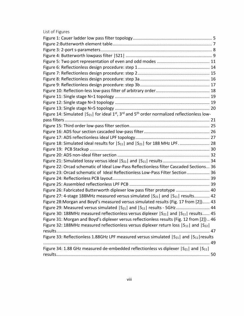
List of Figures
Figure 1: Cauer ladder low pass filter topology .................................................................. 5 Figure 2:Butterworth element table ................................................................................... 7 Figure 3: 2-port s-parameters ............................................................................................. 8 Figure 4: Butterworth lowpass filter |S21| ........................................................................ 9 Figure 5: Two port representation of even and odd modes ............................................ 11 Figure 6: Reflectionless design procedure: step 1 ............................................................ 14 Figure 7: Reflectionless design procedure: step 2 ............................................................ 15 Figure 8: Reflectionless design procedure: step 3a .......................................................... 16 Figure 9: Reflectionless design procedure: step 3b .......................................................... 17 Figure 10: Reflection-less low-pass filter of arbitrary order ............................................. 18 Figure 11: Single stage N=1 topology ............................................................................... 19 Figure 12: Single stage N=3 topology ............................................................................... 19 Figure 13: Single stage N=5 topology ............................................................................... 20 Figure 14: Simulated |S21| for ideal 1st, 3rd and 5th order normalized reflectionless low-pass filters ......................................................................................................................... 21 Figure 15: Third order low-pass filter section ................................................................... 25 Figure 16: ADS four section cascaded low-pass filter ....................................................... 26 Figure 17: ADS reflectionless ideal LPF topology .............................................................. 27 Figure 18: Simulated ideal results for |S11| and |S21| for 188 MHz LPF. ......................... 28 Figure 19: PCB Stackup .................................................................................................... 30 Figure 20: ADS non-ideal filter section ............................................................................. 32 Figure 21: Simulated lossy versus ideal |S21| and |S11| results ....................................... 34 Figure 22: Orcad schematic of Ideal Low-Pass Reflectionless filter Cascaded Sections ... 36 Figure 23: Orcad schematic of Ideal Reflectionless Low-Pass Filter Section ................... 36 Figure 24: Reflectionless PCB layout ................................................................................. 39 Figure 25: Assembled reflectionless LPF PCB ................................................................... 39 Figure 26: Fabricated Butterworth diplexer low pass filter prototype ............................ 40 Figure 27: 4-stage 188MHz measured versus simulated |S21| and |S11| results............. 42 Figure 28:Morgan and Boyd’s measured versus simulated results (Fig. 17 from [2])...... 43 Figure 29: Measured versus simulated |S21| and |S11| results - 5GHz ............................ 44 Figure 30: 188MHz measured reflectionless versus diplexer |S21| and |S11| results ...... 45 Figure 31: Morgan and Boyd’s diplexer versus reflectionless results (Fig. 12 from [2]) .. 46 Figure 32: 188MHz measured reflectionless versus diplexer return loss |S11| and |S22| results ................................................................................................................................ 47 Figure 33: Reflectionless 1.88GHz LPF measured versus simulated |S21| and |S11|results........................................................................................................................................... 49 Figure 34: 1.88 GHz measured de-embedded reflectionless vs diplexer |S21| and |S11| results ................................................................................................................................ 50
ix
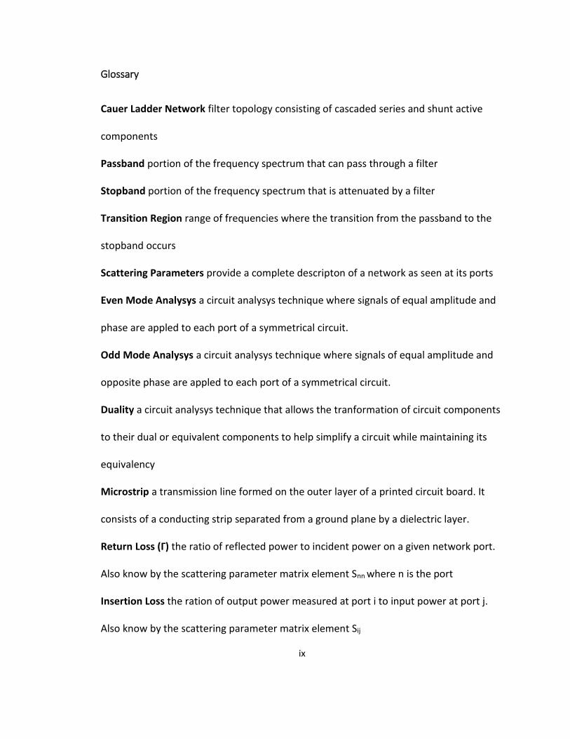
Glossary
Cauer Ladder Network filter topology consisting of cascaded series and shunt active
components
Passband portion of the frequency spectrum that can pass through a filter
Stopband portion of the frequency spectrum that is attenuated by a filter
Transition Region range of frequencies where the transition from the passband to the
stopband occurs
Scattering Parameters provide a complete descripton of a network as seen at its ports
Even Mode Analysys a circuit analysys technique where signals of equal amplitude and
phase are appled to each port of a symmetrical circuit.
Odd Mode Analysys a circuit analysys technique where signals of equal amplitude and
opposite phase are appled to each port of a symmetrical circuit.
Duality a circuit analysys technique that allows the tranformation of circuit components
to their dual or equivalent components to help simplify a circuit while maintaining its
equivalency
Microstrip a transmission line formed on the outer layer of a printed circuit board. It
consists of a conducting strip separated from a ground plane by a dielectric layer.
Return Loss (Γ) the ratio of reflected power to incident power on a given network port.
Also know by the scattering parameter matrix element Snn where n is the port
Insertion Loss the ration of output power measured at port i to input power at port j.
Also know by the scattering parameter matrix element Sij

x
De-embedding the mathematical act of removing the effects of a test fixture so that the
device response can be directly measured.

1
Chapter 1: Introduction
Maximizing useful signal power from the source to the load has been a fundamental
design goal in electrical networks since the dawn of modern electronics in the early 20th
century [6], [7]. The mechanism for this matching source to load impedance was usually
through some intermediary circuit located between the source and the load. The
impedance matching network or more generally “filter” can be as simple as a single
termination resistor placed near the load, to an active multitap adaptive broadband
filter to quarter wavelength microstrip stubs. Regardless of complexity or target
application in which the filter is required, these structures can have one or several
design parameters to be optimized which are (but not limited to)
• maximum power transfer
• selective filtering (passband) for a frequency range of interest and
• controlling reflection of the signal from the load in an unwanted (stopband) frequency range of interest
• waveform shaping maximizing signal to noise ratio Depending on the application and filter topology chosen, in general the design becomes
more difficult and complex the more design parameters that need to be optimized.
Additionally, many of the current solutions have problems or shortcomings which
include inherently limited bandwidth (e.g. quarter wavelength stubs), excessive
passband loss, reflective peaking in the transition region and can have a large physical
topology which makes implementation difficult for space limited applications. Often the
shortcomings of the filter design necessitate additional elements that need to be
inserted into the system design to mitigate the unwanted effects.
2
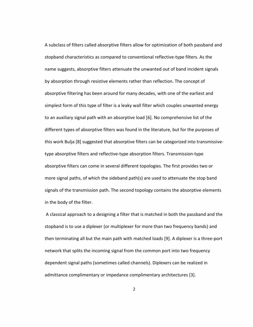
A subclass of filters called absorptive filters allow for optimization of both passband and
stopband characteristics as compared to conventional reflective-type filters. As the
name suggests, absorptive filters attenuate the unwanted out of band incident signals
by absorption through resistive elements rather than reflection. The concept of
absorptive filtering has been around for many decades, with one of the earliest and
simplest form of this type of filter is a leaky wall filter which couples unwanted energy
to an auxiliary signal path with an absorptive load [6]. No comprehensive list of the
different types of absorptive filters was found in the literature, but for the purposes of
this work Bulja [8] suggested that absorptive filters can be categorized into transmissive-
type absorptive filters and reflective-type absorption filters. Transmission-type
absorptive filters can come in several different topologies. The first provides two or
more signal paths, of which the sideband path(s) are used to attenuate the stop band
signals of the transmission path. The second topology contains the absorptive elements
in the body of the filter.
A classical approach to a designing a filter that is matched in both the passband and the
stopband is to use a diplexer (or multiplexer for more than two frequency bands) and
then terminating all but the main path with matched loads [9]. A diplexer is a three-port
network that splits the incoming signal from the common port into two frequency
dependent signal paths (sometimes called channels). Diplexers can be realized in
admittance complimentary or impedance complimentary architectures [3].

3
To address the out of band reflective problem a novel methodology for absorptive filters
has been recently proposed by Morgan and Boyd [2]. Morgan terms these filters
reflectionless rather than absorptive because theoretically they have reflection
coefficients of zero at all ports for all frequencies for ideal elements [10]. To follow
Morgan’s terminology, these filters will be designated henceforth as reflectionless. This
filter has the similar out of band properties as a diplexer but with a simpler design
process and more importantly, all ports are matched due to symmetry. This allows for
cascading of reflectionless filter sections without the debilitating inter-stage interaction
found with many filters.
This thesis will demonstrate the process of design, simulation and realization of a
reflectionless filter based on the design criteria outlined in Morgan and Boyd. The
realized prototype filter will be measured with a Vector Network Analyzer (VNA), and
the results compared to the Morgan paper results in a Scattering Parameter (S-
parameter) format. Additionally, a Butterworth diplexer will be designed, a prototype
measured, and the results will be compared to the reflectionless filter. To further
illustrate the design properties, a filter will be scaled by a decade above the Morgan and
Boyd paper and the results measured and presented.
A description of the theoretical background and assumptions that are made in the
reflectionless design methodology will be demonstrated in Chapter 2. Specifically, it will
be discussed how Morgan and Boyd use even and odd mode analysis, duality and
symmetry to obtain important mathematical relationships that will guide the topology

4
of the normalized filters. The optimum filter order is determined as well as component
values. In Chapter 3 simulations are performed for a reflectionless filter with ideal
design parameters and a reflectionless filter with non-ideal elements and microstrip
transmission lines. Both results are compared to Morgan’s results to check on the
validity of the design process in this work. Chapter 4 outlines the PCB layout decisions
and fabrication materials. Chapter 5 presents the laboratory results for both the
reflectionless filter and the diplexer and compares them to the Morgan results. Chapter
6 is a discussion of the results followed by conclusions and some ideas for future work.
5
Chapter 2: Background and Theory
Filter design methodologies has evolved to where a generally accepted or canonical
approach can be used to realize a design. The designer need not have intimate
knowledge of the underlying mathematical concepts but simply follow a set of steps to
realize a filter which meets the design requirements. Filter responses can mostly be
categorized by the frequencies that the filters pass or allow through, such as low pass,
band pass or high pass. Several types of filters families such as the Butterworth,
Chebyshev, Elliptical and Bessel can be designed to meet the frequency responses
desired but each family will have slightly different response signatures.
A basic overview of the canonical approach to filter design will be presented in this
chapter and without loss of generality will involve the design of a low pass Butterworth
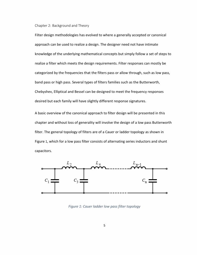
filter. The general topology of filters are of a Cauer or ladder topology as shown in
Figure 1, which for a low pass filter consists of alternating series inductors and shunt
capacitors.
Figure 1: Cauer ladder low pass filter topology

6
As can be seen from the Cauer topology, the ladder network consists of a total of n
elements where n represents the order of the filter. When designing a low pass filter the
first step is to determine the number of component required to meet the design
requirement. Usually a filter design has both a 3dB bandwidth (ωc) and a desired
stopband attenuation at a specified frequency (ωs), and from these two parameters it is
possible to determine the number of components or the order of the filter n.
Once the order of the filter has been determined, the next step requires a simple table
lookup of the normalized component values as shown in Figure 2, [11] and can be
directly read from the row corresponding to the filter order n.
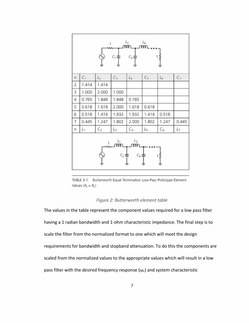
7
Figure 2: Butterworth element table
The values in the table represent the component values required for a low pass filter
having a 1 radian bandwidth and 1-ohm characteristic impedance. The final step is to
scale the filter from the normalized format to one which will meet the design
requirements for bandwidth and stopband attenuation. To do this the components are
scaled from the normalized values to the appropriate values which will result in a low
pass filter with the desired frequency response (ωc) and system characteristic
8
impedance (Zo). Equations (1), (2) show the relationship between the scaled component
values L’n, C’
n and the normalized component values Ln, Cn.
𝐿𝑛′ =
Ln∗Zo
𝜔𝑐 (1)
𝐶𝑛′ =
Cn∗Yo
𝜔𝑐 (2)
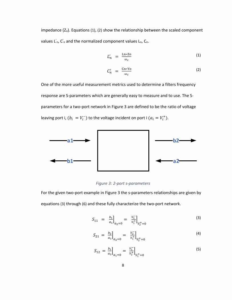
One of the more useful measurement metrics used to determine a filters frequency
response are S-parameters which are generally easy to measure and to use. The S-
parameters for a two-port network in Figure 3 are defined to be the ratio of voltage
leaving port i, (𝑏𝑖 = 𝑉𝑖−) to the voltage incident on port i (𝑎𝑖 = 𝑉𝑖
+).
b2a1
b1 a2
Figure 3: 2-port s-parameters
For the given two-port example in Figure 3 the s-parameters relationships are given by
equations (3) through (6) and these fully characterize the two-port network.
𝑆11 = 𝑏1
𝑎1]
𝑎2=0=
𝑉1−
𝑉1+]
𝑉2+=0
(3)
𝑆21 = 𝑏2
𝑎1]
𝑎2=0=
𝑉2−
𝑉1+]
𝑉2+=0
(4)
𝑆12 = 𝑏1
𝑎2]
𝑎1=0=
𝑉1−
𝑉2+]
𝑉1+=0
(5)
9
𝑆22 = 𝑏2
𝑎2]
𝑎1=0=
𝑉2−
𝑉2+]
𝑉1+=0
(6)
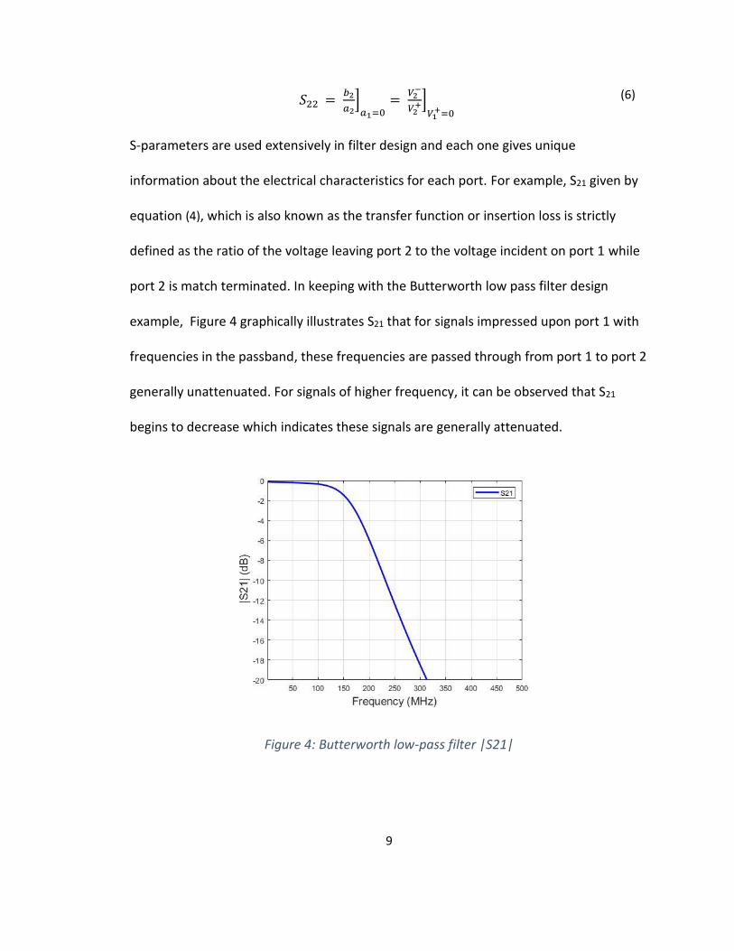
S-parameters are used extensively in filter design and each one gives unique
information about the electrical characteristics for each port. For example, S21 given by
equation (4), which is also known as the transfer function or insertion loss is strictly
defined as the ratio of the voltage leaving port 2 to the voltage incident on port 1 while
port 2 is match terminated. In keeping with the Butterworth low pass filter design
example, Figure 4 graphically illustrates S21 that for signals impressed upon port 1 with
frequencies in the passband, these frequencies are passed through from port 1 to port 2
generally unattenuated. For signals of higher frequency, it can be observed that S21
begins to decrease which indicates these signals are generally attenuated.
Figure 4: Butterworth low-pass filter |S21|

10
For this work s-parameters will be used extensively to describe both simulated and
measured results. They will also be used to compare and to evaluate the quality of filter
results.
The procedure to realize reflectionless filters is by no means canonical. The theory and
procedure for a reflectionless filter comes directly from Morgan and Boyd’s paper in
which the authors outline the steps required to design and realize this type of filter. The
proposed methodology makes use of even-odd mode analysis, symmetry, duality and
couples these basic concepts with Cauer ladder network topologies for filters to realize a
unique topology for reflection-less filters. Symmetry follows from even-odd mode
analysis and this allows the derived filter to have impedance matching at all ports, which
implies that the cascading of these structures is at least theoretically possible without
interactions between stages.
2.1 Even-Odd Mode Analysis
Even-odd mode analysis is based on Bartlett’s bisection theorem [12] and uses
symmetry and superposition to help analyze symmetrical circuits. The general idea is
that for a symmetrical two-port network two independent types of port excitation
(defined as even-mode and odd-mode) when applied to the circuit, certain circuit
behaviors can be realized. Even-mode excitation is defined as impressing two signals
which are equal in both magnitude and phase on each port simultaneously. Odd-mode
excitation is defined as impressing two signals equal in magnitude but opposite in phase
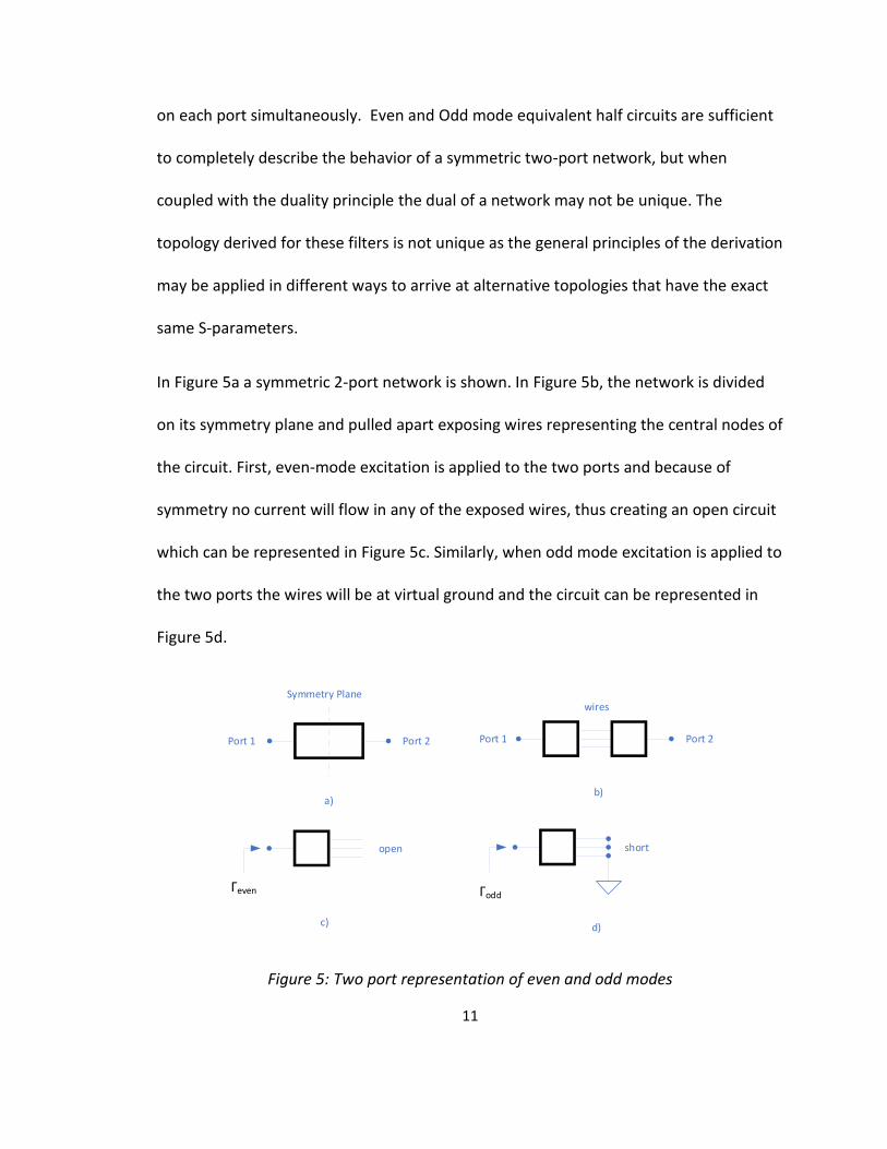
11
on each port simultaneously. Even and Odd mode equivalent half circuits are sufficient
to completely describe the behavior of a symmetric two-port network, but when
coupled with the duality principle the dual of a network may not be unique. The
topology derived for these filters is not unique as the general principles of the derivation
may be applied in different ways to arrive at alternative topologies that have the exact
same S-parameters.
In Figure 5a a symmetric 2-port network is shown. In Figure 5b, the network is divided
on its symmetry plane and pulled apart exposing wires representing the central nodes of
the circuit. First, even-mode excitation is applied to the two ports and because of
symmetry no current will flow in any of the exposed wires, thus creating an open circuit
which can be represented in Figure 5c. Similarly, when odd mode excitation is applied to
the two ports the wires will be at virtual ground and the circuit can be represented in
Figure 5d.
Symmetry Plane
Port 1 Port 2 Port 1 Port 2
open
wires
short
a)b)
c) d)
Γeven Γodd
Figure 5: Two port representation of even and odd modes
12
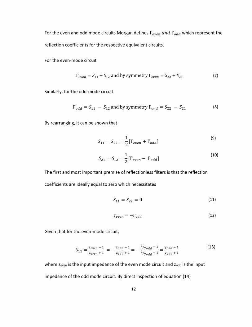
For the even and odd mode circuits Morgan defines Г𝑒𝑣𝑒𝑛 𝑎𝑛𝑑 Г𝑜𝑑𝑑 which represent the
reflection coefficients for the respective equivalent circuits.
For the even-mode circuit
Г𝑒𝑣𝑒𝑛 = 𝑆11 + 𝑆12 and by symmetry Г𝑒𝑣𝑒𝑛 = 𝑆22 + 𝑆21 (7)
Similarly, for the odd-mode circuit
Г𝑜𝑑𝑑 = 𝑆11 − 𝑆12 and by symmetry Г𝑜𝑑𝑑 = 𝑆22 − 𝑆21 (8)
By rearranging, it can be shown that
𝑆11 = 𝑆22 =
1
2[Г𝑒𝑣𝑒𝑛 + Г𝑜𝑑𝑑]
(9)
𝑆21 = 𝑆12 =
1
2[Г𝑒𝑣𝑒𝑛 − Г𝑜𝑑𝑑]
(10)
The first and most important premise of reflectionless filters is that the reflection
coefficients are ideally equal to zero which necessitates
𝑆11 = 𝑆22 = 0 (11)
Г𝑒𝑣𝑒𝑛 = −Г𝑜𝑑𝑑
(12)
Given that for the even-mode circuit,
𝑆11 =
z𝑒𝑣𝑒𝑛 − 1
z𝑒𝑣𝑒𝑛 + 1 = −
z𝑜𝑑𝑑 − 1
z𝑜𝑑𝑑 + 1= −
1y𝑜𝑑𝑑
⁄ − 1
1y𝑜𝑑𝑑
⁄ + 1=
y𝑜𝑑𝑑 − 1
y𝑜𝑑𝑑 + 1
(13)
where zeven is the input impedance of the even mode circuit and zodd is the input
impedance of the odd mode circuit. By direct inspection of equation (14)
13
z𝑒𝑣𝑒𝑛 = 𝑦𝑜𝑑𝑑 (14)
Equation (14) is the duality condition between even and odd mode circuits and will be
important when realizing reflection-less filters. Another equally important result is
obtained by substituting (12) into (10) giving
𝑆21 = Г𝑒𝑣𝑒𝑛 (15)
Examining equation (15) closely indicates that frequencies that are reflective in the
even-mode circuit are transmissive in the two-port circuit. For example, if you have an
even-mode circuit that is reflective at low frequencies such that Г𝑒𝑣𝑒𝑛 ≈ 1 then for a
two-port network the transfer function will be transmissive, i.e., 𝑆21 ≈ 1 at low
frequencies.
2.2 Filter Design Procedure
Given the important results from the previous section, a general procedure for realizing
a reflectionless filter is presented next. To illustrate the procedure, a reflectionless low-
pass filter (LPF) will be designed using results in equations (14), (15).
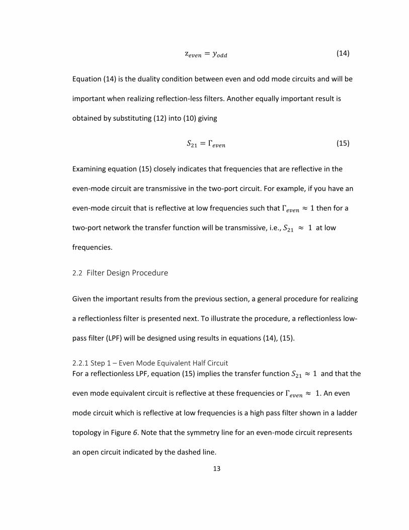
2.2.1 Step 1 – Even Mode Equivalent Half Circuit
For a reflectionless LPF, equation (15) implies the transfer function 𝑆21 ≈ 1 and that the
even mode equivalent circuit is reflective at these frequencies or Г𝑒𝑣𝑒𝑛 ≈ 1. An even
mode circuit which is reflective at low frequencies is a high pass filter shown in a ladder
topology in Figure 6. Note that the symmetry line for an even-mode circuit represents
an open circuit indicated by the dashed line.
14
Even-ModeEquivalent Circuit
Odd-ModeEquivalent Circuit
Figure 6: Reflectionless design procedure: step 1
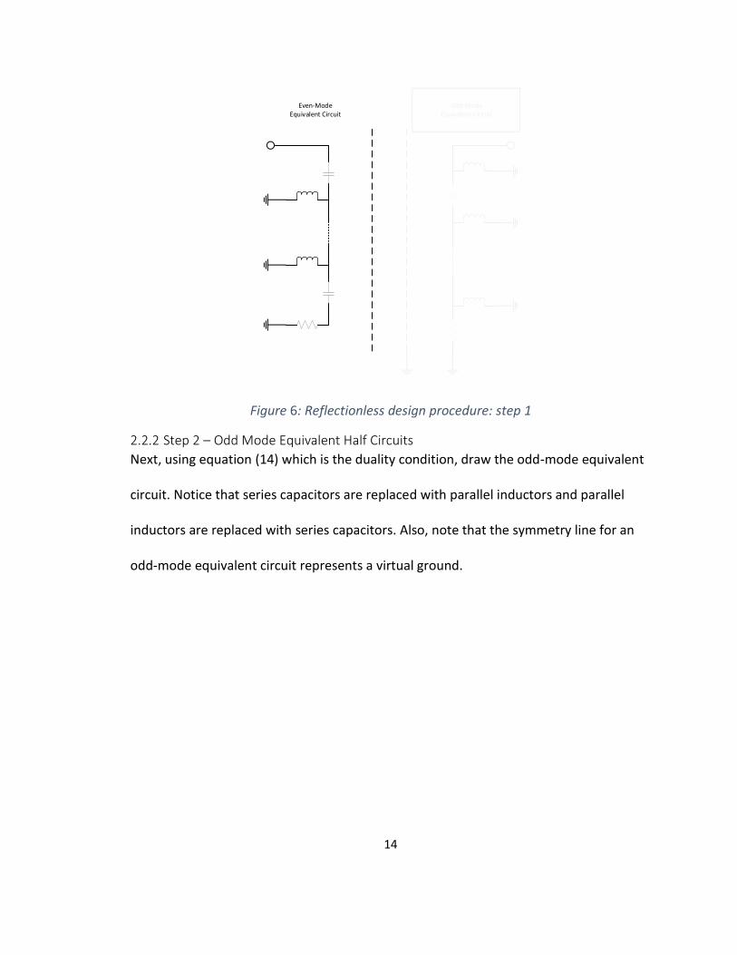
2.2.2 Step 2 – Odd Mode Equivalent Half Circuits
Next, using equation (14) which is the duality condition, draw the odd-mode equivalent
circuit. Notice that series capacitors are replaced with parallel inductors and parallel
inductors are replaced with series capacitors. Also, note that the symmetry line for an
odd-mode equivalent circuit represents a virtual ground.
15
Even-ModeEquivalent Circuit
Odd-ModeEquivalent Circuit
Figure 7: Reflectionless design procedure: step 2
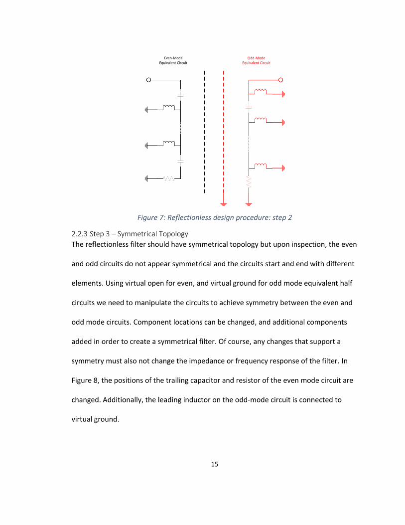
2.2.3 Step 3 – Symmetrical Topology
The reflectionless filter should have symmetrical topology but upon inspection, the even
and odd circuits do not appear symmetrical and the circuits start and end with different
elements. Using virtual open for even, and virtual ground for odd mode equivalent half
circuits we need to manipulate the circuits to achieve symmetry between the even and
odd mode circuits. Component locations can be changed, and additional components
added in order to create a symmetrical filter. Of course, any changes that support a
symmetry must also not change the impedance or frequency response of the filter. In
Figure 8, the positions of the trailing capacitor and resistor of the even mode circuit are
changed. Additionally, the leading inductor on the odd-mode circuit is connected to
virtual ground.
16
Even-ModeEquivalent Circuit
Odd-ModeEquivalent Circuit
Figure 8: Reflectionless design procedure: step 3a
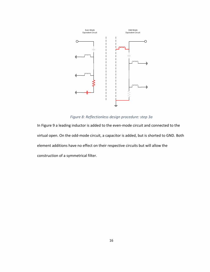
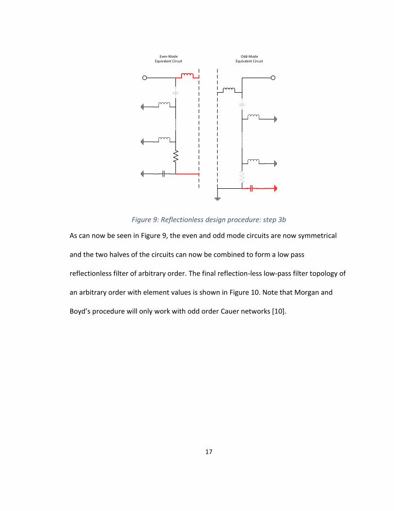
In Figure 9 a leading inductor is added to the even-mode circuit and connected to the
virtual open. On the odd-mode circuit, a capacitor is added, but is shorted to GND. Both
element additions have no effect on their respective circuits but will allow the
construction of a symmetrical filter.
17
Even-ModeEquivalent Circuit
Odd-ModeEquivalent Circuit
Figure 9: Reflectionless design procedure: step 3b
As can now be seen in Figure 9, the even and odd mode circuits are now symmetrical
and the two halves of the circuits can now be combined to form a low pass
reflectionless filter of arbitrary order. The final reflection-less low-pass filter topology of
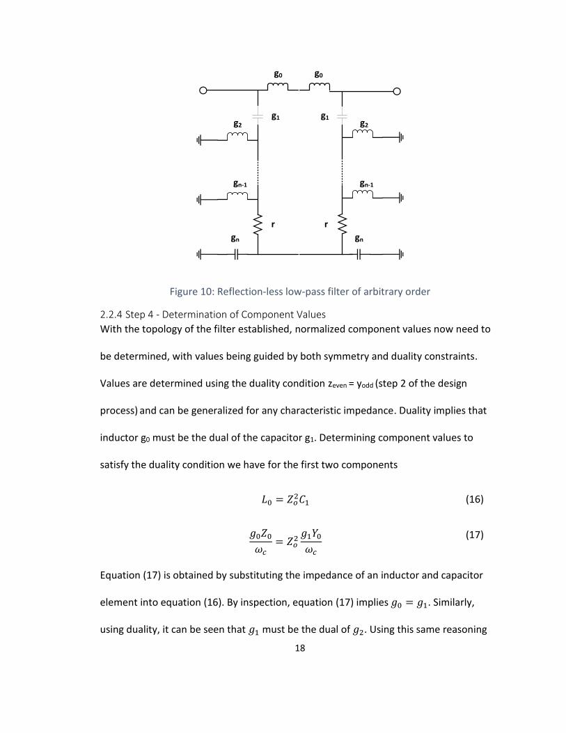
an arbitrary order with element values is shown in Figure 10. Note that Morgan and
Boyd’s procedure will only work with odd order Cauer networks [10].
18
g0 g0
g1 g1g2 g2
gn-1 gn-1
gn gn
rr
Figure 10: Reflection-less low-pass filter of arbitrary order
2.2.4 Step 4 - Determination of Component Values
With the topology of the filter established, normalized component values now need to
be determined, with values being guided by both symmetry and duality constraints.
Values are determined using the duality condition zeven = yodd (step 2 of the design
process) and can be generalized for any characteristic impedance. Duality implies that
inductor g0 must be the dual of the capacitor g1. Determining component values to
satisfy the duality condition we have for the first two components
𝐿0 = 𝑍𝑜2𝐶1 (16)
𝑔0𝑍0
𝜔𝑐= 𝑍𝑜
2𝑔1𝑌0
𝜔𝑐
(17)
Equation (17) is obtained by substituting the impedance of an inductor and capacitor
element into equation (16). By inspection, equation (17) implies 𝑔0 = 𝑔1. Similarly,
using duality, it can be seen that 𝑔1 must be the dual of 𝑔2. Using this same reasoning
19
we can infer 𝑔0 = 𝑔1 … = ⋯ 𝑔𝑘 and r=1 [10]. Thus, we can assign all the components a
value of unity without loss of generality.
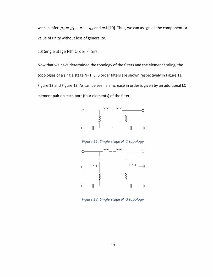
2.3 Single Stage Nth Order Filters
Now that we have determined the topology of the filters and the element scaling, the
topologies of a single stage N=1, 3, 5 order filters are shown respectively in Figure 11,
Figure 12 and Figure 13. As can be seen an increase in order is given by an additional LC
element pair on each port (four elements) of the filter.
Figure 11: Single stage N=1 topology
Figure 12: Single stage N=3 topology
20
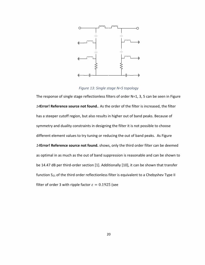
Figure 13: Single stage N=5 topology
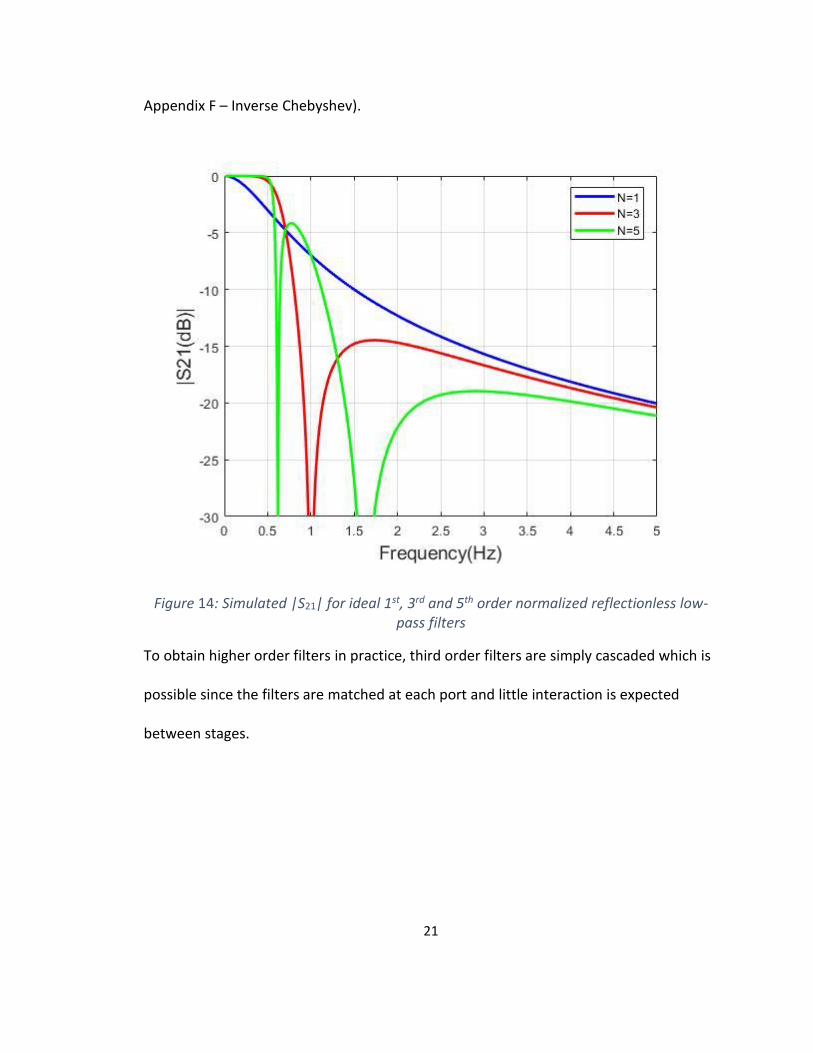
The response of single stage reflectionless filters of order N=1, 3, 5 can be seen in Figure
14Error! Reference source not found.. As the order of the filter is increased, the filter
has a steeper cutoff region, but also results in higher out of band peaks. Because of
symmetry and duality constraints in designing the filter it is not possible to choose
different element values to try tuning or reducing the out of band peaks. As Figure
14Error! Reference source not found. shows, only the third order filter can be deemed
as optimal in as much as the out of band suppression is reasonable and can be shown to
be 14.47 dB per third-order section [1]. Additionally [10], it can be shown that transfer
function S21 of the third order reflectionless filter is equivalent to a Chebyshev Type II
filter of order 3 with ripple factor 𝜀 = 0.1925 (see
21
Appendix F – Inverse Chebyshev).
Figure 14: Simulated |S21| for ideal 1st, 3rd and 5th order normalized reflectionless low-pass filters
To obtain higher order filters in practice, third order filters are simply cascaded which is
possible since the filters are matched at each port and little interaction is expected
between stages.

22
Chapter 3: Reflectionless Filter Realization - Simulation
Using the procedure described in chapter 2 this section will describe the design and
simulation of both ideal and non-ideal filters based on the design constraints outlined in
Morgan and Boyd’s paper.
3.1 Design of Ideal Filter
Morgan and Boyd’s paper outlines an anti-aliasing lowpass filter with the design
parameters shown in Table 1.
Table 1: Anti-aliasing filter design requirements
3dB Bandwidth 188MHz
Out of Band - alias Suppression 60 dB
The 3dB bandwidth requirement will determine the L, C component values required to
meet this specification. Each 3rd order section of the filter has a stopband rejection of
14.7 dB, so to meet the 60dB anti-alias suppression, four cascaded 3rd order sections will
be necessary to meet this requirement. Filter element values for the lowpass filter can
be determined directly from equations (18), (19) and (20) given by Morgan and Boyd
when designing for the pole frequency (𝜔𝑝)
𝐿 = 𝑍𝑜/𝜔𝑝 (18)
𝐶 = 𝑌𝑜/𝜔𝑝 (19)

23
𝑅 = 𝑍𝑜 (20)
However, it is often not useful to design a filter for the pole frequency; instead, a 3dB,
1dB or stopband frequency is specified. Because the 3rd order reflectionless filter
transfer function S21 is identically an inverse Chebyshev, this relationship can be used to
scale the filter to the appropriate target frequency see
24
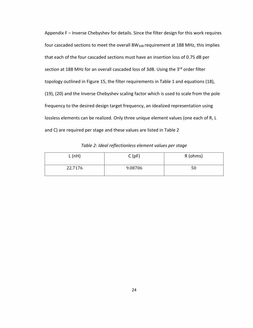
Appendix F – Inverse Chebyshev for details. Since the filter design for this work requires
four cascaded sections to meet the overall BW3dB requirement at 188 MHz, this implies
that each of the four cascaded sections must have an insertion loss of 0.75 dB per
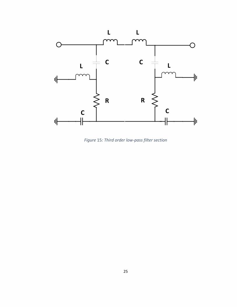
section at 188 MHz for an overall cascaded loss of 3dB. Using the 3rd order filter
topology outlined in Figure 15, the filter requirements in Table 1 and equations (18),
(19), (20) and the Inverse Chebyshev scaling factor which is used to scale from the pole
frequency to the desired design target frequency, an idealized representation using
lossless elements can be realized. Only three unique element values (one each of R, L
and C) are required per stage and these values are listed in Table 2
Table 2: Ideal reflectionless element values per stage
L (nH) C (pF) R (ohms)
22.7176 9.08706 50
25
L L
L LC C
C C
R R
Figure 15: Third order low-pass filter section
26
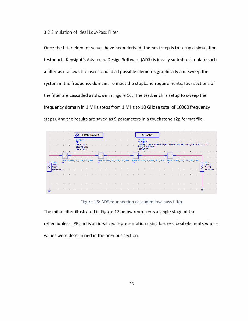
3.2 Simulation of Ideal Low-Pass Filter
Once the filter element values have been derived, the next step is to setup a simulation
testbench. Keysight’s Advanced Design Software (ADS) is ideally suited to simulate such
a filter as it allows the user to build all possible elements graphically and sweep the
system in the frequency domain. To meet the stopband requirements, four sections of
the filter are cascaded as shown in Figure 16. The testbench is setup to sweep the
frequency domain in 1 MHz steps from 1 MHz to 10 GHz (a total of 10000 frequency
steps), and the results are saved as S-parameters in a touchstone s2p format file.
Figure 16: ADS four section cascaded low-pass filter
The initial filter illustrated in Figure 17 below represents a single stage of the
reflectionless LPF and is an idealized representation using lossless ideal elements whose
values were determined in the previous section.
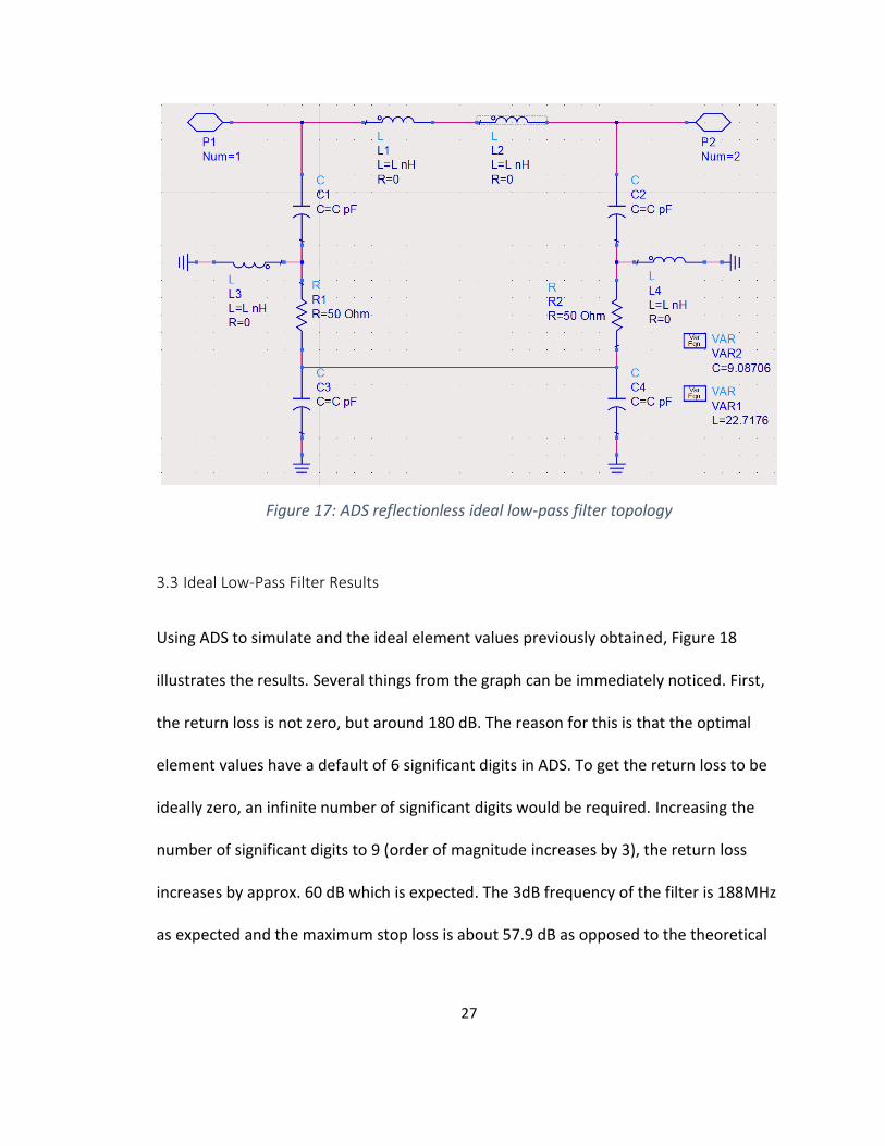
27
Figure 17: ADS reflectionless ideal low-pass filter topology
3.3 Ideal Low-Pass Filter Results
Using ADS to simulate and the ideal element values previously obtained, Figure 18
illustrates the results. Several things from the graph can be immediately noticed. First,
the return loss is not zero, but around 180 dB. The reason for this is that the optimal
element values have a default of 6 significant digits in ADS. To get the return loss to be
ideally zero, an infinite number of significant digits would be required. Increasing the
number of significant digits to 9 (order of magnitude increases by 3), the return loss
increases by approx. 60 dB which is expected. The 3dB frequency of the filter is 188MHz
as expected and the maximum stop loss is about 57.9 dB as opposed to the theoretical
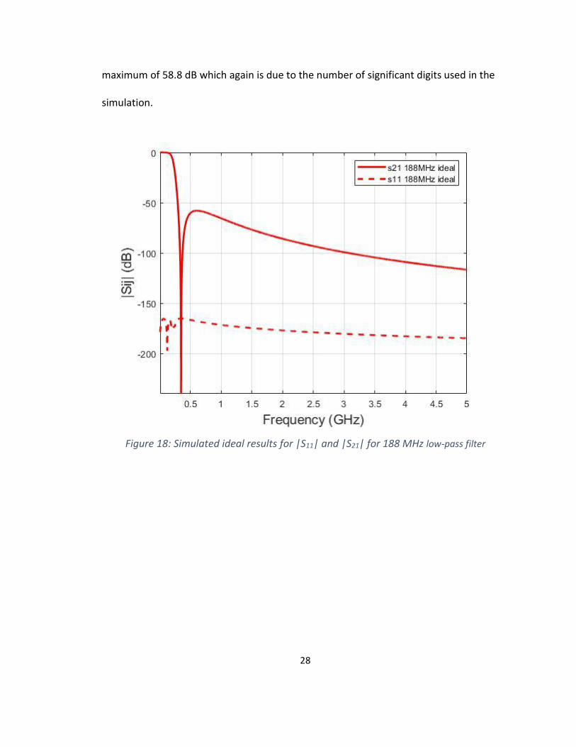
28
maximum of 58.8 dB which again is due to the number of significant digits used in the
simulation.
Figure 18: Simulated ideal results for |S11| and |S21| for 188 MHz low-pass filter
29
3.4 Simulation of Non-ideal Filter
The previous section simulated an ideal filter with both ideal components and lossless
transmission lines and showed good agreement with Morgan and Boyd’s results. To
more accurately simulate the filter to be realized, both the lossy nature of the PCB
materials, and the non-ideal nature of the filter components need to be considered.
Using ADS software, a more robust simulation can be realized where the lossy material
properties of the PCB and the microstrip transmission lines are included.
3.4.1 Non-ideal Components
Accurate models of multiple vendor passive components can be obtained from the
Modelithics EXEMPLAR Library [13]. These library parts have several parameters which
allow a range of values for substrate material dielectric and thickness, component
values and pad sizes. Depending on the Sim_mode and Pad_mode settings chosen at
simulation time, different pad or component parasitics will be included in the
simulation. For all final simulations presented in this work (sim_mode, pad_mode) =
(0,0) was chosen so that a full simulation including pad, parasitics and dielectric effects
was performed. The components packages chosen for this work were either 0402 or
0603 standard surface mount passives. The smaller component package sizes were
chosen as in general smaller packages have smaller parasitic effects. See Appendix D –
Simulation Library for more information regarding the Modelithics library and the pads.
30
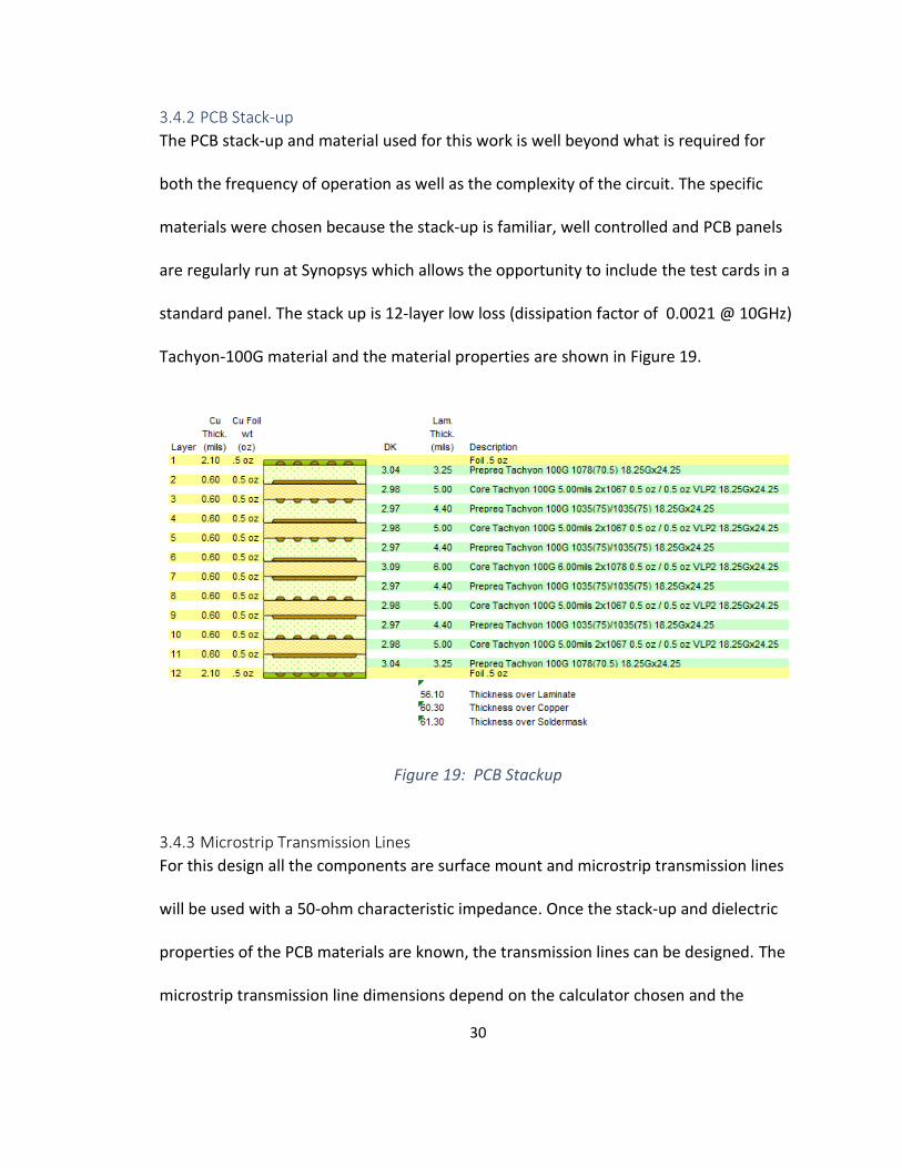
3.4.2 PCB Stack-up
The PCB stack-up and material used for this work is well beyond what is required for
both the frequency of operation as well as the complexity of the circuit. The specific
materials were chosen because the stack-up is familiar, well controlled and PCB panels
are regularly run at Synopsys which allows the opportunity to include the test cards in a
standard panel. The stack up is 12-layer low loss (dissipation factor of 0.0021 @ 10GHz)
Tachyon-100G material and the material properties are shown in Figure 19.
Figure 19: PCB Stackup
3.4.3 Microstrip Transmission Lines
For this design all the components are surface mount and microstrip transmission lines
will be used with a 50-ohm characteristic impedance. Once the stack-up and dielectric
properties of the PCB materials are known, the transmission lines can be designed. The
microstrip transmission line dimensions depend on the calculator chosen and the
31
author’s experience with the material, stackup and fabrication facilities. For this design a
50-ohm microstrip transmission line was determined to be 6 mils in width given the PCB
material properties. Additional information regarding microstrip transmission lines in
addition to the calculator used are in Appendix D – Simulation Library.
3.4.4 ADS Non-ideal Testbench
Pulling all the non-ideal components into ADS, the testbench now includes lossy PCB
effects, lossy transmission lines, non-ideal components and component parasitics. As in
the ideal testbench case, the simulation is swept from 1 MHz to 10GHz in 1 MHz steps.
The component values used are no longer the ideal theoretical values but what is
available for the component families chosen. For this work, the component families
were from available libraries of the Modelithics software and which were available to be
purchased and are shown in Table 3 with the comparative ideal values.
Table 3: Reflectionless 188MHz component values
L (nH) C (pF) R (ohms)
Ideal 22.7176 9.08706 50
Non-ideal (5%) 23 9.1 49.9

32
The representation of a single stage of the filter is given in Figure 20 which includes the
microstrip transmission lines, component pad effects and vias. The vias used were ADS
library vias and represented the barrel and pad dimensions of the via callouts in the
layout.
Figure 20: ADS non-ideal filter section

33
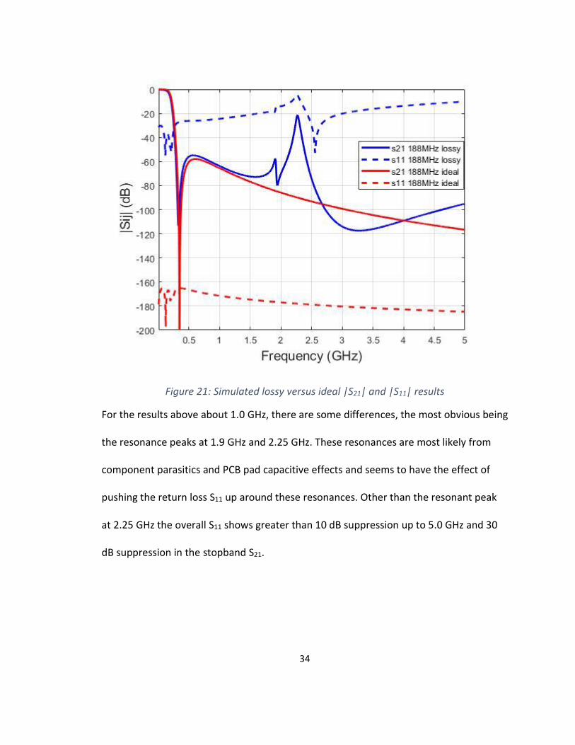
3.5 Comparing Ideal and Non-Ideal Simulated Filter Results
To get an idea of the effects of non-ideal components and lossy PCB materials, the S-
parameter results of both lossy and ideal reflectionless filter simulations are shown in
Figure 21. Note that all measured results shown in this work have been de-embedded
from the SMA launches – see Appendix C - Automatic Fixture Removal (AFR).
The Morgan and Boyd paper showed results up to 1.0 GHz, but for this work the
bandwidth has been expanded to 5 GHz to see what effects occur above the immediate
passband frequency. Firstly, the general shape of the results below 1.0 GHz is very
similar between the two plots although as can be seen the return loss (S11) is much more
sensitive to the effects of non-ideal components and a lossy PCB. The Insertion Loss (S21)
is slightly higher below 1.0 GHz due to copper, dielectric losses and skin effect.
34
Figure 21: Simulated lossy versus ideal |S21| and |S11| results
For the results above about 1.0 GHz, there are some differences, the most obvious being
the resonance peaks at 1.9 GHz and 2.25 GHz. These resonances are most likely from
component parasitics and PCB pad capacitive effects and seems to have the effect of
pushing the return loss S11 up around these resonances. Other than the resonant peak
at 2.25 GHz the overall S11 shows greater than 10 dB suppression up to 5.0 GHz and 30
dB suppression in the stopband S21.
35
Chapter 4: Filter Realization – Fabrication
In order to appraise the validity of the simulation results, a filter must be fabricated, and
the frequency response measured in the lab. The design and fabrication process of the
reflectionless filter designated the Device Under test (DUT) is outlined in the following
sections.
4.1 PCB Schematic Design
Once the simulations have been completed and the results deemed acceptable, the first
step in fabricating the filter is to create a netlist with associated component footprints
and the software chosen to generate the netlist was Allegro Orcad Schematic Capture. A
generalized component layout of each stage of the filter can be gleaned from the ADS
testbench representation of a single stage of the ideal filter. The DUT will require four
identical cascaded single stages. To evaluate and measure the filter performance over
frequency a Vector Network Analyzer (VNA) will be the equipment of choice and the
VNA interfaces to the DUT via SMA connectors. The DUT is a two-port device, which
requires that the test card must have two SMA ports to allow for proper stimulation by
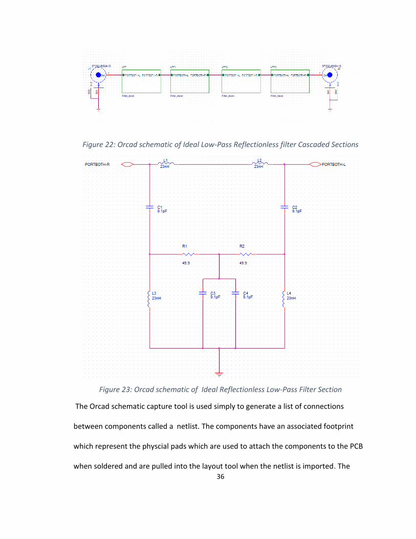
the VNA. Figure 22 and Figure 23 illustrate the Orcad hierarchical schematic
representation of the cascaded stages making up the complete filter.
36
Figure 22: Orcad schematic of Ideal Low-Pass Reflectionless filter Cascaded Sections
Figure 23: Orcad schematic of Ideal Reflectionless Low-Pass Filter Section
The Orcad schematic capture tool is used simply to generate a list of connections
between components called a netlist. The components have an associated footprint
which represent the physcial pads which are used to attach the components to the PCB
when soldered and are pulled into the layout tool when the netlist is imported. The

37
component values in the schematic are the same as in Table 3 but other than allowing a
bill of materials (BOM) to be created, the component values have no other function.
38
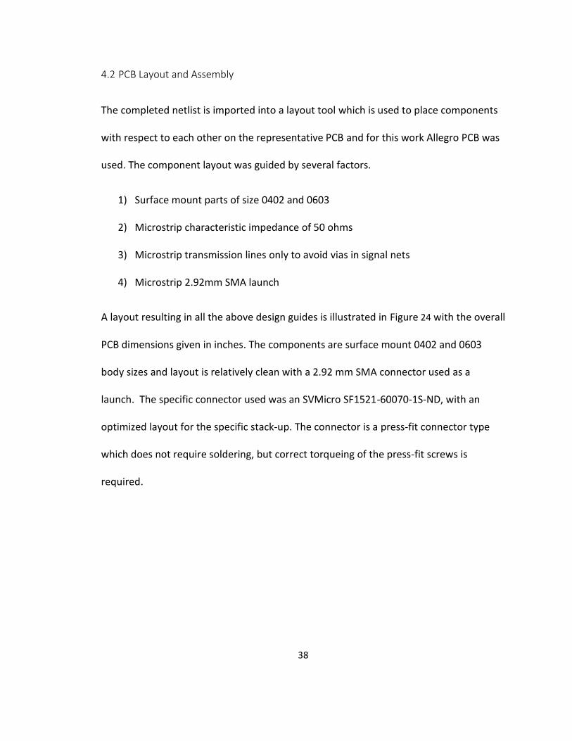
4.2 PCB Layout and Assembly
The completed netlist is imported into a layout tool which is used to place components
with respect to each other on the representative PCB and for this work Allegro PCB was
used. The component layout was guided by several factors.
1) Surface mount parts of size 0402 and 0603
2) Microstrip characteristic impedance of 50 ohms
3) Microstrip transmission lines only to avoid vias in signal nets
4) Microstrip 2.92mm SMA launch
A layout resulting in all the above design guides is illustrated in Figure 24 with the overall
PCB dimensions given in inches. The components are surface mount 0402 and 0603
body sizes and layout is relatively clean with a 2.92 mm SMA connector used as a
launch. The specific connector used was an SVMicro SF1521-60070-1S-ND, with an
optimized layout for the specific stack-up. The connector is a press-fit connector type
which does not require soldering, but correct torqueing of the press-fit screws is
required.
39
Figure 24: Reflectionless PCB layout
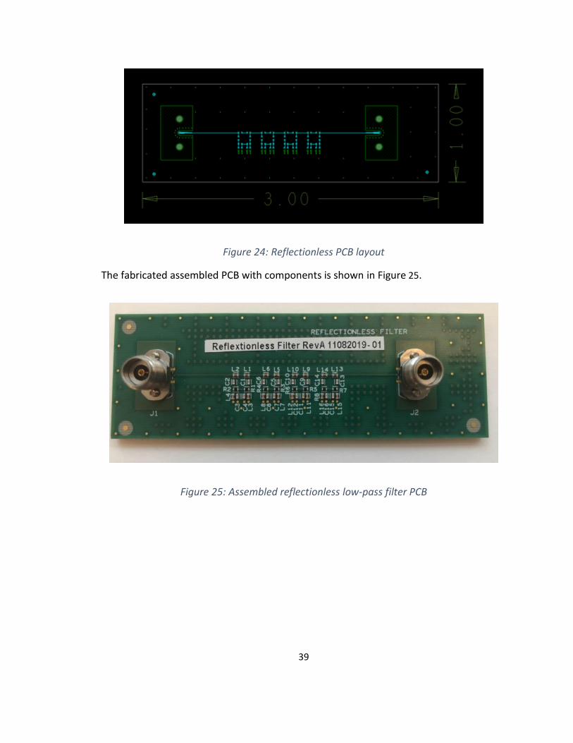
The fabricated assembled PCB with components is shown in Figure 25.
Figure 25: Assembled reflectionless low-pass filter PCB
40
4.3 Butterworth Diplexer
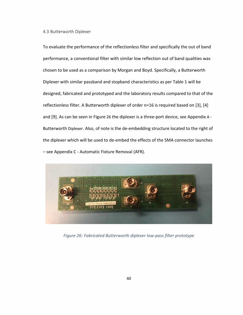
To evaluate the performance of the reflectionless filter and specifically the out of band
performance, a conventional filter with similar low reflection out of band qualities was
chosen to be used as a comparison by Morgan and Boyd. Specifically, a Butterworth
Diplexer with similar passband and stopband characteristics as per Table 1 will be
designed, fabricated and prototyped and the laboratory results compared to that of the
reflectionless filter. A Butterworth diplexer of order n=16 is required based on [3], [4]
and [9]. As can be seen in Figure 26 the diplexer is a three-port device, see Appendix A -
Butterworth Diplexer. Also, of note is the de-embedding structure located to the right of
the diplexer which will be used to de-embed the effects of the SMA connector launches
– see Appendix C - Automatic Fixture Removal (AFR).
Figure 26: Fabricated Butterworth diplexer low-pass filter prototype

41
Chapter 5: Experimental Results
In the Chapter 3 a reflectionless low-pass filter was designed and simulated in ADS with
simulation results showing good agreement with Morgan and Boyd’s published results.
In Chapter 4 a physical prototype of the same filter was realized, fabricated and
assembled. To further confirm the Morgan and Boyd’s reflectionless theory, the
prototypes must be measured and compared to simulated data and to theory.
To do a direct comparison between the ADS simulated results and the lab measured
results, the PCB SMA launches must be de-embedded from the measurements and then
the de-embedded measured results compared to simulation results. The de-embedding
is an important step as no SMA model was obtained from the manufacturer, so no
simulation could be run in ADS which would include the SMA connector effects which
would be cumulative with the filter response. As can be seen in the ADS hierarchical
schematic in Figure 16, no connector model was included in the simulation and the filter
was terminated with ideal 50 ohm terminations at each port. Any measured results
presented in this work will only be with the SMA launches de-embedded unless
specifically noted. Appendix C - Automatic Fixture Removal gives more details regarding
this de-embedding procedure.
To measure the filter response a Keysight N5227B PNA Microwave Network Analyzer
[14] is the preferred equipment of choice. Before any measurements were undertaken,
the VNA was calibrated using a standard SOLT calibration procedure – see Appendix B -
42
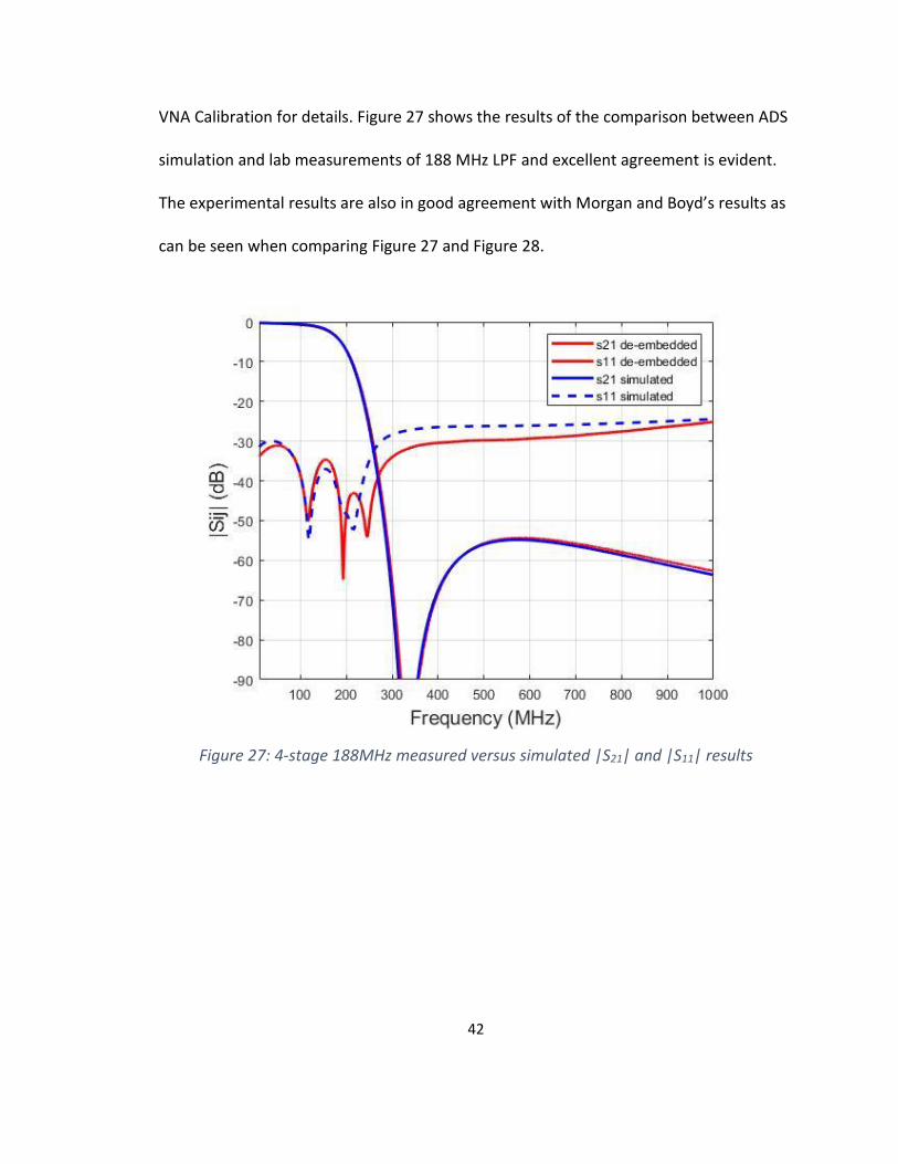
VNA Calibration for details. Figure 27 shows the results of the comparison between ADS
simulation and lab measurements of 188 MHz LPF and excellent agreement is evident.
The experimental results are also in good agreement with Morgan and Boyd’s results as
can be seen when comparing Figure 27 and Figure 28.
Figure 27: 4-stage 188MHz measured versus simulated |S21| and |S11| results
43
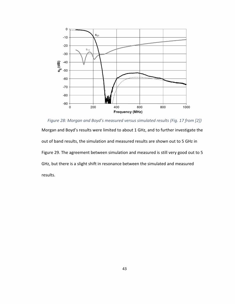
Figure 28: Morgan and Boyd’s measured versus simulated results (Fig. 17 from [2])
Morgan and Boyd’s results were limited to about 1 GHz, and to further investigate the
out of band results, the simulation and measured results are shown out to 5 GHz in
Figure 29. The agreement between simulation and measured is still very good out to 5
GHz, but there is a slight shift in resonance between the simulated and measured
results.
44
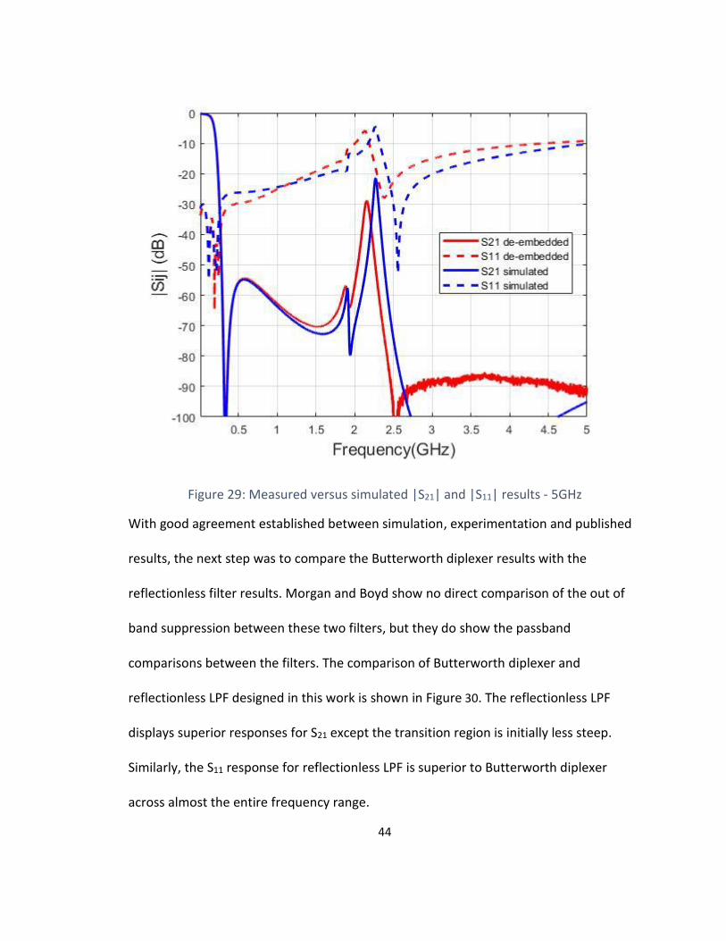
Figure 29: Measured versus simulated |S21| and |S11| results - 5GHz
With good agreement established between simulation, experimentation and published
results, the next step was to compare the Butterworth diplexer results with the
reflectionless filter results. Morgan and Boyd show no direct comparison of the out of
band suppression between these two filters, but they do show the passband
comparisons between the filters. The comparison of Butterworth diplexer and
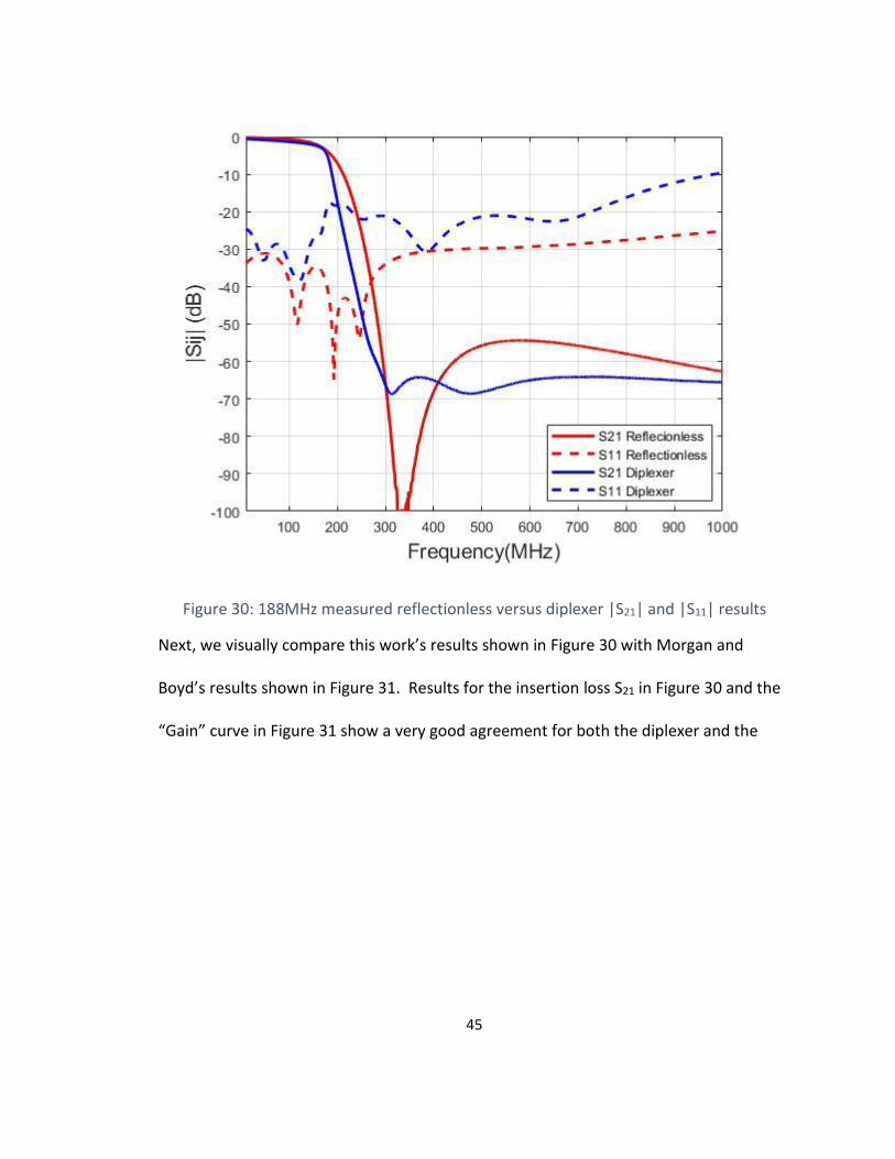
reflectionless LPF designed in this work is shown in Figure 30. The reflectionless LPF
displays superior responses for S21 except the transition region is initially less steep.
Similarly, the S11 response for reflectionless LPF is superior to Butterworth diplexer
across almost the entire frequency range.
45
Figure 30: 188MHz measured reflectionless versus diplexer |S21| and |S11| results
Next, we visually compare this work’s results shown in Figure 30 with Morgan and
Boyd’s results shown in Figure 31. Results for the insertion loss S21 in Figure 30 and the
“Gain” curve in Figure 31 show a very good agreement for both the diplexer and the
46
reflectionless filter. This agreement also confirms that our diplexer design and
implementation is very close to that reported by Morgan and Boyd.
Figure 31: Morgan and Boyd’s diplexer versus reflectionless results (Fig. 12 from [2])
Another important feature of the reflectionless filter is the symmetry property. The
filter is a two-port device and because of symmetry the return loss at both ports is
theoretically identical. This allows these filters to be cascaded with other filters or with
other sensitive 50-ohm components with little interaction. Figure 32 demonstrates that
reflectionless filter indeed has symmetrical response and that both ports S11 and S22
have very close to symmetrical return loss. Without the resonance at 2.25 GHz the
reflectionless filter would have S11 better than 10 dB out to 5 GHz. The diplexer is

47
matched for S11 (common port) relatively well but S22 shows almost unity reflection in
the stop band. Any noise above the passband frequency on diplexer port 2 will tend to
reflect from the filter back to the load rather than being absorbed with possible
resonance ramifications between the filter and any connected circuits.
Figure 32: 188MHz measured reflectionless versus diplexer return loss |S11| and |S22| results

48
5.1 Frequency Scaling
Morgan and Boyd’s results were for a 188MHz Low Pass filter and as such the frequency
range of interest was up to 1 GHz. To investigate the response of the reflectionless filter
topology to higher frequencies, the original filter design 3dB bandwidth was increased
by a decade to 1.88 GHz. Of specific interest was how well the return loss would behave
out to 10 GHz. As with any of the classical filters, the reflectionless filter can be scaled
using standard scaling techniques. The simulated and measured results for this
frequency scaling are shown in Figure 33 . The measured and simulated responses show
very good agreement up to 10 GHz.
49
Figure 33: Reflectionless 1.88GHz LPF measured versus simulated |S21| and |S11|results
There are two notable resonances in the measured S21 response at 5.75 GHz and 6.65
GHz. They are approximately 25 dB suppressed in the stop band, but they seem to have
an effect of pushing the Return loss to above 5dB. A possible reason for this could be a
component package or pad resonance effect.
To further compare the response quality of the scaled reflectionless filter, a scaled
Butterworth diplexer was also designed and measured in the lab with the responses
compared in Figure 34. The reflectionless filter shows overall about a 10-dB

50
improvement in S11 in the stopband region compared to the diplexer but has higher
mismatch at lower (less than 500 MHz) frequencies which was confirmed in simulation.
Figure 34: 1.88 GHz measured de-embedded reflectionless vs diplexer |S21| and |S11| results
51
Chapter 6: Discussion, Conclusions and Future Work
6.1 Discussion
The basic undertaking of this work was conceptually relatively straight forward. Firstly,
we set out to understand Morgan and Boyd’s reflectionless filer design procedure.
Secondly, we verified the results of this procedure by measuring realized filter
prototypes in the lab. In the process of this work several unexpected issues arose while
other issues that at first were expected to be difficult proved to be simpler than
originally anticipated.
The procedure outlined by Morgan and Boyd to design a reflectionless filter required
some knowledge of duality, symmetry and even-odd mode analysis. Using the preceding
theory and stepping through the procedure was relatively intuitive as presented by
Morgan and Boyd. The design of the diplexer turned out to be more of a challenge
conceptually. With common filter parameters defined for both filters and the
component values designed initially on spreadsheets, the next step was to run
simulations of the resulting filters. Using ADS, simulations were run on ideal filters of
both types to confirm the desired attributes (3dB bandwidth, stopband attenuation).
The next step was to add non-ideal components and lossy PCB materials. One of the
advantages of the reflectionless filter that became very apparent early in the design
process was the much smaller number of unique components required to construct the
filter when compared to the analogous Butterworth diplexer. For the reflectionless
52
filters in this work, there were three unique component values (one each of L, C, R)
required versus fully 32 unique component values for the similar Diplexer filter. Because
so many unique component values were required for the diplexer and given that there
are only a limited number of available component values, some of the component
values chosen for diplexer differed by more than five percent from their theoretical
values. The element values chosen were confined to be from family simulation libraries
available in Modelithics and from components that were readily obtainable. Given more
time and effort, components with less than 5% deviation from the ideal might have
been obtained.
The parasitic effects of the components were not unexpected but the accuracy of the
simulations in showing these effects using the Modelithics models resulted in the
simulation and measured results matching very well for all filters. The primary parasitic
effect was the component pad capacitance, which unfortunately was exacerbated by
the chosen stackup. The stackup used is of a much higher quality than is required for the
frequency range used in this work and was chosen because of the author’s familiarity
and access to the material. The number of layers in the stackup was 12, but this specific
work only requires a standard two-layer stackup as the components used were surface
mount and the transmission lines were microstrip located on the top layer only. Because
of this, only the top two layers of the stackup were used with the second layer being
used as the microstrip reference. This means that the dielectric thickness of only 3mils is
present between the microstrip and the reference plane. This relative thinness of the
53
dielectric material exacerbated the parasitic pad caps of the components. For example,
to obtain a 50-ohm microstrip impedance with this dielectric material and thickness, a 6
mil microstrip line was required. The pads for the 0402 components were approximately
20 mils square. By just increasing the thickness of the dielectric from 3 to 30 mils the
parasitic capacitance would decrease by a factor of 10.
The 3-dB frequency of the reflectionless filter - both measured and simulated - was
172MHz but the initial target frequency was 188MHz using ideal components and no
PCB effects. This lower frequency was not an unexpected result due to the lossy nature
of the PCB and the components and the precision of the components which was 5%.
The reflectionless filter was scaled using standard frequency scaling techniques and
compared to a similarly scaled Butterworth diplexer. The scaled reflectionless filter was
found to have good return loss over the measured frequency range and was comparable
to the Butterworth diplexer.
Because of symmetry, the reflectionless filter showed good return loss at both ports
across all frequencies investigated. Also, the return loss of the reflectionless filter in the
stopband was superior to the diplexer over all frequencies investigated. Additionally,
the diplexer only had good return loss characteristics at the common port whereas the
other ports had poor return loss which precluded the diplexer from being cascaded. The
symmetry of the ports of the reflectionless filter is one of its best features which allows

54
the filter or multiple reflectionless filters to be inserted in circuits without interacting
unpredictably with circuit elements on either port.
6.2 Conclusion
The main goals of this work to validate and to verify the novel filter design procedure
outlined in Morgan and Boyd’s paper were achieved and a low pass reflectionless filter
prototype was realized. A classical complimentary Butterworth diplexer prototype was
also realized and used to evaluate the quality of the return loss characteristics for the
reflectionless filter. The filter prototype measurement results obtained for both filters
show the reflectionless has improved return loss characteristics to the diplexer over a
wide frequency range.
In summary, this work addressed
• reflectionless filter design procedure
• frequency scaling property of reflectionless filters
• good matching between simulation and measured response for reflectionless
filters
• return loss of both ports on reflectionless filter were superior to classical design
6.3 Future Work
This work was an introduction into reflectionless filters and allowed for the replication,
verification, and frequency extension of Morgan and Boyd’s novel ideas. However,
55
several additional areas of investigation could be done which could build directly on this
work.
1. Determining the sensitivity of component values in reflectionless filters would
allow the designer to specify the tolerance of values that could be used in a filter
without radically changing the performance of the filter.
2. Minimizing the effects of the parasitic pad capacitance could be done in several
ways. The first method would be a direct continuation of this work and would
use the same substrate and materials. The idea would be that the reference
plane directly beneath the component and pads would be voided and as a result,
the reference layer would then become one of the deeper layers. This would
have the effect of increasing the dielectric thickness and decreasing the parasitic
pad capacitance. However additional GND vias surrounding the component
would be needed to tie the reference planes. The second method would be to
use a standard two-layer PCB and simply the increased thickness of the dielectric
material would mitigate some of the pad capacitance effects.
3. Investigating how high in frequency one can push these filters when using
discrete components. The component values will scale with frequency but most
likely a different family of components will need to be used.
4. Use a prototype in a system which has a source that is sensitive to out of band
reflections and determine if the interaction is mitigated by using a reflectionless
filter [15].

56
5. Cascade multiple reflectionless filters such as a low pass and a high pass to
obtain a bandpass filter to demonstrate the ability of the reflectionless filter
topology to allow concatenation of filters [16].
57
References
[1] M. Morgan, “Think Outside the Band”, IEEE Microwave Magazine, pp 54-62,
November/December 2018.
[2] Matthew A. Morgan and Tod A. Boyd, “Technical and experimental study of a
new class of reflectionless filter”, IEEE Transactions on Microwave Theory and
Techniques, Vol 59, No 5, pp 1214-1221, May 2011. DOI
10.1109/TMTT.2011.2113189
[3] G. L Matthaei and E. G. Cristal, “Theory and Design of Diplexers and
Multiplexers”, Advances in Microwaves, Vol. 2, pp 237-326, 1967
[4] R. G Veltrop and R. B. Wilds, “Modified Tables for the Design of Optimum
Diplexers”, Electronic Defense Laboratories, Technical Memorandum, No EDL-
M559, 3 July 1963
[5] E. A. Guillemin, “Synthesis of Passive Networks”, New York: J Wiley, 1957
[6] V. Met, “Absorptive filters for Microwave Harmonic Power”, Proc, IRE, 1959, 47,
(10), pp. 1762-1769. DOI 11.1109/JRPROC.1959.287111
[7] H. W. Bode, “Network Analysis and Feedback Amplifier Design” New York: D. Van
Nostrand Company, 1945.
[8] Senad Bulja, Andrei Grebennikov, Pawel Rulikowski, “Theory, analysis and design
of high order reflective, absorptive filters”, IET Microwaves, Antennas and
Propagation, March 2017. DOI 10.1049/iet-map.2016.0431
[9] G. Matthaei, L. Young, and E. Jones, “Microwave Filters, Impedance Matching
Networks, and Coupling Structures”. Norwood, MA: Artech House, 1980
[10] Matthew A Morgan, “Reflectionless Filters”, Norwood MA: Artech House, 2017
[11] C Bowick, J Blyther and C Ajluni, “RF Circuit Design”, Burlington, MA, USA: Newnes, 2008, pp. 41
[12] A. C. Bartlett, “The Theory of Electrical Artificial Lines and Filters”. New York, NY,
USA: Wiley, 1930, pp. 28–32. [13] Modelithics Exemplar Library [online] Available: https://www.modelithics.com/
58
[14] Alexander Russell, “A Treatise on the Theory of Alternating Currents”, Vol. 1,
Chapter XX1, Cambridge: University Press, 1904
[15] A. Brizic and D. Babic, “Constant-resistance filters with diplexer architecture for
S-band applications,” MIPRO/MEET, pp 80-85, 2019. DOI
10.23919/MIPRO.2019.8756659
[16] Mini-Circuits Inc (2015). “Pairing mixers with reflectionless filters to improve
system performance”, [online] Available:
http://www.minicircuits.com/aap/AN75-07.pdf
[17] Peter A. Rizzi, “Microwave Engineering: Passive Circuits”, Prentice-Hall, 1988
59
Appendix A - Butterworth Diplexer
A diplexer is a passive device that implements frequency-domain multiplexing and can be used for dividing a broad frequency band into smaller bands using selective filters. It is fundamentally different from a passive combiner or splitter in that the ports are frequency selective. This separation of desired frequency bands, however, is a much more difficult task than appears at first sight. If filters are simply connected in a parallel manner, interaction between the inputs of each filter will degrade the overall performance of the diplexer unless the filters are carefully designed. For the purposes of this study, a dual diplexer formulation is considered where one constructs a low pass (passband) and high pass (stopband) filters to have complimentary input admittances and the filters are then connected in parallel. The input admittance of the diplexer is 𝑌𝑝 + 𝑌𝑠 where 𝑌𝑝 and 𝑌𝑠 represent the input admittances of the passband and stopband
filter respectively. A matched filter requires 𝑌𝑜 = 𝑌𝑝 + 𝑌𝑠 which means that the sum of
the input admittance of the lowpass and high pass filter is real and constant for all frequencies. Filter pairs that satisfy this condition are termed complimentary.
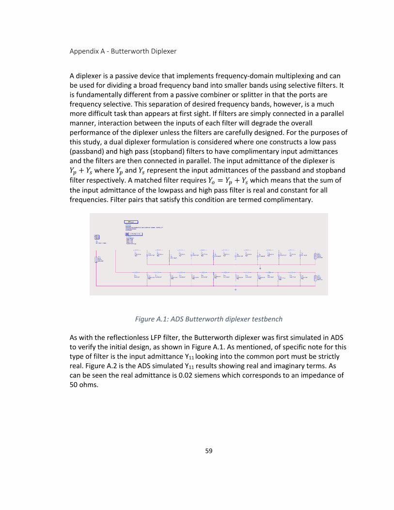
Figure A.1: ADS Butterworth diplexer testbench
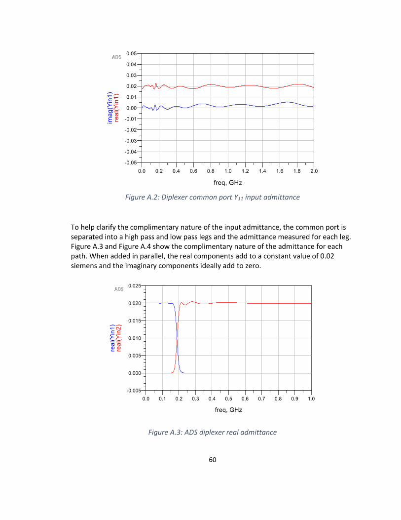
As with the reflectionless LFP filter, the Butterworth diplexer was first simulated in ADS to verify the initial design, as shown in Figure A.1. As mentioned, of specific note for this type of filter is the input admittance Y11 looking into the common port must be strictly real. Figure A.2 is the ADS simulated Y11 results showing real and imaginary terms. As can be seen the real admittance is 0.02 siemens which corresponds to an impedance of 50 ohms.
60
Figure A.2: Diplexer common port Y11 input admittance
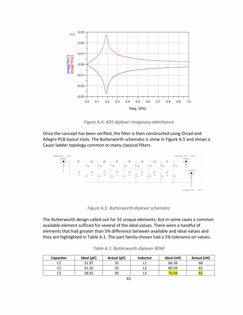
To help clarify the complimentary nature of the input admittance, the common port is separated into a high pass and low pass legs and the admittance measured for each leg. Figure A.3 and Figure A.4 show the complimentary nature of the admittance for each path. When added in parallel, the real components add to a constant value of 0.02 siemens and the imaginary components ideally add to zero.
Figure A.3: ADS diplexer real admittance
61
Figure A.4: ADS diplexer imaginary admittance
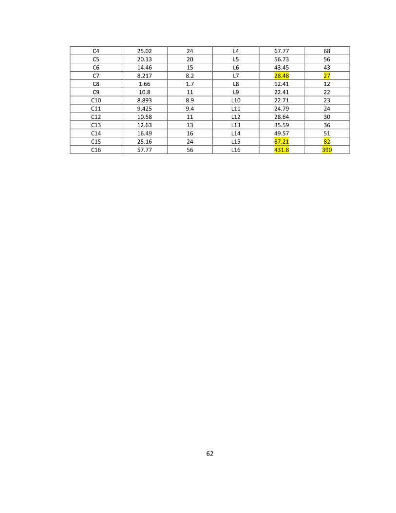
Once the concept has been verified, the filter is then constructed using Orcad and Allegro PCB layout tools. The Butterworth schematic is show in Figure A.5 and shows a Cauer ladder topology common to many classical filters.
Figure A.5: Butterworth diplexer schematic
The Butterworth design called out for 32 unique elements, but in some cases a common available element sufficed for several of the ideal values. There were a handful of elements that had greater than 5% difference between available and ideal values and they are highlighted in Table A.1. The part family chosen had a 5% tolerance on values.
Table A.1: Butterworth diplexer BOM
Capacitor Ideal (pF) Actual (pF) Inductor Ideal (nH) Actual (nH)
C1 31.97 33 L1 66.38 68
C2 31.56 33 L2 80.59 82
C3 28.92 30 L3 76.04 82
62
C4 25.02 24 L4 67.77 68
C5 20.13 20 L5 56.73 56
C6 14.46 15 L6 43.45 43
C7 8.217 8.2 L7 28.48 27
C8 1.66 1.7 L8 12.41 12
C9 10.8 11 L9 22.41 22
C10 8.893 8.9 L10 22.71 23
C11 9.425 9.4 L11 24.79 24
C12 10.58 11 L12 28.64 30
C13 12.63 13 L13 35.59 36
C14 16.49 16 L14 49.57 51
C15 25.16 24 L15 87.21 82
C16 57.77 56 L16 431.8 390
63
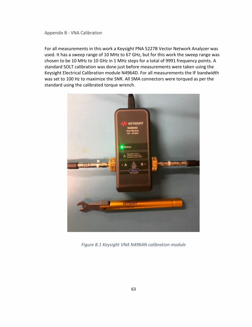
Appendix B - VNA Calibration
For all measurements in this work a Keysight PNA 5227B Vector Network Analyzer was used. It has a sweep range of 10 MHz to 67 GHz, but for this work the sweep range was chosen to be 10 MHz to 10 GHz in 1 MHz steps for a total of 9991 frequency points. A standard SOLT calibration was done just before measurements were taken using the Keysight Electrical Calibration module N4964D. For all measurements the IF bandwidth was set to 100 Hz to maximize the SNR. All SMA connectors were torqued as per the standard using the calibrated torque wrench.
Figure B.1 Keysight VNA N4964N calibration module
64
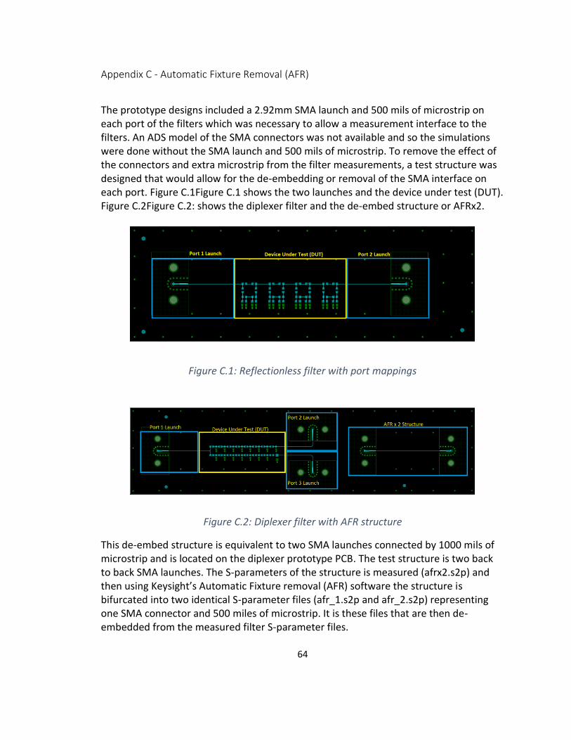
Appendix C - Automatic Fixture Removal (AFR)
The prototype designs included a 2.92mm SMA launch and 500 mils of microstrip on each port of the filters which was necessary to allow a measurement interface to the filters. An ADS model of the SMA connectors was not available and so the simulations were done without the SMA launch and 500 mils of microstrip. To remove the effect of the connectors and extra microstrip from the filter measurements, a test structure was designed that would allow for the de-embedding or removal of the SMA interface on each port. Figure C.1Figure C.1 shows the two launches and the device under test (DUT). Figure C.2Figure C.2: shows the diplexer filter and the de-embed structure or AFRx2.
Figure C.1: Reflectionless filter with port mappings
Figure C.2: Diplexer filter with AFR structure
This de-embed structure is equivalent to two SMA launches connected by 1000 mils of microstrip and is located on the diplexer prototype PCB. The test structure is two back to back SMA launches. The S-parameters of the structure is measured (afrx2.s2p) and then using Keysight’s Automatic Fixture removal (AFR) software the structure is bifurcated into two identical S-parameter files (afr_1.s2p and afr_2.s2p) representing one SMA connector and 500 miles of microstrip. It is these files that are then de-embedded from the measured filter S-parameter files.

65
Figure C.3: AFRx2 prototype
Figure C.4: AFRx2 S21
66
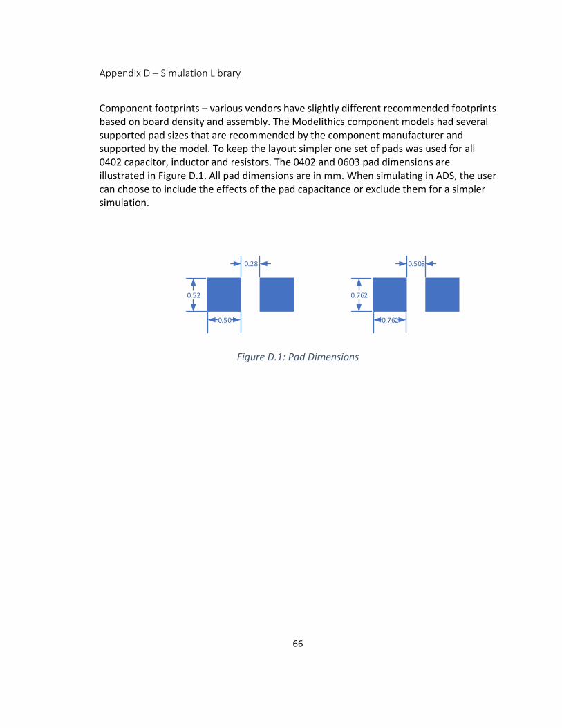
Appendix D – Simulation Library
Component footprints – various vendors have slightly different recommended footprints based on board density and assembly. The Modelithics component models had several supported pad sizes that are recommended by the component manufacturer and supported by the model. To keep the layout simpler one set of pads was used for all 0402 capacitor, inductor and resistors. The 0402 and 0603 pad dimensions are illustrated in Figure D.1. All pad dimensions are in mm. When simulating in ADS, the user can choose to include the effects of the pad capacitance or exclude them for a simpler simulation.
0.50
0.52
0.28
0.762
0.762
0.508
Figure D.1: Pad Dimensions

67
The system impedance is targeted at 50 ohms and given the layer thickness, dielectric constant the microstrip transmission line width can be determined. There is a plethora of calculators online and in software tools, and in this user’s experience many are erroneous or do not clearly state under what physical conditions they can be used. The calculator used was found at https://www.microwaves101.com/calculators/1201-microstrip-calculator and is based on David Campbell’s calculator.
t
h
w
Figure D.2: Microstrip calculator
Additionally, because the stackup and material are well known to this author, the microstrip width was known a-priori to be 6mils. The calculator gave 6.4 mils to achieve 50-ohm characteristic impedance.
Table D.1: PCB material properties
Microstrip Copper Thickness t (mils) 2.1
Dielectric height h (mils) 3.25
Dielectric constant ε 3.04
Microstrip Width w (mils) 6
Characteristic Impedance Zo (ohms) 50
Loss Tangent 0.0021
68
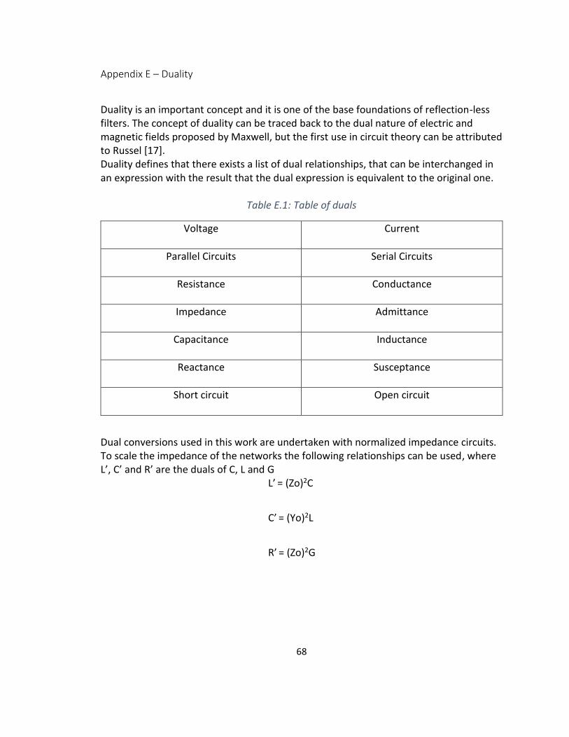
Appendix E – Duality
Duality is an important concept and it is one of the base foundations of reflection-less filters. The concept of duality can be traced back to the dual nature of electric and magnetic fields proposed by Maxwell, but the first use in circuit theory can be attributed to Russel [17]. Duality defines that there exists a list of dual relationships, that can be interchanged in an expression with the result that the dual expression is equivalent to the original one.
Table E.1: Table of duals
Voltage Current
Parallel Circuits Serial Circuits
Resistance Conductance
Impedance Admittance
Capacitance Inductance
Reactance Susceptance
Short circuit Open circuit
Dual conversions used in this work are undertaken with normalized impedance circuits. To scale the impedance of the networks the following relationships can be used, where L’, C’ and R’ are the duals of C, L and G
L’ = (Zo)2C
C’ = (Yo)2L
R’ = (Zo)2G

69
Appendix F – Inverse Chebyshev
Morgan and Boyd outline how the third order filter shares the same transfer function as a third-order Inverse Chebyshev filter with ripple factor 𝜀 = 0.1925. Specifically, the relationship for the reflectionless filter is
𝑠21 = Г𝑒𝑣𝑒𝑛 (F.1)
What this implies is that the transfer function of the Chebyshev type II can be used to scale the reflectionless filter element values to desired frequencies for the stopband, passband, zero frequencies where 𝜔 is the frequency of a specific IL requirement.
|𝐻(𝑗𝜔)| =
1
√1 + 𝜖−2𝑇𝑛−2(𝜔−1)
(F.2)
This relationship is what was used in this work to determine the component values based on frequency requirements of the design. Specifically, the design in this work called out for a 3dB passband of 188 MHz, which when coupled with a 4-stage filter, required 0.75 dB of insertion loss per stage for a total design target of 3dB.