AB08 N-Channel FET Characteristics Analog lab … · N-Channel FET Characteristics Analog lab ......
22
AB08 N-Channel FET Characteristics Analog lab Experiment board Ver 1.0 QUALITY POLICY To be a Global Provider of Innovative and Affordable Electronic Equipments for Technology Training by enhancing Customer Satisfaction based on Research, Modern manufacturing techniques and continuous improvement in Quality of the products and Services with active participation of employees. An ISO 9001: 2000 company 94-101, Electronic Complex, Pardesipura INDORE-452010, India. Tel.: 91-731-2570301 Fax: 91-731-2555643 Email: [email protected] Web: www.scientech.bz
Transcript of AB08 N-Channel FET Characteristics Analog lab … · N-Channel FET Characteristics Analog lab ......

AB08 N-Channel FET Characteristics
Analog lab
Experiment board
Ver 1.0
QUALITY POLICY
To be a Global Provider of Innovative and Affordable Electronic Equipments for Technology Training by enhancing Customer Satisfaction based on Research, Modern manufacturing techniques and continuous improvement in Quality of the products and Services with active participation of employees.
An ISO 9001: 2000 company
94-101, Electronic Complex, Pardesipura INDORE-452010, India.Tel.: 91-731-2570301 Fax: 91-731-2555643Email: [email protected] Web: www.scientech.bz

AB08
Scientech Technologies Pvt. Ltd. 2

AB08
N-Channel FET CharacteristicsAB08
TABLE OF CONTENTS
1.Introduction 4
2. Theory 6
3.Experiment 11
To study the characteristics of Field effect Transistorand to evaluate – Drain resistance, Transconductance,Amplification factor, and DC drain resistance
4.Datasheet 16
5.Warranty 18
6.List of Service Centers 19
7.List of Accessories with AB08 20
Scientech Technologies Pvt. Ltd. 3

AB08
INTRODUCTION
AB08 is a compact, ready to use FET Characteristics experiment board. This is useful for students to plot different characteristics of an N channel Field Effect Transistor and to understand operation of an FET in different regions. It can be used as stand alone unit with external DC power supply or can be used with SCIENTECH Analog Lab ST2612 which has built in DC power supply, AC power supply, function generator, modulation generator, continuity tester, toggle switches, and potentiometer.
List of Boards :
Model Name
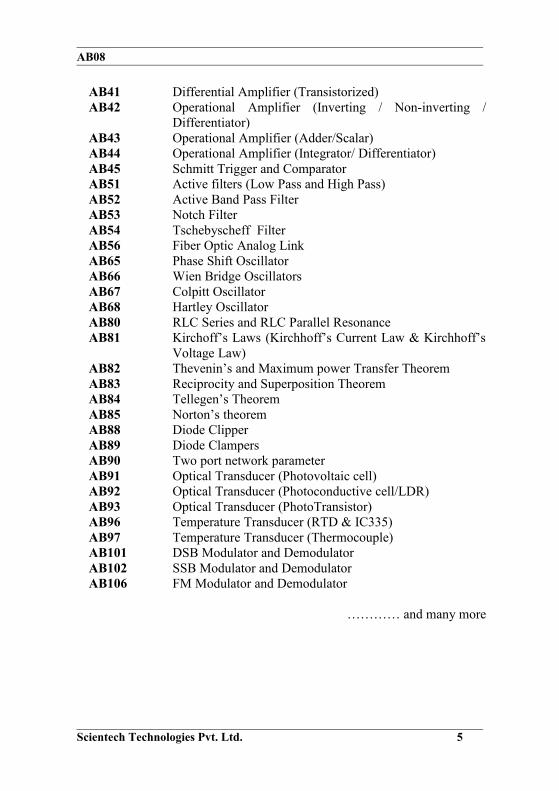
AB01 Diode characteristics (Si, Zener, LED)AB02 Transistor characteristics (CB NPN)AB03 Transistor characteristics (CB PNP)AB04 Transistor characteristics (CE NPN)AB05 Transistor characteristics (CE PNP)AB06 Transistor characteristics (CC NPN)AB07 Transistor characteristics (CC PNP)AB09 Rectifier CircuitsAB10 Wheatstone BridgeAB11 Maxwell’s BridgeAB14 Darlington PairAB15 Common Emitter AmplifierAB16 Common Collector AmplifierAB17 Common Base AmplifierAB18 Cascode AmplifierAB19 RC-Coupled AmplifierAB20 Direct Coupled AmplifierAB21 Class a AmplifierAB22 Class B Amplifier (push pull emitter follower)AB23 Class C Tuned AmplifierAB25 Phase Locked Loop (FM Demodulator & Frequency
Divider / Multiplier)AB28 Multivibrator (Mono stable / Astable)AB29 F-V and V-F ConverterAB30 V-I and I-V ConverterAB31 Zener Voltage Regulator AB32 Transistor Series Voltage RegulatorAB33 Transistor Shunt Voltage Regulator
Scientech Technologies Pvt. Ltd. 4
AB08
AB41 Differential Amplifier (Transistorized)AB42 Operational Amplifier (Inverting / Non-inverting /
Differentiator)AB43 Operational Amplifier (Adder/Scalar)AB44 Operational Amplifier (Integrator/ Differentiator)AB45 Schmitt Trigger and ComparatorAB51 Active filters (Low Pass and High Pass)AB52 Active Band Pass Filter AB53 Notch Filter AB54 Tschebyscheff FilterAB56 Fiber Optic Analog LinkAB65 Phase Shift OscillatorAB66 Wien Bridge OscillatorsAB67 Colpitt OscillatorAB68 Hartley OscillatorAB80 RLC Series and RLC Parallel Resonance AB81 Kirchoff’s Laws (Kirchhoff’s Current Law & Kirchhoff’s
Voltage Law)AB82 Thevenin’s and Maximum power Transfer TheoremAB83 Reciprocity and Superposition TheoremAB84 Tellegen’s TheoremAB85 Norton’s theoremAB88 Diode ClipperAB89 Diode ClampersAB90 Two port network parameterAB91 Optical Transducer (Photovoltaic cell)AB92 Optical Transducer (Photoconductive cell/LDR)AB93 Optical Transducer (PhotoTransistor)AB96 Temperature Transducer (RTD & IC335)AB97 Temperature Transducer (Thermocouple)AB101 DSB Modulator and DemodulatorAB102 SSB Modulator and DemodulatorAB106 FM Modulator and Demodulator
………… and many more
Scientech Technologies Pvt. Ltd. 5

AB08
THEORY
FET is a voltage controlled current device so its characteristics are the curves which represent relationship between different dc currents and voltages. These are helpful in studying different region of operation of a Field effect transistor when connected in a circuit. The two important characteristics of a Field Effect Transistor are:
1. Output /Drain characteristic.
2. Transfer characteristic.
Output / Drain Characteristics :
It is the curve plotted between output drain current ID verses output drain to source voltage VDS for constant values of input Gate to source voltage VGS
as shown in Fig 1.
Fig. 1It can be subdivided into following four regions:
Scientech Technologies Pvt. Ltd. 6

AB08
Ohmic region OA :
This part of the characteristic is linear indicating that for low values of VDS, current varies directly with voltage following Ohm's Law. It means that JFET behaves like an ordinary resistor till point A (called knee) is reached.
Curve AB :
In this region, ID increases at inverse square law rate upto point B which is called Pinch-off point. This progressive fall in the rate of increase of ID is caused by the square law increase in the depletion region at each gate up to point B where the two regions are closest without touching each other. The drain to source voltage VDS corresponding to point B is called pinch-off voltage VPO.
Pinch-off region BC :
It is also known as saturation region or 'amplifier' region. Here, JFET operates as a constant-current device because ID is relatively independent of VDS. It is due to the fact that as VDS increases channel resistance also increases proportionally thereby keeping ID practically constant at IDSS.Drain current in this region is given by Shockley's equation
It is the normal operating region of the JFET when used as an amplifier.
ID = IDSS [1 – (VGS / VPO)2 ] = IDSS [ – (VGS / VGS (off))2 ]
Breakdown region :
If VDS is increased beyond its value corresponding to point C (called avalanche breakdown voltage), JFET enters the breakdown region where ID
increases to an extensive value. This happens because the reversed biased gate channel PN junction undergoes avalanche breakdown when small change in VDS produce very large change in ID.
JFET characteristics with External Bias :
Fig 2 shows a family of ID verses VDS curves for different values of VGS. It is seen that as the negative gate bias voltage is increased:Pinch-off voltage VP is reached at a lower value of VDS than VGS = 0. Value of VDS for breakdown is decreased.
Scientech Technologies Pvt. Ltd. 7

AB08
Fig. 2
Transfer Characteristic :
It is the curve plotted between output drain current versus input Gate to source voltage for constant values of output drain to source voltage as shown in Fig 3.
Fig. 3
Scientech Technologies Pvt. Ltd. 8

AB08
It is similar to the transconductance characteristics of a vacuum tube or a transistor. It is shows that when VGS = 0, ID = IDSS and when ID = 0, VGS = VPO. The transfer characteristic approximately follows the equation
ID = IDSS [ 1 − (VGS / VPO)2 ] = IDSS [ 1 − (VGS / VGS(off))2 ]
The above equation can be written as VGS = VGS(off) [ 1 − (ID / IDSS)1/2 ] These characteristics can also be obtained from the drain/output characteristics by reading off VGS and IDSS values for different values of VDS.
The various parameters of a JFET can be obtained from its two characteristics.
The main parameters of a JFET when connected in common source mode are
1. AC Drain Resistance, rd :
It is the ac resistance between drain and source terminals when JFET is operating in the pinch-off region. It is given by
rd = change in VDS at VGS constant or rd = VDS / ID | VGS
change in ID
An alternative name is dynamic drain resistance. It is given by the slope of the drain characteristics in the pinch off region. It is sometimes written as rds
emphasizing the fact that it is the resistance from drain to source. Since rd is usually the output resistance of a JFET, it may also be expressed as an output admittance yos. Obviously, yos = 1/rd. It has a very high value.
2. Transconductance, gm :
It is simply the slope of transfer characteristics
gm = change in ID at VDS constant or rd = ID / VGS | VDS
change in VGS
Its unit is siemens (S) /mho. It is also called forward transconductance (gfs) or forward transadmittance Yfs. The transconductance measured at IDSS is written as gmo.
Mathematically
gm = gmo [1− (VGS / VP)]
Scientech Technologies Pvt. Ltd. 9

AB08
3. Amplification factor, µ :
It is given by
µ = change in VDS at ID constant or µ = VDS / VGS | IDS
change in VGS
It can be proved from above that µ = gm * rd = gfs * rd
4. DC drain resistance, RDS :
It is also called the static or ohmic resistance of the channel. It is given by
RDS = VDS / ID
Scientech Technologies Pvt. Ltd. 10

AB08
EXPERIMENT
Objective :
To study the characteristics of JFET (Junction field effect transistor) in common source configuration and to evaluate:
1. AC drain resistance
2. Transconductance
3. Amplification factor
4. Drain Resistance
Apparatus required :
1. Analog board of AB08.
2. DC power supplies +12V, -5V from external source or ST2612 Analog Lab.
3. Digital Multimeter (3 numbers).
4. 2 mm patch cords.
Circuit diagram :
Circuit used to plot different characteristics of transistor is shown in Fig 4.
Scientech Technologies Pvt. Ltd. 11

AB08
Fig. 4Procedure :
• Connect -5V and + 12V dc power supplies at there indicated position from external source or ST2612 Analog Lab.
• To plot Drain characteristics proceed as follows:
1. Rotate both the potentiometer P1 and P2 fully in CCW (counter clockwise direction).
2. Connect Ammeter between test point 3 and 4 to measure output drain current ID(mA).
3. Connect one voltmeter between test point 1 and ground to measure input voltage VGS other voltmeter between test point 2 and ground to measure output voltage VDS.
4. Switch ON the power supply.
5. Vary the potentiometer P2 so as to increase the value of output voltage VDS from zero to 10V in step and measure the corresponding values of output drain current ID for different constant value of output voltage VDS in an observation table 1.
Scientech Technologies Pvt. Ltd. 12

AB08
6. Rotate potentiometer P2 fully in CCW direction.
7. Rotate potentiometer P1 and set the value of input gate to source voltage at some constant value (-1V, -2V, -3V……….)
8. Repeat the procedure from step 6 for different sets of input voltage VGS.
9. Plot a curve between output voltage VDS and output current ID at different constant values of input gate to source voltage as shown in Fig 2 using suitable scale with the help of observation table 1. This curve is the required output/Drain characteristic.
Observation Table 1 :
S.no.Output voltage
VDS (volt)
Output Drain current ID (mA) at constant Value of input voltage
VGS = 0V VGS = -1V VGS = -2V VGS = -3V
1. 0.0V
2. 1.0V
3. 2.0V
4. 3.0V
5. 4.0V
6. 5.0V
7. 6.0V
8. 7.0V
9. 8.0V
10. 9.0V
• To plot Transfer characteristics proceed as follows:
1. Switch OFF the power supply.
2. Rotate both the potentiometer P1 and P2 fully in CCW (counter clockwise direction).
Scientech Technologies Pvt. Ltd. 13

AB08
3. Connect voltmeter between test point 6 and ground to measure output voltage VDS.
4. Connect one Ammeter between test point 3 and 4 to measure output current ID(mA)
5. Vary potentiometer P2 and set a value of output voltage VDS at some constant value (1 V, 2V, 3V..........)
6. Vary the potentiometer P1 so as to increase the value of input voltage VGS from zero to maximum value in step and measure the corresponding values of output current ID in an observation table 2
7. Rotate potentiometer P1 fully in CCW direction.
8. Repeat the procedure from step 5 for different sets of output voltage VDS.
9. Plot a curve between input voltage VGS and output current ID as shown in Fig 3 using suitable scale with the help of observation table 2. This curve is the required Transfer characteristic.
Observation Table 2 :
S.no.
Inputvoltage
VGS
(volt)
Output Drain current ID (mA) at constant value of input voltage
VDS = 1V VDS = 2V VDS = 3V VDS = 4V VDS = 5V
1. 0.0V
2. -0.5V
3. -1.0V
4. -1.5V
5. -2.0V
6. -2.5V
7. -3.0V
8. -3.5V
9. -4.0V
Scientech Technologies Pvt. Ltd. 14

AB08
Scientech Technologies Pvt. Ltd. 15

AB08
Calculations :
1. AC Drain Resistance, rd :
It is the ac resistance between drain and source terminals when JFET is operating in the pinch-off region. To calculate AC drain resistance calculate the slope of the drain characteristics in the pinch off region obtained from observation Table 1.
rd = change in VDS at VGS constant or rd = VDS / ID | VGS
change in ID
It has a very high value.
2. Transconductance, gm :
To calculate transconductance determine slope of the transfer characteristics obtained from Observation Table 2
gm = change in ID at VDS constant or rd = ID / VGS | VDS
change in VGS
Its unit is siemens (S) / mho.
3. Amplification factor, µ :
It is given by
µ = change in VDS at ID constant or µ = VDS / VGS | IDS
change in VGS
or µ = gm * rd
4. DC drain resistance, RDS :
It is also called the static or ohmic resistance of the channel. It is given by
RDS = VDS /ID
Results :
AC
Drain Resistance rd = _____________
Transconductance, gm = _____________
Amplification factor µ = _____________
Scientech Technologies Pvt. Ltd. 16

AB08
DC drain resistance, RDS = _____________
Scientech Technologies Pvt. Ltd. 17

AB08
DATASHEET
Scientech Technologies Pvt. Ltd. 18

AB08
Scientech Technologies Pvt. Ltd. 19

AB08
WARRANTY
1) We guarantee the instrument against all manufacturing defects during 24 months from the date of sale by us or through our dealers.
2) The guarantee covers manufacturing defects in respect of indigenous components and material limited to the warranty extended to us by the original manufacturer, and defect will be rectified as far as lies within our control.
3) The guarantee will become INVALID.a) If the instrument is not operated as per instruction given in the
instruction manual. b) If the agreed payment terms and other conditions of sale are not
followed.c) If the customer resells the instrument to another party.d) Provided no attempt have been made to service and modify the
instrument.4) The non-working of the instrument is to be communicated to us
immediately giving full details of the complaints and defects noticed specifically mentioning the type and sr. no. of the instrument, date of purchase etc.
5) The repair work will be carried out, provided the instrument is dispatched securely packed and insured with the railways. To and fro charges will be to the account of the customer.
DESPATCH PROCEDURE FOR SERVICE
Should it become necessary to send back the instrument to factory please observe the following procedure:
1) Before dispatching the instrument please write to us giving fully details of the fault noticed.
2) After receipt of your letter our repairs dept. will advise you whether it is necessary to send the instrument back to us for repairs or the adjustment is possible in your premises.
Dispatch the instrument (only on the receipt of our advice) securely packed in original packing duly insured and freight paid along with accessories and a copy of the details noticed to us at our factory address.
Scientech Technologies Pvt. Ltd. 20

AB08
LIST OF SERVICE CENTERS
1. Scientech Technologies Pvt. Ltd.90, Electronic Complex Ph : (0731) 2570301Pardesipura, Email : [email protected] INDORE – 452010
2. Scientech Technologies Pvt. Ltd.First Floor, C-19, Ph : (011) 22157370, 22157371F.I.E., Patparganj Industrial Area, Fax : (011) 22157369DELHI – 110092 Email : [email protected]
3. Scientech Technologies Pvt. Ltd.New no.2, Old no.10, 4th street Ph : (044) 42187548, 42187549
Venkateswara nagar, Adyar Fax : (044) 42187549CHENNAI – 600025 Email : [email protected]
4. Scientech Technologies Pvt. Ltd. 202/19, 4th main street Ph : (080) 51285011 Ganganagar, Fax : (080) 51285022 BANGALORE- 560032 Email : [email protected]. Scientech Technologies Pvt. Ltd.
8,1st floor, 123-Hariram Mansion, Ph : (022) 56299457 Dada Saheb Phalke road, Fax : (022) 24168767 Dadar (East), Email : [email protected] MUMBAI –400014 6. Scientech Technologies Pvt. Ltd. 988, Sadashiv Peth, Ph : (020) 24461673 Gyan Prabodhini Lane, Fax : (020) 24482403 PUNE – 411030 Email : [email protected]. Scientech Technologies Pvt. Ltd SPS Apartment, 1st Floor Ph : +913355266800 2, Ahmed Mamoji Street, Email : [email protected]
Behind Jaiswal Hospital, Liluah, HOWRAH-711204 W.B.8. Scientech Technologies Pvt. Ltd Flat No. 205, 2nd Floor, Ph : (040) 55465643 Lakshminarayana Apartments Email : [email protected] ‘C’ wing, Street No. 17, Himaytnagar, HYDERABAD- 500029
Scientech Technologies Pvt. Ltd. 21

AB08
LIST OF ACCESSORIES
1. 2mm Patch cord (red) .........................................................2 Nos.
2. 2mm Patch cord (black) ......................................................2 Nos.
3. 2mm Patch cord (blue) ........................................................1 Nos.
Scientech Technologies Pvt. Ltd. 22