Aalborg Universitet Resource Minimal Architecture Design ...
165
Aalborg Universitet Resource Minimal Architecture Design for Software Defined Radio Front-Ends Awan, Mehmood-Ur-Rehman Publication date: 2013 Document Version Accepted author manuscript, peer reviewed version Link to publication from Aalborg University Citation for published version (APA): Awan, M-U-R. (2013). Resource Minimal Architecture Design for Software Defined Radio Front-Ends. General rights Copyright and moral rights for the publications made accessible in the public portal are retained by the authors and/or other copyright owners and it is a condition of accessing publications that users recognise and abide by the legal requirements associated with these rights. ? Users may download and print one copy of any publication from the public portal for the purpose of private study or research. ? You may not further distribute the material or use it for any profit-making activity or commercial gain ? You may freely distribute the URL identifying the publication in the public portal ? Take down policy If you believe that this document breaches copyright please contact us at [email protected] providing details, and we will remove access to the work immediately and investigate your claim. Downloaded from vbn.aau.dk on: December 06, 2021
Transcript of Aalborg Universitet Resource Minimal Architecture Design ...

Aalborg Universitet
Resource Minimal Architecture Design for Software Defined Radio Front-Ends
Awan, Mehmood-Ur-Rehman
Publication date:2013
Document VersionAccepted author manuscript, peer reviewed version
Link to publication from Aalborg University
Citation for published version (APA):Awan, M-U-R. (2013). Resource Minimal Architecture Design for Software Defined Radio Front-Ends.
General rightsCopyright and moral rights for the publications made accessible in the public portal are retained by the authors and/or other copyright ownersand it is a condition of accessing publications that users recognise and abide by the legal requirements associated with these rights.
? Users may download and print one copy of any publication from the public portal for the purpose of private study or research. ? You may not further distribute the material or use it for any profit-making activity or commercial gain ? You may freely distribute the URL identifying the publication in the public portal ?
Take down policyIf you believe that this document breaches copyright please contact us at [email protected] providing details, and we will remove access tothe work immediately and investigate your claim.
Downloaded from vbn.aau.dk on: December 06, 2021

Resource Minimal Architecture Designfor
Software Defined Radio Front-Ends
PhD Dissertation
Mehmood Ur Rehman Awan

Resource Minimal Architecture Design for Software Defined Radio Front-Ends
PhD Dissertation
This dissertation is a revised version of the dissertation”Resource Optimal Architecture Design for Software DefinedRadio Front-Ends”submitted to Faculty of Engineering, Science and Medicine at Aalborg University,and defended successfully on March 22, 2013.
ISBN: 978-87-7152-002-6March 2013
Copyright 2013c©Mehmood Ur Rehman Awan (except where stated otherwise)Technology Platforms Section,Department of Electronic Systems, Aalborg UniversityNiels Jernes Vej 129220 Aalborg Øst

Resource Minimal Architecture Design for Software Defined RadioFront-Ends
PhD Dissertation by:Mehmood Ur Rehman Awan
Supervised by:
Peter KochAssociate ProfessorTechnology Platforms Section, Dept. of Electronic Systems,Aalborg University, Denmark
fredric j. harris (co-supervisor)ProfessorDept. of Electrical & Computer Engineering,San Diego State University, CA, USA
List of Publications
• Mehmood Awan, Yannick Le Moullec, Peter Koch, and fred harris, ”PolyphaseFilter Banks for Embedded Sample Rate Changes in Digital Radio Front-Ends”,Special Issue on advances in Digital Front-End and SoftwareRF Processing: PartII, ZTE Communications, Vol. 9, No. 4, pp. 3-9, Dec 2011. ISSN 1673-5188.
• Mehmood Awan, Yannick Le Moullec, Peter Koch, and fred harris, ”Hardware Ar-chitecture Analysis of Polyphase Filter Banks Performing Embedded Resamplingfor Software Defined Radio Front-Ends”,100G and Beyond: Trends in Ultrahigh-Speed Communications (Part I), ZTE Communications, Vol. 10, No. 1, pp. 54-62,Mar 2012. ISSN 1673-5188
• Mehmood Awan, fred harris, and Peter Koch, ”Time and Power Optimizations inFPGA-Based Architectures for Polyphase Channelizers”,45th Asilomar Confer-ence on Signals, Systems, and Computers, Pacific Grove, California, Nov. 6-9,2011, pp. 914-918. ISBN: 978-1-4673-0323-1
• Mehmood Awan, Peter Koch, Chris Dick, and fred harris, ”FPGAImplementationAnalysis of Polyphase Channelizer Performing Sample Rate Change Required forboth Matched Filtering and Channel Frequency Spacing”,44th Asilomar Confer-ence on Signals, Systems, and Computers, Pacific Grove, California, Nov. 7-10,2010, pp. 414-418. ISBN: 978-1-4244-9721-8
• Mehmood Awan, and Peter Koch, ”Combined Matched Filter and Arbitrary Inter-polator for Symbol Timing Synchronization in SDR Receivers”, 13th IEEE Sympo-sium on Design and Diagnostics of Electronic Circuits and Systems, Vienna Aus-tria, April 14-16, 2010, pp. 153-156. ISBN (print): 978-1-4244-6610-8/10
III

• Mehmood Awan, and Peter Koch, ”Polyphase Channelizer as Bandpass Filters inMulti-Standard Software Defined Radios”,2nd International Workshop on Cogni-tive Radio and Advanced Spectrum Management (CogART 2009), Aalborg, May18-20, 2009, pp. 59-63. ISBN: 978-1-4244-4066-5
This thesis has been submitted to the Faculty of Engineeringand Science at AalborgUniversity for assessment in partial fulfillment of the PhD degree. The thesis is based onthe published scientific papers which are listed above. Parts of the papers are used directlyor indirectly in the extended summary of the thesis. As part of the assessment, co-authorstatements have been made available to the assessment committee and are also availableat the Faculty. The thesis is not in its present form acceptable for open publication butonly in limited and closed circulation as copyright may not be ensured.
IV
Preface
The work was conducted from October 2008 to November 2012 under the research activ-ities by Center for Software Defined Radio at Aalborg University.
Acknowledgements
I would like to thank my supervisor Assoc. Prof. Peter Koch and honorary co-supervisorProf. fredric j. harris for their inspiration, contributions, and support during the wholeprocess of the PhD work. I also thank Assoc. Prof. Yannick Le Moullec for his valuablecontributions. I also thank Prof. fredric j. harris for inviting me to San Diego State Uni-versity (SDSU) for my external research stay from February 2010 to July 2010. It wasa wonderful time and experience, where I learned and explored the power of the multi-rate signal processing especially for Software Defined Radio. A special thanks goes toMichael Bayliss for his cooperation and hospitality duringmy stay in San Diego, CA. Ithank Chris Dick from Xilinx Inc. for his cooperation. Furthermore, I would like to thankmy colleagues at Aalborg University, Alex Aaen Birklykke, Muhammad Mahtab Alam,Rasmus Abildgren, Andreas Popp, and Jesper Michael Kristensen and my colleagues atSDSU, Elettra Venosa, and Xiaofei Chen for making every workday an enjoyable time.The same goes for the rest of my colleagues in the Technology Platforms Section.
Last but not least I thank my family and friends for their encouragement, company, andsupport that has always given me the energy and motivation towork.
Aalborg, Denmark, November 2012 Mehmood Ur Rehman Awan
V


List of Abbreviations
The following abbreviations are used throughout the thesis:
ADC Analog-to-Digital Converter
AGC Automatic Gain Control
AM Amplitude Modulation
ASIC Application Specific Integrated Circuit
CIC Cascade Integrator Comb
CLB Configurable Logic Block
CMOS Complementary Metal-Oxide-Semiconductor
CORDIC COordinate Rotation DIgital Computer
CR Cognitive Radio
DAC Digital-to-Analog Converter
DCM Digital Clock Manager
DDC Digital Down Converter
DDS Direct Digital Synthesis
DFE Digital Front-End
DFT Discrete Fourier Transform
DFTFB Discrete Fourier Transform Filter Bank
DSE Design Space Exploration
DSP Digital Signal Processing
DUC Digital Up Converter
FFT Fast Fourier Transform
FIFO First-In-First-Out
FIR Finite Impulse Response
FM Frequency Modulation
FPGA Field-Programmable Gate Array
GUI Graphical User Interface
HDTV High Definition Television
VII

HW Hardware
IC Integrated Circuit
IF Intermediate Frequency
IFFT Inverse Fast Fourier Transform
IIR Infinite Impulse Response
IP Intellectual Property
ISE (Xilinx) Integrated System Environment
LPA Load Process Architecture
LUT Look-Up Table
MAC Multiply-and-ACcumulate
MPRB Modulated Perfect Reconstruction Bank
OQAM Offset Quadrature Amplitude Modulation
PC Personal Computer
PR Perfect Reconstruction
QMF Quadrature Mirror Filter
RA Runtime Architecture
SDR Software Defined Radio
SNR Signal-to-Noise Ratio
SRC Sample Rate Conversion
SW Software
TRF Tuned Radio Frequency
VCO Voltage Controlled Oscillator
VHDL Very-High-Speed-Integrated-Circuit (VHSIC) Hardware Description Language
VLSI Very Large Scale Integration
VIII

Contents
Contents IX
Abstract XI
Dansk Resume XIII
1 Introduction 11.1 History of Radio Transceivers . . . . . . . . . . . . . . . . . . . . . .. 11.2 Software Defined Radio . . . . . . . . . . . . . . . . . . . . . . . . . . . 31.3 Multirate Signal Processing . . . . . . . . . . . . . . . . . . . . . . .. . 71.4 Channelization . . . . . . . . . . . . . . . . . . . . . . . . . . . . . . . 91.5 Synchronization . . . . . . . . . . . . . . . . . . . . . . . . . . . . . . . 151.6 Modern Receivers - state-of-the-art . . . . . . . . . . . . . . . .. . . . . 171.7 Polyphase Filter Bank Mapping - State-of-the-Art . . . . .. . . . . . . . 201.8 Thesis formulation . . . . . . . . . . . . . . . . . . . . . . . . . . . . . 211.9 Outline of the Dissertation . . . . . . . . . . . . . . . . . . . . . . . .. 22
2 Design Space Exploration of Polyphase Filter Banks for High PerformanceSDR Front-Ends 232.1 Polyphase Filter Structures . . . . . . . . . . . . . . . . . . . . . . .. . 232.2 Comparative Analysis . . . . . . . . . . . . . . . . . . . . . . . . . . . . 252.3 Subfilter Architectures . . . . . . . . . . . . . . . . . . . . . . . . . . .262.4 Non-Maximally Decimated Systems . . . . . . . . . . . . . . . . . . .. 272.5 Optimizations for Area Resources . . . . . . . . . . . . . . . . . . .. . 282.6 Architecture Exploration . . . . . . . . . . . . . . . . . . . . . . . . .. 312.7 Optimization for Enhanced Clock Speed Performance . . . .. . . . . . . 342.8 Explored Solution Space . . . . . . . . . . . . . . . . . . . . . . . . . . 35
3 Summary of Contributions 45
4 Conclusion 51
5 List of Publications 59
References 61
IX

CONTENTS
Contributions 69
Paper A: Polyphase Filter Banks for Embedded Sample Rate Changes in Dig-ital Radio Front-Ends 71
Paper B: Hardware Architecture Analysis of Polyphase Filter Banks Perform-ing Embedded Resampling for Software Defined Radio Front-Ends 85
Paper C: Time and Power Optimizations in FPGA-Based Architectures forPolyphase Channelizers 105
Paper D: FPGA Implementation Analysis of Polyphase Channelizer Perform-ing Sample Rate Change Required for both Matched Filtering and Chan-nel Frequency Spacing 117
Paper E: Combined Matched Filter and Arbitrary Interpolato r for SymbolTiming Synchronization in SDR Receivers 129
Paper F: Polyphase Channelizer as Bandpass Filters in Multi-Standard Soft-ware Defined Radios 139
X

Abstract
The high and constantly increasing demand to develop radio transceivers with enhancedfunctionalities, inter-standard portability, higher throughputs, compact physical size, lowcost, and longer battery lifetime impose challenges on the radio designer. A SoftwareDefined Radio is capable of meeting these challenges provided (i) enhanced signal pro-cessing algorithms with reduced complexities, (ii) high performance HW/SW platforms,and (iii) the optimized architectural design that finally maps the algorithms to the pro-cessing platform.This dissertation focuses on a resource minimal architecture design for Software DefinedRadio (SDR) front-ends targeting a reconfigurable architecture platform using a FieldProgrammable Gate Array (FPGA). Front-end design techniques ranging from legacy ra-dios to the state-of-the-art radios are presented and analyzed. The results showed thatmultirate signal processing based techniques provide highperformance solutions at a re-duced resource complexity, thus making them highly suitable for the SDR front-ends.The outcome is a set of structural guidelines for the designer which can be used to ob-tain an Area, Time, operating clock Speed, and Power minimized architectural design forSDR front-ends using polyphase filter bank solutions - a multirate signal processing tech-nique. The design space of reconfigurable architectures is explored to suggest differentmapping solutions for polyphase filter bank which are analyzed based on their resourceusage and corresponding performances. Non-maximally decimated operating scenariosare identified and scheduling schemes are proposed to meet their output time constraints.The scheduling schemes applied are: Load-Process scheduler, Interlaced Load-Processscheduler, and Runtime scheduler. The proposed architectures are based on these sched-ulers, which in the light of exploration of the reconfigurable target space (Xilinx Virtex-5FPGA) are presented to compare resource and performance metrics.The dissertation is composed of four parts: First, the related design challenges and state-of-the-art in SDR front-ends are discussed. The focus is on design solutions with the leastcomputational requirements while operating at the lowest possible clock rate, and havingthe ability to embed several functions together. Second, a design space exploration ofpolyphase filter banks is presented and a set of structural design guidelines are suggestedto the designer enabling Area, Time, operating clock Speed,and Power optimized solu-tions for SDR front-end designs. Third, a summary of the contributions is provided whichrelates to the published papers. Finally, a conclusion and outlook are given.The main body of the dissertation is composed of six peer-reviewed papers which presentthe scientific contributions. The results show that the polyphase filter (bank) can embedmultiple functions in its operation in a cost effective manner, such as combined arbitraryresampling, match filtering and symbol timing recovery, andrational resampling apartfrom a maximally decimated scenario. Furthermore, the suggested Runtime Architecture(RA) based on a Runtime scheduling scheme, with (i) distributed RAM organized as apipelined register bank, (ii) distributed RAM or pipelinedblock RAM based coefficientbank, and (iii) systolic array of DSP48E (dedicated computational resources on Xilinx
XI

CONTENTS
FPGA) slices based Multiply-Accumulate (MAC) is a preferred choice to enhanced per-formance and reduce latency for SDR digital front-ends.The lessons learned during the exploration of the solution space for the polyphase fil-ter banks provide a sound basis for the system designer to choose the solution(s) whichmeet(s) the normally tight resource and performance constraints. Besides, the formulateddesign guidelines which constitute our most important scientific contribution, can help thedesigner at any point in the design process, thus potentially leading to a reduced overallcost and time-to-market overhead.
XII

Dansk Resume
De til stadighed voksende krav, der stilles ifm. udvikling af radio-sendere og -modtageremed avancerede funktioner som eksempelvis understøttelseaf flere forskellige kommuni-kationsstandard, høje datatransmissions-rater, kompaktfysisk størrelse, lav pris og langbatterilevetid, medfører markante faglige udfordringer for den moderne radio-ingeniør.Med udbredelsen af den sakaldte ”software defined radio” (SDR), er der imidlertid tilve-jebragt et koncept, som er i stand til at imødekomme mange af nutidens krav og udfor-dringer, idet netop dette koncept gør brug af (i) højtydendesignalbehandlings-algoritmermed lav beregningsmæssig kompleksitet, (ii) avancerede HW/SW platforme, og ligeledes(iii) understøttes muligheden for at designe HW/SW-arkitekturer, som er skræddersyedetil de nødvendige signalbehandlings-algoritmer.Denne phd-afhandling fokuserer pa design af resource-minimale FPGA-baserede arkitek-turer til SDR modtageres front-ends, dvs. de første signalbehandlingsalgoritmer umiddel-bart efter analog-til-digital konverteringen. Vi præsenterer og analyserer design-teknikkerfor savel traditionelle som moderne radio front-ends, og vi viser at signalbehandlingsal-goritmer baseret pa det sakaldte ”multi-rate” princip med fordel kan benyttes til at frem-bringe højtydende SDR front-ends med reduceret ressource-forbrug. Vi tilvejebringerretningslinier for struktureret design med henblik pa at opna bedst mulig performancemht. fysisk areal, eksekveringstid, og effektforbrug for SDR front-end arkitekturer. Her-til udnytter vi sakaldte poly-fase filter-banker. Med udgangspunkt i omkonfigurerbareHW-arkitekturer afsøger vi det sakaldte design-løsningsrum med henblik pa at frem-sætte forslag til design-løsninger for poly-fase filter-banker. Løsningsforslagene evalueresift. det aktuelle ressource-forbrug og den givne performance. Vi identificerer scenarierbaseret pa ”non-maximal decimation” og vi foreslar i relation hertil eksekverings-planer,der imødekommer algoritmernes tidsmæssige krav. Planerneomfatter Load-Process, In-terlaced Load-Process og Runtime afvikling. Med udgangspunktheri foreslar vi tilhørendeHW-arkitekturer, hvis ressource-forbrug og performance analyseres.Afhandlingen bestar af fire hovedelementer; For det førsteforkuserer vi pa de udfor-dringer der er ved design af moderne SDR front-ends. Vores fokus er rettet mod design-løsninger med mindst mulig beregnings-kompleksitet, som kan udføres med den lavestmulige clock-frekvens, og som samtidig understøtter muligheden for at udføre adskil-lige funktioner i den samme operation. For det andet udforsker vi løsningsrummet forpoly-fase filterbanker med henblik pa at definere retningslinier for ressource-optimal de-sign af SDR front-ends. For det tredje gennemgar vi de resultater der er tilvejebragtog efterfølgende afrapporteret i form af videnskabelige artikler. Endelig konkluderer vivores arbejde og funderer over mulige fremtidige aktiviteter. De fundamentale resultater,som er publiceret i seks bedømte artikler, viser, at poly-fase filter-banker kan bringes tilat udføre flere samtidige funktioner, som eksempelvis ”arbitrary resampling”, ”matchedfiltering”, ”symbol timing recovery”, og ”rational resampling” (med undtagelse af mak-simal decimering scenariet). Desuden viser vores resultater, at den foretrukne løsning(dvs. bedst performance og korteste delay) er vores RuntimeArchitecture (RA), som
XIII
CONTENTS
baseres pa Runtime eksekverings-planlægning. Denne løsning kan realiseres ved brug afforskellige metoder til lagring af og multiplikation med filterkoefficienterne, eksempelvis(i) distribueret RAM organiseret som en pipelined register-bank, (ii) blok-RAM, eller (iii)et systolsk array bestaende af DSP48E beregningskerner (Xilinx FPGA).De opnaede resultater ifm. afsøgning af løsningsrummet for poly-fase filter-banken hartilvejebragt et solidt og nyskabende videngrundlag, som system-designeren kan benytteifm. valg og design af SDR front-end løsninger, der imødekommer strenge ressource-og performancemæssige krav. Den frembragte viden er omsat til strukturerede retningsli-nier for SDR front-end design, hvilke saledes udgør det mest fundamentale resultat ivores arbejde. Dette resultat har medført, at der nu kan udvikles løsninger, som er merekonkurrencedygtige mht. pris og udviklingstid end tidligere tiders løsninger.
XIV
1 Introduction
Telecommunication has penetrated into our daily life so much that it is difficult to imaginea world without it. From a fundamental point of view, communication is the transmis-sion of information from one point to another. The radio frequency devices transmittingand receiving the information are called transceivers. Theconstantly increasing demandsupon these radio devices are more functionality, higher throughput, compact physical size,and longer battery lifetime, and of course low cost. This requires not only advancementsin signal processing algorithms but also advances in processing platforms and architec-tural implementation. In this chapter we will review the fundamental development ofradio technologies, discuss the state-of-the-art, and conclude by formulating a hypothesiswhich will serve as the overall inspiration for our work.
1.1 History of Radio Transceivers
The history of the radio started with the discovery of electromagnetic waves by Maxwellin 1887. The successive inventions by Hertz, Marconi, and many others concerning prop-agation of waves and wireless telegraphy gave birth to various wireless technologies [1].Marconi revealed the first practical radio system (apparently copying an earlier inventionof Nicola Tesla) in 1895 which led to transatlantic radio communication in 1901 [2]. Theinvention of the crystal detector, as well as Fleming’s valve and De Forest’s audion im-proved the sensitivity of the receiver. Edwin Armstrong invented the regenerative setsbased radio receivers in 1906, which made long distance reception a reality. The develop-ment of valves (tubes) as an amplifier and regenerative detector (using positive feedback)tremendously improved radio performance in terms of gain and selectivity. The FirstWorld War further drove the development of radio receiver technology. The developmentof tuned radio frequency receiver (TRF) technology in 1920s, basically a chain of individ-ually tuned amplifiers, represented a major improvement in radio performance. Furtherimprovements include direct conversion and autodyne receivers. Direct conversion useda local oscillator based mixer, producing an audible signalthat is further amplified. Thisrequires separate valves for oscillator and mixer. The autodyne receiver used the samevalve for both mixer and oscillator making it difficult to optimize both functions [3]. Theneed for a higher level of selectivity and sensitivity performances led to the developmentof the superheterodyne receiver. This is a receiver with an amplifier at a fixed intermediatefrequency, and a filter. The incoming signal is mixed with a variable frequency oscilla-tor (local oscillator) to obtain the down-conversion at a fixed lower frequency called an
1
Introduction
Intermediate frequency (IF). The signal is further passed through a lowpass filter to re-ject the unwanted (mixing) components, and then finally amplified [2]. This processingimproved the selectivity of the receiver, enhanced the gainfor valves being used at thelower frequencies (after the frequency conversion), and reduced the circuit oscillationproblems [3].
In the late 1940s the transistor (using semiconductor technology) was invented whichlater replaced the vacuum tubes in radio receivers during the 1950s and 1960s [3] [4] [5].These transistor devices turn out to be miniature, reliable, long lasting, and consume lesspower and generate less heat dissipation as compared to their counterpart, as vacuumtubes are fragile, bulky, unreliable, power hungry, and have high heat dissipation. Tran-sistor radios became attractive for their inherent features. The realization of complexelectronic circuits using a large number of transistors andtheir required interconnects ledto further developments in semiconductor technology leading to the Integrated Circuit(IC). This enabled radio receiver technology to utilize high performance circuits that canbe built at low cost, and in a significantly reduced volume. The technology developmentsresulted in new techniques, for example, a frequency synthesizer realizing a phase lockloop in the digital domain [4]. This synthesizer generates aprecise and stable local oscil-lator signal for the receiver. With the further advancements in receiver technology, manyof the functions performed in the analog domain have been replaced by digital methodsusing Digital Signal Processing (DSP) technology. The benefit is that the DSP techniquesare not affected by temperature and other physical variables, electronic noise, and aging.
DSP based radio transceivers have passed through several generations of architectures.The traditional heterodyne architecture, considered the first generation of digital radioarchitecture, is shown in Fig. 1.1(a). It consists of a dual-stage down-converter, and onlythe baseband processing is done in the digital domain [6]. Inthe first stage, the RF signalis down-converted to a bandlimited Intermediate Frequency(IF). In the second stage, theIF filter output is again down-converted to baseband by a matched-quadrature mixer, andmatched baseband filters that perform final bandwidth control. Next, the signal passesinto the digital domain where the output of the analog-to-digital converter (ADC) is pro-cessed by digital signal processing (DSP) engines. These engines perform the requiredbaseband processing, that is, synchronization, equalization, demodulation, detection, anddecoding. The problem with this type of architecture is thatgain and phase are imbalancedfor the in-phase and quadrature (I/Q) components. This results in cross-talk between thenarrowband channels due to aging (time, temperature) of theanalog components of thequadrature down-converter. Each imbalance-related spectral image must be lower thanthe desired spectral term, and this is difficult to sustain over time and at varying tempera-ture.
The need for extreme I/Q balance gave rise to the next generation of digital radios wherethe second stage (IF) down-conversion and, consequently, the channelization process isdigital, as shown in Fig. 1.1(b). Digital conversion at IF provides greater control over theimbalance by manipulating the number of bits involved in thearithmetic operation. Theprecision of the coefficients used in the filtering process sets an upper limit for spectralartifacts at−5 dB/bit. This means that 12-bit arithmetic can achieve image levels below−60 dB [6]. The DSP based complex down-conversion, however, has two advantages:
2

1.2 Software Defined Radio
��� ���
��������� ���
��
����
����
��
����
�������
��
� ! "�# ��
���
��������� ���
����
����
����
����
�� � ! "�# ��
Figure 1.1: (a) First generation of digital radio receiver architecture, and (b) Secondgeneration of digital radio receiver architecture.
(i) the spectral images are controlled so that they are belowthe quantization noise floorof the ADC involved in the conversion process, and (ii) the digital filters before and afterthe mixers are designed to have linear phase characteristics [6].
With more functions performed in DSP, the Personal Computer(PC) radio evolved. Thishas great advantage of being field upgradable both for existing and new functionalities.A Graphical User Interface (GUI) provides unlimited flexibility to the radio and newfeatures can be added simply by a software upgrade instead ofadding more hardwarecomponents. The next level in radio / software integration is Software Defined Radios(SDR).
1.2 Software Defined Radio
The concept of the SDR originates from the work of Mitola [7] in 1995, where a softwareadaptable radio architecture was proposed that enable the radio to automatically adjustto several different communication standards. This means that SDR is a radio communi-cation system which can tune to any frequency band and receive any modulation acrossa large frequency spectrum by means of programmable hardware which is controlled bysoftware. An Ideal Software Radio (ISR) is shown in Fig. 1.2.An SDR demodulating asimple AM broadcast may also be able to decode an HDTV broadcast simply by changingthe software for its programmable hardware. The SDR not onlyprovides high flexibilityto adapt the radio front-end for any desired modulation, channel bandwidth, or carrierfrequency, but also provides a cost effective solution by exploiting digital technology [8].
$%&'()*+(*,-)-+&'
.(%/01+01
203(%4-)51&6'0 7
81()1&99&6'0
:&1;<&10
,&+&
=(-30
>5'' ?(4+<&10 81()1&99&6-'-+@
Figure 1.2: An Ideal Software Defined Radio.
In the early years, SDR was mainly attractive for military applications where there is aneed for a single radio which can communicate with the many types of military radios that
3

Introduction
use different RF bands and different modulation schemes [9]. The emerging standards andthe high penetration of mobile communications systems strongly demand software radiobased mobile terminals and base stations for mobile communications systems [10] [11].There are lots of system level issues in the wireless communication industry which em-brace the essence and motivation for SDRs, such as;
• The rapid growth of commercial wireless network standards (2G, 2.5G, 3G, and4G) has caused incompatibility issues for subscribers, wireless network operators,and equipment vendors, due to differences in their link-layer protocol standards.
• Subscribers are obliged to buy new handsets to utilize new services.
• Wireless network operators have to migrate their network from one generation tothe next, while supporting both new and legacy handsets, andfurther they facedeployment issues while rolling-out new services.
• Handset vendors face challenges in manufacturing viable multi-mode handsets.
• Equipment vendors face challenges in developing newer generation equipment dueto short time-to-market requirements.
• The use of different air interface and link-layer protocolsacross various geogra-phies has restrained the deployment of global roaming facilities.
SDR technology promises to solve (at least to a certain extent) these problems by im-plementing the radio functionality as software modules running on a generic hardwareplatform. Further, multiple software modules implementing different standards can bepresent in the radio system. The software modules that implement new services/featurescan be downloaded over-the-air onto the handsets. This kindof flexibility offered by SDRsystems helps alleviate problems due to differing standards and issues related to deploy-ment of new services/features. There are a lot of advantagesof the full downloadable typeof software radio because the system can be changed on demandby changing the soft-ware. There are many advantages not only for operators and service providers, but alsofor government and commercial customers such as global roaming services, bug fixeswithout the need to recall the product, and new services can be added without changingthe terminals [12]. The most promising application of SDR isthe application of cognitiveradio (CR) [13]. As the radio spectrum becomes more and more sparse, making it a dif-ficult task to allocate new spectrum for new services. A CR is aware of its environment,internal state, its location, and can make a decision about its operating behaviour basedon this information.
Challenges
The idea behind SDR is to push as much radio functionality as possible into the digitaldomain via programmable digital hardware in order to achieve highly configurable de-signs [7]. This can be achieved by bringing the analog-to-digital conversion process (i.e.,Analog-to-Digital Converters (ADCs)) as close to the antenna as possible. An ISR, asshown in Fig. 1.2, samples the signal at RF, just after the antenna and is termed full-banddigitization. This straightforward approach is highly dependent on the ADC technology
4

1.2 Software Defined Radio
that could provide sufficient bandwidth and dynamic range performance for a SDR ap-plication together with low power consumption. The state-of-the-art ADC technology,however, bring the concept of Giga-Hertz sampling to a reality [14, 15].
In a realizable version of the software radio, shown in Fig. 1.3, the signal bandwidth mustbe reduced which is termed partial-band digitization. Thiscan be realized with conven-tional receiver techniques, i.e. a heterodyne receiver as described in the second generationof digital radio. The partial-band digitization demands ananalog front-end. Although itrequires less analog functionality as compared to the conventional analog receivers, therequirements are heavily increased due to the presence of higher bandwidth and the dy-namic range of the multi-channel signals for an SDR receiver. After digitization throughthe ADC, the signal of interest must be extracted from the digitized multi-channel signaland shifted to the baseband before the signal processing canbe performed. Furthermore,the sample rate applied to the selected signal must be in accordance with the air interface,which therefore requires some digital signal processing before the baseband processing.Traditionally, this digital signal processing is done through analog techniques in the ana-log front-end. The shifting of the ADC towards the antenna realized this functionality inthe digital domain. This is termed a Digital Front-End (DFE)which includes channeliza-tion (i.e., digital down conversion and channel filtering) and sample rate conversion [10].
������
����� �
���
� � ������
����� � ��
���
�����
������������� ������
!"��#!�$����!�
#%����� ���������
&�'(�� )��� #!�$����!�
*���+��, -�!.������
Figure 1.3: A realized version of Software Defined Radio.
The large bandwidth and high dynamic range of the signals to be processed by SDR even-tually result in high sample rate and large word lengths. Thehigh sample rates not onlyincrease power consumption but also make the DFE infeasiblefor implementation onprogrammable digital signal processor devices. Apart fromthe other critical and enablingcomponents of SDR (i.e., wideband analog front-end and the ADC) the requirement ofreconfigurability and/or programmability for SDR in the presence of very high samplerates turns the DFE into one of the most power- and time-critical functionalities of anSDR [16].
Architectures
The hardware platform is the most prominent and challengingcomponent of SDR asit has to provide massive computational power, flexibility,and at the same time meetstrict power- and size limitations [17] [18]. Therefore, the selection of hardware ar-chitectures for SDR based applications is not a trivial task. As SDR signal processingalgorithms are becoming more and more complex, the computational requirements onthe target HW/SW-platforms are becoming equally high, and consequently software so-lutions make it possible to establish a smooth transition from dedicated, single-purpose
5

Introduction
hardware (ASICs) to highly versatile general-purpose hardware systems such as FieldProgrammable Gate Array (FPGA).
In general, algorithmic complexity (sometimes referred toas Shannon’s law) is increas-ing at a rate faster than the processing capabilities of the hardware platforms (known asMoore’s law), which introduces a technology gap. Bridging this gap may be done bydeveloping new algorithms with reduced numerical complexity as well as devising alter-native hardware architectures with higher performance. The advances in silicon technol-ogy are progressing according to Moore’s law which however,cannot keep pace with thegrowing computational complexity. But at the same time Moore’s law has also led tothe fact that fabrication technologies now enable more transistors to be implemented on asingle die than typical state-of-the-art design tools can easily handle. This situation leadsto a so-called design-gap [19] [20]. According to the National Technology roadmap forsemiconductors, the number of transistors that could be fabricated on a die was increas-ing at a rate of about 60% a year, whereas the number of transistors that circuit designerscould design into new independent circuits was growing onlyby 20% a year [20]. Thistrend is observed in the DSP processor community where even the high-end DSP proces-sors do not push the transistor densities as described by Moore’s law [21].
To bring value to the state-of-the-art semiconductor products, the transistor budget mustbe used in a different way. That brings us to the FPGA technology which has improvedtremendously over the past five to ten years. An FPGA is the ultimate commercial devicefor architectural customization, providing a huge solution space to designers for con-structing their signal processing systems [21]. FPGAs are getting faster and their internalbuilding blocks are becoming more efficient in terms of clockspeed and reduced powerconsumption. The inherent parallel processing capabilityof FPGAs has made them thecore-processing engine in SDR applications. These devicesspend their transistor budgetin a fundamentally different way than ISA (Instruction Set Architecture) machines andhave enriched structure with CLBs (Configurable Logic Block), high speed I/Os, a va-riety of memory architectures, embedded hardware multipliers, Digital Clock Managers(DCMs), soft-core processors, and multi-gigabit transceivers (MGT). The most frequentlyused FPGA vendors are Xilinx [22] and Altera [23]. The internal architecture of a XilinxVirtex-5 FPGA is shown in Fig.1.4.
����� ���
��� ��
��� �����
������ � �������
���
�� � �������� !�� �" ����#�"&
��$�"��
%'()*+,-
./01
Figure 1.4: Architecture of Xilinx Virtex-5 FPGA.
FPGAs normally consist of two layers, where the first layer contains arrays of logicblocks, dedicated resources and routing between them. The actual configuration of the
6

1.3 Multirate Signal Processing
FPGA is determined by a second layer of memory, determining the functionality of thelogic and routing in the first layer.
The vast number of configurable parameters and customization in FPGA systems posesa great challenge to the designer as they offer a huge number of system, architectural,and logic design choices [24]. This creates a huge design space of possible architecturesand mappings which increases the time and effort needed for the final mapping (imple-mentation) of the system [25] [26] [27]. Finding the optimaldesign is often a matter oftrade-offs between costs and performance, thus opening a new era of designing highlyefficient FPGA based architectures requires design space exploration tools to help the de-signer to prune the design space.
The mapping process includes the design challenges of allocation, binding, and schedul-ing where allocation decides the number of resources (processing units) for performinga task, binding assigns the individual tasks to the processing units, and scheduling de-fines the relative task operations in time. Design space exploration is the evaluation ofpossible mapping solutions in the presence of a cost function, as expressed by Eq. 1.1,which may specify some of the parameters (e.g. execution time, area, power consump-tion, numerical precision etc.) as constrained by the requirements. A cost function canalso include other parameters such as price and developmenttime, degree of reconfigura-bility, maintainability, etc. It is generally accepted that finding an optimal design solutionfor a reconfigurable system is an NP complete [28] combinatorial optimization problem.We believe that a methodology/ tool can aid the designer during the design space explo-ration process in order to speed up the product development process and thereby meet thetime-to-market requirements. There exist many design methodologies, but there may stillbe room for further improvements. To our knowledge, very little has been done towardsexperimenting with the implementation of advanced DSP algorithms for SDR front-endson highly complex FPGA platforms. Therefore, in order to explore the possibilities andlimitations of such designs, we have decided to investigatethe advantages and disadvan-tages of design trade-off’s as compared to selected metricsin the cost function. The cost,C, of an implementation typically is expressed by a cost function,
C = f {A, T, P,N, ..} (1.1)
whereA is area or resource consumption,T is execution time,P is power consumption,andN is the numerical precision. Each parameter can be assigned aweighting factor thatdefines its significance, giving a cost function such asC = f {αA, βT, γP, ..}. Thus, a0.1 factor would mean that the corresponding parameter is 5 times less important than aparameter with a factor of 0.5. This is a somewhat abstract definition in the sense that theindividual parameters can not be really compared. These factors (or metrics) lead to thedesign constraints which need to be optimized, either individually or simultaneously. Inthis work, we will not consider the actual values of the weight factors.
1.3 Multirate Signal Processing
We have now explained the requirement for high computationally efficient and flexible ar-chitectures for SDR. But at the same time the design of high-performance SDR front-end
7

Introduction
requires advancements in the signal processing algorithmswith reduced computationaland/or resource complexities. Multirate signal processing specifies alternative ways ofperforming DSP tasks which are normally not available in traditional DSP designs. Itprovides not only a reduction in the cost, but also enhances the performance of the imple-mentation.
Multirate signal processing exploits sample rate changes at various stages of a system(hence the name multirate), in the form of decimation and interpolation of discrete timesequences [29]. From a traditional DSP perspective, the sample rate is selected to sat-isfy the Nyquist criterion. In multirate signal processing, selection and modificationof the sample rate are the primary considerations and options in the signal processingchain. This ability to change the sample rate within the processing stream introduces aremarkable list of processing tricks and performance enhancements. It enables the pro-cessing task to be performed at the lowest rate matching the signal bandwidth, which isthe Nyquist rate of the signal component of interest [30].
In contrast to a common processing task i.e., to reduce the bandwidth of a signal byfiltering and then reducing the sample rate to match the reduced bandwidth, a multiratesignal processing trick known as the Noble Identity interchanges the order of filtering andsample rate change so that the filter processing is done at thereduced output sample raterather than at the high input sample rate. The Noble Identityoperation is illustrated inFig. 1.5. The reduction in the sample rateprior to bandwidth reduction causes aliasing ofthe input spectrum. Multirate signal processing permits, and in fact, supports this inten-tional aliasing, which can be unwrapped by subsequent processing. Most of the tricks andenhancements associated with multirate signal processingare related to spectral aliasingdue to the sample rate change. The change in sample rate is also used to intentionallyalias a signal at one center frequency to another center frequency. This option includesaliasing a signal from an intermediate center frequency to baseband by reducing the sam-ple rate, as well as aliasing a signal from baseband to an intermediate center frequency byincreasing the sample rate [30].
����
������
�� ����
��� �
������
�� ��� ����
Figure 1.5: Noble Identity: A filter processing everyM th input sample followed by anM -to-1 down sampler is equivalent to an inputM -to-1 down-sampler followed by a filterprocessing every input sample.
Polyphase decomposition, which originated from the work byBellanger [31], plays afundamental role in many multirate DSP applications. Theseinclude efficient real-timeimplementation of decimation and interpolation filters, fractional sampling rate changingdevices, uniform DFT filter banks, and perfect reconstruction analysis/synthesis systems.A multirate polyphase filter can perform the tasks of a multichannel receiver which sig-nificantly reduces the amount of system resources required to perform multichannel pro-cessing and, consequently, reduces costs [6] [30]. Polyphase filter banks can be used in
8

1.4 Channelization
spectral sensing for cognitive radios [32]. Furthermore, they form a foundation of timingrecovery schemes [33]. This allows large systems to be implemented efficiently requiringless area resources and cost, as explained in [34] where a polyphase filter bank based de-sign replaced a huge number of multi-channel analog modulators. The 384 discrete FMmodulators were implemented on a single Xilinx Virtex-4 FPGA.
In the next sections, we will explain the DFE building blocks: channelization, samplerate conversion, and synchronization; especially in the light of multirate signal process-ing and discuss the state-of-the-art.
1.4 Channelization
Channelization is the process of extracting one or more userchannels from a widebandsignal down to the baseband (at the required output sample rate) for further process-ing. Traditionally, it is done with a digital down-converter followed by a lowpass (chan-nel) filter and optional sample rate conversion. The channels to be extracted may haveequal or unequal bandwidths and may be uniform or non-uniform and continuously ornon-continuously distributed over the input frequency band. As the number of down-converted channels is increased, the complexity of the system increases as each channelwill require its own separate down-converter. Furthermore, at a high sample rate, stan-dard approaches for channelization are inappropriate for implementation as the underly-ing technology platforms (e.g. FPGAs) can not handle the required processing loads.
Down-conversion
Down-conversion is the process of shifting the channel of interest centred at IF to thebaseband. It is realized by multiplying the IF signal with a rotating complex phasorhaving a frequency identical to the IF centred frequency. The digital down-conversionprocess is illustrated in Fig.1.6.
����
����
����
����
��
�������
���
������
��
��
���
����
� ��
� !"# $ �%&'' (
���
Figure 1.6: Down conversion process where the channel of interest is shifted to baseband.
The complex phasor can be generated in different ways. A straightforward way is to pre-calculate the corresponding sine and cosine values and store them in a memory. DirectDigital Synthesis (DDS) is a method to generate waveforms directly in the digital do-main. It is composed of a phase accumulator and a phase-to-amplitude converter [35]. A
9

Introduction
conventional DDS is based on lookup tables (LUTs) where the amplitude values of sineor cosine waves are stored and are addressed by the phase accumulator. The COordinateRotation DIgital Computer (CORDIC) algorithm [36] can behave as a quadrature phase-to-amplitude converter that directly generates sine and cosine waveforms [37] [38]. Themain advantage of using CORDIC-based DDS in comparison withLUT-based methodsis that it can achieve both high phase resolution and high precision with lower hardwarecost [39]. A difference between the two methods is that the phase accumulator generatesan integer value that addresses a LUT in the LUT-based method, while it generates anangle in the CORDIC-based DDS [40]. Among others, [41] and [42] presented severalvariants of DDS using CORDIC for very high spurious free dynamic range performances.An alternative to complex multiplication is the CORDIC algorithm operating as a vectorrotator [43] which not only provides the complex samples of the rotating phasor, but alsoperforms the multiplication at the same time.
The methods described above are used to generate the required complex phasors to beapplied in multiplication for the down-conversion. The corresponding multiplication pro-cess and the preceding filtering operation are carried out atthe input sample rate. Thedigital down-converter can be simplified considerably if the centre frequency of the chan-nel of interest is centered at a quarter of the sample rate, thus the required complex phasorsfor multiplication reduces to a sequence of−1, 0, and 1. This will not only eliminate theDDS but also avoids the use of real number multipliers. Schreier and Snelgrove [44] pre-sented a similar approach for down-conversion of signals centered at 1/8 of the samplerate.
The down conversion techniques mentioned above are replicas of analog legacy solu-tions. Multirate signal processing specifies alternative ways of performing DSP taskswhere a 4-path polyphase filter performs the task of the down conversion from quartersample rate while simultaneously performing baseband filtering and down sampling by afactor of 4 [30].
Channel Filtering
Channel filtering is required to extract the frequency divided channels from a widebandsignal, as shown in Fig. 1.7. The channel filter has to attenuate the adjacent channel in-terferers according to the requirements of the particular air interface.
SDRs require filters of different bandwidths or a tunable filter to process the many dif-ferent bandwidth signals. A filter can be implemented on reconfigurable hardware, e.g.,FPGA that enables a complete reconfiguration for different air interfaces, or as a com-mon filter that is parameterizable for all the required channel filtering. A reconfigurablefilter is an easy solution, obtainable simply by reconfiguring the FPGA with another filterfunctionality. A parameterizable filter needs sophisticated solutions and the conventionalFIR filter designs are not well suited. This is because the filter’s length, i.e., number oftaps varies inversely with the fractional bandwidthfBW /fs, and thus the required com-putational resources (such as data registers, multipliers, and adders) is different for filterswith different lengths. Implementation considerations favor filters that are implementedwith a fixed number of multipliers rather than with a varying number of multipliers. The
10

1.4 Channelization
����
���������
��
� ��
� ��
� ��
���
�����
�
��
�������
������
� ���
����
�
���
����
� ��
!"#$!% �&'((!)
���
Figure 1.7: Channel filtering extracts the desired channel (channel at baseband) from thewideband signal while attenuating the adjacent channels.
application of multirate filters can provide a parametric filter solution by changing therate factors [45]. Harris [46] presented a variable bandwidth FIR filter architecture withfixed computational resources. His solution used arbitraryinterpolators at the input andoutput of a fixed bandwidth filter, and by changing the input and output rate by the ar-bitrary interpolator, the required bandwidth is achieved.The variable bandwidth filterscan also be realized by frequency masking filters, tunable IIR filters, low-pass to low-pass transformation tunable FIR filters, and a number of other solutions. Many of theseoptions have a constant computational complexity but none preserves linear phase [46].Harris [47] also presented a selectable bandwidth filter by using a pair ofM -path analysisand synthesis filters. The bandwidth is changed by masking, enabling or disabling, theconnections between the analysis and the synthesis filter.
Sample Rate Conversion
In digital receivers, it is often required to have Sample Rate Conversion (SRC) either tointerconnect different processing blocks or to deliver theuser-defined data rate. A receiverarchitecture with sample rate conversion is shown in Fig. 1.8. Sample rate conversion isnot limited to digital radio, it is widely used in digital audio signal processing and in dig-ital control [48].
*+,-
.+-/0123+-
4565
789:
789;
789<
=>?
*3@3ABC
65
DE
.FB--0C
53CA013-@
G
G
HBIJC0 4BA0
.+-/0123+-
K DEL
MDEL
N
KMDELO DE
PO N
DEL
MDEL
K D
Figure 1.8: Receiver architecture with a sample rate conversion block to achieve therequired output sample rate.
11

Introduction
One of the very important and cost effective applications ofSRC is an interpolation pro-cess in a modulator. It raises the input sample rate to allow the translation of the inputspectrum to an intermediate frequency (IF), and then outputs the digital IF via a singleDAC as compared to standard baseband process which requiresmatched DACs, matchedlowpass filters, matched balanced mixers, and a quadrature oscillator to form the firstIF band [30]. The necessity for SRC in communication receivers arises with the needto implement different air interfaces in a software defined radio. This is because of thefact that the baseband processing for any associated air interface is usually carried out atthe target sample rate and not at an arbitrary sample rate. The target sample rate can, inprinciple, be realized by clocking the ADC at the specific rate of the actual air interfacewhich requires a high quality tunable oscillator as a clock for the ADC. To avoid complexanalog components, a tunable sample rate of the ADC is not thebest choice instead onecan use a SRC in the digital domain [10].
Sample rate conversion can be conducted as: (i) integer based up- and down-sampler,(ii) rational P/Q re-sampler, or (iii) more sophisticated arbitrary resampler. Traditionally,up-sampling is achieved by inserting zero-valued samples followed by an anti-imaginglowpass FIR filter, and down-sampling is achieved by discarding the appropriate samplespreceded by a band-limited anti-aliasing FIR filter [49]. These up- and down-samplersare shown in Fig. 1.9a and Fig. 1.9b, where the input signal isdown-sampled by a factorM and up-sampled by a factorL, respectively.
�
�������� ���
��������
�����
����
�������� ���
����������
�����
��� ���
Figure 1.9: (a) Down-sampler by a factorM and (b) up-sampler by a factorL.
It is computationally inefficient to discard the computed samples in the case of a down-sampler, and to process the zero samples in the case of an up-sampler [30]. Multiratesignal processing approaches [30], i.e., a polyphase filterbased up- and down-sampler(employing the Noble Identity) or a polyphase filter based arbitrary resampler are effi-cient and cost effective solutions for the SRC. Furthermore, narrow band FIR filters usingconventional DSP pose a serious problem because such filtersneed to have a very high or-der to meet their tight frequency response specifications. The use of multirate techniquesleads to very efficient implementation by allowing filteringto be performed at a muchlower rate, which greatly reduces the filter order [50]. The performance of a multiratesystem depends critically on the type and quality of the filter used. Either FIR or IIRfilters can be used for decimation or interpolation, but FIR is the most popular becauseof its desirable attributes such as linear phase response and low sensitivity to finite wordlength, as well as being simple to implement [50].
A polyphase filter based arbitrary resampler needs pre-computed weights of the polyphasefilter stages. On the other hand, a Farrow filter, which is a multirate filter structure, canprovide a continuously adjustable resample ratio. It uses low order piecewise polynomials
12

1.4 Channelization
to compute the coefficients of the polyphase filter stages on the fly. With an up-samplingratio greater than 1-to-5, the Farrow filter provides reduced complexity as compared tothe standard polyphase form [51]. The polynomial form of thepolyphase filter set hasa significant advantage of reducing the memory resources required for the stage coeffi-cients.
A class of multiplier-less filters, e.g., Cascade Integrator Comb (CIC) filters, can alsobe used for up- and down- sampling tasks. Although a CIC filteris not a good filter interms of achieving desired out-of-band spectral attenuation, a cascade of 3 to 5 stages ofCIC filters becomes attractive. Furthermore, it has a non-uniform passband gain whichdistorts the baseband spectrum. This main lobe gain reduction usually limits the inputsignal bandwidth to be less than 25% of the main lobe bandwidth. The spectral distor-tion due to the main lobe is corrected by embedding the inverse response in a FIR filterpreceding or following the CIC [30].
Single channel and Multi-channel
There are two possible areas of application for channelization. In a mobile terminal, onlyone channel is normally selected, while a base station needsto select many channels.Single channel applications require a one-channel channelizer which can be realized bydown-conversion and the channel filtering techniques discussed above. A straightfor-ward solution for the multi-channel application is the ”per-channel approach”, shown inFig. 1.10, which essentially is a parallel realization ofM one-channel channelizers, whereM is the number of channels [10]. This approach is highly flexible as it has no constraintson the channel bandwidths or their distribution. On the other hand it is rigid with re-spect to alteration and the resulting wideband channelizerdemands high silicon cost andhigh power consumption. Other approaches are frequency domain filtering, pipelined fre-quency transform, and polyphase filter bank channelizer.
���
������ �� ��
����
����
������
��� �� !"����� !"������#��
�������
����$�
�������
����%�
&' &()*
+&()*
, &&(&' &(-
*+&(-*
&&(.*
+&(.*
Figure 1.10: Extraction of multiple channels from a wideband input signal using a per-channel approach.
Frequency domain filtering utilizes the properties of the Fast Fourier Transform (FFT) to
13

Introduction
realize a large bank of narrowband filters. The frequency bins representing each channelof interest are extracted, filtered, and converted back to time domain using an Inverse FFT(IFFT) [52] [53].
The pipelined frequency transform approach creates a binary tree of digital down con-verters and sample rate converters to split the incoming signal frequency into a low and ahigh frequency sub-band until the last tree level separatesthe required channels [54] [55].The computational complexity can be significantly reduced by exploiting half-band sym-metry and sampling rate reduction at each output stage. The resulting structure is sim-ilar to Hierarchical Multistage Method (HMM) [56] or Quadrature Mirror Filter (QMF)tree [57]. A binary tree of low and high band frequency converter consisting of a set ofDigital Down-Converters (DDC) and Digital Up-Converters (DUC) followed by SRCs isshown in Fig. 1.11.
�����
���
���
���
��
���
���
���
��
���
���
���
��
���
���
���
��
���
���
���
��
��
����
�
���
�
���
�
���
�
���
�
���
�
���
����
�
�
�
�
�
�
�
�
�
�
�
Figure 1.11: Pipelined frequency transform as a binary treeof low (DDC) and high (DUC)band frequency converters followed by SRC.
Computationally efficient algorithms for implementing a filter bank channelizer usingFFT have been developed by several authors, e.g., [31] [58] [45] [59] [60] [30]. Apolyphase filter bank channelizer improves upon the efficiency of the frequency domainfiltering technique by assuming redundancy within the frequency plan of the widebandchannel [45]. It employs a polyphase filter which is created through the decompositionof the lowpass filter used to provide channel isolation on a ”per channel” basis. The in-put rotary switch known as the ”commutator” down-samples and down-converts all thechannels to baseband which are then extracted efficiently byusing FFT. A polyphase fil-ter bank channelizer is shown in Fig. 1.12. The step-by-steptransformation of a singlechannel channelizer to a polyphase channelizer is presented in [6] [30]. The technique,often called Modulated Filter Banks or Discrete Fourier Transform Filter Bank (DFTFB),requires the channels of extraction to be uniformly distributed, and the sample rate of theincoming signal must be an integer multiple of the channel spacing. It is highly computa-tionally and resource efficient even for a small number of channels [30]. There are severalmodifications of DFTFB in the literature which provide channelization for non-uniformlybandwidth channels.
14

1.5 Synchronization
��
�����
���
�� ����
�������
�� ��
�����
�����
�����
�������
!"#$ % "&'#($
)**�����
+ ,-.
/,-.
,-0.
/,-0.
,-0.
/,-0.
,-0.
/,-0.
Figure 1.12: Polyphase filter bank channelizer which can efficiently extract all the inputchannels to the baseband by using a single lowpass filter.
The requirement for evenly distributed channels in DFTFB (referred to as fixed chan-nel stacking) can be overcome by using the modified Goertzel approach [61], but at theexpense of increased computational complexity. Abu-Al-Saud and Stuber [62] proposeda channelizer based on a modulated perfect reconstruction bank (MPRB). It consists ofan analysis and a synthesis filter, where the analysis filter splits the incoming signal intosub-bands which are added together by the synthesis filter togenerate the required wide-band signals. It uses complex exponential modulated perfect reconstruction filter banksto eliminate the aliases overlap at the expense of 2M branches in the filter bank.
In [63] Mahesh and Vinod present a reconfigurable polyphase filter bank with a coef-ficient decimation approach [64] that is capable of extracting channels of non-uniformbandwidth. However, for each configuration based on the selected coefficient decimationfactor, the channel bandwidths are uniform. Harris, et al. [65] present an efficient struc-ture, based on polyphase filter banks to filter and simultaneously down convert multiplesignals having arbitrary bandwidths and randomly located center frequencies. Their ap-proach is based on an analysis channelizer, post analysis block, selector, and synthesischannelizers. The analysis channelizer has a Perfect Reconstruction (PR) filter, performsM/2-to-1 down sampling while aliasing allM channels to the baseband. The post anal-ysis block extracts the spectra or their fragments belonging to the different signals fromthe baseband aliased channels. The selector selects the output ports of the post analy-sis block that contain spectral fragments of the same bandwidths which are subsequentlyreassembled in the up converter synthesis channelizers.
1.5 Synchronization
Synchronization is one of the complex tasks performed in a high data rate wireless sys-tem [66]. If the radio is not synchronized, none of the sub-systems such as matchedfilters, equalizer, detectors, error correcting codes, decryption, and source decoding canoperate [67] [68]. As would be expected, the receiver becomes complicated, requiringmore subsystems than the transmitter. These subsystems perform synchronization andsignal conditioning tasks which are required to demodulatethe input signal. These sub-systems consist of control loops that estimate the unknown parameters of the known input
15
Introduction
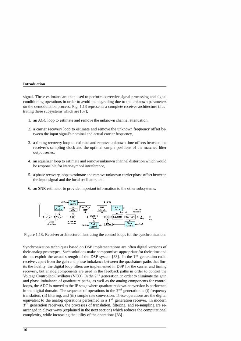
signal. These estimates are then used to perform correctivesignal processing and signalconditioning operations in order to avoid the degrading dueto the unknown parameterson the demodulation process. Fig. 1.13 represents a complete receiver architecture illus-trating these subsystems which are [67];
1. an AGC loop to estimate and remove the unknown channel attenuation,
2. a carrier recovery loop to estimate and remove the unknownfrequency offset be-tween the input signal’s nominal and actual carrier frequency,
3. a timing recovery loop to estimate and remove unknown timeoffsets between thereceiver’s sampling clock and the optimal sample positionsof the matched filteroutput series,
4. an equalizer loop to estimate and remove unknown channel distortion which wouldbe responsible for inter-symbol interference,
5. a phase recovery loop to estimate and remove unknown carrier phase offset betweenthe input signal and the local oscillator, and
6. an SNR estimator to provide important information to the other subsystems.
��� ���
����
����� ��
������
�����
���� ����
�����
��
������
�����
������
����� ��
��
������
��
���������
��������
�����
�����
!����
�����
� "#$%&'(
��
��
��)
��
*&+,%$-('
� "#$%&'(
.+//$(/
0+1(23/
4+5(6+,'
0+1(23/
4$%5
Figure 1.13: Receiver architecture illustrating the control loops for the synchronization.
Synchronization techniques based on DSP implementations are often digital versions oftheir analog prototypes. Such solutions make compromises appropriate for their time anddo not exploit the actual strength of the DSP system [33]. In the 1st generation radioreceiver, apart from the gain and phase imbalance between the quadrature paths that lim-its the fidelity, the digital loop filters are implemented in DSP for the carrier and timingrecovery, but analog components are used in the feedback paths in order to control theVoltage Controlled Oscillator (VCO). In the2nd generation, in order to eliminate the gainand phase imbalance of quadrature paths, as well as the analog components for controlloops, the ADC is moved to the IF stage where quadrature down-conversion is performedin the digital domain. The sequence of operations in the2nd generation is (i) frequencytranslation, (ii) filtering, and (iii) sample rate conversion. These operations are the digitalequivalent to the analog operations performed in a1st generation receiver. In modern3rd generation receivers, the processes of translation, filtering, and re-sampling are re-arranged in clever ways (explained in the next section) which reduces the computationalcomplexity, while increasing the utility of the operations[33].
16

1.6 Modern Receivers - state-of-the-art
Multirate signal processing techniques and CORDIC subsystems deliver efficient solu-tions for synchronization tasks, i.e., carrier recovery, matched filtering, timing recovery,and phase detection.
1.6 Modern Receivers - state-of-the-art
Many companies designing radio receivers and transmittersare still using analog solu-tions which they have directly translated into the digital domain. These legacy designsinclude compromises which were appropriate for their time (e.g., traditional analog fil-ters trading off amplitude- and phase responses for filter order), but it is inefficient tomap such compromises directly into the digital domain. Therefore, new design method-ologies which can lead to more efficient DSP based architectures for digital front-ends,and which can efficiently utilize promising new hardware technologies, e.g., FPGAs, arehighly needed. A digital filter can often perform more than its intended primary filteringtask. It can absorb many of the secondary signal processing tasks of a system. Thereare many ways of folding other functions into the filtering process using multirate signalprocessing techniques, which will be presented here.
In a 2nd generation radio receiver, the sequence of operations (in adigital replica ofthe analog operations performed in a1st generation receiver) is frequency translation, fil-tering, and sample rate conversion. In3rd generation of radio receivers [33], as shown inFig. 1.14, the process of translation and filtering are interchanged according to the Equiv-alency Theorem [30] which states that down-conversion followed by baseband filteringis the same as the filtering at the carrier followed by down-conversion. This reorderingoperation is shown in Fig. 1.15.
����������
���
� ��������� � ���
���� ��
��������
���� ��
��������
���� ��
��������
���� ��
��������
�� ��
������ !"
�#$
%�"�&'���
()*���+�, - .� �/�0 ��� �,
Figure 1.14:3rd generation of radio receiver architecture.
123
456789::
;<=>?@
ABCD
EFGH
IJKLMN
OBCD123
P9QR789::
;<=>?@
ABCD
IJKLMN
EFGISTUV
HOBCD
Figure 1.15: The Equivalency Theorem - down-conversion followed by baseband filteringis the same as filtering at the carrier followed by the down-conversion.
So, rather than moving the desired band to baseband with a complex digital heterodyne,
17

Introduction
the baseband filter is moved to the desired center frequency and filtering is performedto reduce the bandwidth at the digital IF frequency. The resultant reduced bandwidth,complex IF signal is image free and can be down-sampledM -to-1, to its appropriateNyquist ratefs/M . The down-sampling results in aliasing of the center frequency toa new spectral position. The down-sampling can alias the IF frequency directly to thebaseband provided that the IF frequency is positioned at a multiple of the output samplerate [30]. A signal having an offset from a multiple of the output sample rate is alsoaliased to baseband plus that offset. This offset can then beremoved with a carrier re-covery scheme while operating at the reduced sampling rate.The rearrangement of theprocesses is shown in Fig. 1.16 which results in the advantage that the spectral translationnow occurs after the filtering and at the low output rate rather than before the filtering atthe high input rate [33].
�
��������� ���
�����������
�������
����� !"
#
Figure 1.16: Reordering process that moves the down-conversion after the filtering andresampling process.
TheM -to-1 down-sampling after the filtering at IF discards the processed samples whichwastes the computational power used by the filter. To reduce this workload, the resam-pling and the filtering operations are reordered so that one output is computed for everyMinput samples. This is achieved by applying the Noble identity as was shown in Fig. 1.5which requires the original up-converted filter to be partitioned toM subfilters. The re-ordering of theM -partitioned subfilters (lowpass filter) and resampler using the NobleIdentity results in a polyphase filter, as shown in Fig. 1.17.It has the resampler at theinput (a rotary switch which, as previously mentioned, is denoted by the commutator)feedingM subfilters one at a time which operate at the reduced output rate rather thanthe original input rate. As the subfilters operate sequentially, they can be merged into asingle path structure having a subfilter that accesses the coefficients of the successiveMsubfilters.
$%&'()*&+)
,&+)
$-&'()
$.&'()
$/(0-1&'()
234
234
234
5
6
,&+7),&+7)
89:;<=>?@ 8>ABCBC9D@EF9G<>?? HC:B@A
$%&')
*&+)
$-&')
$.&')
$/(0-1&')
6
IJ<>B= 89:;<=>?@F9G<>?? HC:B@A
K; ><<:;CDLM9N:@ OE@DBCB;
7
Figure 1.17: Polyphase partitioning of a lowpass filter usedto apply the Noble Identity toform anM -path polyphase filter.
The lowpass version of a polyphase filter can be converted to its bandpass version by
18

1.6 Modern Receivers - state-of-the-art
associating the complex heterodyne term of the modulation of the filter weights with thedelay elements storing the filter weights. This is achieved by feeding the complex scalarejkr(2Π/M) to each path of theM -path filter [30], wherer is the number of the polyphasepath, andk is the number of channel to be extracted at the baseband. Thisis shown inFig. 1.18.
��������� ������
����
����
����
������
�����������
)2(0 Mkje π
)2(1 Mkje π
)2(2 Mkje π
)2()1( MkMje π−
Figure 1.18: ResamplingM -path down-converter.
The down-sampling process provides a unique feature of changing the phase of the sam-ple locations in the down sampled time series relative to theepochs in the series. In anM -to-1 down sampling, the output time series can be accessed withM different samplephase offsets. TheseM possible output series can effectively be used for a timing recov-ery process. In such a case, the timing recovery loop controls the phase of the re-samplingprocess in the re-sampling filter rather than the loop modifying the locations of samplepoints during the ADC process as done in1st and2nd generation receivers. The phaseof the re-sampling filter is defined by the selection of the phase weights in its single pathstructure. Timing recovery is achieved by controlling an index pointer in the filter’s co-efficient space. For a timing recovery process, the number ofthe polyphase stages (for apolyphase filter) must be increased to satisfy the required timing granularity rather thanthe down sampling requirement [33].
The re-sampling process in the polyphase filter (effecting both the spectral translation andthe timing recovery process), results in a complex basebandsignal at a reduced samplerate and with the correct timing. However, it does not have the correct carrier frequencyand phase correction, which is subsequently corrected by a complex heterodyne operationbefore performing further processing by the equalizer and matched filter. The heterodyneon the complex baseband signal requires four multipliers ascompared to the heterodyneon the real IF centered signal that requires only two multipliers. The complex multipliercan be embedded in the Direct Digital Synthesizer by using the CORDIC algorithm as avector rotator [43] which not only provides the complex samples of the rotating phasorbut performs the multiplication at the same time.
Furthermore, in anM -path polyphase filter, the output sample rate of the baseband aliasedcenter frequencies is always equal toM . TheM -path polyphase filter bank can also bemodified to allow resampling by arbitrary ratios while simultaneously performing base-
19

Introduction
band aliasing from center frequencies at Nyquist zones thatare not multiples of the out-put sample rate. These resampling technique are explained in [69] which embed theresampling process in (i) the polyphase commutator, that is, in the interaction betweeninput data registers and the polyphase coefficients, and (ii) the interaction between thepolyphase outputs and the FFT input. This only requires a state machine to schedule theinteractions, hence there is no computational overhead.
1.7 Polyphase Filter Bank Mapping - State-of-the-Art
We have explored and presented algorithms/ techniques for performing the DFE process-ing tasks for modern SDRs. Multirate signal processing based algorithms turned out tobe a valuable approach for efficient SDR processing engines.An M -path polyphase filterhasM parallel branches, each operating at1/M of the input rate. ThisM -paths paral-lelism can be exploited in a number of different ways to meet the desired cost function ofarea, time, power, etc. The mapping of these parallel structures to highly complex recon-figurable platforms (FPGA) demands a structured methodology to obtain not only a cost-function constrained implementation, but also to exploit enhanced mapping strategies.The state-of-the-art for mapping of polyphase filter banks to reconfigurable platforms istherefore discussed next.
Egg, Harris, and Dick [70] presented a polyphase filter bank based wideband channelizerimplemented on a Xilinx Virtex-4 FPGA, to extract narrow band channels and further toreconstruct a wider bandwidth channel using perfect reconstruction filter. Melis and Co-moretto [71] considered a 512 MHz polyphase filter bank with overlapping bands for usein a spectrometer. Their design used a Xilinx Virtex-5 FPGA,and the multipliers for thepolyphase filter are based on CLB resources. Berner and Leon [72] discussed the FPGAimplementation aspects of a polyphase filter bank as analysis and synthesis filter banks.Valdes et al. [73] showed a polyphase filter bank implementation in MP3 decoding byusing 32-point DCT-II and windowing functions. Marinova etal. [74] presented a mul-ticarrier modem core on an FPGA which uses Offset QuadratureAmplitude Modulation(OQAM) and polyphase filter based analysis and synthesis filter banks. Han [75] analyzedthe front-end design for a wideband SDR. A 32 channel DFE using a polyphase filter bankwas implemented on a Xilinx Virtex-5 FPGA. In [76], Ang et al.showed a Virtex FPGAimplementation of a polyphase filter for sample rate conversion. They presented opti-mizations in terms of transformation to reduce the criticalpath, and constant coefficientmultiplier for both area and speed performance improvement. Fahmy and Doyle [77]suggested an FPGA based reconfigurable polyphase filter bankarchitecture for spectrumsensing which is based on a shared MAC structure. Harris, Vuletic, and Lowdermilk [34]presented a polyphase filter bank based design to replace multi-channel analog modu-lators, where 384 FM modulators are implemented on a single Xilinx Virtex-4 FPGA.Wang et al. [78] showed an energy-efficient hardware architecture and VLSI implemen-tation of a polyphase channelizer with applications to subband adaptive filtering. Theyused the Computation Sharing Differential Coefficient (CSDC) method to obtain a lowcomplexity parallel multiplier-less implementation of FIR subfilters.
In most of the above mentioned literature, the mapping of thepolyphase filter (banks) to
20

1.8 Thesis formulation
an FPGA is presented as a final result emphasizing reduced resource usage, but often theylack a discussion of how these results are actually achievedon highly complex platformswhich provide a huge design space. On the other hand, Intellectual Property (IP) coresare available from different vendors, e.g., [22] [79] [80] [81], these can be customizedaccording to our needs and can eliminate to a certain extend the need for design space ex-ploration. Normally, these IP cores are available for fixed functionalities (i.e., polyphasedecimators and polyphase interpolators) which operate in afixed mode where the samplerate is either decreased or increased by a factor equal to thenumber of polyphase par-titions. The IP cores, are considered to be the future approach to FPGA solutions [82],currently lack advanced multirate signal processing engines that allow several functionsto be embedded within a single filter. These functions include embedded sampling ratechanges that allow any rational sample rate change while simultaneously performing fil-tering operations, combined arbitrary resampling, match filtering, and symbol timing re-covery, etc. As a natural consequence, we therefore formulated our hypothesis to addressthis missing work.
1.8 Thesis formulation
So far we have discussed many technical aspects of modern radio receivers, and we haveconcluded that traditional legacy design can be beneficially replaced by Software DefinedRadios. In order for such devices to operate efficiently, both from a numerical robustnessprospective and from a computational complexity point of view, we have to map theassociated signal processing algorithms onto advanced HW/SW platforms, which is notnecessarily a trivial task. As a consequence, we therefore realized the need for givingsound answers to the following two questions:
1. How do we map the polyphase filter banks onto reconfigurableHW/SW platforms,which normally implies a huge solution space exploration, such that the cost func-tion metrics are simultaneously minimized?
2. Is it possible to embed additional signal processing functions into the polyphasefilter bank, and if so, how is the mapping process efficiently performed with respectto the cost function?
Based on these questions, the thesis is formulated as:
Is it possible to design polyphase filter bank engine(s) performing multiple functionsfor a SDR DFE while achieving cost effective mapping to reconfigurable platform interms of Area, Time, operating clock Speed, and Power consumptions?
In order to investigate this thesis, the following goals have been defined:
1. to explore the design space by taking advantage of the reconfigurable target archi-tecture and
2. to carry out mapping experiments in order to gain sufficient experiences that I canformulate a set of structured design guidelines.
21

Introduction
1.9 Outline of the Dissertation
The remainder of this dissertation is organized as follows:First, the methodology forthe design space exploration for polyphase filter bank basedSDR DFE is described inChapter 2. In Chapter 3, the summary of our contributions is given. This is followed bythe conclusion and outlook in Chapter 4. Chapter 5 gives an overview of the papers A-Fwhich are the contributions to the dissertation. We will refer to these papers by givingthe letter in brackets, e.g., [A]. Citations of other references are numbers within brackets,e.g., [1].
22

2 Design Space Exploration of Polyphase FilterBanks for High Performance SDR Front-Ends
In chapter 1, the enhanced algorithms/ techniques based on polyphase filter banks fordesigning DFE are presented. A generalM -path polyphase filter operating atM timesthe reduced rate than the input sampling rate, still uses thesame number of hardwareresources such as registers, and multipliers (the exception being the number of adders).TheM paths in anM -path polyphase filter provide parallelism which can be exploited ina number of different ways that will be discussed in this chapter. The FPGA takes advan-tage of this inherent parallelism in the algorithm. Furthermore, the rich architecture ofmodern FPGAs provides a large number of choices to map a design, which creates a hugedesign space. It is therefore of great importance to analyzethe building components ofsystem (polyphase filter bank) functionalities with the purpose of determining their possi-ble performance and the cost of applying different processing elements which are presentin the FPGA platform. This task is called Design Space Exploration (DSE). The bestdesign mapping fulfils the requirements and constraints while minimizing the cost func-tion which can be either one or a combination of area, time, power, numerical precision,implementation effort, etc. The mapping often requires several iterations which leadsto a longer development time. This not only costs more money,but also increases thetime to market. This chapter presents the detailed analysisof the polyphase filter (bank)structures and the step-wise refinements in their hardware architectures. The proposedarchitectures form an essential part of the contribution inthis thesis. The outcome of thisDSE and its step-wise refinements can lead to the developmentof Intellectual Property(IP) cores for polyphase filter (banks) that will be beneficial for SDR front-end researchand development.
2.1 Polyphase Filter Structures
An M -path polyphase filter consists ofM parallel subfilters. The data is fed by a ro-tary switch called a commutator and the output is taken afterthe DFT (FFT) operation.Fig. 2.1a shows theM -path polyphase filter where theM -point DFT is replaced by aM -input adder. The commutator is aM -to-1 sampler or a demultiplexer, feeding data to eachof the subfilters that operate atM -times the reduced rate as compared to the incomingsampling rate. The DFT block constructs the individual channels from the down-sampleddata. TheM -path parallelism in aM -path polyphase filter can be exploited to achieveseveral possible structures such as symmetric structures,and serial polyphase structure
23

Design Space Exploration of Polyphase Filter Banks for HighPerformance SDRFront-Ends
with serial and/or parallel MACs.
����
�����
���
��� ���
���� � ������
������������
��� !"!#$%&'"$('
)*+,&-"$(./$,,&0&$1"'
23.
�����
���
���� � ������
������������
4
5
265
789:;9<7==<
>=?=9@=7==<
ABCDEF���
4
5
GHIJKLMN*"O*" ,/('*+,&-"$( 265
N*"O*" ,/('*+,&-"$(64
���
)*+,&-"$(./$,,&0&$1"'
���
)*+,&-"$(./$,,&0&$1"'
./1"(/-
PQQ�RSSTUVR WXYZ[R\XSZR�S
]^RYYX_XR�Z �R`^�a
)*+,&-"$('bN*"O*"
./1"(/-
PQQ�RSSTUVR WXYZ[R\XSZR�S
]^RYYX_XR�Z �R`^�a
./1"(/-
cF
)$(&!-23.
d!(!--$-23.
efg
ehg eig
ejg ekg
3ll$(6m($$ n$"o/(p )*+,&-"$('bN*"O*"
���
����
����
����
Figure 2.1: Different architectural structures of a polyphase filter: (a) General PolyphaseStructure, (b) Symmetric Structure, (c) Adder Shared Symmetric Structure, (d) SerialPolyphase Structure with Parallel MAC, and (e) Serial Polyphase Structure with SerialMAC.
The general polyphase filter structure hasM subfilters of lengthN/M , whereN is thelength of a non-partitioned low pass filter, each operating at 1/M times the input rateas shown in Fig. 2.1a. The symmetric structure utilizes the symmetry of the coefficientsin the subfilters, and therefore reduces the number of subfilters and commutator lengthto M/2 [83]. The commutator moves in both the forward and reverse feed directionsas shown in Fig. 2.1b. In this structure, the multipliers areshared by the two subfil-ters. The adders can also be shared by using multiplexers andde-multiplexers to form anadder shared symmetric structure as shown in Fig. 2.1c. The clock requirements for thesymmetric and the adder shared symmetric structures are doubled i.e.,(fs/M) × 2, ascompared to the general polyphase structure because of the subfilter sharing and reducedcommutator length. In aM -path polyphase filter, only one subfilter is processed at a timeand the remainingM -1 subfilters are idling. The serial polyphase structure takesadvan-tage of this feature and merges the subfilter’s data registers and coefficients to form banksof data registers and coefficients, respectively. These banks are addressed by a controlsequence to select the desired subfilter’s data registers and coefficients to perform MACoperations. The MAC operations can be performed in parallelor in a serial fashion to
24

2.2 Comparative Analysis
form a serial polyphase structure with parallel MAC or with serial MAC [84] as shown inFigures 2.1d and 2.1e, respectively.
2.2 Comparative Analysis
A comparative analysis in terms of resource complexities and clock rates is performedfor aN tap prototype filter which is partitioned into aM -path polyphase filter, each pathwith N/M taps, for the following structures: (i) general polyphase structure, (ii) symmet-ric structure, (iii) adder shared symmetric structure, (iv) serial polyphase structure havingserial MAC, and (v) parallel MAC. Their resource complexities and the respective re-quired operating clock rates are tabulated in Table 2.1. A trade-off is seen between thecomplexities versus the processing clock rates. The serialpolyphase with serial MACshows the least complexity but demands a high clock rate of(fs/M) × N , whereas theserial polyphase with parallel MAC has a slightly higher complexity but operates at a in-put clock rate offs. Similar analyses of these complexities for a 30-tap filter (partitionedinto 5-path polyphase filters, each path with 6 taps), and a 960-tap filter (partitioned into48-path polyphase filters, each path with 20 taps) are presented in our papers [B] and [D],respectively.
Table 2.1: Comparative analysis in terms of resource complexities and clock rates forgeneral polyphase structure, symmetric structure, adder shared symmetric structure, serialpolyphase structure having serial MAC, and parallel MAC.
General Symmetric Symmetric Serial SerialStructure Structure Structure Polyphase Polyphase
(Adder Shared) (Serial MAC) (Parallel MAC)Multipliers N N/2 N/2 1 N/MAdders ((N/M)-1)M ((N/M)-1)M ((N/M)-1)M/2 1 (N/M)-1Registers N N 2N N+1 N+2(N/M)Multiplexers 0 0 N-(M/2) (N/M)+1 N/MDemultiplexers 0 0 M/2 0 0Clock Rate fs/M (fs/M )2 (fs/M )2 (fs/M )N fs
Any of these structures can be selected depending upon the allowed complexity and clockrate. The resource complexity of a generalM -path polyphase filter is the same (except foradders) as for a conventionalN -tap FIR filter, but each subfilter in theM -path polyphasefilter operates at a reduced clock rate offs/M . This reduced clock rate operation leadsto reduced dynamic power consumption which for the normallyapplied CMOS technol-ogy is proportional to the operating clock rate (toggle frequency), as described by thefollowing equation [85]:
Pdynamic = nCV 2f (2.1)
wheren is the number of nodes being toggled,C is the load capacitance per node,V isthe supply voltage, andf is the toggle frequency.C andV are device parameters whereasn and f are design parameters.V can also be a design parameter for the voltage-scalescenario, but we do not consider it further.
25

Design Space Exploration of Polyphase Filter Banks for HighPerformance SDRFront-Ends
On the other hand, the serial polyphase structure with parallel MAC hasM times re-duced resource complexity as compared to the general polyphase structure except for thenumber of registers which is the same for both, but at the sametime it requires aM timeshigher clock rate (i.e.,fs for the subfilter’s processing) as compared tofs/M for thegeneral polyphase structure. It is interesting to note thatone parameter of the dynamicpower equation i.e.,n which is related to area is decreased while the other parameter f isincreased. Since dynamic power is proportional to both of these two parameters, theoret-ically the general polyphase and the serial polyphase with parallel MAC have almost thesame dynamic power consumption. So, the serial polyphase structure with parallel MACreduces the complexity while operating at an input clock rate offs and having almost thesame dynamic power consumption as the general polyphase structure.
A general polyphase structure where each subfilter operatesat a reduced rate offs/Mis a highly desirable solution for very high speed digital front applications as explainedfor an ultra wideband 1.6 GHz channelizer in [70]. The current technology platforms,FPGAs, are not capable of processing at GHz clock rates; however, the parallelism of-fered by multirate signal processing and the polyphase filter bank offers a filter structurewhere subfilters can be realized by current technology platforms while operating at a re-duced clock rate. The highest clock rate supported by the latest FPGAs such as Virtex-7is 700 MHz. However, the internal hardware architecture would limit the maximum oper-ating frequency of the design. The unique feature of polyphase filter banks being mappedas a general polyphase structure is used in our paper [F], where a variant of a polyphasechannelizer which accommodates the spectral shift of multiples of quarters of the channelspacing [30], is used as bandpass filters for a dual-standard(UMTS & WLAN) front-end.It splits the data into multiple paths, operates the subfilters at a lower rate than the in-put sample frequency, and eliminates the need for an IQ demodulator. Although the bestuse of the polyphase channelizer in this case would be to directly extract the individualchannels of both standards rather than splitting the bands followed by separate channel-izes. The approach uses a standard polyphase filter bank (modulated filter banks) wherethe (extracted) individual channel bandwidth is an integermultiple of the input samplerate. The advanced polyphase filter bank approaches mentioned by [65] which filter andsimultaneously down convert multiple signals having arbitrary bandwidths and randomlylocated center frequencies, can be used for a highly efficient solution.
2.3 Subfilter Architectures
The basic block of a polyphase filter is a subfilter implemented as a FIR filter, with dataand coefficient register banks in the case of a serial polyphase structure. There can beseveral different algorithms or techniques for implementing a FIR filter such as FIR fil-tering using parallel multipliers and accumulators, a bit-level systolic array, DistributedArithmetic, Fast FIR algorithms, Frequency domain filtering, Multiplier-less FIR filter(SOPOT), etc. The most direct approach of performing a FIR filter’s operation is byusing parallel multipliers and accumulator (MAC). Today’sFPGAs have dedicated mul-tipliers (e.g., DSP48E slices in Xilinx FPGAs) which are designed especially for highspeed and low power consumption. They are generally highly preferred for the filter’sMAC operation instead of a CLB-based MAC.
26
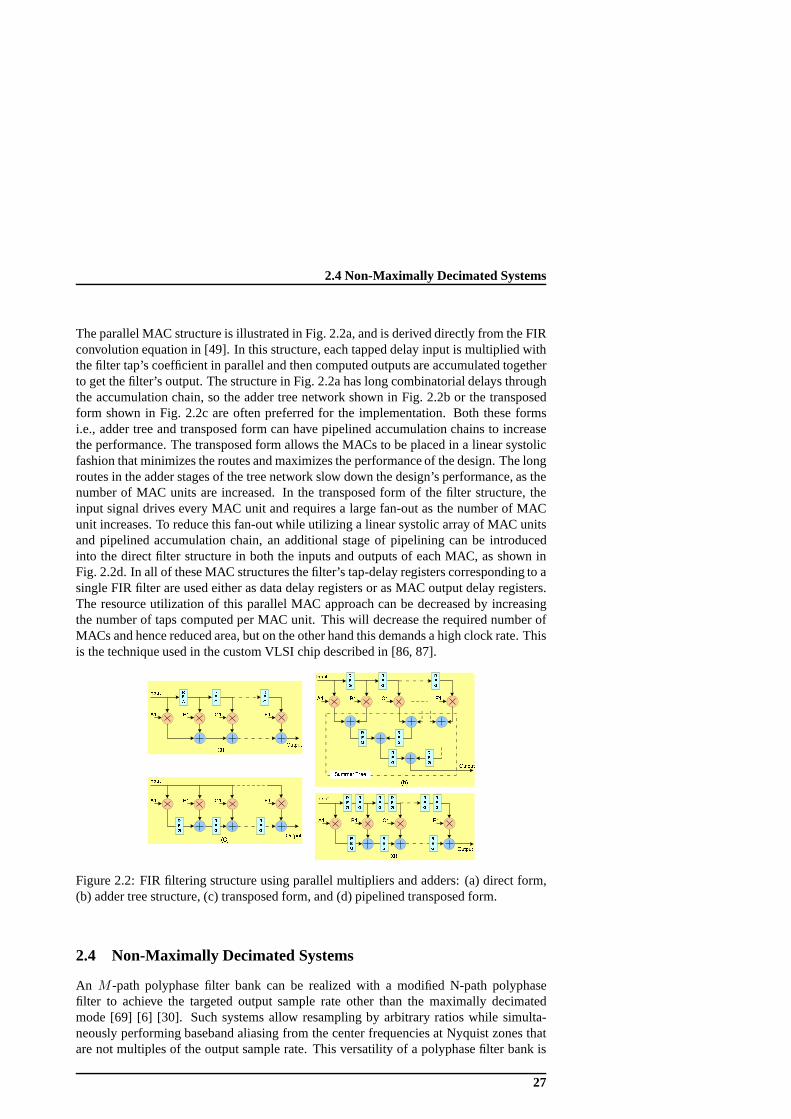
2.4 Non-Maximally Decimated Systems
The parallel MAC structure is illustrated in Fig. 2.2a, and is derived directly from the FIRconvolution equation in [49]. In this structure, each tapped delay input is multiplied withthe filter tap’s coefficient in parallel and then computed outputs are accumulated togetherto get the filter’s output. The structure in Fig. 2.2a has longcombinatorial delays throughthe accumulation chain, so the adder tree network shown in Fig. 2.2b or the transposedform shown in Fig. 2.2c are often preferred for the implementation. Both these formsi.e., adder tree and transposed form can have pipelined accumulation chains to increasethe performance. The transposed form allows the MACs to be placed in a linear systolicfashion that minimizes the routes and maximizes the performance of the design. The longroutes in the adder stages of the tree network slow down the design’s performance, as thenumber of MAC units are increased. In the transposed form of the filter structure, theinput signal drives every MAC unit and requires a large fan-out as the number of MACunit increases. To reduce this fan-out while utilizing a linear systolic array of MAC unitsand pipelined accumulation chain, an additional stage of pipelining can be introducedinto the direct filter structure in both the inputs and outputs of each MAC, as shown inFig. 2.2d. In all of these MAC structures the filter’s tap-delay registers corresponding to asingle FIR filter are used either as data delay registers or asMAC output delay registers.The resource utilization of this parallel MAC approach can be decreased by increasingthe number of taps computed per MAC unit. This will decrease the required number ofMACs and hence reduced area, but on the other hand this demands a high clock rate. Thisis the technique used in the custom VLSI chip described in [86, 87].
�� �� �� ��
����
����
�
�
�
�� �� �� ��
����
����
�
�
�
�� �� �� ��
����
����
�
�
�
�
�
�
�
�
�
������ ����
�� �� �� ��
����
����
�
�
�
�
�
�
�
���
���
���
���
Figure 2.2: FIR filtering structure using parallel multipliers and adders: (a) direct form,(b) adder tree structure, (c) transposed form, and (d) pipelined transposed form.
2.4 Non-Maximally Decimated Systems
An M -path polyphase filter bank can be realized with a modified N-path polyphasefilter to achieve the targeted output sample rate other than the maximally decimatedmode [69] [6] [30]. Such systems allow resampling by arbitrary ratios while simulta-neously performing baseband aliasing from the center frequencies at Nyquist zones thatare not multiples of the output sample rate. This versatility of a polyphase filter bank is
27

Design Space Exploration of Polyphase Filter Banks for HighPerformance SDRFront-Ends
presented in our paper [A] by utilizing five different resampling factors. These resamplingcases correspond to: (i) maximally decimated, (ii) under-decimated, (iii) over-decimated,and combined up- and down-sampled with (iv) single, and (v) multiple stride length sce-narios. The resampling technique is based on sliding cyclicdata loading interacting withcyclic shifted coefficient memory [69].
A non-maximally decimated polyphase filter bank, where the number of data loads is notequal to the number ofM subfilters and processesM subfilters in a time period which iseither less or greater than theM data loads. The embedded resampling in the polyphasefilter banks requires architectural changes for the structures presented in Fig. 2.1 to meetthe required time constraint. These changes mainly apply tostructures which share re-sources such as symmetric structure and serial polyphase structures. A general polyphasestructure is a fully parallel solution and is operationallynot affected in non-maximallydecimated modes because each subfilter is operating independently andM subfilters canbe processed even within a single data input time period. However, it does require somechanges in its state machine. Symmetric structures are limited to cases with an even num-ber of polyphase partitions to make use of filter symmetry, which is not the case for serialpolyphase structures. In our further discussion, we focus on the serial polyphase structurewith parallel MAC for non-maximally decimated polyphase filter banks.
In the serial polyphase structure with parallel MAC, as shown in Fig. 2.1d, the data andthe coefficients registers are merged to form respective banks and share the same MAC ina parallel configuration. The realization of the data register bank is challenging as it has toshift the new data element to the respective subfilter’s tap-delay line and having access toall the taps of that subfilter at the same time. In the case of a maximally decimated system,where the down-sampling factor is equal to the polyphase partition, FIFOs can be usedas delay lines to derive an optimal structure, as described in [88], operating at the inputdata rate. The non-maximally decimated systems (under-decimated, over-decimated, andcombined up- and down-sampling with single and multiple stride length of the commuta-tor), require a two dimensional memory based solution whereonly the targeted subfiltercan be loaded with the input data.
2.5 Optimizations for Area Resources
There exist a number of design options depending upon the usage of the FPGA resources.Today’s FPGAs have rich architectures with special memory resources such as distributedRAMs and block RAMs, and high performance computational resources such as DSP48Eslices in addition to the basic CLBs. The DSP48E slice provides not only improved flexi-bility and utilization, but also reduced power consumption, increased operating frequency,and reduced set-up and clock-to-out time. The efficient usage of these dedicated resourcescan result in a high performance system in terms of achievinghigh operating clock ratesand reduced CLB requirements.
A straightforward mapping of the polyphase partitioned data register bank is to use CLBslice registers to form individual subfilter’s delay lines which are connected to multiplex-ers to form a register bank as shown in Fig. 2.3. This solutioncan be suitable for a small
28

2.5 Optimizations for Area Resources
filter because even a small filter results in a relatively highresource utilization of theCLB’s slice registers and LUTs. The resource utilization will scale linearly with the filtersize.
������
�����
���
����
�����������
����� �������� �����
! "#$ %�!�&
' (((((() *+"
"
,-./0-1 ' (((((() *+"
' (((((() *+"
Figure 2.3: Data register bank formed by individual shift register arrays, multiplexers,and decoder.
In our papers [B] and [D] different design options for a register bank mapping on a Virtex-5 FPGA by exploiting its resources such as slice registers, RAM based shift register, dis-tributed RAM, and block RAM are presented. Fig. 2.4 illustrates the mapping options fora24× 40 register bank [D] (40 rows and 24 columns register bank with 32-bits complexdata register). Fig. 2.5 presents their resource usage in terms of the CLB’s slice registersand LUTs. The straightforward mapping of a register bank which is the structure shownin Fig. 2.3 uses 47% and 21% of the slice registers and LUTs, respectively. This is onlyfor real data and therefore the numbers would be double this for complex data. Next, eachdata register in the subfilters is replaced by a RAM-based shift register (SRL16 / SRL32mode of the slice LUTs) and the resource utilization (for real data only) comes out to be0% and 21% for slice registers and LUTs, respectively. This eliminates the need for theslice registers, but the LUT usage is the same as before. In a Virtex-5 FPGA, each CLBhas 64-bit distributed RAM [89], but it is bit-addressable,so for 16-bit data, 16 CLBs arecollectively used as a single 16-bit register. The rest of the 63 bits in each CLB remainunused. Based on this analysis, distributed memory is used such that each64-bit memorycontributes 1-bit to a 16-bit data element for 64 subfilters (only 40 are used here) as shownin Fig. 2.4. So the memory which was previously used for only one subfilter is now beingused for all the 40 subfilters. The bit-width is further extended to32-bits to incorporatecomplex data (16 + 16 bits), and the resource utilization dramatically decreases to 2%both for slice registers and LUTs (for complex data). This will also eliminate the need forthe decoder and multiplexers to select the desired subfilter’s data elements in the case ofa shift register based register bank. The same concept is further applied to block RAMs,which completely eliminates utilization of the CLBs. The block RAMs utilization fora 40 × 24 register bank is 12 block RAMs, which corresponds to 9% utilization for aVirtex-5. A similar analysis for a5× 6 register bank is presented in our paper [B].
The distributed RAMs and block RAMs can efficiently replace each column of the dataregister bank and their cascade can form a complete registerbank as shown in Fig. 2.6.This reduces the resource usage but at the same time it requires loading of the new data
29

Design Space Exploration of Polyphase Filter Banks for HighPerformance SDRFront-Ends
� � ��
������ ������
������ ��������� ���
� ���
�
��
�� ���
�
��
�
������ ��������� ���
��
���� �������� ���
�!
Figure 2.4: Data register bank mapping options in the Virtex-5 FPGA.
0
2000
4000
6000
8000
10000
12000
14000
16000
16-Bits x 1Slice Registers
16-Bits x 1RAM Registers
32-Bits x 40 Distributed RAM
32-Bits x 40 Block RAM
No
. of R
eso
urc
es
Slice Registers
Slice LUTs
Figure 2.5:40× 24 register bank resource usage by using slice registers and LUT, RAMregisters, distributed RAM, and block RAMs.
element to memory and shifting the previous data to the next cascaded memory stage.
"#
$%&% '()*+&(, -%./
#0
1232
2114
54
67 68 69 69:
;<=>? @ ABCDEFGH
IJ
KL MNNL
OPQ
;<=>? @ ABCDEFGH
IJ
KL MNNL
OPQ
;<=>R<ST>UVFGH
IJ
KL MNNL
OPQ
Figure 2.6: Realization of complete register bank by using cascade memories (distributedRAMs or blockRAMs).
A block RAM based register bank which does not require any CLBresources needs anextra clock cycle for each data load and shift, as described in our paper [D]. The reason isthat the data shift in the subfilters requires data to be available from the preceding memorywhich requires one clock cycle to read the data element. The next clock cycle will loadthe new data element along with shifting of the subfilter. This is due to the fact that blockRAMs have synchronous write and read operations. On the other hand, a distributed
30

2.6 Architecture Exploration
RAMs based register bank has no extra clock cycle penalty foreach data load and shift(provided that there is no input/output register) as such memories have asynchronous readand synchronous write operation. The filter coefficient bankcan also be realized by theresource options presented in Fig. 2.5. However, it does notrequire the shifting as wasnecessary for a data register bank.
2.6 Architecture Exploration
Among the embedded resampling scenarios presented in our paper [A], the cases wherethe number of data loads is less than the number of subfilters (M ) which are under-decimated and combined up- and down-sampling with single stride length of commuta-tor, the run-time processing at the input sample ratefs for serial polyphase structure withparallel MAC is not possible. One solution is to operate the polyphase engine at a higherclock rate and interface to the input data at a lower rate by using a FIFO.
A Load-Process Architecture (LPA) with block RAM based register bank (LPA-BR) fora polyphase filter bank operating in the under-decimated mode is presented in our paper[D]. It has 48- and 40-path polyphase filter banks for up- and down-sampling channeliz-ers, respectively. Fig. 2.7 shows the architecture for the down-sampling channelizer withan output accumulator instead of an FFT, representing the channel at the baseband. It usesa common address bus for all the cascaded block RAMs which corresponds to individualtaps of the subfilters, whereas the 48-path up-sampling channelizer requires a distributedaddress bus (5 distinct address pointers) for its 20 cascaded block RAMs to achieve itsrequired circular data shift [D].
�������� ���
������ ���
��
��������� ���
���
�������
����
��� ��
!""#$#%&'()
*���
+, &--)
-(#'-./
"%0
12/
3+,45.' 6 789 5%("0 :!;<
&--)
-(#'-./
"%0
12/
3&--)= 12/= "%09
> ,
&--)
-(#'-./
"%0
12/
,7
?@ A�@�AB CBBA� D�AA
EFG7HIJKL JKL JKL
M8 M> M,+>N >N >N
:2&%
O$&P
Figure 2.7: Load Process Architecture with block RAM based register bank for a down-sampling polyphase filter operating in under-decimated mode, running at a clock ratehigher than the input data rate.
During the load phase, the data elements are fed from the input FIFO and loaded to thesubfilters as directed by the data pointer. In the processingphase, coefficient and datapointers having embedded shifts, select the coefficient anddata memory elements to per-form MAC operations. The multipliers are based on DSP48E slices whereas the additionsare performed by using a CLB based adder tree network. The architecture loads the reg-ister bank withN data elements from the input FIFO and then processM subfilters whilethe FIFO is being loaded. As the FIFO is continuously loaded and unloaded only duringthe process cycles, shown in Fig. 2.8a, the FIFO eventually overflows. In order to over-come the FIFO’s overflow and to meet the output time constraints, the polyphase filters
31

Design Space Exploration of Polyphase Filter Banks for HighPerformance SDRFront-Ends
need to run at high clock rates, which are4 times the input clock rates i.e.,4 × 200 MHzand4 × 240 MHz for the up- and down-sample channelizers, respectively. These highclock rate demanding designs are not only difficult to achieve but also the architecturesbecome power hungry, since the dynamic power consumption isproportional to the togglefrequency. The high clock rates for the LPA may limit the use of polyphase filter designsto lower input sample rates.
A reduced sized filter bank channelizer, specifically a5-path polyphase filter with eachpath being6 taps is presented in our paper [A] for different embedded resampling casesand their architectural exploration is performed in our paper [B]. The block RAM basedLPA for the embedded resampling cases presented in our paper[B] shows that on theaverage approximately 60% of the time is used for loading theregister bank from theinput FIFO, which eventually demands high operating clock rates to process the loadeddata within the output time constraints. The high clock ratedemands of LPA-BR can bereduced by using distributed RAM based register banks and byapplying different sched-ules such as interlaced load-process and runtime scheduling. The use of distributed RAMbased register banks in the LPA, reduces the clock rate by 20 to 25% as compared to theirblock RAM based counterparts [B][D].
In LPA with distributed RAM based register bank (LPA-DR), the scheduling of the loadand process cycles can also be improved to further reduce therequired operating clockrates. The idea is to interlace the load process architecture such that the processing of thesubfilters (process-cycle) starts along with the data loading from the FIFO (load-cycle),instead of waiting for the complete loading of the data-loaded (targeted) subfilters beforeprocessing. In this case, the process-cycle continues forM subfilters, but the data loadingis stopped for non data-loaded (non-targeted) subfilters. This is the only time when inputdata is pushed onto the FIFO without being pulled at the same time. Since the numberof non-targeted subfilters is less than the number of targeted subfilters, the FIFO doesnot grow as rapidly as in the previous case where process-cycle starts after completingthe load-cycle as shown in Fig. 2.8a. This interlaced schemefor loading and processingas shown in Fig. 2.8b reduces the overall clock cycles count and therefore reduces therequired clock rate.
���������� ������� ���������� �������
����������
�������
����������
�������
��� ������
��� ������
�������� �
�������
�������� �
�������
���
���
Figure 2.8: Scheduling of load- and process-cycles for (a) LPA and (b) interlaced LPA.
By applying the interlaced scheme to LPA-DR in our paper [C],the required clock ratecan be reduced to2× (twice the input data rate) as compared to3× and4× clock forits LPA-DR and LPA-BR counterparts. In an interlaced LPA, most of the process cycles
32

2.6 Architecture Exploration
which are overlapped by the load cycles are idling as they arewaiting for the next avail-able data from the input FIFO. To make efficient use of these idling cycles of the2×clock, our paper [B] introduces a Run-time Architecture (RA) where non-targeted subfil-ter’s processing is achieved by idling cycles of the2× clock instead of processing themafter the load cycle. The idea is to operate at twice as high a data clock rate, process theinput data while simultaneously loading the subfilters on the first cycle of the2× clockand the next cycle of the2× clock is used to process the non-targeted subfilter. By usingthis scheme, the non-targeted subfilters get processed within the time frame of the tar-geted subfilters and therefore reduce the overheads as in thecase of LPA and interlacedLPA. It also eliminates the need for the input FIFO. The RA scheduling for the embeddedresampling cases are presented in our paper [B] and the RA is shown in Fig. 2.9. It uses adistributed RAM based register bank (without input/outputregisters), a block RAM basedcoefficient bank, and a MAC based on a systolic array of DSP48Eslices.
The parallel data from the data register is delayed by a set ofdelay elements to align thesubfilter’s MAC and final accumulation process within the systolic array MAC as shownin Fig. 2.9. The corresponding delay for the coefficient register bank can efficiently beachieved by offset addressing, instead of using a delay element network. The RA with aDSP48E systolic array based MAC has a large latency due to thepipeline and delay reg-isters, but has an enhanced maximum operating clock rate. The multiplexer block prior tothe delay elements switches between the targeted subfilter’s and non-targeted subfilter’sprocessing, which is used only in under-decimated and combined up and down samplingwith single stride length.
�������
������ �
���
������ � ���
������
���
� ��
!�"#
� $�%
� �� �
&''()(*+,-.
/010
23451
������6 ������7
89:
89;
89<
�=>�
0??@
A@ B@?
��
�� �� ��
C�0D
2E0F
G&HIJKL,-*M'&..+KN
������ �
���
������ � ���
������ �
���
������ � ���
�
OPQ
RS"S$
TS �U
OPQ
OPQ
OPQ
OPQ
OPQ
OPQ
OPQ
OPQ
OPQ
OPQ
OPQ
OPQ
Figure 2.9: Runtime Architecture with a DSP48E systolic array based MAC. The datafrom the register bank is fed through a set of delay elements that delay the parallel dataelement by element to time align the subfilter’s MAC and final accumulation process.
Among the architectures presented in our paper [B], the LDA-BR, LDA-DR, and RA use
33

Design Space Exploration of Polyphase Filter Banks for HighPerformance SDRFront-Ends
DSP48E slice multipliers and a CLB based adder tree for theirMACs, whereas RA with aDSP48E systolic array (RA-DSP48E) uses a DSP48E slice basedsystolic array MAC. Allthese cases with different configurations use a block RAM based coefficient bank. Theresource usage of FPGA mapping for the five embedded resampling cases for their LPAand RAs are presented in [B], in terms of slice registers, slice LUTs, dedicated resources,required operating clock rates, and dynamic power consumptions. The RAs turn out to bea preferred choice to reduce operating clock rates and reduce dynamic power consump-tion. Using RA is also a preferred means to reduce area resources with the exception ofsome cases (under-decimated and combined up- and down-sampling with single stridelength of commutator) which use multiplexers and pre-stored indices in the LUTs for ad-dressing their data and coefficient banks. RA slightly increases the area but on the otherhand, operates at a reduced clock rate as compared to their variants.
The coefficient banks which are based on block RAMs for these architectures can alsobe replaced by distributed RAMs. In this case, the block RAM resources which werepreviously used by coefficient banks are unnecessary and thebits occupy additional CLBresources.
2.7 Optimization for Enhanced Clock Speed Performance
Fig. 2.10 shows an analysis for the best case achievable clock rate for the architectures forthe five cases of embedded resampling presented in our paper [B]. These values are gen-erated under balanced performance design goal and strategies in the Xilinx ISE tool [90].This tool optimizes the design’s place and route to meet the specified timing constraint.All the cases presented have different timing constraints except for the RAs operatingat 2× clock rate. These targeted timing constraints are further tightened to obtain themaximum possible optimization by the tool to achieve the higher clock rates for thesearchitectures. The red dotted horizontal line on each bar graph in Fig. 2.10 shows thetiming constraint of the corresponding case. All the timingconstraints are met except theone for case4, which is the LPA with block RAM based register bank. The LPA-BR,LPA-DR, and RA (in balanced design goal and strategy in Xilinx ISE tool) can executeat up to200 MHz whereas RA-DSP48E (systolic array) can execute at up to350 MHz.This speed enhancement results from the systolic array of a DSP48E slice based MAC.All these architectures have a block RAM based coefficient bank. The clock speed canbe further enhanced by using either distributed RAM or pipelined block RAM based co-efficient banks to300 MHz and400 MHz for the adder tree and the systolic array MACarchitectures, respectively.
The RA for the up- and down-sample polyphase filters presented in our paper [C], op-erating at2× the data clock rate, require processing at400 and480 MHz, respectivelyto meet their output time constraints. The asynchronous path between the cascaded dis-tributed RAMs (without input/output registers) turns out to be a bottleneck with respectto achieving higher clock rates. In our paper [C], it is shownthat as the number of cas-caded distributed RAM (without input/output register) increases, their maximum operat-ing clock rate decreases. On the other hand, a minimum of500 MHz performance can beachieved even with up to24 cascades of distributed RAMs having output registers. The
34

2.8 Explored Solution Space
0306090
120150180210240270300330360390420450
CASE 1 CASE 2 CASE 3 CASE 4 CASE 5
Clo
ck S
pee
d (
MH
z)
LPA-BRLPA-DRRARA-DSP48E
���� ��������
�� ��� ������
Figure 2.10: Best case achievable clock rate performance for the five embedded resam-pling cases; maximally decimated system (CASE 1),Under-decimated system (CASE 2),Over-decimated system (CASE 3), Combined up- and down-sampling with single stridelength (CASE 4) and with multiple stride length (CASE 5).
insertion of an output register for each cascaded distributed RAM forms a pipelined reg-ister bank that allows high operating clock rates, but at thesame time the added registersrequire balancing of the control and data paths and also one tapped-delay shifting for thecascaded distributed RAM (pipelined). These are achieved by inserting the pipeline regis-ters for the control path (i.e., address and read/write signal), and by delaying each memoryoutput path by the total number of cascaded distributed RAMsminus its tap number, asshown in Fig.2.11. The added pipeline register network willadd additional latency whichis a compromise to achieve high operating clock rates. Furthermore, the real and imag-inary register banks are separated and use16-bit memories instead of a combined (realand imaginary) data register bank using32-bits memories. The separate memory banksallow the tool’s place and route process to meet the timing constraints of480 MHz. TheRun-time Architectures are capable to meet the challengingdemands for a modern SDRfront-end in terms of minimal area, time (clock frequency),and power requirements.
2.8 Explored Solution Space
Finally, the explored solution space for designing polyphase filter banks operating in non-maximally decimated modes is presented by a complete flow diagram shown in Fig. 2.12.The flow diagram wraps up every thing we have presented previously and helps to givethe answer to our initial thesis. The processing engines forthe selected serial polyphasefilter structure can be realized by Load-Process and RuntimeArchitectures. Their internalbuilding blocks i.e., data and coefficient register bank canbe mapped, in a straightforwardmanner, to CLB based slice registers or RAM based registers,which results in a high re-source utilization of CLB resources even for a small sized polyphase filter. On the otherhand, the data and coefficient banks can be mapped in a resource efficient manner to blockRAM and/or distributed RAMs. The MAC architecture can be based on summer tree orsystolic array consisting of DSP48E slices.
The design flow provides a mean to explore the trade-off between the targeted constraints
35

Design Space Exploration of Polyphase Filter Banks for HighPerformance SDRFront-Ends
����� ���
�� ���� ���
����
��������
����
����� ��� ����
����
!�"#�
$%&�
�''�
(�
)*
+,-..,
/01
����� ���
�� ���� ���
)*
+,-..,
/01
����� ���
�� ���� ���
)*
+,-..,
/0123
����� �4�
56 ���� ���
789:: 6 789:: 5
����� �4�
� ���� 5�6�
789::;<==>
?�@<>A B8C@�9>
6 5DE�
789::;7@�>
FG�HH�I����
����
789:: � 789:: 5D
����� �4�
� ���� 5�6�
=<�<;<==>
?�@<>A B8C@�9>
6 5DE�
=<�<;7@�>
����
! ��
����
! ��
����� �4�
56 ���� ���
����� �4�
56 ���� ���
����� �4�
56 ���� ���
JKLM
JKLN
JKLL
JKO
JKL
JKO
JKLN
6
�PQ��R
JKO
JKO
JKO
JKO
JKO
JKO
JKO
JKO
JKO
JKO
JKO
JKO
S���G��I
T����
JKO
Figure 2.11: The complete architecture for the down-samplepolyphase filter with 24cascaded Dist. RAMs, delay/pipeline registers, multiplexers, systolic array of DSP48Eslices, coefficients’ distributed ROM, and data and coefficient address distributed ROM.
and the required FPGA resources. The explored architectures for the polyphase filterbank (for its serial polyphase with parallel MAC structure)followed by their step-wiserefinements provide customized solutions for the designersto meet their targeted designconstraints of area, time, and power. A comparison of area, time and power for the ex-plored architectures and their customized solutions for a polyphase filter bank operatingin five different resampling modes is presented in our paper [B]. The LPAs are the mostpower hungry solutions because of their requirements for high operating clock rates. Theinterlaced LPAs provide significant improvements to LPA by reducing the clock rates.The RA while operating at maximum of two times the input rate provides the least powerconsumption solutions. Furthermore, it is seen from Fig. 2.12 that the design customiza-tion results in wide range of operating clock rate performance from200MHz to500MHz.The RA supports the designer’s requirements of minimal area, power, and operating clockrates, while at the same time being capable of achieving highclock rate performance.
Furthermore, an analysis is performed for latency and throughput of the presented archi-tectures. The throughput is constrained by the output sample rates so that it is same forall the architectures under the same resampling case; however, they vary in terms of theirlatencies. A detailed latency analysis is tabulated in Tables 2.2 to 2.6 representing the fivedifferent embedded resampling cases for the polyphase filter bank. The previous timecalculation for the load process architectures as presented in our paper [B], are carriedout on the control signals from their state machines, i.e., controlling the load and processcycles. The loading time was calculated from the non-empty signal from the FIFO, but
36

2.8 Explored Solution Space
�������
��������
�������
��������
������ �������
������� ���
������ �������
������ ���
������� ������ ����
������ �������
��������
sf@
M
f s @
����������
�������
���������� �
����� �������
���
����
M
f s 2 @
!!"
#$$%
&
Msf@ N
��'�����
(�������
)��*��'�����
(�������
)��*��'����� (������� �����
+����*
��������
,-��*
(�������
���.���� ��* ���
��/�*��������
0������ ������ ������1
2���* ����� ���34��������
2���* ����� ���35��*���� ���3
(�����.���� 5��
0���������1
���
������ ����
��'�����
(�������
��'�����
(�������
���
����� ����
67879:;<=8:>?7@A
BC:DD<E<:@89:;<=8:>?7@A
FGB
���.���� ��* ���
��/�*��������
0�������� ������ ������1
���� 5��
G>EH<8:E8I>:=
JKKLMN
OKKLMN
(�����.���� 5��
(�����.���� 5�� P
�������� ���� 5��
(�����.���� 5��
���� 5�� ���� 5��
(�����.���� 5�� P ��������
���� 5��
(�����.���� 5�� P
�������� ���� 5��
OQKLMN
RKKLMN
QKKLMN
���
������ ����
sf@2
���
����� ����
JKKLMN
OKKLMN
��'�����
(�������
F7ST
Figure 2.12: Flow diagram based on the explored solutions for designing the polyphasefilter banks operating in non-maximally decimated modes.
37

Design Space Exploration of Polyphase Filter Banks for HighPerformance SDRFront-Ends
the FIFO loading time is not included. Similarly, the process time is calculated from thestate machine’s control signal, but it did not incorporate the processing delay through theMAC operations. These two timing parameters do not effect the results presented in ourpaper [B] in Table 2 and Table 3, but they do have an effect on the latency, which are nowtaken into consideration.
Table 2.2: Case 1 (Maximally Decimated): Latency and clock cycles distribution fordifferent architectures.
LPA-BR LPA-DR RA RA (Systolic Array)
Clock Period (ns) 6.66 8.33 33.33 33.33Latency - Time (ns) 246.7 258.3 333.33 466.7
Latency - Clock Cycles 37 31 10 14Clock Cycle Distribution
FIFO Load/Unload + 24 19 - -Data Register Bank Load -
State Machine’s Overhead 2 2 - -(load and process) -
Data Register Bank Read 1 - - -MAC - Adder Tree
Multiply 1 1 1 -Adder Tree(log2(N/M)) 3 3 3 -
MAC - Systolic ArrayMultiply pipelined delay - - - 3
Delay across Array(N/M − 1) - - - 5Subfilter to be processed 5 5 5 5
M-input Accumulation 1 1 1 1
TOTAL 37 31 10 14
It can be seen from Table 2.2 to Table 2.6, LPAs have large latency which basically is dueto the loading cycle. This eventually results in needing high clock rates to meet the tar-geted throughputs. The latency of LPA-BR is larger than the latency of LPA-DR becauseof the fact that block RAM takes one clock cycle to read and will accumulate over thesubfilter’s length during the loading cycle. Similarly block RAMs’ read operation in theprocess cycle has a one clock cycle delay as compared to the case for distributed RAMs.The RA’s simultaneously loading and processing of the inputs, results in reduced latencysolutions. The latency for MAC operation is fixed (dependingon the subfilter’s length)and is the same for all the architectures except the systolicarray based MAC which takes4 extra clock cycles. Furthermore, RAs operating on 2× clock rates take one clock cycleextra to switch between the targeted (data-loading) and non-targeted (non data-loading)subfilters’ processing.
The RA with distributed RAM pipelined register bank, distributed RAM or pipelinedblock RAM based coefficient bank, and systolic array of DSP48E slices based MAC isa preferred choice in terms of enhanced performance and low latency for state-of-the-artSDR digital front-ends.
It was stated in chapter 1 that high performance radio designs (which is also true for
38

2.8 Explored Solution Space
Table 2.3: Case 2 (Under-Decimated): Latency and clock cycles distribution for differentarchitectures.
LPA-BR LPA-DR RA RA (Systolic Array)
Clock Period (ns) 5.55 6.66 16.66 16.66Latency - Time (ns) 161.1 160/166.7 183.3 250
Latency - Clock Cycles 29 24/25 11 15Clock Cycle Distribution
FIFO Load/Unload + 17 12/13 - -Data Register Bank Load -
State Machine’s Overhead 2 2 - -(load and process) -
Data Register Bank Read 1 - - -Multiplexer - - 1 1
MAC - Adder TreeMultiply 1 1 1 -
Adder Tree(log2(N/M)) 3 3 3 -MAC - Systolic Array
Multiply pipelined delay - - - 3Delay across Array(N/M − 1) - - - 5
Subfilter to be processed 5 5 5 5M-input Accumulation 1 1 1 1
TOTAL 29 24/25 11 15
Table 2.4: Case 3 (Over-Decimated): Latency and clock cycles distribution for differentarchitectures.
LPA-BR LPA-DR RA RA (Systolic Array)
Clock Period (ns) 8.33 11.11 33.33 33.33Latency - Time (ns) 308.3 333.3/322.1 366.7 500
Latency - Clock Cycles 37 30/29 11 15Clock Cycle Distribution
FIFO Load/Unload + 24 18/17 - -Data Register Bank Load -
State Machine’s Overhead 2 2 - -(load and process) -
Data Register Bank Read 1 - - -MAC - Adder Tree
Multiply 1 1 1 -Adder Tree(log2(N/M)) 3 3 3 -
MAC - Systolic ArrayMultiply pipelined delay - - - 3
Delay across Array(N/M − 1) - - - 5Subfilter to be processed 5 5 6 6
M-input Accumulation 1 1 1 1
TOTAL 37 30/29 11 15
39

Design Space Exploration of Polyphase Filter Banks for HighPerformance SDRFront-Ends
Table 2.5: Case 4 (Combined up- and down-sampled with singlecommutator stridelength): Latency and clock cycles distribution for different architectures.
LPA-BR LPA-DR RA RA (Systolic Array)
Clock Period (ns) 4.76 5.55 16.66 16.66Latency - Time (ns) 147.5/119 150/122.2 183.3 250
Latency - Clock Cycles 31/25 27/22 11 15Clock Cycle Distribution
FIFO Load/Unload + 18/12 15/10 - -Data Register Bank Load -
State Machine’s Overhead 2 2 - -(load and process) -
Data Register Bank Read 1 - - -Multiplexer - - 1 1
MAC - Adder TreeMultiply 1 1 1 -
Adder Tree(log2(N/M)) 3 3 3 -MAC - Systolic Array
Multiply pipelined delay - - - 3Delay across Array(N/M − 1) - - - 5
Subfilter to be processed 5 5 5 5M-input Accumulation 1 1 1 1
TOTAL 31/25 27/22 11 15
Table 2.6: Case 5 (Combined up- and down-sampled with multiple commutator stridelength): Latency and clock cycles distribution for different architectures.
LPA-BR LPA-DR RA RA (Systolic Array)
Clock Period (ns) 8.33 11.11 33.33 33.33Latency - Time (ns) 375/341.7 400/366.6 433.3/400 566.7/533.3
Latency - Clock Cycles 45/41 36/33 13/12 17/16Clock Cycle Distribution
FIFO Load/Unload + 32/28 24/21 - -Data Register Bank Load -
State Machine’s Overhead 2 2 - -(load and process) -
Data Register Bank Read 1 - - -MAC - Adder Tree
Multiply 1 1 1 -Adder Tree(log2(N/M)) 3 3 3 -
MAC - Systolic ArrayMultiply pipelined delay - - - 3
Delay across Array(N/M − 1) - - - 5Subfilter to be processed 5 5 8/7 8/7
M-input Accumulation 1 1 1 1
TOTAL 45/41 36/33 13/12 17/16
40

2.8 Explored Solution Space
other systems) need both the smart algorithms and their optimized or near optimized im-plementation on the processing platforms. Multirate signal processing based algorithms/techniques for numerous DFE functionalities as explained in Chapter 1 allow low com-plexity design for DFE tasks which can further be implemented in a cost effective manner.Reducing sampling rate of the signal along with the bandwidth reduction (filtering) andsignal processing by effective use of the aliasing process are the distinguishing features ofmultirate signal processing. Furthermore, instead of a normal FIR filter process, this alter-native approach allows distributed processing over a number of subfilters (as a polyphasefilter) and even at a reduced processing rate. These techniques should be adopted bythe state-of-the-art radio transceiver designs and are highly recommended to the systemdesigner of SDR based DFE designs including:
Single and multiple channel extraction and filtering,
With equal and unequal channel (spacing) distribution,
Embedded (rational) sample rate conversion,
Arbitrary sample rate conversion, and
Combining multiple tasks into a single processing filter.
A polyphase filter structure capable of combining multiple tasks (i.e., arbitrary resam-pling, match filtering, and symbol timing recovery) is presented in our paper [E].
This dissertation contributes to the DFE designs mainly in terms of HW architecturesfor polyphase filter banks to reduce area, time, power, and operating clock rates. Todaydesigners often lack a structural methodology or fail to explore the design space and stickto their already known / experienced architecture design which may not necessarily bea minimal or a near optimal solution in comparison to multirate signal processing tech-niques. This dissertation paves the way towards resource minimized HW architecturesfor highly efficient SDR techniques based on polyphase filterbanks. The design spacefor the FPGA platform was explored and through several experiments and step wise re-finements, various architectural solutions were presented. These experiments and theresulting hardware architectures can serve as structural guidelines for the hardware de-signers to achieve their targeted constrained solution. Based on the explored design spacepresented in Fig. 2.12, our findings and recommendations fordesigners are:
1. A polyphase filter bank hasM parallel paths which can be exploited in a number ofdifferent ways to meet the design constraints. Changing from a straightforwardMparallel path implementation to a shared path with a single MAC approach providesa significant variation in resource usage and the required operating clock rates. Thedesigner constraints of area, processing time, and operating clock rates determinethe selection of the solution. The design of bandpass filtersfor a multi-standardreceiver [F] has an input sample rate of630 MHz. This is higher than the upperbound of the 550 MHz maximum possible clocking rate for Virtex-5 FPGA. Thissituation (where the input sample rate is higher than the platform’s processing ca-pabilities) calls for a fully parallel solution allowing each subfilter to process at alower rate of630/7 = 90 MHz which is now within the operating limits of thetarget platform, but requires greater area resources.
41

Design Space Exploration of Polyphase Filter Banks for HighPerformance SDRFront-Ends
2. The situation where the input sample rate is significantlylower than the platform’sprocessing capabilities often favors a solution using resource sharing architectures.The resource sharing demands higher clock rates which should be achievable by thedesign and most importantly by the platform itself. The platform’s operating clockrate and the design performance often limit the amount of resource sharing in thearchitecture. The designer can consider the trade-off between the serial polyphasewith serial MAC that gives the least resource complexity butdemands high clockrates, and the serial polyphase with parallel MAC that takesthe advantages of op-erating at an input clock rate with a reasonable resource complexity.
3. The polyphase filter bank can embed rational sample rate conversion together withperforming down-conversion and channel filtering. This is avery powerful featureof the polyphase filter bank that with no extra processing load, it can efficientlyachieve the target output sample rate and eliminate the separate block for samplerate conversion. This approach is highly recommended for the SDR-DFE designersand they should use this embedded function of the polyphase filter bank wheneverpossible. Four re-sampling scenarios other than the maximally decimated systemare presented. These scenarios presents situations whereM subfilters are to beprocessed within a time period of either more than or less than M input samples.These scenarios lead to different schedulers for the subfilters’ processing, whichwere considered for serial polyphase structure with a parallel MAC approach.
4. The resampling scenarios whereM subfilters are to be processed in a time periodless than theM input samples require higher processing rates to meet the outputtime constraint. Three different schedulers for subfilters’ processing were presentedbased on stepwise refinements towards reduced operating clock rates. The LoadProcess scheduler requires more clock cycles to compute oneoutput sample, whicheventually requires much higher clock rates to compensate in order to meet the out-put time constraint. The Interlaced Load Process schedulerreduces the number ofclock cycles by starting the subfilters’ processing earlierthan the complete subfil-ters’ loading. It therefore significantly reduces the operating clock rates even downto 2x clock rates for the scenarios presented. The Runtime scheduler further opti-mizes the idling cycles of a 2x clock and uses these for non-targeted subfilters. TheInterlaced Load Process scheduler and the runtime schedulers are recommended forthe designer but not the load process scheduler, which turnsout to be an inefficientapproach. The Runtime scheduler results in a lower latency solution as comparedto the interlaced load process scheduling. The Runtime scheduler has a simplestate machine but non-trivial complicated scheduling thatinterlaces the processingof data loaded and non-data loaded subfilters, whereas the interlaced load processscheduler has a simple scheduler but a non-trivial complicated state machine. Fur-thermore, interlaced processing of data loaded and non-data loaded subfilters inRuntime scheduling results in reordering of the processed output samples, which isnot the case for interlaced load process scheduler.
5. The FIFO based tapped delay line approach [88] for decimator, using the serialpolyphase structure with parallel MAC approach, can only beused for a maxi-mally decimated system. To achieve rational resampling other than the maximallydecimated system in a serial polyphase structure, a two dimensional addressable
42

2.8 Explored Solution Space
memory (as a data register bank) is required. Different mapping options for a dataregister bank were explored, these can enable the designer to achieve highly mini-mized area resource solutions. The designer can choose among solutions based onCLB registers, block RAMs, and distributed RAMs. The CLB based data registerbank demands high area resource even for a small sized filter.The block RAMbased register bank optimizes the area resources but requires an extra clock cycleto have data shifted among the cascaded block RAMs, which is not the case for adistributed RAMs based data register bank. The runtime scheduler utilizes a dis-tributed RAM based data register bank which offers one clockcycle data shiftingamong the cascaded memories.
6. The mapping of a coefficient register bank is not as challenging as a data regis-ter bank since it does not require coefficient shifting amongthe taps. It requiressegregated memories which can either be block RAMs or distributed RAMs. Thecoefficients assigned to each tap’s processing are usually not so large, thus the dis-tributed RAM based is the preferred solution. The designer,however, can choosebetween both of these resources, but should take their access (response) time intoaccount. The memory response time can be a bottleneck to achieve a high oper-ating clock rate. The distributed RAM has a faster response time than the blockRAM, unless it is pipelined which will then take 2 clock cycles longer to read thandistributed RAM read operation. For low latency and high system performance so-lution, a distributed RAM based coefficient bank is recommended. The extra clockcycles required by block RAM can be compensated for by utilizing an advancedread operation.
7. We have considered the serial polyphase structure with parallel MAC approachbecause of its reasonable resource complexity while operating at the input clockrate as compared to the other solutions that were explored. The serial polyphasewith parallel MAC approach has a MAC unit forN/M inputs. Two different MACapproaches (i.e., adder tree and systolic array approaches) were considered. Theadder tree approach uses DSP48E slice based multipliers andCLB based adders,whereas the systolic array approach uses only DSP48E slices. The adder tree basedMAC has a latency of1 + log2(N/M) + M clock cycle, where as systolic arraybased MAC has a latency of3 + ((N/M) − 1) + M clock cycles. The systolicarray based MAC approach has an extra latency of 4 clock cycles, but enhances thesystem’s performance allowing it to achieve a higher operating clock rate. This is,again, a trade-off for the designer between the reduced latency and the achievementof higher clock rates.
8. The delay across the cascaded memory structure for the data register bank is deemedto be a bottleneck with regard to achieving higher operatingclock rates. The blockRAM based cascaded memory structure has a lower operating clock rate perfor-mance because of the large clock-to-data-out time, as compared to a cascadedstructure with distributed RAMs. It was further analyzed that the path from theoutput of one distributed RAM (without an output register) to the input of next dis-tributed RAM is an asynchronous path that also leads to a bottleneck with regardto achieving higher operating clock rates. This path can be made synchronous byinserting an output register between the cascaded distributed RAMs, but this will
43

Design Space Exploration of Polyphase Filter Banks for HighPerformance SDRFront-Ends
effect a one cycle shift operation among the cascaded structure required for the run-time scheduler. The delay caused by the insertion of output registers is balancedby inserting pipeline registers both in the control and output paths as explained inour paper [C]. This adds additional latency to the system but, at the same time, ishighly recommended to the designer in order to achieve operating clock rates of upto 500 MHz on the Virtex-5 platform.
9. A pipelined data register bank based on distributed RAM isused for enhanced op-erating clock rate performance. The designer, however, canuse a similar approachfor a block RAM based data register bank. In such a case the block RAM shouldbe used with output and pipelined registers. This requires doubling the balancingregisters for the control and the output data path and will result in doubled latencyas compared to the pipeline register bank solution with distributed RAMs.
10. The FFT algorithms Radix-2 and Radix-4 are commonly usedfor DFT calculation.The Winograd Fourier Transform offers reduced complexity solution by eliminat-ing twiddle factors and complex multipliers. However, it depends on the transformsizes being split into relative prime numbers. It is highly recommended for design-ers to use this reduced complexity transform whenever allowed by the transformsize.
11. In a Runtime scheduler for cases whereM subfilters are to be processed in a timeperiod of more than theM input samples (case-3 and case-5), the twice loaded sub-filters are processed twice as well. However, the lastM processed outputs are validoutputs of the subfilters. The previous output cycles can be masked so that theyare not processed further. This can avoid some unnecessary processing resulting in(dynamic) power saving.
44

3 Summary of Contributions
This chapter provides a summary of the contributions of thiswork. The summary is relatedto the papers A-F.
The body of this dissertation is formed by the papers A-F. Thesummary of these paperstogether with authors’ contributions are given:
Paper A:Authors’ Contributions:Mehmood Awancontributed by proposing different resampling scenarios withinpolyphase filter bank. He derived five different cases basically by extending theprevious work of fred harris. He performed all the MatLab simulations, and inter-preted their results. He wrote the entire draft version of the paper, and revised itaccording to co-authors’ comments.Yannick Le Moullecprovided the suggestions to improve the draft version of thepaper, and to link the paper to the other paper presenting thehardware architec-tures.Peter Kochcontributed by interacting with Mehmood Awan on the scientific as-pects of defining the resampling cases. He provided suggestions for layout andpresentation of the draft version of the paper.fred harris provided the basic DSP technique for resampling in polyphase filterbanks; which is further extended to five general re-samplingcases by MehmoodAwan. fred harris reviewed the final version of the paper.
This paper presents efficient processing engines for Software Defined Radio (SDR)front-ends. These engines use a polyphase channelizer for arbitrary sample ratechanges, frequency selection, and bandwidth control. Thispaper presents an M-path polyphase filter bank based on a modified N-path polyphase filter. Such asystem allows resampling by arbitrary ratios while performing baseband aliasingfrom center frequencies at Nyquist zones that are not multiples of the output sam-ple rate. This resampling technique is based on sliding cyclic data load interactingwith cyclic-shifted coefficients. A non-maximally-decimated polyphase filter bank(where the number of data loads is not equal to the number of M subfilters) pro-cesses M subfilters in a time period that is less or greater than the M data loads.A polyphase filter bank with five different resampling modes is used as a casestudy for embedded resampling in SDR front-ends. These modes are (i) maxi-
45

Summary of Contributions
mally decimated, (ii) under-decimated, (iii) over-decimated, and combined up- anddown-sampling with (iv) single stride length, and (v) multiple stride lengths. Thesemodes can be used to achieve any required rational sampling rate change in an SDRfront-end based on a polyphase channelizer. They can also beused for translation toand from arbitrary center frequencies that are unrelated tothe output sample rates.
Paper B:Authors’ Contributions:Mehmood Awancontributed by proposing different HW architectures for perform-ing resampling within polyphase filter banks. He derived allthe presented solutionsand performed their architectural analysis and comparison. He performed the De-sign Space Exploration (DSE) experimentation, their RTL designs and associatedsimulations, and interpreted the results. He entirely wrote the draft version of thepaper, and revised it according to co-authors comments.Yannick Le Moulleccontributed with scientific and technical feedback on HW ar-chitectural designs and analyses. He suggested grammatical and presentation im-provements to the draft version of the paper.Peter Kochprovided feedback concerning the presentation and layout,as well asrelation and mutual impact among the scientific experimentsand results. He sug-gested technical, organizational, wording, and illustrative refinements to the draftversion of the paper.fred harris interacted with Mehmood Awan on multirate signal processing tech-niques and their benefits for low complexity solution. He reviewed the final versionof the paper.
In this paper, we describe resource-efficient hardware architectures for softwaredefined radio (SDR) front-ends. These architectures are made efficient by using apolyphase channelizer that performs arbitrary sample ratechanges, frequency se-lection, and bandwidth control. We discuss area, time, and power optimization forfield programmable gate array (FPGA) based architectures inan M-path polyphasefilter bank with modified N-path polyphase filter. Such systems allow resamplingby arbitrary ratios while simultaneously performing baseband aliasing from centerfrequencies at Nyquist zones that are not multiples of the output sample rate. Anon-maximally decimated polyphase filter bank, where the number of data loadsis not equal to the number of M subfilters, processes M subfilters in a time periodthat is either less than or greater than the M data-load’s time period. We presenta load-process architecture (LPA) and a runtime architecture (RA) (based on se-rial polyphase structure) which have different scheduling. In LPA, N subfiltersare loaded, and then M subfilters are processed at a clock ratethat is a multipleof the input data rate. This is necessary to meet the output time constraint ofthe down-sampled data. In RA, M subfilters processes are efficiently scheduledwithin N data-load time while simultaneously loading N subfilters. This requiresreduced clock rates as compared to LPA, and potentially lesspower is consumed.A polyphase filter bank that uses different resampling factors for maximally dec-imated, under-decimated, over-decimated, and combined up- and down-sampledscenarios is used as a case study, and an analysis of area, time, and power for theirFPGA architectures is given. For resource-optimized SDR front-ends, RA is supe-
46

rior for reducing operating clock rates and dynamic power consumption. RA is alsosuperior for reducing area resources, except when indices are pre-stored in LUTs.
Paper C:Authors’ Contributions:Mehmood Awancontributed to defining the overall problem and proposed theso-lution for high speed processing HW architecture for resampling polyphase filterbank. He derived the solution, and performed all the RTL analysis and simula-tions. He identified relevant performance metrics and interpreted the experimentalresults from the Design Space Exploration (DSE) experimentation. He wrote theentire draft version of the paper, and revised it according to co-authors comments.fred harris reviewed the final version of the paper.Peter Kochinteracted with Mehmood Awan on design space exploration (DSE)experimentations and provided feedback on the derived results. He suggested gen-eral, technical and grammatical improvements for the draftversion of the paper.He also actively took part in the process of preparing the oral presentation for theconference.
This paper presents the time and power optimization considerations for Field Pro-grammable Gate Array (FPGA) based architectures for a polyphase filter bankchannelizer with an embedded square root shaping filter in its polyphase engine.This configuration performs two different re-sampling tasks required for spectralshaping and for an M-channel channelizer. In an under-decimated (non-maximallydecimated) polyphase filter bank scenario, where the numberof data-loads is lessthan the number of sub-filters, the serial polyphase structure with parallel MAC ap-proach requires a larger processing time than the corresponding data-load time. Inorder to meet the output time constraint, the serial polyphase structure with parallelMAC has to run at a higher clock rate than the data input rate and hence poten-tially consumes high power. In contrast to the Load-ProcessArchitecture (LPA),a Run-time Architecture (RA) operating only at twice the input data rate is pre-sented which efficiently schedules the sub-filter’s processing within the data-loadtime. The RA offers time and power efficient structure for thepresented up- anddown-sample polyphase filters utilizing 9% and 11% slice LUTs and 10% and 13%slice register resources of a Xilinx Virtex-5 FPGA, operating at 400 and 480 MHz,and consuming 1.9 and 2.6 Watts of dynamic power, respectively.
Paper D:Authors’ Contributions:Mehmood Awancontributed to defining the overall problem and proposed theso-lution to its HW architecture. He performed complexity analyses for the structuresand the algorithms, design space exploration of FPGA resources and suggested aHW solution. He explored the options for mapping the register bank of polyphasefilters to FPGA, and presented different scheduling schemesfor FFT algorithm.He performed all the MatLab simulations and RTL analysis andsimulations. Heinterpreted the results and wrote the draft version of the paper, which was revisedaccording to co-authors comments.Peter Kochprovided scientific and technical feedback on HW architecture analysis
47

Summary of Contributions
and the interpretation of their results. He suggested the writing and expressive im-provements for the draft version of the paper. He contributed in finalizing the oralpresentation for conference.Chris Dick reviewed the technical aspects of the final version of the paper.fred harris interacted with Mehmood Awan on core concepts and basic theory ofDSP. He gave the idea of polyphase filter bank processing on vector processor,which together with the processing constraints for polyphase sub-filters led to loadprocess architecture (LPA) by Mehmood Awan. He contributedon the FFT algo-rithms and provided feedback on their complexities. He reviewed the final versionof the paper.
The paper presents the architectural domain analysis for FPGA (Field ProgrammableGate Array) implementation of a polyphase filter bank channelizer with an embed-ded square root shaping filter in its polyphase engine that performs two differentre-sampling tasks required for spectral shaping and for M-channel channelizer. Interms of algorithms; Radix-2 FFT, Prime Factor and WinogradFourier Transformare considered for IFFT, where as the polyphase filter is analyzed in terms of sym-metric structure, and serial polyphase structures with serial and parallel MAC ap-proaches. The computational workload for these algorithmsand their implemen-tation structures are presented together with their hardware mapping to a Virtex-5FPGA by exploiting the inherent parallelism. Their resource utilizations and De-sign Space Exploration in terms of Area-Time is presented along with differentoptimization techniques.
Paper E:Authors’ Contributions:Mehmood Awancontributed towards the design of a low-complexity synchronizerby proposing the solution using polyphase filter banks techniques. He derived thesolution and performed MatLab simulations to verify it. He also performed the RTLanalysis and simulations. He interpreted the simulation and experimental resultswith comments from the co-author. He completely wrote the draft version of thepaper, and revised it according to the co-author’s comments.Peter Kochprovided general and scientific feedback on low complexity designs,and suggestions to improve the technical writing and readability of the draft ver-sion of the paper.
This paper describes a low complexity multi-rate synchronizer that makes use ofa polyphase filter bank to simultaneously perform matched-filtering and arbitraryinterpolation for symbol timing synchronization in a sampled-data receiver. Ar-bitrary Interpolation between available sample points is achieved by selecting theappropriate filter in the bank having the polyphase partitioned matched filter, whichprovides the optimal sampling time. Two different structures are considered whichare modified to perform combined arbitrary resampling. The computational com-plexity is analyzed to have the resource optimal solution. Simulation results areanalyzed and their resource utilization for Virtex-5 FPGA implementation is pre-sented.
48

Paper F:Authors’ Contributions:Mehmood Awancontributed to defining the overall problem and proposed a so-lution by using polyphase filter banks techniques. He derived the solution andperformed the MatLab simulations to verify the filtering process. He interpretedthe results and identified the performance criteria verses the complexity of the so-lution. He entirely wrote the draft version of the paper, andrevised it according tothe co-author’s comments.Peter Kochprovided feedback concerning the derived solution, and writing im-provement to the draft version of the paper. He provided suggestions towards theoral presentation at conference.
The aim of this work is to design efficient bandpass filters formulti-standard soft-ware defined radios. Software Defined Radio (SDR) based applications which de-mand high sampling rate to eliminate the most of the analog components requirehigh-performance technology and digital signal processing methods to handle andprocess the high sample rate data. State of the art technology such as FPGAs cansupport several hundred MHz of I/O data transfer rate. The internal hardware ar-chitecture, however, would limit the maximum operating frequency of the design.An alternative is therefore to use advanced DSP methods to overcome this bottle-neck. Polyphase channelizers having spectral shifter to move the filter position areused in a scenario of dual standard (WLAN and UMTS) SDR receiver for the band-pass filtering. It will not only split the data in multiple paths to reduce the per armdata rate but the filter also operates at lower rate than the input sample frequency.Furthermore it can also eliminate the need of IQ demodulator.
49


4 Conclusion
This chapter gives the conclusion of the work, supporting the thesis. Furthermore, sug-gestions for future work are provided.
The high and constantly increasing demand for radio transceivers with enhanced function-alities, inter-standard portability, higher throughputs, compact physical size, low cost, andlonger battery time open challenges for the radio designer.This requires both enhancedsignal processing algorithms with reduced complexities and robust performance, and highperformance HW/SW platforms for implementing these algorithms. It is not only the al-gorithms and the signal processing platforms that are required to meet there challengingdemands, but we also need knowledge about optimizing or minimizing the architecturaldesign that finally maps the algorithms to the processing platform. An algorithm can bemore efficient in terms of its physical design by having an implementation that requiresless resources, less processing time, and reduced power consumption.
SDR technology promises to provide a solution for meeting these demands by digitizingthe radio signals as close to the antenna as possible and implementing the radio func-tionality as software modules running on generic hardware platforms such as an FPGA.The enhancements in FPGA technology and especially its inherent parallel processing ca-pabilities have made these components the core-processingengine in SDR applications.Their rich architecture with customization features offers a huge design space solutionwhich opens another challenge to the designers i.e., to create optimal or near-optimal de-signs for SDR. By moving the ADC close to the antenna, radio functionalities such asdown-conversion and channel filtering which were previously implemented in the analogdomain become digital forming a Digital Front-End. The large bandwidth and high dy-namic range of the signals result in a high sample rate and large word length. The DFEis one of the most power- and time-critical functionalitiesof an SDR, as it has to meetthe requirement of reconfigurability and/or programmability for an SDR in the presenceof very high sample rates. The traditional digital signal processing design methodolo-gies are not practically suited for implementing the SDR DFE. This is because of the factthat the traditional or legacy design solutions were based on compromises appropriate fortheir times. Furthermore, the straightforward SDR DFE designs that replicate their ana-log counterparts operating at high input sample rates are not only difficult to map to thecurrent technology platforms, but also make their hardwarearchitectures power hungry.
51

Conclusion
This dissertation targets resource minimal FPGA based architecture designs for a SDRDFE. These architectures are based on multirate signal processing methods/ techniqueswhich specify new ways of performing DSP tasks that are normally not available usingtraditional DSP design methods. Multirate signal processing violates the traditional DSPmethodology byintentionallyaliasing the signal, processing at reduced sampling rate,and efficiently extracting the desired output signal from the aliased signals. A state-of-the-art DFE (with down-conversion, channel filtering, sample rate conversion, single andmultiple channel extraction) including synchronization was presented which clearly il-lustrates that multirate signal processing based methods are well suited for the design ofa SDR DFE. It not only provides low complexity and high performance solutions, butat the same time it allows several functionalities to be embedded within a single filter,these include: (i) extraction of multiple channels by usinga single filter, (ii) embeddedsampling rate changes in the polyphase filter banks that allow any rational sample ratechange while simultaneously performing filtering operations, and (iii) combined arbitraryresampling, match filtering and symbol timing recovery, etc. The design and the FPGAmapping of a polyphase filter based approach for performing combined arbitrary resam-pling, match filtering, and symbol timing recovery for a BGANreceiver was presented.A structure with Maximum Likelihood (ML) control of polyphase matched filter wasmodified to embed arbitrary interpolation, which in terms ofcomputational complexityis more efficient (12% reduction) than the cascaded structure of an arbitrary interpola-tor and matched filter. The main contribution of the dissertation was the Design SpaceExploration (DSE) for polyphase filter bank architectures for the design of SDR DFE, to-gether with the step-wise refinements to enhance their FPGA implementation in terms ofreduced area resources, processing time, power consumptions, as well as achieving highoperating clock rates. The Design Space Exploration (DSE) is performed for the buildingblocks of the polyphase filter bank i.e., polyphase filter andFFT.
In the following sections, we provide answer to the questions that lead to the formu-lated thesis in section 1.8.
A polyphase filter bank was analyzed in terms of its (i) general, (ii) symmetric, (iii) adder-shared symmetric structures, and serial polyphase with (iv) parallel and (v) serial MACstructures. The resource complexity and processing clock rate analyses showed a signifi-cant variation in resource usage and required operating clock rates, from a straightforwardM parallel path implementation to a shared path with single MAC approach. The situ-ation where the input sample rate is nearly equal or higher than the platform processingcapabilities; a fully parallel solution is recommended where each subfilter is processedat a lower rate, and consequently requires larger area resources. On the other hand, thesituation where the input sample rate is significantly lowerthan the platform processingcapabilities, a resource sharing architecture is often favored. The resource sharing de-mands higher clock rates which should be achievable by the design and most importantlyby the platform itself. Among all the structures which do notoperate at a clock rate higherthan the input clock rate, the serial polyphase structure with parallel MAC turned out tobe the most resource efficient.
The goals defined in the introduction of this dissertation have been achieved as follows:
52

1. to explore the design space by taking advantage of the reconfigurable target archi-tecture
Different design techniques for mapping register banks, especially the data register bank,were presented, which include: (i) a straightforward mapping based on CLB slice registeror RAM registers, and (ii) more advanced solutions using an FPGA’s dedicated memoryresources, such as distributed and/or block RAMs. CLB baseddata register bank demandsmore area resources even for a small sized filter. The block RAM based register bank op-timized the area resources but required an extra clock cycleto have data shift among thecascaded block RAMs, which was not the case for a distributedRAM based data regis-ter bank. This extra clock cycle resulted in higher operating clock rate demands to meettheir output constraint. The pipelined configuration of data register bank can operate at ahigher clock rate, but at the expense of increased latency. The inserted pipeline registersin the cascaded path were balanced by extra pipeline registers both in the control and theoutput data paths for the data register bank. The latency wasdoubled for the pipelinedblock RAM based register bank as compared to the pipelined distributed RAM based reg-ister bank. The serial polyphase with parallel MAC approachhas anN/M inputs MACunit. Two different MAC approaches i.e., adder tree and systolic array approaches wereconsidered. The systolic array based MAC was modified with a set of pipeline registers tomatch its operation with the outputs from the data register bank. Both of these approachesused dedicated computational resources i.e., DSP48E slices for multipliers however, theadder tree used CLB based adders, whereas the systolic arrayapproach used the adderbuilt-in the DSP48E slice. The systolic array based MAC had a4 clock cycles higherlatency than the adder tree based MAC, but enhanced the system performance to achievehigher operating clock rates.
2. to carry out mapping experiments in order to gain sufficient experiences to formu-late a set of structured design guidelines
The experimentation and the step-wise refinements toward achieving area, time, power,and latency optimized solutions were presented as a design flow diagram which actuallyexplored a design space. The design all started from a very basic structure and its straight-forward mapping, to more sophisticated structures with schedulers and their optimizedmapping. It is always desirable to achieve optimal or near optimal solutions. Sometimesthis may not be necessary due to loose constraints, bad design practices, and often shorttime to market that does not allow the designers to optimize their work. In such a case adesign space exploration will definitely help the designer to foresee the performance of asolution with different building blocks. The explored design space shown in Fig. 2.12, isof course a subset of the complete design space, but providesa set of structural guidelinesto help the designers choose a solution for their SDR DFE design and architectures withinthe given constraints of area, time, power, and latency.
The polyphase filter bank can embed rational sample rate conversion together with per-forming down-conversion and channel filtering. This is a very powerful feature of thepolyphase filter bank as with no extra processing load, it canefficiently achieve the tar-get output sample rate and eliminate a the separate block forsample rate conversion.The polyphase filter was analyzed in terms of five different embedded resampling modes:
53
Conclusion
(i) maximally decimated, (ii) under-decimated, (iii) over-decimated, and combined up-and down-sampling with (iv) single and (v) multiple stride lengths of the commutatorthat feeds the input data into the filter bank. These scenarios are applicable to any rationalsampling rate change in a polyphase channelizer-based SDR front-end. A non-maximallydecimated polyphase filter, where the number of data loads was not equal to the numberof M subfilters, processed M subfilters in a time period that was either less than or greaterthan the M data loads’ time period. Two different types of architectures i.e., Load ProcessArchitecture and Runtime Architecture, based on load process and runtime schedulingschemes, for the serial polyphase with parallel MAC structure were explored. The LPArequired a high clock rate to meet its output time constraint, which can be reduced byusing interlaced LPA scheduling. The RA, on the other hand, operated at a maximumof double the input data rate (for the presented resampling scenarios), which enabledscheduling of subfilter processes along with the data loading. A detailed analysis of LPAand RA for the five embedded resampling cases in terms of area,time, and power werecarried out and showed that RA was superior to LPA in reducingoperating clock rates anddynamic power. RA was also superior in reducing area resources, except when addressindices for subfilters were pre-stored in the LUT. RA was further optimized by using asystolic array of DSP48E (dedicated computational resources on Xilinx FPGAs) slicesbased MAC and a pipelined configuration of cascaded distributed RAM based registerbank to achieve the high operating clock rates up to 500 MHz.
An analysis was performed for the latency and throughput of the explored architectures.The throughputs were constraint by the output sample rates which became the same for allarchitectures operating in same resampling scenario. The RAs turned out to have lowerlatency as compared to LPAs. This is due to the simultaneous loading and processing ofthe input samples, rather than first load and process afterward as in the case for LPAs.In the beginning of our experimental process, we stated thata FIFO based tapped delayline approach [88] for a decimator, using a serial polyphasestructure with parallel MACapproach, is the most optimal solution. This solution, for example, has a latency of 12cycles for a 16-tap filter which is partitioned into four subfilters, which results in a 4-to-1down-sampling. The same analysis for our design based on runtime architecture resultsin the same latency. However, our architecture can also perform rational resampling forother cases in addition to the maximally decimated system which is only the case for thefirst approach.
The DFT was analyzed by considering Radix-2 FFT (together with its variant in termsof number of butterflies being processed simultaneously), Prime Factor, and WinogradFourier Transform (WFT) algorithms. WFT has the lowest computational complexity be-cause of elimination of twiddle factors and complex multipliers. The DSE for a 40-pointtransform being mapped as a 5x8 WFT was carried out to explorefully parallel, partiallyparallel, and sequential designs with different scheduling schemes. The correspondingtrade-off between the area resources used and the required clock rates was presented.
Based on our work in [A] to [F], we conclude that the polyphasefilter bank enginesare the most desired choice for SDR DFE and that they can be efficiently implemented ona reconfigurable platform with minimized area, time, operating clock speed, latency, andpower parameters. The explored solution space not only presents different architectures
54
based on different scheduling schemes, but also gives a detailed insight into the selectionand the performance criteria for their building blocks. Theinteraction of these build-ing blocks with different configurations and the resulting output performances are highlyrecommended for the designers which will help them to plan the system resources fora desired constraint and performance implementation, thussaving design time and cost.These design customizations resulted in wide range of operating clock rate performancefrom 200 MHz to 500 MHz (for the investigated platform i.e., Xilinx Virtex-5). A setof detailed structural guidelines based on our explored solution space were presented inchapter 2. We believe that some, if not all of them, will definitely be helpful for any spe-cific scenario. Furthermore, with the experimentation we performed, we conclude thatRA with distributed RAM pipelined register bank, distributed RAM or pipelined blockRAM based coefficient bank, and a systolic array of DSP48E slices based MAC is a pre-ferred choice for an enhanced performance and reduced latency solution for SDR digitalfront-ends.
Although the Runtime Architecture has proven to be a low latency and high performancesolution among the presented solutions as it supersedes theLPA in terms of reduced area(except where subfilter indices are pre-stored in LUTs), time, operating clock rate, dy-namic power, and of course latency, but it still has some disadvantages:
1. It has a simple state machine but a non-trivial complicated scheduling that inter-laces the processing of data loaded and non-data loaded subfilters. It is sometimesdifficult to calculate on-the-fly the next indices for data-loaded or non data-loadedsubfilter processing. The easy and the recommended solutionis to store these in-dices in LUTs, which requires a bit of extra area resources.
2. Because of interlaced processing of data loaded and non-data loaded subfilters, theprocessed outputs are reordered. This does not affect the case for single channelextraction because all the subfilters’ outputs are simply added by an M-input adder.However, it does have an affect for the case of multi-channelextraction where anM-point FFT is used.
Normally, FFT is performed on an incoming stream of data which is processed in blocksaccording to the transform size. Two approaches can be used to cancel this reorderingprocess, (i) either wait for all the subfilters’ outputs and then deliver them to the FFTprocessing in their natural order or (ii) modify the FFT process to compensate for thisreordering. The first approach has the advantages of using the existing FFT processingcores from various vendors, but it will add delay (latency) for the complete processing.This latency is highly dependent on the number of subfilters or the transform size, whichmay not be desired for low latency solutions. The second approach of customized FFTprocessing according to the reordered indices offers the solution with no added latency,but requires extra effort to do so.
On the other hand, the interlaced load process scheduler canreduce the operating clockrates of load process scheduler to the operating clock ratesof runtime scheduler, havinga simple scheduler but a non-trivial complicated state machine and with a larger latency.However, in this case, the processed outputs are not reordered and can be directly fed tothe FFT processing. The low latency achieved by the runtime scheduler may not be true
55
Conclusion
when combined together with FFT processing, unless FFT processing is customized.
Finally, based on the explored solution space, and architectural designs to achieve Area,Time, operating clock Speed, Latency, and Power optimized solutions for polyphase filterbanks, we conclude the thesis presented in section 1.8 by stating:
Yes, its possible to design polyphase filter bank engine(s) performing multiple func-tions for a SDR DFE while achieving cost effective mapping toreconfigurable plat-form in terms of Area, Time, operating clock Speed, and Powerconsumptions, uti-lizing the presented explored design trade-offs.
The architectural designs for a polyphase filter bank presented in this dissertation arenot limited to only SDR DFE, but they can also be used anywherepolyphase filter bankare employed.
We have explored the solution space and believe that it will be helpful for designers toobtain resource optimized architectures for SDR digital front-ends; there is always roomfor further optimizations and exploring the solution spaceeven more, which will be dis-cussed next.
Future Work:
The future work can be of manyfold; either by further optimizations in the already ex-plored solutions or by finding new ways and methods to achieveresource optimized ar-chitectures for SDR digital front-ends. Every solution hasits own advantages and disad-vantages, but sometimes these advantages may not necessarily be beneficial to the overallsystem design.
1. It is seen from our experiments and findings that designinga data register bank,which is a two dimensional memory structure, is a challenging task. The cascadedstructure of memories (either distributed or blocks RAMs) initially showed limitedperformance because of their intra-connections, which waslater optimized by uti-lizing pipeline structures. A new memory structure is suggested as a future workto explore, where all the memories have a common input so thatthey are no longerin cascade but now are independent of each other. Because of this independency,each memory (representing a subfilter’s tap) has to hold the memory contents ofall the preceding memories. So the memory’s depth will no longer be the same butwill become a multiple of the total number of subfilters. For instance, for a 20-tapfilter partitioned into 5 subfilters each with 4 taps, the new memory structure (for amaximally decimated system) has 3 independent memories each having a depth ofmultiple of five, as shown in Fig. 4.1.Furthermore the memories for this structure need ”read-first-mode” for their writeoperation so that the previous data can be extracted for processing before storingthe new data in the same address location. Each of these memory has it own addressgenerator to write and read the memory according to the subfilters’ operation. Fora maximally decimated system, the addresses for individualmemories are moduloof multiples of 5, which are listed in Table 4.1.
56

������
����
�
��
���������������
� ��
����������
� �
�������� ��� ����������
��
������
!"!#$%&'"$()!*+
�,-
�,.
�,/
�,0
�,1
#2
#3
#4
#5
#6
�,-
�,.
�,/
�,0
�,1
�,7
�,8
�,9
�,:
�,;
#2
#3
#4
#5
#6
<=>
<?>
@� @A @B @C
DEE�F
G�������DEE�F
G�������DEE�F
G�������
0HIJK����L MN��� /
OPJK����L MN���
Figure 4.1: a) Two loading sequences for a 5-path maximally decimated system, b) pro-posed independent memory structure for data register bank.
Table 4.1: Address sequences for 5-path polyphase filter operating as a maximally deci-mated system, for the first 15 input data samples.
Data Input s1 s2 s3 s4
n+0 n+0 @Addr: 0 @Addr: 0 @Addr: 0Rd:0, Wr: n+0 Rd: 0, Wr: n+0 Rd: 0, Wr: n+0
......
......
...n+4 n+4 @Addr: 4 @Addr: 4 @Addr: 4
Rd:0, Wr: n+4 Rd: 0, Wr: n+4 Rd: 0, Wr: n+4n+5 n+5 @Addr: 0 @Addr: 5 @Addr: 5
Rd:n+0, Wr: n+5 Rd: 0, Wr: n+5 Rd: 0, Wr: n+5...
......
......
n+9 n+9 @Addr: 4 @Addr: 9 @Addr: 9Rd:n+4, Wr: n+9 Rd: 0, Wr: n+9 Rd: 0, Wr: n+9
n+10 n+10 @Addr: 0 @Addr: 0 @Addr: 10Rd: n+5, Wr: n+10 Rd:n+0, Wr: n+10 Rd: 0, Wr: n+10
......
......
...n+14 n+14 @Addr: 4 @Addr: 4 @Addr: 14
Rd: n+9, Wr: n+14 Rd:n+4, Wr: n+14 Rd: 0, Wr: n+14...
......
......
57

Conclusion
The above structure can be further extended for non-maximally decimated sys-tems. The address generators (for each memory) act as a steering wheel to pro-cess the subfilters for the desired embedded resampling factor. The advantages ofeliminating the cascaded memory inter-connections, now has the disadvantage ofhaving deep memories and separate address generators whichwill require morearea resources. Furthermore, this new memory scheme may effect the performancewith the increased number of individual memories (representing N/M taps) dueto the fan-out conditions. This may be overcome by pipeline approaches but at anexpense of extra area resources and latency.
2. The explored solution space was targeted for a specific Xilinx platform. This so-lution can be extended to other reconfigurable platforms (e.g., Altera) to have acomparative analysis of resources and performances. In particular, the performanceand resource usage may be affected by the re-mapping of certain operations ontothe dedicated internal resources of the FPGA (e.g. DSP48E blocks in Xilinx FP-GAs vs. DSP blocks in Altera FPGAs).
3. The architectures presented for the polyphase filter bank(especially the one oper-ating in non-maximally decimated modes) can be used to make new IntellectualProperty cores which should be considered in a future approach for FPGA-basedsolutions.
58

5 List of Publications
Peer-Reviewed Journals
[A] Mehmood Awan, Yannick Le Moullec, Peter Koch, and fred harris, ”PolyphaseFilter Banks for Embedded Sample Rate Changes in Digital Radio Front-Ends”,Special Issue on advances in Digital Front-End and SoftwareRF Processing: PartII, ZTE Communications, Vol. 9, No. 4, pp. 3-9, Dec 2011. ISSN 1673-5188.
[B] Mehmood Awan, Yannick Le Moullec, Peter Koch, and fred harris, ”Hardware Ar-chitecture Analysis of Polyphase Filter Banks Performing Embedded Resamplingfor Software Defined Radio Front-Ends”,100G and Beyond: Trends in Ultrahigh-Speed Communications (Part I), ZTE Communications, Vol. 10, No. 1, pp. 54-62,Mar 2012. ISSN 1673-5188
Peer-Reviewed Conferences
[C] Mehmood Awan, fred harris, and Peter Koch, ”Time and Power Optimizations inFPGA-Based Architectures for Polyphase Channelizers”,45th Asilomar Confer-ence on Signals, Systems, and Computers, Pacific Grove, California, Nov. 6-9,2011, pp. 914-918. ISBN: 978-1-4673-0323-1
[D] Mehmood Awan, Peter Koch, Chris Dick, and fred harris, ”FPGA ImplementationAnalysis of Polyphase Channelizer Performing Sample Rate Change Required forboth Matched Filtering and Channel Frequency Spacing”,44th Asilomar Confer-ence on Signals, Systems, and Computers, Pacific Grove, California, Nov. 7-10,2010, pp. 414-418. ISBN: 978-1-4244-9721-8
[E] Mehmood Awan, and Peter Koch, ”Combined Matched Filter and Arbitrary Inter-polator for Symbol Timing Synchronization in SDR Receivers”, 13th IEEE Sympo-sium on Design and Diagnostics of Electronic Circuits and Systems, Vienna Aus-tria, April 14-16, 2010, pp. 153-156. ISBN (print): 978-1-4244-6610-8/10
[F] Mehmood Awan, and Peter Koch, ”Polyphase Channelizer asBandpass Filters inMulti-Standard Software Defined Radios”,2nd International Workshop on Cogni-tive Radio and Advanced Spectrum Management (CogART 2009), Aalborg, May18-20, 2009, pp. 59-63. ISBN: 978-1-4244-4066-5
59

References
[1] J. Laskar, B. Matinpour, and S. Chakraborty,Modern Receiver Front-Ends: Systems,Circuits, and Integration. John Wiley & Sons, Inc., 2004.
[2] C. Drentea,Modern Communications Receiver Design and Technology. ArtechHouse, Inc., 2010.
[3] History of the Radio Receiver. [Online]. Available: http://www.radio-electronics.com
[4] R. T. Sutton, “Eddystone radio - a short history of receiver developments from 1965-1995,” International Conference on 100 Years of Radio, Sept 1995, pp. 134-140.
[5] A. Parssinen,Direct Conversion Receivers in Wide-Band Systems. Springer, 2001.
[6] f. harris, C. Dick, M. Rice, “Digital receivers and transmitters using polyphase filterbanks for wireless communications,”IEEE Transactios on Microwave Theory andTechniques, vol. 51, pp. 1395-1412, April 2003.
[7] J. Mitola, “The software radio architecture,”IEEE Communications Magazine,vol. 33, pp. 26-38, May 1995.
[8] P. Cruz, N. Carvalho, K. Remley,“Designing and testing software-defined radios,”IEEE Microwave Magazine, vol. 11, no.4, pp. 83-94, June 2010.
[9] R. Lackey, D. Upmal, “Speakeasy: The military software radios,”IEEE Communi-cations Magazine, vol. 33, no.5, pp. 56-61, May 1995.
[10] T. Hentschel,Sample Rate Conversion in Software Configurable Radios. ArtechHouse, Inc., 2002.
[11] R. Baines, “The DSP bottleneck,”IEEE Communications Magazine, vol. 33, no. 5,pp. 46-54, May 1995.
[12] H. Harada, R. Prasad,Simulation and Software Radio for Mobile Communications.Artech House, Inc., 2002.
[13] J. Mitola, G. Q. Maguire, “Cognitive radio: making software radios more personal,”IEEE Personal Communications, vol. 6, no. 4, pp. 13-18, 1999.
61

REFERENCES
[14] “RF-Sampling and GSPS ADCs Breakthrough ADCs Revolutionize Radio Archi-tectures”, Mar. 2013. [Online]. Available: http://http://www.ti.com/lit/sg/snwt001/snwt001.pdf
[15] “High-Speed Data Converter Portfolio”, Mar. 2013. [Online]. Available: http://www.maximintegrated.com/products/dataconverters/high-speed/
[16] T. Hentschel, M. Henker, G. Fettweis, “The digital front-end of software radio ter-minals,” IEEE Personal Communications, vol. 6, pp. 40-46, Aug 1999.
[17] D. Lie et al., “Bridging dream and reality: Programmable baseband processors forsoftware-defined radio,”IEEE Communications Magazine, vol. 47, no. 9, pp. 134-140, Sept 2009.
[18] T. Ulversøy, “Software defined radio: Challenges and opportunities,”IEEE Com-munications Surveys & Tutorials, vol. 12, no. 4, pp. 531-550, 2010.
[19] R. Woods, J. McAllister, G. Lightbody, and Y. Yi,FPGA-based Implementationof Signal Processing Systems. John Wiley & Sons, Ltd., 2008. ISBN: 978-0-470-03009-7
[20] M. J. Bass and C. M. Christensen, ”The Future of the Microprocessor Business”,IEEE Spectrum, vol. 39, no. 4, pp. 34-39, April 2002.
[21] W. Tuttlebee,Software Defined Radio Baseband Technology for 3G handsets andBasestations. John Wiley & Sons Ltd., 2004.
[22] http://www.xilinx.com.
[23] http://www.altera.com.
[24] A. Irturk, “An FPGA design space exploration tool for matrix inversion architec-tures,”Symposium on Application Specific Processors (SASP), pp. 42-47, June 2008.
[25] K. Skey, J. Bradley, K. Wagner, “A reuse approach for FPGA-based SDR wave-forms,” in Proceedings of IEEE Military Communications Conference (MILCOM),Oct 2006, pp. 1-7.
[26] C. L. Sotiropoulou, S. Nikolaidis, “Design space exploration for FPGA-based mul-tiprocessing systems,” inProceedings of 17th IEEE International Conference onElectronics, Circuits, and Systems (ICECS), Dec 2010, pp. 1164-1167.
[27] Zain-ul-Abdin, B. Svensson, “A study of design efficiency with a high-level lan-guage for FPGAs,”IEEE International Parallel and Distributed Processing Sympo-sium (IPDPS), pp. 1-7, March 2007.
[28] P. Arato, Z. Adam Mann, A. Orban, “Algorithmic aspects of hardware/software par-titioning,” ACM Transactions on Design Automation of Electronic Systems, vol. 10,no. 1, pp. 136-155, Jan 2005.
[29] P. P. Vaidyanathan, V. C. Lie, “Classical sampling theorems in the context of mul-tirate and polyphase digital filter bank structures,”IEEE Transactions on Acoustics,Speech and Signal Processing, vol. 36, no. 9, pp. 1480-1495, Sept 1988.
62

REFERENCES
[30] f. harris, Multirate Signal Processing for Communication Systems. Prentice Hall,2006.
[31] M. Bellanger, G. Bonnerot, M. Coudreuse, “Digital filtering by polyphase network:Application to sample-rate alteration and filter banks,”IEEE Transactions on Acous-tics, Speech and Signal Processing, vol. 24, no. 2, pp. 109-114, April 1976.
[32] f. harris, ”On detecting white space spectra for spectral scavenging in cognitiveradios”,Wireless Personal Communications, 2008, 45:325-342.
[33] f. harris and C. Dick, “On structure and implementationof algorithms for carrierand symbol synchronization in software defined radios,”EUSIPCO-2000, ”EfficientAlgorithms for Hardware Implementation of DSP Systems”, Sept 2000.
[34] f. harris, D. Vuletic, W. Lowdermilk “How to pack a room of analog FM modulatorsinto a Xilinx FPGA,” DSP Magazine, April 2007.
[35] L. Cordness, “Direct digital synthesis: A tool for periodic wave generation (part 1),”IEEE Signal Processing Magazine, vol. 21, pp. 50-54, July 2004.
[36] J. E. Volder, “The CORDIC trigonometric computing technique,”IRE Transactionson Electronic Computers, vol. EC-8, pp. 330-334, Sept 1959.
[37] J. Vankka, “Methods of mapping from phase to sine amplitude in direct digital syn-thesis,” IEEE Transactions on Ultrasonics, Ferroelectrics and Frequency Control,vol. 44, pp. 526-534, March 1997.
[38] B. H. Edwards, R. T. Jackson, J. M. Underwood, “How do calculators calculate?,”inProceedings of the 9th Annual International Conference on Technology in CollegiateMathematics, Nov 1996.
[39] F. Cardells-Tormo and J. Valls, “Area-optimized implementation of quadrature di-rect digital frequency synthesizer on LUT-based FPGAs,”IEEE Transactions onCircuits and Systems II: Analog and Digital Signal Processing, vol. 50, no. 3,pp. 135-138, March 2003.
[40] J. Valls, et al., “The use of CORDIC in software defined radios: A tutorial,” IEEECommunications Magazine, vol. 44, no.9, pp. 46-50, Sept 2006.
[41] M. Jridi, A. Alfalou, “Direct digital frequency synthesizer with cordic algorithm andTaylor series approximation for digital receivers,”European Journal of ScientificResearch, vol. 30, pp. 542-553, Sept 2009.
[42] f. harris, “Ultra low phase noise DSP oscillator [DSP tips & tricks],” IEEE SignalProcessing Magazine, vol. 24, no. 4, pp. 121-124, July 2007.
[43] M. Lohning, T. Hentschel and G. Fettweis, “Digital downconversion in softwareradio terminals,” inProceedings of the 10th European Signal Processing Conference(EUSIPCO), Sept. 2000, pp. 1517-1520.
63

REFERENCES
[44] R. Schreier, W. M. Snelgrove, “Decimation for bandpasssigma-delta analog-to-digital conversion,”IEEE International Symposium on Circuits and Systems (IS-CAS), vol. 3, pp. 1801-1804, May 1990.
[45] R. Crochiere and L. Rabiner,Multirate Digital Signal Processing. Prentice Hall,1983.
[46] f. harris, “Fixed length fir filters with continuously variable bandwidth,” inPro-ceedings of the 1st International Conference on Wireless Communication, VehicularTechnology, Information Theory and Aerospace & ElectronicSystems Technology,Wireless VITAE, May 2009, pp. 931-935.
[47] f. harris, “Selectable bandwidth filter formed from perfect reconstruction polyphasefilter bank,” in Proceedings of the 44th Asilomar Conference on Signals, Systemsand Computers, Nov. 2010, pp. 1292-1296.
[48] A. Feuer, G. C. Goodwin,Sampling in Digital Signal Processing and Control.Birkhauser Boston, 1996.
[49] A. V. Oppenheim, R. W. Schafer,Discrete-Time Signal Processing. 2nd ed., PrenticeHall, 1999.
[50] E. C. Ifeachor, B. W. Jervis,Digital Signal Processing (A Practical Approach).2nd ed., Pearson Education Ltd., 2002.
[51] f. harris, “Performance and design of Farrrow filter used for arbitrary resampling,”in Proceedings of the 13th International Conference on Digital Signal Processing(DSP 97), July 1997, vol. 2, pp. 595-599.
[52] f. harris, “The Discrete Fourier Transform applied to time domain signal process-ing,” IEEE Communications Magazine, vol. 20, pp. 13-22, May 1982.
[53] L. Pucker, “Channelization techniques for software defined radio,” inProceedingsof SDR Forum Technical Conference, 2003.
[54] J. Lillington, “The pipelined frequency transform”, Feb. 2002. [Online]. Avail-able: http://www.rfel.com/whipapdat.asp
[55] G. Savir, “Scalable and reconfigurable digital front-end for SDR wideband channel-izer.” MSc. Thesis, TU Delft, 2006.
[56] M.-L. Boucheret, I. Mortensen and H. Favaro, “Fast convolution filter banks forsatellite payloads with on-board processing,”IEEE journal on selected areas incommunications, vol. 17, no. 2, pp. 238-248, Feb. 1999.
[57] A. P. Vinod et al., “A reconfigurable multi-standard channelizer using QMF treesfor software radio receivers,” in14th IEEE proceedings on Personal, Indoor andMobile Radio Communication, Sep. 2003, vol. 1, pp. 119-123.
[58] H. Scheuermann and H. Gockler, “A comprehensive surveyof digital transmulti-plexing methods,”Proceedings of the IEEE, vol. 69, no. 11, pp. 1419-1450, Nov.1981.
64

REFERENCES
[59] P. P. Vaidyanathanr, “Multirate digital filters, filterbanks, polyphase networks andapplications: A tutorial,”Proceedings of the IEEE, vol. 78, no. 1, pp. 56-93, Jan.1990.
[60] K. Zangi and R. Koilpillai, “Software radio issues in cellular base stations,”IEEEJournal on Selected Areas in Communications, vol. 17, no. 4, pp. 561-573, April1999.
[61] T. Hentschel, “Channelization for software defined base-stations,”Annales desTelecommunications, vol. 57, pp. 386-420, May-June 2002.
[62] W. A. Abu-Al-Saud and G. L. Stuber, “Efficient wideband channelizer for softwareradio systems using modulated PR filter banks,”IEEE Transactions on Signal Pro-cessing, vol. 52, no. 10, pp. 2807-2820, Oct. 2004.
[63] R. Mahesh and A. P. Vinod, “Reconfigurable Discrete Fourier Transform filter banksfor multi-standard channelizers,” inProceedings of International Conference on Sig-nal Processing and Communications (SPCOM), July 2010, pp. 1-5.
[64] R. Mahesh and A. P. Vinod, “Coefficient decimation approach for realizing recon-figurable finite impulse response filters,” inProceedings of IEEE International Sym-posium on Circuits and Systems, May 2008, pp. 81-84.
[65] f. harris, E. Venosa, X. Chen, B. Rao, “Polyphase analysis filter bank down-convertsunequal channel bandwidths with arbitrary center frequencies,” Analog IntegratedCircuits and Signal Processing, vol. 71, no. 3, pp. 481-494, June 2012.
[66] C. Dick, f. harris, M. Rice, “Synchronization in software radios, carrier and timingrecovery using FPGAs,”IEEE Symposium on Field-Programmable Custom Com-puting Machines, pp. 195-204, 2000.
[67] R. Prasad, R. Nee, S. Dixit, T. Ojanpera,Globalization of Mobile and Wireless Com-munications: Today and in 2020, Signals and Communication Technology. SpringerScience + Business Media, 2011.
[68] E. Venosa, f. harris, F. Palmieri,Software Radio: Sampling Rate Selection, Designand Synchronization. Springer Science+Business Media, LLC, 2012. ISBN 978-1-4614-0112-4
[69] f. harris, C. Dick, “Performing simultaneous arbitrary spectral translation and sam-ple rate change, in polyphase interpolating or decimating filters in transmitters andreceivers,” inProceedings of Software Defined Radio Technical ConferenceandProduct Exposition, Nov. 2002.
[70] B. Egg, f. harris, C. Dick, “Ultra-wideband 1.6 GHz channelizer: Versatile FPGAimplementation,” inProceedings of Software Defined Radio Technical Conferenceand Product Exposition, 2005.
[71] A. Melis, G. Comoretto, “A 512 MHz polyphase filterbank with overlapping bands.”Arcetri Technical Report, 2011. [Online]. Available: http://www.arcetri.astro.it/pubblicazioni/Reports/11/testi/111.pdf.
65

REFERENCES
[72] S. Berner, P. Leon, “FPGA-based filter bank implementation for parallel digital sig-nal processing,”8th NASA VLSI Symposium, July 1999.
[73] M. Valdes, M. Moure, J. Dieguez, S. Antelo, “Hardware solution of a polyphasefilter bank for MP3 audio processing,”IEEE International Symposium on IndustrialElectronics (ISIE), pp. 1225-1229, June-July 2008.
[74] G. Marinova, V. Guliashki, D. Ruyet, M. Bellanger, “Multicarrier modem coreon FPGA,” IEEE Mediterranean Electrotechnical Conference (MELECON), May2006, pp. 66-69.
[75] Y. Han, “A flexible and compact digital front-end designfor wideband softwareradio receivers,” inProceedings of7th International Conference on Wireless Com-munications, Networking and Mobile Computing (WiCOM), Sept. 2011, pp. 1-4.
[76] C. N. Ang, R. H. Turner, T. Courtney, R. Woods, “Virtex FPGA implementationof a polyphase filter for sample rate conversion,” inProceedings of34th AsilomarConference on Signals, Systems and Computers, Oct-Nov 2000, pp. 365-369.
[77] S. A. Fahmy, L. Doyle, “Reconfigurable polyphase filter bank architecture for spec-trum sensing,” inProceedings of the6th international conference on ReconfigurableComputing: architectures, Tools and Applications, 2010, pp. 343-350.
[78] Y. Wang et al., “Energy-efficient hardware architecture and VLSI implementationof a polyphase channelizer with applications to subband adaptive filtering,” Journalof Signal Processing Systems, vol. 58, no. 2, pp. 125-137, Feb 2010.
[79] http://www.4dsp.com/Polyphasefilterbank.php.
[80] http://www.sundance.com/prodinfo.php?board=FC108.
[81] http://www.rfel.com/polyphase-dfts-ventrix-range-.aspx.
[82] “Xcell Journal - The Authoritative Journal for Programmable Logic Users,”no. 48, 2004. [Online]. Available: http://www.xilinx.com/publications/archives/xcell/Xcell48.pdf.
[83] R. Rao, M. Tisserand, M. Severa, J. Villasenor, “FPGA polyphase filter bank study& implementation,” [Online]. Available: http://slaac.east.isi.edu/presentations/retreat9909/polyphase.pdf.
[84] P. Murphy, “Digital communications using FPGAs & Xilinx system generator,”2006. [Online]. Available: http://cmclab.rice.edu/workshops/materials/2006-10-05DigitalComm/RiceCommWorkshopSlides.pdf.
[85] P. Abusaidi, M. Klein, B. Philofsky, “Virtex-5 FPGA system power design consid-erations, Xilinx WP285 (v1.0),” 2008. [Online]. Available: http://www.xilinx.com/support/documentation/whitepapers/wp285.pdf.
[86] T. J. Moeller, D. R. Martinez, “Field programmable gatearray based radar front-enddigital signal processing,” inProceedings of7th Annual IEEE Symposium on Field-Programmable Custom Computing Machines, IEEE Computer Society, pp. 178-187,1999.
66

REFERENCES
[87] D. R. Martinez, T. J. Moeller, K. Teitelbaum, “Application of reconfigurable com-puting to a high performance front-end radar signal processor,” Journal of VLSISignal Processing Systems, vol. 28, pp. 63-83, May-June 2001.
[88] “Virtex-5 FPGA XtremeDSP design considerations user guide, Xilinx UG193(v3.3),” 2009.
[89] “Virtex-5 family overview, Xilinx DS100 (v5.0),” 2009.
[90] “Xilinx ISE 10.1 design suite software manuals and help,” 2008.
67


Contributions
Paper A: Polyphase Filter Banks for Embedded Sample Rate Changes in Dig-ital Radio Front-Ends
Paper B: Hardware Architecture Analysis of Polyphase Filter Banks Perform-ing Embedded Resampling for Software Defined Radio Front-Ends
Paper C: Time and Power Optimizations in FPGA-Based Architectures forPolyphase Channelizers
Paper D: FPGA Implementation Analysis of Polyphase Channelizer Perform-ing Sample Rate Change Required for both Matched Filtering and Chan-nel Frequency Spacing
Paper E: Combined Matched Filter and Arbitrary Interpolato r for SymbolTiming Synchronization in SDR Receivers
Paper F: Polyphase Channelizer as Bandpass Filters in Multi-Standard Soft-ware Defined Radios


Paper A
Polyphase Filter Banks for Embedded Sample Rate Changes inDigital Radio Front-Ends
Mehmood Awan, Yannick Le Moullec, Peter Koch, and fred harris
This paper was published in:Special Issue on advances in Digital Front-End and SoftwareRF Processing:
Part II, ZTE Communications

Copyright c©ZTE Communications 2011The layout has been revised

1 Motivation
Abstract
This paper presents efficient processing engines for Software Defined Radio (SDR)front-ends. These engines use a polyphase channelizer for arbitrary sample ratechanges, frequency selection, and bandwidth control. Thispaper presents anM -pathpolyphase filter bank based on a modifiedN -path polyphase filter. Such a systemallows resampling by arbitrary ratios while performing baseband aliasing from centerfrequencies at Nyquist zones that are not multiples of the output sample rate. This re-sampling technique is based on sliding cyclic data load interacting with cyclic-shiftedcoefficients. A non-maximally-decimated polyphase filter bank (where the numberof data loads is not equal to the number ofM subfilters) processesM subfilters in atime period that is less or greater than theM data loads. A polyphase filter bank withfive different resampling modes is used as a case study for embedded resampling inSDR front-ends. These modes are i) maximally decimated, ii)under-decimated, iii)over-decimated, and combined up- and down-sampling with iv) single stride length,and v) multiple stride lengths. These modes can be used to achieve any required ra-tional sampling rate change in an SDR front-end based on a polyphase channelizer.They can also be used for translation to and from arbitrary center frequencies that areunrelated to the output sample rates.
1 Motivation
There are several generations of architectures for digitalradio transceivers. A base sta-tion in a cellular mobile communication system is an exampleof a multichannel radio re-ceiver that simultaneously down-converts and demodulatesnarrowband radio frequency(RF) channels [1] [2]. Traditional heterodyne architecture, considered the first genera-tion of digital radio architecture, is shown in Fig. 1a for anN -channel receiver. Eachsub-receiver consists of a dual-stage down-converter, andonly the baseband processingis done in the digital domain [2]. In the first stage, the RF signal is down-converted tobandlimited intermediate frequency (IF). In the second stage, the IF filter output is againdown-converted to baseband by a matched-quadrature mixer,and matched baseband fil-ters that perform final bandwidth control. Next, the signal passes into the digital domainwhere the output of the analog-to-digital converter (ADC) is processed by digital signalprocessing (DSP) engines. These engines perform the required baseband processing, thatis, synchronization, equalization, demodulation, detection, and decoding. The problemwith this type of architecture is that amplitude and phase are imbalanced. This resultsin cross-talk between the narrowband channels due to aging (time, temperature) of theanalog components of the quadrature down-converter. Each imbalance-related spectralimage must be lower than the desired spectral term, and this is difficult to sustain overtime and at variating temperature.
The need for extreme I/Q balance gave rise to the next generation of radios where second-stage (IF) down-conversion and, consequently, the channelization process are digitized,as shown in Fig. 1b. Digital conversion at IF provides greater control over the imbalanceby manipulating the number of bits involved in the arithmetic operation. The precisionof the coefficients used in the filtering process sets an upperlimit for spectral artifacts at−5 dB/bit. This means that12-bit arithmetic can achieve image levels below−60 dB [2].The DSP based complex down-conversion, however, has two advantages: i) the spectral
73

Paper A
���
��� ����������
���
������
������
������
��
������������ �!
���
��� ����������
���
���"��
���"��
���"��
#$�%&� �'����&(���$)� *$%$+�& ��
���
����������
��
������
������
�
����
,�-�./0
��
#$�%&� �'����&(���$)�
����������
���"��
���"��
*$%$+�& ��
123 143
5678 59:;<=>?<>6@=@?:; 7<9ABC?BC
DD8 D:EB D:9F
GH8 G9?BCIBF@:?B HCBJKB9LM
NO8 N<L:; OEL@;;:?<C
PH8 P:F@< HCBJKB9LM
Figure 1: (a) First generation of digital radio architecture for anN -channel receiver, and(b) Second generation of digital radio architecture for anN -channel receiver.
images are controlled so that they are below the quantization noise floor of the ADC in-volved in the conversion process, and ii) the digital filtersbefore and after the mixers aredesigned to have linear phase characteristics [2]. The second generation of radio, withdigital front-end, is a realizable version of SDR. The rangeof applications for second-generation architecture shown in Fig. 1b is restricted to those with IF center frequenciesof a couple of hundred megahertz. This is due to the limited dynamic range of high-speedADCs. The dynamic range is often extended by using a hybrid scheme in which the ini-tial complex down-conversion is performed by analog I/Q mixers, and channelization isperformed digitally after the ADC. DSP techniques are applied to the digitized I/Q datato balance the gain and phase offsets in the analog ADC [3].
A digital front-end with standard design that includes frequency selection, bandwidthreduction, and sample rate reduction is one of the most power- and time-critical function-alities of an SDR terminal. This is due to the large bandwidthand high dynamic rangeof the signal to be processed. Consequently, the digital signals may have high samplerates and large word lengths. High sample rates not only increase power consumption butalso make the use of time-shared hardware infeasible [4]. Onthe other hand, multiratesignal processing specifies new ways of performing DSP tasks, and these ways are notnormally available in traditional DSP designs. A multiratepolyphase filter can performthe tasks of a multichannel receiver. In such a multichannelreceiver, an input signal com-posed of many equal-bandwidth, equally spaced frequency-division-multiplexed (FDM)channels which are digitally down-converted to baseband (bandwidth is constrained bydigital filters) and subjected to a sample rate reduction commensurate with the bandwidthreduction. This significantly reduces the amount of system resources required to performmultichannel processing and, consequently, costs [2] [3].
The remainder of this paper is organized as follows: In section 2, we briefly introducea polyphase channelizer and describe how it is formulated from a conventional channel-izer. In section 3, we categorize the embedded resampling cases presented in [5] into fivedifferent resampling cases: maximally decimated, under-decimated, over-decimated, and
74
2 Introduction
combined up- and down-sampled with single and multiple commutator stride lengths.In section 4, we perform MatLab simulations to analyze the performance of polyphasechannelizers that are delivering the targeted output sample rates. Section 5 concludes thepaper.
2 Introduction
A multirate polyphase filter can perform the tasks of a multichannel receiver. These tasksare equivalent to down-conversion, filtering, and resampling of multiple narrowband sig-nals [5]. The step-by-step conversion of a standard single-channel demodulator into amultichannel polyphase channelizer is described in [2] and[3]. A brief introduction isgiven here. In the standard single-channel demodulation process, shown in Fig. 2a, thecarrier-centered spectrum is translated to baseband (where a filter reduces the bandwidth),and a resampler reduces the sample rate in proportion to the bandwidth reduction. Stan-dard single-channel demodulation is described by Eq. 1 and Eq. 2, wherex(n) is thecarrier-centered input signal,θk is carrier angular frequency forkth channel,h(n) is thebaseband filter, andy(n, k) is the output baseband signal forkth channel.
y(n, k) = [x(n)e−jθkn] ∗ h(n) (1)
y(n, k) =
N−1∑
r=0
x(n− r)e−jθk(n−r)h(r) (2)
According to the Equivalency Theorem [3], down-conversionfollowed by baseband fil-tering can be reordered so that filtering at the carrier occurs first, followed by down-conversion. This is the opposite of the traditional channelization process. Fig. 2b showsthis reordered operation, which is also described by
y(n, k) = e−jθknN−1∑
r=0
x(n− r)h(r)e−jrθk (3)
To reduce the work involved in down-converting and then discarding the samples duringresampling, the heterodyne and down-sampler are reordered, and only retained samplesare down-converted, as shown in Fig. 2c. In this case, the frequency of the heterodyne atthe reduced sample rate isMθk rad/sample rather than the original frequency ofθk. Ifthe center frequencyθk is a multiple of the output sample rate2π/M , that is,k(2π/M),then the center frequency is aliased to0 byM -to-1 resampling. Under this condition, thedown-sampled heterodyne defaults to unity and can be discarded, as shown in Fig. 2d.
For the computed output for each input,M − 1 of these computed output samples arediscarded by the down-sampler. To reduce this workload, theresampling and the filteringoperations are reordered so that one output is computed for everyM input sample. Thisis achieved by applying the Noble identity [3], which statesthat a filter processing everyMth input sample followed by an outputM -to-1 down-sampler is equivalent to an inputM -to-1 down-sampler followed by a filter processing every input sample. The originalup-converted filter is partitioned toM subfilters that operate at the reduced output rate
75

Paper A
��
�����
���
�� �����������
�����
�����
� ���
�!���
"#$%
&#$�'(%
)*+ ),+
)-+ ).+
)/+
�� �����������
�����
� ���
�!���
&#$�'0%
123456789:
"#$%
);+
<
��=����>? ��� @�����
"#$%&#$'0%
&#$�'0%
����
1ABCDE
12F456789:
126456789:
1259GF:456789:
�
��=����H��IJ ��� @�����
"#$%&#$'0% &#$�'0%
���1G2K4
�
1ABCDE
�
��=����H��IJ ��� @�����
"#$%&#$�'0%
���1G256789:4
��
��=����H��IJ ��� @�����
"#$% &#$�'0%
���1G2K4
�
1ABLCDE
�MN ��� �MN ���
&#$�'O%
&#$�'P%
&#$�'��O%
QRST QUVWXVYZ[ R\]\^\_Y SX`a\b`Vc\Yd
QQeT Qf^a Q_XU\VU eUfY^g_Uh
Figure 2: Transformation of a standard single-channel channelizer into a polyphase chan-nelizer with M channels: (a) heterodyning, filtering, and down-sampling for a standardchannelizer, (b) reordered channelizer using EquivalencyTheorem, (c) reordering of theresampler, (d) down-converter with center frequency at a multiple of output sample ratealiases to baseband by M-to-1 down-sampling, (e) single-channel polyphase channelizer,and (f) polyphase channelizer for M channels.
rather than the original input rate. Eq. 4, 5 and 6 describe the mapping of the filter’s Z-transform at the input rate to a sum of Z-transform at the output rate. The phase rotatorsin each subfilter are constant for that subfilter. Fig. 2e shows the block diagram for Eq. 6.The output resampler is pulled to the input side of each filterstage by applying the Nobleidentity. The input delay elements and the resampler at eachstage are replaced by a rotaryswitch called a commutator.
G(Z) =
N−1∑
n=0
h(n)ej2π
MknZ−n (4)
=
M−1∑
r=0
N
M−1∑
n=0
h(r + nM)ej2π
Mk(r+nM)Z−(r+nM) (5)
=
M−1∑
r=0
Z−rej2π
Mkr
N
M−1∑
n=0
h(r + nM)Z−nM (6)
In the final step of forming the polyphase filter bank, the sum formed by the phase rotatorsis one output port of a Discrete Fourier Transform (DFT). TheDFT can be implementedas a Fast Fourier Transform (FFT) to extract time samples of each narrowband processlocated at multiples of the output sample rate (that has beenaliased to baseband by the
76
3 Non-Maximally Decimated Filter Bank
resampler) [5]. This is shown in Fig. 2f and given by
y(nM, k) =M−1∑
r=0
yr(nM)ej2π
Mkr (7)
The relationship between the sampling frequency, channel spacing, and number of chan-nels for the polyphase channelizer is
fs = N ·∆f (8)
wherefs is the input sampling frequency,N is number of channels (FFT size), which isthe same asM here, and∆f is the inter-channel spacing [3].
The polyphase filter channelizer uses the inputM -to-1 resampling to alias the spectralterms residing at multiples of the output sample rate to baseband. This means that for astandard polyphase channelizer processingM input samples at a time, the output sam-ple rate is the same as the channel spacing. When operating inthis mode, the system isa maximally decimated filter bank. We experimented with polyphase filter banks usingembedded resampling and here present under-decimated, over-decimated, and combinedup- and down-sampling (for single and multiple commutator stride lengths) modes.
3 Non-Maximally Decimated Filter Bank
We have briefly presented the polyphase filter bank channelizer in which the output sam-ple rate is the same as the channel spacing. However, in practice, an output sample ratethat is different than the channel spacing is often required. To uncouple the output samplerate from the channel spacing, a straightforward approach is to resample each channelwith P/Q resamplers [5]. By changing the values ofP andQ, the required sample ratecan be obtained. An alternative is to embed the resampling process in i) the polyphasecommutator, that is, in the interaction between input data registers and the polyphase co-efficients, and ii) the interaction between the polyphase outputs and the FFT input. Thisalternative only requires a state machine to schedule the interactions, and there is no com-putational cost.
Two schemes [5] for these interactions are i) serpentine shifting the input data that in-teracts with a fixed set of coefficients and circular buffering the filtered data prior to FFT,and ii) sliding the cyclic data-load that interacts with cyclic-shifted coefficient memory.In the serpentine shift and circular buffering scheme, an input data set (not equal toM ) isalways fed to the same registers, and the polyphase subfiltercoefficients are fixed. Let usconsider a single-tapped delay line where all the data is moved further to the right beforethe next input data set is loaded. The data is moved by an address equal in length tothe next input data set. By folding this one-dimensional tapped delay line into the two-dimensional memory of the polyphase filter, the data move is aserpentine shift betweenthe columns. Because this non-equalM input data set is loaded, the data time-originmoves with respect to the FFT time-origin. To keep these two origins aligned, the com-puted output of the polyphase filter is circular-shifted by the residue address of the data
77

Paper A
time-origin modM before the FFT is performed. In the sliding cyclic data-loadandcyclic shift of the coefficient memory scheme, the data registers are fixed instead of be-ing cycled, and the coefficient sets are rotated. The input data is fed as sliding cyclicload by the input commutator to a fixed set of registers, and the subfilter coefficients arecyclic-shifted by the same residue address of the data time-origin modM before FFT isperformed. Taking individual subfilters into account, the first scheme seems to requiremore read and write operations to synthesize the serpentinedata shift, which is ratherachieved by circular wrapping of block memory (an address control task). In the secondscheme, only the loading subfilter gets a data shift.
�� � �� ���
� ��
�
���������
������ �����
�� �� � � �� �
Figure 3: A30 MHz FDM signal with5 channels separated by6 MHz center frequencies.Each channel has a2.5 MHz symbol rate shaped by a square root Nyquist filter with20%excess bandwidth.
To demonstrate the embedded resampling, we now describe theexample shown in Fig. 3.A system has5 channels separated by6 MHz center frequencies. Each channel has a2.5MHz symbol rate shaped by a square root Nyquist filter (with 20% excess bandwidth)to form a30 MHz FDM channel. To satisfy the Nyquist criteria at the output samplerate, the output sample rate must be greater than the occupied channel bandwidth. Theoccupied channel bandwidth of3 MHz (symbol rate plus excess bandwidth) is selectedto be smaller than the channel bandwidth of6 MHz to allow down-sampling by largefactors within the channelizer. The down-sample channelizer uses a30-tap prototypelow-pass filter with around60 dB side-lobe attenuation that is partitioned into a5-pathpolyphase filter with6-tap subfilters. Both the data bank and filter coefficient bankaretwo-dimensional memories of5 rows and6 columns, and each row corresponds to a sub-filter. According to Eq. 8, the output sample rate for the maximally decimated systembecomes6 MHz, which is the same as the channel spacing. Four other resampling factorsare also introduced, and two of these have an embedded up-sampling factor of two. So,in total, these five resampling factors are5, 3, 6, 5/2, and15/2, delivering output samplerates of6, 10, 5, 12 and4 MHz respectively. These correspond to maximally decimated,under-decimated, over-decimated, and combined up- and down-sample cases. Each ofthese cases will be presented for the sliding cyclic data load and cyclic shift of the coeffi-cient memory scheme.
Case 1: Maximally-Decimated ModeIn a maximally decimated system, data is loaded in stride lengths of5 mod5, and a com-puted output sample has a5-to-1 down-sampling. Fig. 4a shows the data loading processfor the two outputs. The subfilter’s data register and coefficients are denotedR andC,respectively. In all the data loads, data loading starts from subfilterR4 up toR0, andthe loaded subfilter’s tapped delay line is pushed one tap to the right before a new data
78

3 Non-Maximally Decimated Filter Bank
��
��
��
��
��
���
���
���
���
���
���
��
��
��
��
��
���
���
���
�� � �� ��
��� � �� �
��
��
��
��
��
���
���
���
���
���
���
���
���
���
��� ��
��
��
��
��
���
���
���
���
���
�� � �� ��
��� � �� �
��
��
��� ���
��� � �
�!�
���� � �� �
��
��
��
����
����
���
���
���
���
���
������
���
���
���
����"
��
��
��
��
��
���
���
���
���
���
���
�� � �� �
"
���� � �� �
��
��
��
��
�� ����
���
���
���
���
���
���
���
���
���
���
����
����
����
����
#
�� � �� �
��
��
��
����
���
���
���
���
���
������
���
$
��
��
��
��
��
���
���
���
���
���
���� � �� �
%
��
��
��
��
��
���
���
���
�� � �� �
�
Figure 4: Data loading processes for a 5-path polyphase filter performing (a) 5-to-1 down-sampling (case 1), (b) 3-to-1 down-sampling (case 2), (c) 6-to-1 down-sampling (case 3),(d) 5/2 down-sampling (case 4), and (e) 15/2 down-sampling (case 5).
element is loaded. For every computed output, all the subfilters are fed with input data.Because there is no residue (non-loaded subfilter), there isno offset between the datatime-origin and the FFT time-origin. The subfilters’ coefficients are therefore fixed fromC0 to C4. There is only one state machine where the5-point data-loading of the registerbank always performs an inner product with the fixed set of subfilter coefficients. Table 1shows the register loading sequence and corresponding subfilters’ coefficients.
State Loading Sequence Filter Coefficients0 R4 R3 R2 R1 R0 C0 C1 C2 C3 C4
Table 1: Register loading sequence and corresponding subfilters coefficients for a5-pathmaximally decimated system
Case 2: Under-Decimated ModeIn a non-maximally decimated (under-decimated) system, data is loaded in stride lengthsof 3 mod5, and a computed output sample has a3-to-1 down-sampling within a5-stagepolyphase filter. The least common multiple (LCM) of3 and5 is 15, which means thatthe state engine cycles in15 inputs, and because3-point data is delivered at a time, theremust be 5 distinct states in the state machine. Fig. 4b shows the data-loading processesfor the first two states.
In the first state, data loading starts from subfilterR2 up toR0; and in the second state,data loading starts fromR4 to R2 and so on for the five distinct states. Consequently,there is a residue of2 for each data-loading operation. To align the data time-origin withthe FFT time-origin, the subfilter coefficients are cyclic-shifted by the residue address of
79

Paper A
the data time-origin mod5. The time-origin that is being cyclically shifted is also peri-odic in the LCM of3 and5. Thus, the cyclic shift of the polyphase subfilter coefficientshas the same period as the data register load and is controlled by the same state machine.The data-loading sequence is always to the next3 registers that have indexing of mod5,which means that the next register to accept data when movingfrom state0 to state1is (R0)-1, which is actuallyR4. Similarly, the filter coefficients assigned to perform theinner products with the registers are always offset3 mod5 relative to the previous filterset. Table 2 shows the state machine for register-loading and coefficients of each corre-sponding subfilter for performing3-to-1 down-sampling in a5-stage polyphase filter.
State Loading Sequence Filter Coefficients0 R2 R1 R0 C0 C1 C2 C3 C41 R4 R3 R2 C3 C4 C0 C1 C22 R1 R0 R4 C1 C2 C3 C4 C03 R3 R2 R1 C4 C0 C1 C2 C34 R0 R4 R3 C2 C3 C4 C0 C1
Table 2: Register loading sequence and the corresponding subfilter coefficients for3-to-1sample rate change in a5-path polyphase filter.
Case 3: Over-Decimated ModeIn a non-maximally decimated (over-decimated) system, data is loaded in stride lengthsof 6 mod5, and a computed output sample has a6-to-1 down-sampling within a5-stagepolyphase filter. The LCM of6 and5 is 30, which means that the state engine cycles in30 inputs, and because6-point data is delivered at a time, there must be5 distinct statesin the state machine. Fig. 4c shows the data-loading processes for the first two states.
In the first data load, loading starts from subfiltersR0, R4 up toR0, and the second loadstarts fromR4 up toR0 andR4 again and so on for the5 distinct states. Consequently,there is a residue of4 for each data-loading operation. To align the data time-origin withthe FFT time-origin, the subfilter coefficients are cyclic-shifted by the residue address ofthe data time-origin mod5. Table 3 shows the state machine for register-loading and thecorresponding coefficients for performing6-to-1 down-sampling in a 5-stage polyphasefilter.
State Loading Sequence Filter Coefficients0 R0 R4 R3 R2 R1 R0 C0 C1 C2 C3 C41 R4 R3 R2 R1 R0 R4 C1 C2 C3 C4 C02 R3 R2 R1 R0 R4 R3 C2 C3 C4 C0 C13 R2 R1 R0 R4 R3 R2 C3 C4 C0 C1 C24 R1 R0 R4 R3 R2 R1 C4 C0 C1 C2 C3
Table 3: Register loading sequence and the corresponding subfilter coefficients for6-to-1sample rate change in a5-path polyphase filter.
Case 4: Combined Up- and Down-Sampling Mode (Single Stride)In the previous three cases, down-sampling was performed bydifferent factors. Thepolyphase filter is also capable of embedding the up-sampling factor with the down-
80

3 Non-Maximally Decimated Filter Bank
sampling so that the sample rate change is rational. In this case we up-sample by a factorof 2 and then down-sample by a factor of5 to obtain a5/2 sample rate change. Theup-sampling (performed by zero-packing the input data) is actually achieved by data-loadaddressing, in which one address is skipped so that1-to-2 up-sampling can be realized.Down-sampling is performed by cyclic-loading the data (zero-packed) through the filterin stride of length5. The two data-loading cycles for a5/2 sample rate change in a5-pathpolyphase filter are shown in Fig. 4d.
In the first data load,3 data samples are delivered to the5 register addresses. In thesecond load,2 data samples are delivered to the5 register addresses. The data-loadingprocess is periodic in2 load cycles, and 2 states are needed to control the process. Thedata-loading process for the2 states and the corresponding coefficient sets are listed inTable 4. In the2 states,5 inputs are delivered, and2 outputs from the polyphase engineare taken to realize the desired5/2 embedded resampling. The loading scheme has a con-stant offset of−2 mod5 within a sequence and also in the transition between sequences.The−2 offset is a result of the1-to-2 up-sampling, represented by the zero packing.
State No. of Inputs Loading Sequence Filter Coefficients0 3 R4 R2 R0 C0 C6 C2 C8 C41 2 R3 R1 C5 C1 C7 C3 C9
Table 4: Register loading sequence and the corresponding subfilter coefficients for5/2sample rate change in a5-path polyphase filter.
There are normally 5 subfilters in the polyphase partition ofa 5-stage polyphase filter.Because of the1-to-2 up-sampling implemented by the zero-packing, only half thecoef-ficients in each stage actually contribute to the subfilter output [5]. Thus, each stage isfurther partitioned into2 subsets of coefficients, which results in10 subfilter coefficientsets. These sets are denotedC0, C1...C9, where the integer is the starting index fromthe original non-partitioned prototype filter. The successive filter index increments by6mod 10; and between the states, the filter index increments by5 mod 10. The integer6 is the offset between two data samples in the zero-packed load in two adjacent rows.Because of up-sampling by a factor of2, the prototype filter has to be designed to operateat2× fs , that is,60 MHz. Consequently, the filter becomes twice as long as the standarddesign. However, because only half of it is used per processing cycle, there is no process-ing penalty [5].
Case 5: Combined Up- and Down-Sampling Mode (Multiple Strides)The case is similar to case 4 but down-sampled by a factor of15 to have a15/2 samplerate change. Up-sampling is performed by data-load addressing, which skips the nextaddress, and down-sampling is performed by cyclic-loadingthe data through the filter instride lengths of15. The two states of the loading cycle for15/2 sample rate change in a5-path polyphase filter are shown in Fig. 4e.
In the first data load,8 data samples are delivered to the5 register addresses. In thesecond load,7 data samples are delivered to the5 register addresses. The data-loadingprocess is periodic in2 load cycles, and2 states are needed to control the process. Table 5
81

Paper A
lists the data-loading process for the2 states and the corresponding coefficient sets. Inthe process,15-to-2 down-sampling is performed in a5-path polyphase filter. The fil-ter down-converts the spectral regions from multiples offs/5 (or 30/5 = 6 MHz) andmaintains a sample rate offs(2/15) (or 60/15 = 4 MHz).
State No. of Inputs Loading Sequence Filter Coefficients0 8 R4 R2 R0 R3 R1 R4 R2 R0 C0 C6 C2 C8 C41 7 R3 R1 R4 R2 R0 R3 R1 C5 C1 C7 C3 C9
Table 5: Register loading sequence and the corresponding subfilter coefficients for15/2sample rate change in a5-path polyphase filter.
4 Simulations
The MatLab simulations show the embedded sample rate changes in a5-path polyphasefilter and DFT operating as a 5-channel channelizer. The FDM input signal has5 chan-nels which are each16-QAM modulated, and separated by6 MHz center frequencies.The sample rate is30 MHz, and each channel has a2.5 MHz symbol rate shaped by asquare root Nyquist filter with 20% excess bandwidth. Three of the five channels, whichare occupied by 3 MHz bandwidth signals, are centered at0, 6, and12 MHz. The remain-ing two channels, centered at−12 and−6 MHz, are intentionally kept empty. The inputsignal spectrum comprising5 channels at30 MHz is shown in Fig. 5a.
In a system operating in maximally decimated mode, the inputdata is channelized anddown-sampled5-to-1 for an output rate of6 MHz. Each of the5 polyphase filter stagesare6 taps long and are anchored to the5 input registers being fed by the periodic inputcommutator. Fig. 5b shows the spectra of the5 output channels with an output rate of6MHz. In a system operating in under-decimated mode, the sameinput data is channel-ized and down-sampled3-to-1 for an output rate of10 MHz. Fig. 5c shows the spectraof the 5 output channels with10 MHz output rate. Similarly, in a system operating inover-decimated mode, the same input data is channelized anddown-sampled6-to-1 foran output rate of5 MHz. Figure 5d shows the spectra of the5 output channels with5MHz output rate.
In a system operating in combined up- and down-sampling mode, the input spectrumis channelized, up-sampled by a factor of2, and down-sampled by5-to-1 and15-to-1 foroutput rates of12 MHz and4 MHz, respectively. Because of up-sampling by a factor of2, there are10 polyphase filter coefficient stages each with6 taps. The filters’ coefficientsare periodically rotated through the5 input registers (which have a periodic sliding inputcommutator) according to the state machine described in Table 4 and Table 5. The spec-tral locations of the channels are reordered as a result of processing the up-sampled datain the polyphase filter [3] [5]. The5-point FFT processes the polyphase data output fre-quencies in the order [0, 2, 4, 1, 3], which is seen to be indexing stride of2 mod5. Theseare reordered back to their natural order. Figs. 5e and 5f show the spectra of the 5 outputchannels at12 MHz and4 MHz, which correspond to5/2 and15/2 sample rate changes,respectively.
82

5 Conclusion
��� ���
��� ���
��� ���
�
-15 -12 -9 -6 -3 0 3 6 9 12 15-80
-70
-60
-50
-40
-30
-20
-10
0
10
-2 0 2-80
-70
-60
-50
-40
-30
-20
-10
0
10
-2 0 2-80
-70
-60
-50
-40
-30
-20
-10
0
10
-2 0 2-80
-70
-60
-50
-40
-30
-20
-10
0
10
-2 0 2-80
-70
-60
-50
-40
-30
-20
-10
0
10
-2 0 2-80
-70
-60
-50
-40
-30
-20
-10
0
10
-5 0 5-80
-70
-60
-50
-40
-30
-20
-10
0
10
-5 0 5-80
-70
-60
-50
-40
-30
-20
-10
0
10
-5 0 5-80
-70
-60
-50
-40
-30
-20
-10
0
10
-5 0 5-80
-70
-60
-50
-40
-30
-20
-10
0
10
-5 0 5-80
-70
-60
-50
-40
-30
-20
-10
0
10
-2 0 2-80
-70
-60
-50
-40
-30
-20
-10
0
10
-2 0 2-80
-70
-60
-50
-40
-30
-20
-10
0
10
-2 0 2-80
-70
-60
-50
-40
-30
-20
-10
0
10
-2 0 2-80
-70
-60
-50
-40
-30
-20
-10
0
10
-2 0 2-80
-70
-60
-50
-40
-30
-20
-10
0
10
-5 0 5-80
-70
-60
-50
-40
-30
-20
-10
0
10
-5 0 5-80
-70
-60
-50
-40
-30
-20
-10
0
10
-5 0 5-80
-70
-60
-50
-40
-30
-20
-10
0
10
-5 0 5-80
-70
-60
-50
-40
-30
-20
-10
0
10
-5 0 5-80
-70
-60
-50
-40
-30
-20
-10
0
10
-2 0 2-80
-70
-60
-50
-40
-30
-20
-10
0
10
-2 0 2-80
-70
-60
-50
-40
-30
-20
-10
0
10
-2 0 2-80
-70
-60
-50
-40
-30
-20
-10
0
10
-2 0 2-80
-70
-60
-50
-40
-30
-20
-10
0
10
-2 0 2-80
-70
-60
-50
-40
-30
-20
-10
0
10
Figure 5: (a) Input signal spectrum with 5 channels of3 MHz bandwidth and6 MHzchannel spacing at30 MHz sample rate. The spectra of the 5 output channels are (b)6MHz for 5-to-1 down-sampling, (c)10 MHz for 3-to-1 down-sampling, (d)5 MHz for 6-to-1 down-sampling, (e)12 MHz for 5/2 resampling, and (f)4 MHz for 15/2 resampling.
The simulations show that embedded sample rate changes can be successfully imple-mented in a polyphase channelizer. All the output channels have60 dB of spectral side-lobe attenuation, selected by the prototype low-pass filter. The processing engines used inall the 5 cases are identical except that each has different state machines, register loadingschemes, and subfilter coefficient sets.
5 Conclusion
In this paper, we have shown the versatility of a polyphase engine that performs embeddedresampling that is uncoupled from frequency selection and bandwidth control. Five em-bedded resampling modes in polyphase filter banks are presented namely; maximally dec-imated, under-decimated, over-decimated, and combined up- and down-sampling whichcorrespond to single, short, long, and multiple commutatorstride lengths. For various ap-plications, these modes can be used for any required rational sampling-rate change in anSDR front-end using a polyphase channelizer. The suggestedmodes are highly useful dur-ing the process of designing flexible and resource-optimal architectures for advanced soft-ware radios. In a subsequent paper ”Hardware Architecture Analysis of Polyphase Filter
83

Paper A
Banks Performing Embedded Resampling for Software Defined Radio Front-Ends” [6],we analyze FPGA based hardware architecture of these resampling engines in terms ofarea, time, and power tradeoffs.
References
[1] A. M. Badda, M. Donati, ”The software defined radio technique applied to the RFfront-end for cellular mobile systems,”in Software Radio Technologies and Services,E. Del Re, Ed., Berlin, Germany: Springer-Verlag, 2001.
[2] fred harris, Chris Dick, Micheal Rice, ”Digital Receivers and Transmitters usingPolyphase Filter Banks for Wireless Communications,”IEEE Transactios on Mi-crowave Theory and Techniques, vol. 51, pp. 1395–1412, April 2003.
[3] fred j. Harris,Multirate Signal Processing for Communication Systems, Prentice Hall,2006.
[4] T. Hentschel, M. Henker, G. Fettweis, ”The Digital Front-End of Software RadioTerminals,”IEEE Personal Communications, vol. 6, pp. 40–46, Aug 1999.
[5] fred harris, Chris Dick, ”Performing Simultaneous Arbitrary Spectral Translation andSample Rate Change, in Polyphase Interpolating or Decimating Filters in Transmit-ters and Receivers,”in Proceedings of Software Defined Radio Technical Conferenceand Product Exposition, Nov. 2002.
[6] Mehmood Awan, Yannick Le Moullec, Peter Koch, fred harris, ”Hardware Archi-tecture Analysis of Polyphase Filter Banks Performing Embedded Resampling forSoftware Defined Radio Front-Ends,”100G and Beyond: Trends in Ultrahigh-SpeedCommunications (Part I), ZTE Communications, vol. 10, pp. 54–62, March 2012.
84

Paper B
Hardware Architecture Analysis of Polyphase Filter BanksPerforming Embedded Resampling for Software Defined Radio
Front-Ends
Mehmood Awan, Yannick Le Moullec, Peter Koch, and fred harris
This paper was published in:100G and Beyond: Trends in Ultrahigh-Speed Communications(Part I), ZTE
Communications

Copyright c©ZTE Communications 2012The layout has been revised

1 Introduction
Abstract
In this paper, we describe resource-efficient hardware architectures for softwaredefined radio (SDR) front-ends. These architectures are made efficient by using apolyphase channelizer that performs arbitrary sample ratechanges, frequency selec-tion, and bandwidth control. We discuss area, time, and power optimization for fieldprogrammable gate array (FPGA) based architectures in anM -path polyphase fil-ter bank with modifiedN -path polyphase filter. Such systems allow resampling byarbitrary ratios while simultaneously performing baseband aliasing from center fre-quencies at Nyquist zones that are not multiples of the output sample rate. A non-maximally decimated polyphase filter bank, where the numberof data loads is notequal to the number ofM subfilters, processesM subfilters in a time period thatis either less than or greater than theM data-load’s time period. We present a load-process architecture (LPA) and a runtime architecture (RA)(based on serial polyphasestructure) which have different scheduling. In LPA,N subfilters are loaded, and thenM subfilters are processed at a clock rate that is a multiple of the input data rate. Thisis necessary to meet the output time constraint of the down-sampled data. In RA,Msubfilters processes are efficiently scheduled withinN data-load time while simulta-neously loadingN subfilters. This requires reduced clock rates as compared toLPA,and potentially less power is consumed. A polyphase filter bank that uses differentresampling factors for maximally decimated, under-decimated, over-decimated, andcombined up- and down-sampled scenarios is used as a case study, and an analysis ofarea, time, and power for their FPGA architectures is given.For resource-optimizedSDR front-ends, RA is superior for reducing operating clockrates and dynamic powerconsumption. RA is also superior for reducing area resources, except when indicesare pre-stored in LUTs.
1 Introduction
Polyphase filter banks are versatile engines that perform embedded resampling uncoupledfrom frequency selection and bandwidth control [1], [2]. Ina previous paper ”PolyphaseFilter Banks for Embedded Sample Rate Changes in Digital Radio Front-Ends” [3], wedescribed the benefits of such a polyphase engine. Five embedded resampling approacheswere discussed: 1) maximally decimated, 2) under-decimated, 3) over-decimated, andcombined up- and down-sampling with 4) single and 5) multiple stride lengths of thecommutator (which feeds input data into the filter bank). These are efficient approachesto rational resampling in polyphase filter banks because there is no computational cost,and only a state machine is required to schedule the interactions. Polyphase engines arepromising candidates for realizing software-defined radio(SDR) front-ends where em-bedded sample rate changes are needed. This paper describesthe associated hardwarearchitecture designed to reduce area, time, and power consumption of such a polyphaseengines implemented on FPGA.
The hardware platform is the most prominent and challengingcomponent of an SDR be-cause it must provide massive computational power and flexibility at the same time [4], [5].An important semiconductor technology is the field programmable gate array (FPGA). Itconsists of a vast array of configurable logic blocks, multipliers, and memories, and itallows a custom data path to be tailored to the application athand. Parallel processing ca-pabilities in an FPGA has made them the core processing engine in SDR applications. The
87

Paper B
rich architecture of FPGA with specialized functionalities allows a large design space. Insuch a large design space, resource-optimized architectures are highly desirable for im-plementing SDR functions. In this paper, we describe an FPGA-based architecture forpolyphase filter banks that is optimized in terms of area, time, and power. A filter bankperforms rational sample rate changes together with frequency control and bandwidth re-duction.
In section 2, we analyze five structures for the polyphase filter banks in terms of re-quired resources (referred to as resource complexity) and operating clock rates. Fromthese structures, we select the serial polyphase structurewith parallel multiply and accu-mulate (MAC) and explore its implementation options. In section 3, the selected structureis mapped onto the FPGA in two different implementation architectures that are built ondifferent scheduling, denoted load-process architecture(LPA), and runtime architecture(RA). In section 4, we compare resource usages in the LPA and RA variants of the fiveembedded resampling cases in terms of slice registers, slice lookup tables (LUTs), anddedicated resources as well as the operating clock rates. Insection 5, we analyze thedynamic power consumed in the LPA and the RA variants of the five resampling cases.Section 6 concludes the paper.
2 Architecture Design
In this section, we analyze the architectures of the FPGA implementation of a polyphasefilter performing embedded sample rate changes. We do not deal with the FFT part andsimply replace it with anM -input adder, which represents the output of a channel cen-tered at origin (channel 0). The main building blocks of a polyphase filter are anM -pathpolyphase lowpass filter and anM -input adder. The structural analysis of the polyphasefilter includes general, symmetric, and serial polyphase structures with serial and parallelMACs.
The general M-path polyphase filter structure hasM subfilters of lengthN/M , whereN is the length of a non-partitioned lowpass filter. Each of these subfilters operates at1/M times the input rate (Fig. 1a). In the symmetric structure, the symmetry propertyof the coefficients in the subfilters is exploited, and this reduces the number of subfiltersand commutator length toM/2. The commutator moves in both the forward and reversefeed directions (Fig. 1b), and the multipliers are shared bythe two subfilters [6]. Theadders can also be shared by using multiplexers and de-multiplexers to form an adder-shared symmetric structure (Fig. 1c). In anM -path polyphase filter, only one subfilteris processed at a time, and the remainingM -1 subfilters are idle. The serial polyphasestructure merges the subfilters’ data registers to form a data-register bank and mergesthe subfilters’ coefficients to form a coefficient bank. Thesedata register and coefficientbanks are addressed by a control sequence so that the data registers and coefficients of thedesired subfilter can be selected to perform MAC operations.The MAC operations canbe performed in parallel or in serial such that a serial polyphase structure with parallelMAC (Fig. 1d) or serial MAC (Fig. 1e) is formed [7].
Table 1 shows the resource complexity in anM -path polyphase filter (each path with
88

2 Architecture Design
����
�����
���
��� ���
���� � ������
������������
��� !"!#$%&'"$('
)*+,&-"$(./$,,&0&$1"'
23.
�����
���
���� � ������
������������
4
5
265
789:;9<7==<
>=?=9@=7==<
ABCDEF���
4
5
GHIJKLMN*"O*" ,/('*+,&-"$( 265
N*"O*" ,/('*+,&-"$(64
���
)*+,&-"$(./$,,&0&$1"'
���
)*+,&-"$(./$,,&0&$1"'
./1"(/-
PQQ�RSSTUVR WXYZ[R\XSZR�S
]^RYYX_XR�Z �R`^�a
)*+,&-"$('bN*"O*"
./1"(/-
PQQ�RSSTUVR WXYZ[R\XSZR�S
]^RYYX_XR�Z �R`^�a
./1"(/-
cF
)$(&!-23.
d!(!--$-23.
efg
ehg eig
ejg ekg
3ll$(6m($$ n$"o/(p )*+,&-"$('bN*"O*"
���
����
����
����
Figure 1: Polyphase filter structures: (a) general, (b) symmetric, (c) adder-shared sym-metric, (d) serial polyphase with parallel MAC, and (e) serial polyphase with serial MAC.
N/M taps) for a general polyphase structure (P1), symmetric structure (P2), adder-sharedsymmetric structure (P3), and serial polyphase structure with serial MAC (P4) and paral-lel MAC (P5). It also shows the required operating clock rates for these structures (with fsas the input rate). There is a trade-off between complexities and processing clock rates. Aserial polyphase filter with serial MAC has the least complexity but demands a high clockrate. A serial polyphase filter with parallel MAC has a slightly higher complexity andoperates at a clock rate that corresponds to the input clock rate. Among all the solutionswhich do not operate at a clock rate higher than the input clock rate, the P5 uses the leastresources.
Mults Adds Regs Mux Demux ProcessClock Rate
P1 N {(N/M) − 1}M N 0 0 fs/MP2 N/2 {(N/M) − 1}M N 0 0 2(fs/M)P3 N/2 {(N/M)− 1}M/2 2N N − (M/2) M/2 2(fs/M)P4 1 1 N + 1 (N/M) + 1 0 N(fs/M)P5 N/M (N/M)− 1 N + 2(N/M) N/M 0 fs
Table 1: Resource complexities and required process clock rates for anM -path polyphasefilter with P1-P5 polyphase structures (withfs as the input rate).
A non-maximally decimated polyphase filter bank processesM subfilters in a time period
89

Paper B
which is either less or greater than theM data-load’s time period. The embedded resam-pling in the polyphase filter banks requires architectural changes for the structures (Fig. 1)to meet the output time constraint. These changes mainly apply to the structures whichare sharing resources (P2, P3, P4 and P5). P1 is a fully parallel solution and is not oper-ationally affected in non-maximally decimated modes because each subfilter is operatingindependently and M subfilters can be processed even for a single data input time period.However, it does require some changes in its state machine. Symmetric structures are lim-ited to cases with an even number of polyphase partitions to make use of filter symmetrywhich is not the case for serial polyphase structures. Here,we describe the mapping of P5onto the target platform - a Xilinx Virtex-5 FPGA (xc5vsx50t-3ff1136) [8]. A fixed-pointanalysis has been used to determine the word lengths that keep quantization errors below60 dB (commonly required).
There are a number of design options that correspond to the level of FPGA resourceexploitation. The targeted polyphase filter used for the embedded resampling cases [3]has five paths each with six taps. A straightforward mapping of the corresponding P5structure onto an FPGA, where all the filter coefficients and the subfilters’ tapped delaylines are implemented as combination logic blocks (CLBs), results in relatively high us-age of slice registers and LUTs. The implementation scales linearly with the filter size.Today’s FPGAs have rich architectures with special memory resources such as distributedRAM and block RAM, high-performance computational resources such as DSP48E slicesin addition to the basic CLBs. The DSP48E slice improves flexibility, utilization, and ef-ficiency of applications. It also reduces overall power consumption, increases maximumfrequency, and reduces setup and clock-to-out time [9]. Theefficient use of these ded-icated resources creates a high-performance system with high operating clock rates andreduced CLB requirements.
The filter coefficient bank can be easily replaced by FPGA block RAMs to eliminate thenumber of CLB resources; however, the polyphase-partitioned data bank (register bank)is a bit critical because it has to shift the new data element to the respective subfilter’stap-delay line and having access to all the taps of that subfilter at the same time. In amaximally decimated system, where the down-sampling factor is equal to the polyphasepartition, a first-in first-out (FIFO) can be used as delay lines to derive the optimal archi-tecture, as described in [9]. For non-maximally decimated systems, a two-dimensionalmemory solution is required in which only the targeted subfilter can be loaded with theinput data. Fig. 2 shows the resource usage when mapping a5× 6 register bank (with32-bit complex data) according to different design options available on the Virtex-5 FPGA.The 5 × 6 register bank based on slice registers and LUTs uses960 slice registers and389 LUTs. Each data register in the subfilters is replaced with a RAM-based shift reg-ister (SRL16 / SRL32 mode of the slice LUTs), and the number ofslice registers andLUTs usage becomes0 and389, respectively. This eliminates the need for slice regis-ters, but the LUT usage remains unchanged. In Virtex-5, eachCLB has64-bit distributedRAM [8] that is bit-addressable. For a32-bit data register,32 CLBs are collectively usedas a single32-bit register. The remaining63 bits in each CLB are unused. Distributedmemory is used so that each64-bit memory contributes one bit to a32-bit data registerfor 64 subfilters (only five are used). In this way, the memory that was previously used foronly one data register of a subfilter is now used for one data register for all five subfilters.
90

3 LPA and RA Scheduling
The resource usage for a5 × 6 register bank based on distributed RAM becomes192slice registers and192 LUTs. This eliminates the need for the decoder and multiplexersto select the desired subfilter’s data elements in the case ofa shift-register based registerbank. The same concept can be applied to block RAM, which completely eliminates theCLB usage. Three block RAMs are used for a5× 6 register bank, which corresponds to2% utilization of block RAM resources for a Virtex-5.
0
100
200300
400
500600
700800
900
1000
32-Bit x 1 Slice Registers
32-Bit x 1 RAM Registers
32-Bit x 16 Distributed RAM
32-Bit x 16 Block RAM
No
. of
Res
ou
rces
Slice Registers
Slice LUTs
Figure 2: Resource usage for a5× 6 register bank by exploiting FPGA resources.
To use block RAM based register banks, an extra clock cycle isneeded for each data loadand shift [10] because six block RAMs (32-bit×5) are cascaded to form a5 × 6 registerbank, and the data shift in the subfilters requires data to be available from the precedingmemory. Therefore, one clock cycle is needed to read the (previous) data elements in thecascaded memories, and the next clock cycle loads the new data element to the subfilter’sdata memory along with data shifting. It is because block RAMs have synchronous readand write operations. On the other hand, a distributed RAM based register bank has noextra clock cycle penalty for each data load and shift because it has asynchronous readand synchronous write operations.
3 LPA and RA Scheduling
According to the polyphase channelizer configurations for the presented embedded re-sampling factors [3], five polyphase subfilters need to be processed within the time pe-riod of five, three, and six samples and within the time periodof zero-packed five and15 samples. For the resampling cases, where the number of data-loads is less thanM(the number of subfilters), it is not possible to process at the input sample rate of fs in aserial polyphase structure with parallel MAC. Fig. 3 shows the time domain view of theunder-decimated case where 3-to-1 down-sampling is performed in a5-path polyphasefilter. The five subfilters are to be processed within the time period of three data samples.
In [10], an LPA with block RAM based register bank for a polyphase filter bank operatingin under-decimated mode is described. This LPA runs at a higher clock rate and uses aFIFO to interface with the input data at lower rate. Fig. 4 shows this architecture withan output accumulator instead of an FFT to represent the channel at baseband. In theload phase, the data elements are taken from the input FIFO and loaded into the subfil-ters as directed by the data pointer. In the processing phase, coefficient and data pointerswith embedded shifts select the coefficient and data memory elements in order to perform
91

Paper B
��� ��� ��� ��� ��� ��� �� �� ��� ��� ����
��� ��� ��� ��� ��� ���
��� ��� ���
� � � � � � � � ����������
��������
���� ������
���
!"���
������ ��
#$%&
'($)*++
��,�-
.��������
/0� 1 ��2
Figure 3: Under-decimated case where3-to-1 down sampling is performed in a5-pathpolyphase filter. The five subfilters are to be processed within the time period of threedata samples.
MAC operations. The multipliers are based on DSP48E slices whereas the additions areperformed using a CLB-based adder tree network.
34546676 89:
;7<=>?75 @4AB
C;D
:E7FF=G=7A? @4AB
C:D
HIJKLIM
NONP
QRKSRK
TUUVWVXYZ[\
]CAD
^_ Y``\
`[VZab
UXc
deb
f^_ghaZ i jkl hX[Uc mTno
Y``\
`[VZ`ab
UXc
deb
fY``\p debp UXcl
q _
Y``\
`[VZ`ab
UXc
deb
_j
rsStMsJtu vuutL wLtt
xyzj{|}~� }~� }~�
�k �q �_^q� q� q�
meYX
�WY�
����� �������� ���������
���� �����������������������
Figure 4: LPA with block RAM based register bank for a polyphase filter operating inunder-decimated mode and with a clock rate higher than the input data rate.
The LPAs for the five embedded resampling cases [3] are based on the architecture shownin Fig. 4 according to the number of subfilters (five), number of subfilter taps (six), andcorresponding data loading and filter coefficient sequences. The register and coefficientbanks are based on block RAMs. Table 2 shows the operating clock rates for the designedLPAs. These clock rates meet the output time constraints of the five different cases, with-out overflowing the input FIFO. Cases 4 and 5 have two different load times because twodifferent numbers of data inputs are loaded, as shown in Table 4 and Table 5 in [3].
Case Output Time Required Clock Rate Load ProcessConstraint Frequency Time Period Time Time
(ns) (MHz) (ns) (ns) (ns)1 166.6 5× 6.66 113.3 53.32 100 6× 5.55 55.6 44.43 200 4× 8.33 133.3 67.74 83.5 7× 4.76 57.2, 33.4 385 250 4× 8.33 199.9, 166.7 66.7
Table 2: Required operating clock rates for the five embeddedresampling cases in apolyphase filter with block RAM based register bank.
92
3 LPA and RA Scheduling
The loading of LPA data from the input FIFO into the register bank is controlled by theFIFO empty flag, so the loading process may need to wait for thevalid data sample inthe FIFO. The loading time shown in Table 2 incorporates thiswaiting time. From Ta-ble 2, on average, approximately60% of the loading time is used for loading the registerbank. This eventually requires high operating clock rates in order to process the loadeddata within the output time constraints. Although block RAMs do not require CLBs, thesynchronous write and read operations require two clock cycles for loading and shiftingthe input data. Thus, the clock rates must be increased. On the other hand, the distributedRAM based register bank has asynchronous read operation andonly requires one clockcycle for loading and shifting. Therefore, the overall clock rate is reduced, but CLB re-sources are now required.
In the LPA with distributed RAM based register bank, the coefficient bank is based onblock RAM which requires the coefficient pointer to be one clock cycle ahead of the datapointer that drives the distributed RAM based register bank. The operating clock ratesfor the LPA using distributed RAM based register bank are listed in Table 3. These clockrates meet the output time constraints of the five different cases, without overflowing theinput FIFO.
Case Output Time Required Clock Rate Load ProcessConstraint Frequency Time Period Time Time
(ns) (MHz) (ns) (ns) (ns)1 166.6 4× 8.33 100 66.62 100 5× 6.66 53.4, 40.1 53.33 200 3× 11.11 100, 122.2 88.84 83.5 6× 5.55 50, 27.9 44.45 250 3× 11.11 177.8, 144.5 88.8
Table 3: Required operating clock rates for the five embeddedresampling cases in apolyphase filter with distributed RAM based register bank.
From Table 2 and Table 3, it can be seen that using distributedRAM based register banks,instead of block RAM based register banks, reduces the required operating clock rates forthe LPA by approximately20%. High clock rates for LPA may limit the polyphase filterdesign to a lower input sample rate because the technology platform has limited abilityto achieve high operating clock rates. To overcome the high clock rate demands of theLPA, we introduce the runtime architecture (RA), which runsat a maximum of double theinput data rate for the five cases. At double the input data rate, it efficiently schedules theprocesses ofM subfilters withinN data load times while simultaneously loadingN sub-filters. It uses a distributed RAM based register bank and also eliminates the input FIFOfor bridging the input data rate with the high processing clock rate. The RA resemblesthe LPA (Fig. 4) but has a different configuration of distributed RAM based register bank,lacks FIFO, and has a run-time scheduling instead of a load-process scheduling. Here wepresent the scheduling schemes for the RA for the five embedded resampling cases [3].
Case 1:Fig. 4a [3] shows the first two loading cycles for the maximally decimated system. Thetiming diagram for these cycles (Fig. 5) shows the scheduling of the filter operations and
93

Paper B
input data loading at the input rate. The parallel multipliers and adder tree take four clockcycles to generate the subfilters’ MAC output, which are further accumulated over fiveMAC outputs to get the output of the polyphase filter (channel0).
���
���
������
������ ��
���������
�����
���������
��������
����
�����
���� ! "# $ %
&'� ! "# $
����
(�)
������ ��
*+, *+- *+. *+/ *+0 *+1 *+2 *+3 *+4 *+-, *+-- *+-. *+-/*+5
*+, *+- *+. *+/ *+0 *+1
*+,
*+2 *+3 *+4 *+-, *+--*+5
*+- *+. *+/ *+0 *+1 *+2
*+, *+-
*+, *+- *+. *+/ *+0 *+1 *+2 *+3 *+5
*+, *+- *+. *+/ *+0 *+, *+- *+.
6+,
0 / . - , 0 / - , 0 /. . - ,
*+/ *+0
*+4
*+. *+/
*+3 *+5
*+-. *+-/
*+-,
6+-
���������
(7���80 8/ 8. 8- 8, 80 8/ 8- 8, 80 8/8. 8. 8- 8,
9::; <==>?>@<AB
C9:; ?>@ADE@FG<HIG<==>?>@<AB
Figure 5: Scheduling of the filter operations (at input clock) and input data loading in amaximally decimated system (case 1).
Case 2:Fig. 4b [3] shows the first two loading cycles for the under-decimated system. The timingdiagram for these cycles (Fig. 6) shows the scheduling of thefilter operations and inputdata loading at double the input rate.The first cycle of the doubled-rate (2×) clock processes the targeted (data-loaded) sub-filter while the second cycle of the 2× clock processes the subfilter that is not targeted.The three input data periods have six periods of 2× clock that (for the first load cycle)schedule the processing of the non-targeted subfilters [R4,R3] by interlacing with theprocessing of the targeted subfilters [R2, R1, R0]. The sixth2× clock cycle is not usedbecause a new data sample has not yet arrived. The parallel multipliers and adder treetake four cycles of 2× clock to generate the subfilters’ MAC output, which is further ac-cumulated over five MAC outputs to obtain the output of the polyphase filter.
Case 3:Fig. 4c [3] shows the first two loading cycles for the over-decimated system. The tim-ing diagram for these cycles (Fig. 7) shows the scheduling ofthe filter operations andinput data loading at the input rate. The loading and filter processing is the same as thatdescribed in case 1, but six input data samples are loaded instead of five, and the accumu-lation process is modified. The R0 subfilter in the first load cycle accepts two data loadsand is processed separately. Only the second processed output for the subfilter (which isloaded twice) contributes to the final accumulation. This second processed output for R0subfilter also has the contribution from the first loaded datasample, so the MAC outputsfrom n+ 1 to n+ 5 are accumulated for the final output.
94

3 LPA and RA Scheduling
���������
� � �
���
���
������
��� ��� ��� ��� ��� ��� ��� ���
��� �!�"�#
� � � � $ � � � �
%&' %&( %&) *
+&'
�
� $
%&, %&- %&. *
+&(
/0�0
12���
�345676 896: �
;<5676 896:
/0�0
��=
>? ��=
��� ��� ��� ��� ��� ���
���
@A @A @A
%&B %&C %&D %&E
%&' %&( %&) %&' %&B %&)%&B %&C %&( %&C
F9�$76GHI7I: JKL$MNO7IGJ
P��������
0Q��
�" �! �� �#
� �P��������
RS���
�
� � � �
��� ���
T� T� T� T� T� T� T� T� T� T� T� T� T� T�
� � � � $ � � � � � $P��������
RS���Q��
� � � �
�
�
UVVW XYYZ[Z\X]^
_UVW [Z\]`a\bcXdecXYYZ[Z\X]^
Figure 6: Scheduling of filter operations (at 2× clock) and input data loading for anunder-decimated system (case 2).
fgh
ghh
ijkljk
mnmompmqmr mr
sjtuvwxkyz
{zwky
sjtuvwxkyz
|}}z~lkz
�|k|
��ljk
������� ���� �
������ ����
�|k|
�x�
mnmompmq mqmr
��� ��� ��� ��� ��� ��� ��� ��� ��� ���� �������
��� ��� ��� ��� ��� ���
���
��� ��� ��� ���� �������
��� ��� ��� ��� ��� ���
��� ���
��� ��� ��� ��� ��� ��� ��� ��� ���
� ��� ��� ��� ��� ��� ��� ���
���
� � � � � � � � � ���
sjtuvwxkyz
��yvv�� �� �� �� �� �� �� �� �� �� ����
¡¡¢ £¤¤¥¦¥§£¨©
ª ¡¢ ¦¥§¨«¬§®£¯°®£¤¤¥¦¥§£¨©
Figure 7: Scheduling of the filter operations (at input clock) and input data loading for anover-decimated system (case3).
95

Paper B
Case 4:Fig. 4d [3] shows the two loading cycles for the system up-sampled by two and down-sampled by five. The timing diagram for these cycles (Fig. 8) shows the scheduling of thefilter operations and the input data loading at double the input rate. The data loading cycleis periodic for the two states having three and two data inputs, respectively. These twostates correspond to six and four cycles of 2× clock to process five subfilters. In the firststate, which has three data inputs, six cycles of the 2× clock can process five subfilters.However, the second state, which has two data inputs with four 2× clock cycles, lacks aclock cycle to process the fifth subfilter. This required processing can be achieved eitherby using a 3× clock to provide more clock cycles or by efficiently using thenon-utilizedcycle of the 2× clock in the first state. In the first state, the processing of the targeted sub-filters [R4, R2, R0] is interlaced with the processing of non-targeted subfilters [R3, R1].In the second state, processing of the non-targeted subfilters [R4, R2, R0] is interlacedwith the processing of the targeted subfilters [R3, R1].
���
���
������
�� �� ��� ��� �� ��� ��� ���
���� ������
��� ��� ���
���
���
�
���
��� ���
��� ������ ��� ��� ��� ������ ���
�� ��! ��"��# ��$
%�&'()*�+,
- ., / ,0 1
%�&'()*�+,
23+((4��,
56�6
78���
9:;<=< >?<@
56�6
�*A
BC �*A
�� �� ���
D?�E=<FGH=H@ IJKELMN=HFI
OP OP OP
%�&'()*�+,
23+((
., / ,0
�� ���
���� ���� ��
�� �� ���
�QR;<=< >?<@
S�S ST S� S�S SU S� S S� S�S ST S� S
� � � � �%�&'()*�+,
600,4��,�
T � � U � � � T � �
VWWX YZZ[\[]Y^_
`VWX \[]^ab]cdYefdYZZ[\[]Y^_
Figure 8: Scheduling of filter operations (at 2× clock) and input data loading for a systemup-sampled by two and down-sampled by five (case 4).
Case 5:Fig. 4e [3] shows the two loading cycles for the system up-sampled by two and down-sampled by15. The timing diagram for these cycles (Fig. 9) shows the scheduling of filteroperations (for one loading cycle) and the input data loading at the input rate. The load-ing process continues for three stride lengths of the commutator, and the eight input datasamples undergo filter processing. The outputs of the subfilter MACs are accumulatedfrom outputsn + 3 to n + 7 because these outputs contribute to the final accumulation(which includes outputs from the twice-loaded subfilters).
96

3 LPA and RA Scheduling
���
���
������
��� ��� �� ���������
�����
���������
��������
����
�����
���� ! "# $
����
%�&
��� ��
'() '(* '(+ '(, '(- '(. '(/ '(0 '(1 '(*) '(** '(*+ '(*,'(2
'() '(* '(+ '(, '(- '(.
'()
'(/ '(0 '(1 '(*) '(**'(2
'(* '(+ '(, '(- '(. '(/
'() '(*
'() '(* '(+ '(, '(- '(. '(/ '(0 '(2
'() '(* '(+ '(, '(- '(. '(/ '(0
3()
+ ) , * - + , * - +) ) , *
'(* '(+
'(1
'(+ '(,
'(0 '(2
'(*+ '(*,
'(*)
'(*-
4 5 6
'(*-
'(1
'(-
'(**
'(,
���������
%7���8- 8+ 8) 82 8/ 8- 8+ 8, 8* 81 808) 8. 8, 8*
-
9::; <==>?>@<AB
C9:; ?>@ADE@FG<HIG<==>?>@<AB
Figure 9: Scheduling of filter operations (at input clock) and input data loading for asystem up-sampled by two and down-sampled by 15 (case 5).
JKLMMNO
PQRSTQUVSWX
YZ[
\]^_UQS ` abc
Pdefgh
PiSi
YWjQRSWT
kilm
PWnio
YWjQRSWTR
pqqrsrtuvwx
yz{z
|}~�{
JKLMMN� JKLMMN�
���
���
���
[��R
z���
�� ���
]^
ab ab ab
�Lz�
|�z�
�p�����vwt�qpxxu��
PQRSTQUVSWX
YZ[
\]^_UQS ` abc
PQRSTQUVSWX
YZ[
\]^_UQS ` abc
O
���
���
��lST�n
��jQ�
���
���
���
���
���
���
���
���
���
���
���
���
Figure 10: Runtime architecture with DSP48E systolic-array based MAC. The data fromthe register bank is fed through a set of registers that delaythe parallel data, element byelement, to align the timing of the subfilter MAC and final accumulation process.
97

Paper B
We have so far described the scheduling schemes for the subfilters’ processes along withtheir data loading at the input data rate or double the input data rate. Their architectureshave DSP48E slice-based multipliers and CLB-based adder trees that limit the overalloperating clock rate to approximately200 MHz. However, the clock rate can be im-proved by performing MAC operations in systolic array of DSP48E slices. To performMAC operations in systolic arrays, the parallel data from the data register bank needs tobe time-aligned. The parallel data is fed through a set of registers that delay the data,element by element, in order to align the subfilter’s MAC and final accumulation pro-cess within the systolic-array based MAC (Fig. 10). The RA with DSP48E systolic-arraybased MAC has high latency because of the pipeline and delay registers, but it increasesthe maximum operating clock rate to350 MHz. The multiplexer block before the de-lay elements switches between the processing of the targeted subfilter and non-targetedsubfilter (which is used only in cases 2 and 4).
4 Resource Usage
We have presented LPA with block RAM and distributed RAM based register banks aswell as RA (distributed RAM based register bank) having DSP48E slices based multi-pliers and CLB based adder tree, and RA with DSP48E slice systolic-array based MAC.These architectures are mapped onto a Virtex-5 FPGA in the form of I/Q components.
��� ���
��� ���
0
100
200
300
400
500
600
CASE 1 CASE 2 CASE 3 CASE 4 CASE 5
Slic
e R
egis
ters
LPA Block RAMLPA Dist. RAMRARA (DSP48E-systolic)
0
100
200
300
400
500
600
CASE 1 CASE 2 CASE 3 CASE 4 CASE 5
Slic
e L
UT
S
LPA Block RAMLPA Dist. RAMRARA (DSP48E-systolic)
0
2
4
6
8
10
12
14
DSP48Es RAMB18x2s RAMB18x2SDPs
No
. of
Res
ou
rces
LPA Block RAMLPA Dist. RAMRARA (DSP48E-systolic)
0 30 60 90 120 150 180 210
CASE 1
CASE 2
CASE 3
CASE 4
CASE 5
Frequency (MHz)
LPA Block RAMLPA Dist. RAMRARA (DSP48E-systolic)
����� � ����� ������������� �������� �� �������� �� !
"!#$%�&� � ����� �����' �������� �� �������� �� !
(�!� ��� �������� ���)��������
"!� ������� ���)��������
Figure 11: Resource usage for the five embedded resampling cases under LPA and RA:(a) slice registers, (b) slice LUTs, (c) dedicated resources, and (d) required operatingclock rates.
98

4 Resource Usage
Fig. 11 shows the resource usage in the FPGA for the five embedded resampling cases.The slice registers, slice LUTs, dedicated resources, and required operating clock ratesare shown for both LPAs and RAs. In all five cases, the LPA blockRAM and LPA dis-tributed RAM (based register banks) have almost the same slice register usage, that is,397 to 407 slice registers. However, in all five cases, there is a difference in slice LUT us-age between LPA block RAM and LPA distributed RAM. The usage in LPA block RAMranges from406 to 431 slice LUTs, and the usage in LPA distributed RAM ranges from447 to 502 slice LUTs. This is due to the fact that distributed RAMs (used for the dataregister bank) require LUTs. The variation in slice LUT usage within LPAs block RAMand LPAs distributed RAM is due to the different sets of states and control sequencesfor the polyphase engines with different embedded resampling factors. The RA in all theembedded resampling cases uses almost the same number of slice registers (335− 342)and almost the same number of slice LUTs (315−334). The exceptions are case 2, whichhas 524 slice LUTs and case 4, which has 529 slice LUTs. These two systems do nothave straightforward indices for accessing their data register and filter coefficient banks.Therefore, the indices for data register and filter coefficient banks are pre-stored in LUTsinstead of being generated by sets of counters. The architecture also contains the mul-tiplexer block for switching between targeted and non-targeted subfilter processing thatuses slice LUTs and slice registers. Similarly, the RA with DSP48E systolic array basedMAC - for case 1, case 3, and case 5 - have almost the same numberof slice registers(318 − 324) and LUTs (366 − 381). The RA with DSP48E systolic-array based MAC- for case 2 and case 4 - use slightly more slice registers (510) and LUTs (528 − 563)because of the pre-stored indices for data register and filter coefficient banks, and multi-plexer block.
0
100
200
300
400
500
600
700
0 30 60 90 120 150 180 210Frequency (MHz)
Are
a (L
UT
s)
CASE 1CASE 2CASE 3CASE 4CASE 5
����������
���� �� ���
��� ���
���� �� ���
���� ������ �����
Figure 12: Area versus (operating clock) frequency for the four design solutions for thefive embedded resampling cases.
The MAC architecture for LPA and RA has DSP48E slice-based multipliers and CLB-based adder trees. All the cases based on this MAC architecture uses12 DSP48E slices.However, the RA with DSP48E systolic-array based MAC uses two extra DSP48E slicesfor the final accumulation process. Similarly, the filter coefficient banks (which are
99

Paper B
based on block RAMs) in both LPA distributed RAM and RAs uses three dedicatedRAMB18x2s [11] resources. However, the LPA block RAM uses three extra resourcesof RAMB18x2s for its block RAM based register bank. Furthermore, the LPAs use oneRAM18x2SDPs [11] for the input FIFO (which is zero for the RAsbecause they do notuse input FIFO).
Fig. 12 shows the number of LUTs versus (operating clock) frequency for the four designsolutions for the five embedded resampling cases for the polyphase filter. The RAs forcase 1, case 3, and case 5 require less area and lower processing clocks than their LPAcounterparts. Similarly, the RAs for case 2 and case 4 require more area but use lowerprocessing clocks than their LPA counterparts. This largerarea is due to the pre-storedindices for addressing data register and filter coefficient banks, and also due to the use ofmultiplexers. Thus, RA is the preferred choice for reduced operating clock rates, and alsofor reduced area resources with the exception of cases 2 and 4.
5 Power Analysis
Here we analyze power consumption, focusing on dynamic power (CMOS technologyis assumed) for the LPA and RA of the polyphase filter with five different resamplingfactors. The demand for high clock rates in the LPA is often difficult to satisfy, and thearchitectures are power hungry because the dynamic power isproportional to the togglefrequency [12]:
Pdynamic = nCV 2f (1)
wheren is the number of nodes being toggled,C is the load capacitance per node,Vis the supply voltage, andf is the toggle frequency.C andV are device parameters,whereasn andf are design parameters. By keeping almost the samen and loweringf ,power consumption decreases. As reduced clock operation has the same time constraintas high clock operation, energy consumption is reduced as well.
Fig. 13 shows dynamic power consumption for LPA and RA in the five embedded re-sampling cases. Xilinx XPA [13] tool is used for the analysis. The input vector is thesame for all the cases and designs, and the activity rates arecalculated using Model-Sim [14] post-route simulations with a run length of500 us. The thermal settings for thepower simulations are25 degrees Celsius-an ambient temperature, and zero airflow.
Fig. 13 shows that the LPA with block RAM based register bank consumes more dy-namic power than LPA with distributed RAM based register bank and also more dynamicpower than RAs. The maximally decimated system (case 1) based on RAs consumes64% less dynamic power than its LPA counterpart when block RAM based register banksare used, and it consumes49% less dynamic power than its LPA counterpart when dis-tributed RAM based register banks are used. The under-decimated system (case 2) basedon RAs consumes48% less dynamic power than its LPA counterpart when block RAMbased register banks are used, and it consumes27% less dynamic power than its LPAcounterpart when distributed RAM based register banks are used. The over-decimatedsystem (case 3) based on RAs consumes60% less dynamic power than its LPA counter-
100

5 Power Analysis
0
0.02
0.04
0.06
0.08
0.1
0.12
0.14
0.16
CASE1 CASE2 CASE3 CASE4 CASE5
Dyn
amic
Po
wer
(W
atts
)
LPA Block RAMLPA Dist. RAMRARA (DSP48E-systolic)
������� ����� ������� ��� ��� ��� � �������� ����
���� � ���� ��� ����������
�� ������� ����������
Figure 13: Dynamic power analysis for all four design solutions for the five embeddedresampling cases for the polyphase filter.
part when block RAM based register banks are used, and it consumes42% less dynamicpower than its LPA counterpart when distributed RAM based register banks are used. Theup-sampled by two and down-sampled by five system (case 4) based on RAs consumes46% less dynamic power than its LPA counterpart when block RAM based register banksare used, and it consumes31% less dynamic power than its LPA counterpart when dis-tributed RAM based register banks are used. The up-sampled by two and down-sampledby 15 system (case 5) based on RAs consumes59% less dynamic power than its LPAcounterpart when block RAM based register banks are used, and it consumes40% lessdynamic power than its LPA counterpart when distributed RAMbased register banks areused. Thus, RA is superior to LPA for reducing dynamic power and clock rates. The fivecases are representative for polyphase filter banks that perform embedded sample ratechanges. The analysis also shows that the dynamic power for RA with DSP48E systolic-array based MAC in cases 1, 2 and 5 is between3% to 11% higher than their RA withDSP48E slice based multipliers and CLB-based adder tree.
FPGAs provide high parallelism and reprogrammability but at the expense of additionalsignal routing resources and higher static power consumption due to transistor leakagefrom parasitic diodes in gate junctions [15], [16]. The static current dissipates powerwhen the device is powered-up and no logic is being clocked. The drive toward smallertransistors in FPGA is necessary for achieving higher chip density and faster dynamicspeed. This, in turn is necessary for embedding specializedDSP functionality blocks, butit substantially increases the current leakage. As the sizeof transistors in FPGA dropsto 70 nm, the current leakage becomes more dominant and accounts for more than50%of power consumption [17]. The clocked (dynamic) power is added to basic static powerwhen logic is active. Both these power contributions substantially increase as the devicejunction temperature increases. For the targeted Virtex-5FPGA at65 nm, static powerconsumption in all the cases of embedded resampling is around 0.660 W, which is signif-icantly higher than the highest dynamic power consumption of 0.162 W. However, staticpower consumption is technology-dependent, and only the area and clock rates can bereduced to minimize the overall power consumption in the system.
101

Paper B
6 Conclusion
We have described the architecture and FPGA implementationof a polyphase engine thatperforms embedded resampling. We have analyzed the architectures for five differentembedded resampling scenarios in polyphase filter banks: 1)maximally decimated, 2)under-decimated, 3) over-decimated, and combined up- and down-sampling with 4) sin-gle and 5) multiple stride lengths of the commutator that feeds the input data into thefilter bank. These scenarios are applicable to any required rational sampling rate changein a polyphase channelizer-based SDR front-end. We have described the FPGA-basedarchitectures for a serial polyphase structure with parallel MAC that has load-process andruntime scheduling. The LPA first loads the selected variable data length and then pro-cesses the subfilters that require a high clock rate. The RA, on the other hand, operatesat a maximum of double the input data rate, which enables scheduling of subfilter pro-cesses along with the data loading. We have also described different design techniquesfor polyphase register bank mapping. A detailed analysis ofarea, time, and power in thetwo types of architectures with different resampling factors has been given. This analysisshowed that RA is superior to LPA in reducing operating clockrates and dynamic power.RA is also superior in reducing area resources, except whereindices are pre-stored inthe LUT. Thus, RA is capable of satisfying the need for minimal area, clock frequency,and power consumption in SDR front-ends. From our FPGA implementation analysis,we have derived a set of valuable guidelines that can be used by system designers to cre-ate an SDR front-end that is optimized in terms of area, time,and power consumptiongiven certain design specifications. Future work could include a similar analysis for FP-GAs from other manufacturers. This would be valuable in generalizing the suggestedhardware architectures.
References
[1] f. harris, C. Dick, and M. Rice, ”Digital receivers and transmitters using polyphasefilter banks for wireless communications”,IEEE Trans. Microw. Theory Tech., vol.51, no. 4, pp. 1395-1412, 2003.
[2] f. harris and C. Dick, ”Performing simultaneous arbitrary spectral translation andsample rate change in polyphase interpolating or decimating filters in transmittersand receivers,” inProc. Software Defined Radio Tech. Conf. and Product Expo, SanDiego, CA, Nov. 2002.
[3] M. Awan, Y. L. Moullec, P. Koch, and f. harris, ”Polyphasefilter banks for embeddedsample rate changes in digital radio front-ends,”Special Issue on advances in DigitalFront-End and Software RF Processing: Part II, ZTE Communications, vol. 9, no. 4,pp. 3-9, Dec. 2011.
[4] D. Liu, A. Nilsson, E. Tell, D. Wu, and J. Eilert, ”Bridging dream and reality: pro-grammable baseband processors for software-defined radio”, IEEE Commun. Mag.,vol. 47, no. 9, pp. 134-140, Sept. 2009.
[5] P. Koch and R. Prasad, ”The universal handset”,IEEE Spectrum, vol. 46, no. 4, pp.36-41, 2009.
102
6 Conclusion
[6] Raghu Rao et al., ”FPGA Polyphase Filter Bank Study & Implementation”, Pre-sentation, Image Communications/Reconfigurable Computing Lab. Electrical En-gineering Dept. UCLA [Online]. Available:http://slaac.east.isi.edu/presentations/retreat_9909/polyphase.pdf
[7] Patrick Murphy, ”Digital Communications using FPGAs & Xilinx Sys-tem Generator”, Presentation, October 5-6, 2006, IIT Delhi, India. [On-line]. Available: http://cmclab.rice.edu/workshops/materials/2006-10-05_DigitalComm/Rice_Comm_Workshop_Slides.pdf
[8] Xilinx DS100 (v5.0), ”Virtex-5 Family Overview”, Feb. 6, 2009. [Online].Available:http://www.xilinx.com/support/documentation/data_sheets/ds100.pdf
[9] Xilinx UG193, ”Virtex-5 FPGA XtremeDSP Design Considerations User Guide”,Jan. 12, 2009. [Online]. Available:http://www.xilinx.com/support/documentation/user_guides/ug193.pdf
[10] M. Awan, P. Koch, C. Dick, and f. harris, ”FPGA implementation analysis ofpolyphase channelizer performing sample rate change required for both matched fil-tering and channel frequency spacing”, inProc. 44th Asilomar Conference on Sig-nals, Systems, and Computer, CA, Nov. 7-10, 2010, pp. 414-418.
[11] UG190 (v5.3), ”Virtex-5 FPGA User Guide”, May 17, 2010.[Online].Available:http://www.xilinx.com/support/documentation/user_guides/ug190.pdf
[12] Xilinx WP285 (V1.0), ”Virtex-5 FPGA System Power Design Considerations”,Feb. 14, 2008. [Online]. Available:http://www.xilinx.com/support/documentation/white_papers/wp285.pdf
[13] Xilinx ISE 10.1 Design Suite Software Manuals and Help,2008. [Online]. Avail-able:http://www.xilinx.com/itp/xilinx10/books/manuals.pdf
[14] ModelSim SE User’s Manual, Software Version 6.5, Jan. 22, 2009. [Online].Available:http://portal.model.com/d/download_request.asp
[15] A. D. Garcia, L. F. Gonzalez Perez, R. F. Acuna, ”Power consumption managementon FPGAs”, inProc. 15th International Conf. on Electronics, Communications andComputers, Puebla, Feb. 2005, pp. 240-245.
[16] Thales, ”Design considerations for size, weight, and power (SWAP) constrainedradios”, in Proc. Software Defined Radio Technical Conf. and Product Expo., Nov14, 2006.
[17] A. Andrei, M. T. Schmitz, P. Eles, Zebo Peng, and B. M. Al Hashimi, ”Quasi-static voltage scaling for energy minimization with time constraints”, inProc. Conf.Design, Automation and Test in Europe, Vol. 1, Mar. 2005, pp. 514-519.
103

Paper C
Time and Power Optimizations in FPGA-Based Architectures forPolyphase Channelizers
Mehmood Awan, fred harris, and Peter Koch
This paper was published in:45th Asilomar Conference on Signals, Systems, and Computers

Copyright c©IEEE 2011The layout has been revised

1 Introduction
Abstract
This paper presents the time and power optimization considerations for FieldProgrammable Gate Array (FPGA) based architectures for a polyphase filter bankchannelizer with an embedded square root shaping filter in its polyphase engine. Thisconfiguration performs two different re-sampling tasks required for spectral shapingand for an M-channel channelizer. In an under-decimated (non-maximally decimated)polyphase filter bank scenario, where the number of data-loads is less than the numberof sub-filters, the serial polyphase structure with parallel MAC approach requires alarger processing time than the corresponding data-load time. In order to meet theoutput time constraint, the serial polyphase structure with parallel MAC has to run at ahigher clock rate than the data input rate and hence potentially consumes high power.In contrast to the Load-Process Architecture (LPA), a Run-time Architecture (RA)operating only at twice the input data rate is presented which efficiently schedulesthe sub-filter’s processing within the data-load time. The RA offers time and powerefficient structure for the presented up- and down-sample polyphase filters utilizing9% and 11% slice LUTs and 10% and 13% slice register resourcesof a Xilinx Virtex-5 FPGA, operating at 400 and 480 MHz, and consuming 1.9 and 2.6Watts of dynamicpower, respectively.
1 Introduction
Traditional polyphase filter banks are formed from three building blocks, an M-port com-mutator, an M-path polyphase partition of a prototype low-pass filter and an M-pointIFFT. These blocks can be arranged to form an M-channel channelizer for modulatorsand demodulators. The up- and down-converters based on maximally decimated filterbanks are dual graphs which by virtue of their linear time varying structures perform theopposite tasks of up-sample and down-sample channelization. The non-maximally deci-mated version of polyphase filter banks performing dual sample rate change both for up-and down-sample channelization is presented in [1]. Fig. 1 and Fig. 2 show the down-and up-sample channelizers for a system with 32 channels separated by 6 MHz centerfrequencies and each having a 5 MHz symbol rate shaped by a square-root Nyquist filterwith 20% excess bandwidth.
0 0
1 1
2 2
3 3
23
312430
39
40 4040
....
....
....
....
…
36
39
38
37
0
.................
40
-Pa
th P
oly
ph
ase
Filt
er
40
-Po
int
IFFT
fs=6*40 MHz= 240 MHz
f =fs/40
=240/40=6 MHz
channel
f =
=240/24=10 MHz=2 f
out fs/24
symbol
FDM
TDM
Circ
ula
r In
pu
t B
uff
er
Circ
ula
r O
utp
ut
Bu
ffe
r
State Engine
Figure 1: 40-path polyphase FDM-to TDM channelizer with 24-to-1 down-sampling [1].
107

Paper C
40PointIFFT
48
-Pa
th P
oly
ph
ase
Filt
er
Co
eff
icie
nt
Ba
nk
80 Row CircularWrap-Around Data Array
32 Channelsof5-MHz
Input Signal
40 Channels:5-MHz
Bandwidth6-MHz
SpacingFDM
OutputSignal
240 MHz Output Sample Rate:1-to-40
Up-Sample in 40-Point FFT1-to-48
Up-Sample in 48-Path Filter
Figure 2: Two dimension partition of prototype filter with lowest frequency sinusoid of40 samples extended to 48 samples and shifted in stride of 48 and phase aligned by 8-samples shift [1].
The down-sample channelizer shown in Fig. 1 uses a 40-path polyphase channelizer. Toachieve 2 samples/symbol rate, a 24-to-1 down-sampling within a 40-path channelizer isrequired. This 3/5 fractional rate change is accomplished by adding a cyclic input databuffer and a cyclic output data buffer between the polyphasefilter and the IFFT alongwith a modified commutator operation that feeds 24 samples instead of 40 samples ata time. The Time Division Multiplexing (TDM) to Frequency Division Multiplexing(FDM) counter part i.e., up-sample channelizer shown in Fig. 2, uses the same 40-pointIFFT with output spacing of 6 MHz. The shaping filter increases the input symbol rateof 5 MHz to 240 MHz by performing 1-to-48 interpolation. Thisis accomplished by anextended circular buffer in the interface between the commutator and the polyphase filterwhich is circularly shifted 8-samples prior to accepting the next 40-point vector from the40-point IFFT. A second half extension buffer holds the copied first half which makes iteasy to have 8-sample shift for 40-sample data.
These under-decimated polyphase filter banks, where the number of data loads (N) is lessthan the number of sub-filters (M), require the processing ofM sub-filters in a time pe-riod of N data loads, so run-time processing at the input datarate for the serial polyphasestructure (with parallel MAC) is not possible. An LPA for theserial polyphase structure(with parallel MAC) for these under-decimated systems and their FPGA implementationanalysis for Xilinx Virtex-5 FPGA is presented in [2]. Fig. 3shows the LPA with Block-RAM based register bank for a polyphase filter, which runs at ahigher clock rate anduses a FIFO to interface with the input data at lower rate. During the load phase, the dataelements are fed from the input FIFO and loaded to the sub-filters as directed by the datapointer. In the processing phase, coefficient and data pointers having embedded shiftsselect the coefficient and data memory elements to perform MAC operations. The multi-pliers are based on DSP48E slices [3] (dedicated DSP blocks in Xilinx FPGA) whereasthe additions are performed by using a CLB based adder-tree network. The architectureloads the register bank with N data elements from the input FIFO and then process M sub-
108
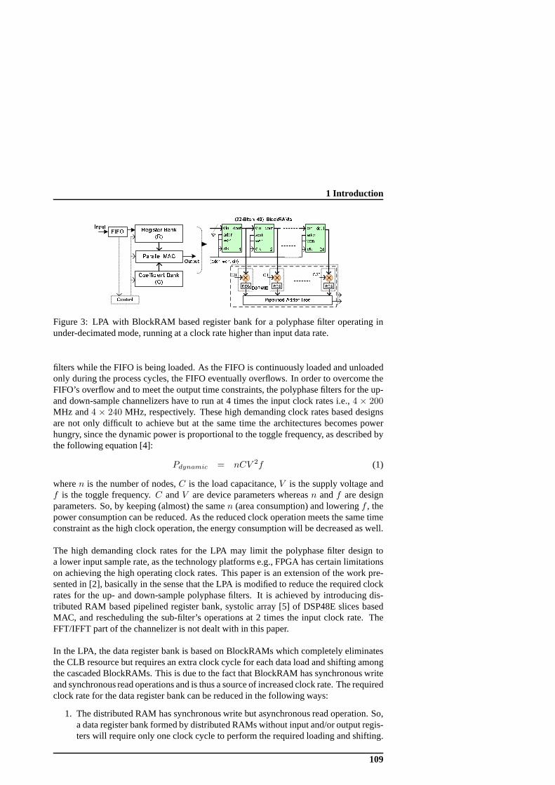
1 Introduction
�������� ���
������ ���
��
��������� ���
���
�������
����
��� ��
!� ��
"# $%%&
%'()%*+
,-.
/0+
123456�7 8 9:; 5��<=>?@7
$%%&
%'()%*+
,-.
/0+
A$%%&B /0+B ,-.C
D #
E6 F�6�FG ?GGF� H�FF
IJKLMN
OP OD O#"
$%%&
%'()%*+
,-.
/0+
#L
QRS QRS QRS
Figure 3: LPA with BlockRAM based register bank for a polyphase filter operating inunder-decimated mode, running at a clock rate higher than input data rate.
filters while the FIFO is being loaded. As the FIFO is continuously loaded and unloadedonly during the process cycles, the FIFO eventually overflows. In order to overcome theFIFO’s overflow and to meet the output time constraints, the polyphase filters for the up-and down-sample channelizers have to run at 4 times the inputclock rates i.e.,4 × 200MHz and4 × 240 MHz, respectively. These high demanding clock rates based designsare not only difficult to achieve but at the same time the architectures becomes powerhungry, since the dynamic power is proportional to the toggle frequency, as described bythe following equation [4]:
Pdynamic = nCV 2f (1)
wheren is the number of nodes,C is the load capacitance,V is the supply voltage andf is the toggle frequency.C andV are device parameters whereasn andf are designparameters. So, by keeping (almost) the samen (area consumption) and loweringf , thepower consumption can be reduced. As the reduced clock operation meets the same timeconstraint as the high clock operation, the energy consumption will be decreased as well.
The high demanding clock rates for the LPA may limit the polyphase filter design toa lower input sample rate, as the technology platforms e.g.,FPGA has certain limitationson achieving the high operating clock rates. This paper is anextension of the work pre-sented in [2], basically in the sense that the LPA is modified to reduce the required clockrates for the up- and down-sample polyphase filters. It is achieved by introducing dis-tributed RAM based pipelined register bank, systolic array[5] of DSP48E slices basedMAC, and rescheduling the sub-filter’s operations at 2 timesthe input clock rate. TheFFT/IFFT part of the channelizer is not dealt with in this paper.
In the LPA, the data register bank is based on BlockRAMs whichcompletely eliminatesthe CLB resource but requires an extra clock cycle for each data load and shifting amongthe cascaded BlockRAMs. This is due to the fact that BlockRAMhas synchronous writeand synchronous read operations and is thus a source of increased clock rate. The requiredclock rate for the data register bank can be reduced in the following ways:
1. The distributed RAM has synchronous write but asynchronous read operation. So,a data register bank formed by distributed RAMs without input and/or output regis-ters will require only one clock cycle to perform the required loading and shifting.
109

Paper C
It therefore results in an overall reduced clock rate demand, but requires extendedCLB resources. The required operating clock rate for the LPAfor the up- anddown-sample polyphase filters with distributed RAM based register bank reducesto 3x the input data rates.
2. In the LPA with distributed RAM based register bank, the scheduling of the loadand process cycles can also be improved to further reduce therequired operatingclock rates. The idea is to start the processing of the sub-filters (process-cycle)while data is loading from the FIFO (load-cycle), instead ofwaiting for the com-plete loading of the data-loaded (targeted) sub-filters before processing. In thiscase, the process-cycle continues for M sub-filters, but thedata loading is stoppedfor non data-loaded (non-targeted) sub-filters.
���������� ������� ���������� �������
����������
�������
����������
�������
��� ������
��� ������
�������� �
�������
�������� �
�������
���
���
Figure 4: Scheduling of load and process cycles for (a) LPA and (b) interlaced LPA
This is the only time when input data is pushed onto the FIFO without being pulledat the same time. Since the number of non-targeted sub-filters is less than the num-ber of targeted sub-filters, the FIFO does not grow as rapidlyas in the previous casewhere process-cycle starts after completing the load-cycle as shown in Fig. 4a. Thisinterlaced scheme for loading and processing as shown in Fig. 4b reduces the over-all clock cycles count and therefore reduces the required clock rate. By operatingthe sub-filter’s processes at 2x clock, the FIFO growth in the(extended) processcycle gets undone in the next couple of sub-filter’s processing within the next loadcycle. So, the required operating clock rates for up- and down-sample polyphasefilter reduces to 2x still meeting the output timing constraints.
3. In interlaced LPA, most of the process cycles which are overlapped by the loadcycles are idling as they are waiting for the next available data from the input FIFO.To make efficient use of these idling cycles of 2x clock, an RA is introduced wherenon-targeted sub-filter’s processing is achieved by idlingcycles of 2x clock insteadof processing them after the load cycle. By doing so, the length of the process cyclebecomes equal to the length of the load cycle which will also eliminate the need forthe input FIFO.
The RA, operating at twice as high a data clock rate, processes the input data whilesimultaneously loading to the sub-filters on the first cycle of the 2x clock and the nextcycle of the 2x clock get used to process the non-targeted sub-filter. By using this schemethe non-targeted sub-filters get processed within the time frame of the targeted sub-filtersand therefore reduce the overheads as in the case of LPA and interlaced LPA.
110

2 RA Scheduler
2 RA Scheduler
Now we present the RA scheduling for the up- and down-sample polyphase filters for thechannelizers shown in Fig. 1 and Fig. 2. On the RA for the down-sample polyphase filter,operating at 2x process clock, the 24 input data periods have48 periods of 2x clocks.It schedules the non-targeted sub-filter’s(R39, R38, ..., R24) processing by interlacingit with the targeted sub-filter’s(R23, R22, ..., R0) processing during the first state, asshown in Fig. 5. It will be extended accordingly for the 5 periodic states of the polyphaseengine. As there are 16 non-targeted sub-filters in each state, the rest of the 8 time slotsof the 2x clock allocated for the non-targeted sub-filter’s processing remain unused, andwe call them invalid sub-filters. The sliding data loading for the 5 periodic states need48×5 = 240 distinct addresses for the data address pointer. As the sliding loading of datainteracts with the cyclic shifted set of coefficients, the coefficient address pointer needsthe same sized distinct addresses as the data address pointer. The unused time slots for thenon-targeted sub-filter processing (invalid sub-filter) are addressed by zero-valued dataand coefficients at address 40. Because of the interlaced processing of the non-targetedsub-filters with the targeted sub-filters, the final processed outputs need reordering tobring them in their normal order, and delivering them at the required output rate.
��
���
���
��
���
���
����� ��� �
����� ���
��������� ������� ���� �������� �� ! ����� �
"#
$"
%&'
()��)�
*+� *+�� *+�� *+,-
./0.1
23# 234 23$ 536
.78
53"9 53": 53"; 53<#53"=
�)�>������
����?���
*+�
.@/
*A*BCDEFGCGH IJKBLMNCGEI
O3# O34 O3$6
P6; .@@ P6:
O3$< O3"=
./Q
53<4
R3# R34 R3$ R36 R36; R3"#
���
S �)�
���
'�!
TU TU TU
�)�>������
V����W6; W$$ W6: W# XYZ W6; W$$ W# XYZ
�[ '�!
�\]^DCD _ADH �
`a^DCD _ADH
�)�>������
b c� d �� e
R3"4 R3"$
f*gDNMH IJKBLMNCGE
W"# W6:
#
P"# P"# P4< P4"
#
P"# P"#
W$6 W$6
#O3$"#
c� d ��
�)�>������
V����?���
W"#
*+�,
NDCG*hi
W"# W"#
6;
�, NADHIj ,� kEAhGII l m MHNG �, NADHIj ,� kEAhGII l m MHNG
$$ 6: "# 4< 6: 4" 49$6 "## 6; "# "#
6; $$ 6:$6 #"# "# 6; $$ 6:$6 #"# "#
Figure 5: Scheduling of the first two states for RA for the down-sampling polyphase filter.The time-lag for processing non-targeted sub-filters is overcome by using 2x clock andprocessing non-targeted sub-filters along with targeted sub-filters.
111
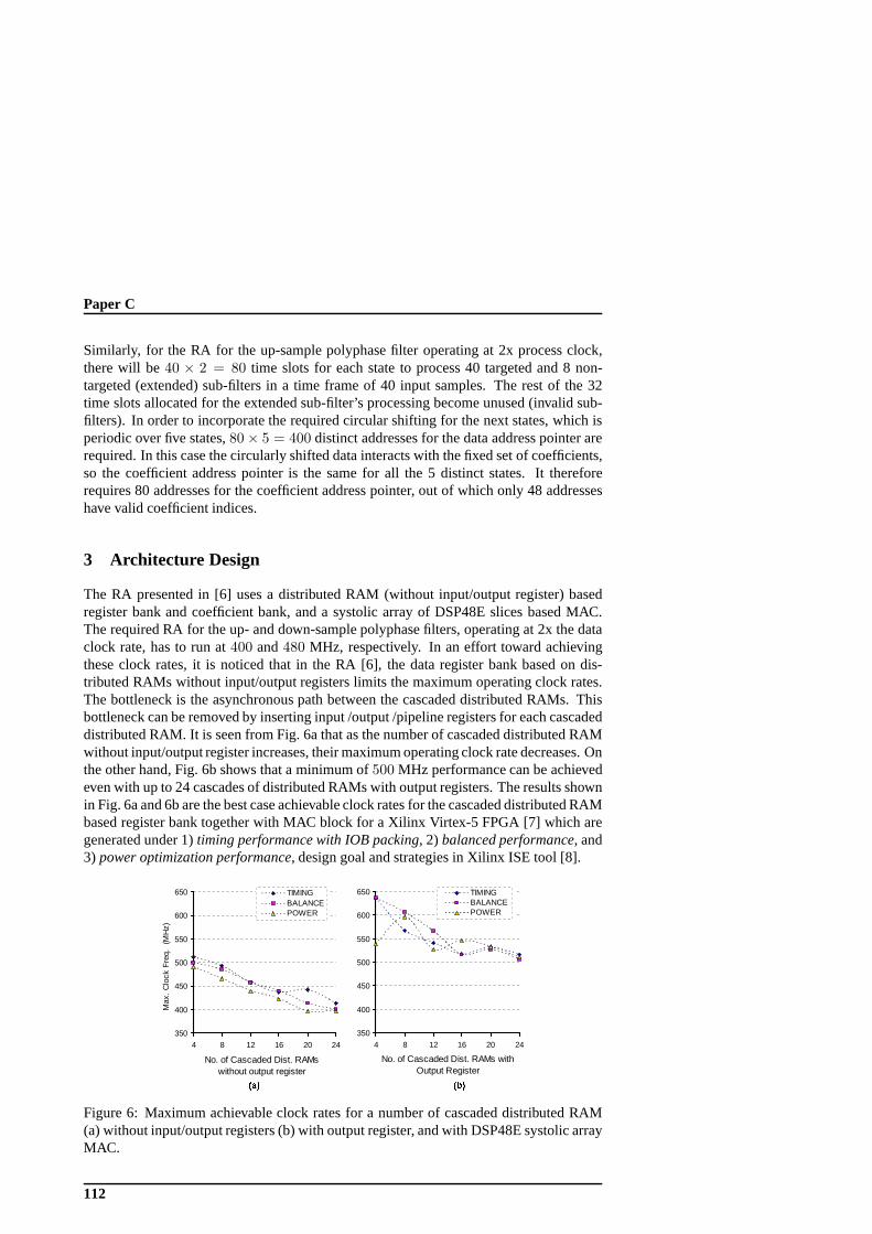
Paper C
Similarly, for the RA for the up-sample polyphase filter operating at 2x process clock,there will be40 × 2 = 80 time slots for each state to process 40 targeted and 8 non-targeted (extended) sub-filters in a time frame of 40 input samples. The rest of the 32time slots allocated for the extended sub-filter’s processing become unused (invalid sub-filters). In order to incorporate the required circular shifting for the next states, which isperiodic over five states,80× 5 = 400 distinct addresses for the data address pointer arerequired. In this case the circularly shifted data interacts with the fixed set of coefficients,so the coefficient address pointer is the same for all the 5 distinct states. It thereforerequires 80 addresses for the coefficient address pointer, out of which only 48 addresseshave valid coefficient indices.
3 Architecture Design
The RA presented in [6] uses a distributed RAM (without input/output register) basedregister bank and coefficient bank, and a systolic array of DSP48E slices based MAC.The required RA for the up- and down-sample polyphase filters, operating at 2x the dataclock rate, has to run at400 and480 MHz, respectively. In an effort toward achievingthese clock rates, it is noticed that in the RA [6], the data register bank based on dis-tributed RAMs without input/output registers limits the maximum operating clock rates.The bottleneck is the asynchronous path between the cascaded distributed RAMs. Thisbottleneck can be removed by inserting input /output /pipeline registers for each cascadeddistributed RAM. It is seen from Fig. 6a that as the number of cascaded distributed RAMwithout input/output register increases, their maximum operating clock rate decreases. Onthe other hand, Fig. 6b shows that a minimum of500 MHz performance can be achievedeven with up to 24 cascades of distributed RAMs with output registers. The results shownin Fig. 6a and 6b are the best case achievable clock rates for the cascaded distributed RAMbased register bank together with MAC block for a Xilinx Virtex-5 FPGA [7] which aregenerated under 1)timing performance with IOB packing, 2) balanced performance, and3) power optimization performance, design goal and strategies in Xilinx ISE tool [8].
350
400
450
500
550
600
650
4 8 12 16 20 24
No. of Cascaded Dist. RAMs without output register
Max
. C
lock
Fre
q.
(MH
z)
TIMINGBALANCEPOWER
350
400
450
500
550
600
650
4 8 12 16 20 24
No. of Cascaded Dist. RAMs with Output Register
Max
. C
lock
Fre
q.
(MH
z)
TIMINGBALANCEPOWER
��� ���
Figure 6: Maximum achievable clock rates for a number of cascaded distributed RAM(a) without input/output registers (b) with output register, and with DSP48E systolic arrayMAC.
112
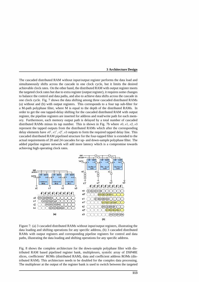
3 Architecture Design
The cascaded distributed RAM without input/output register performs the data load andsimultaneously shifts across the cascade in one clock cycle, but it limits the desiredachievable clock rates. On the other hand, the distributed RAM with output register meetsthe targeted clock rates but due to extra register (output register), it requires some changesto balance the control and data paths, and also to achieve data shifts across the cascade inone clock cycle. Fig. 7 shows the data shifting among three cascaded distributed RAMs(a) without and (b) with output registers. This correspondsto a four tap sub-filter fora M-path polyphase filter, where M is equal to the depth of the distributed RAMs. Inorder to get the one tapped-delay shifting for the cascaded distributed RAM with outputregister, the pipeline registers are inserted for address and read/write path for each mem-ory. Furthermore, each memory output path is delayed by a total number of cascadeddistributed RAMs minus its tap number. This is shown in Fig. 7b wheres0, s1, s2, s3represent the tapped outputs from the distributed RAMs which after the correspondingdelay elements haves0′, s1′, s2′, s3 outputs to form the required tapped delay line. Thiscascaded distributed RAM pipelined structure for the four-tapped filter is extended to theactual requirements of 20 and 24 cascades for up- and down-sample polyphase filter. Theadded pipeline register network will add more latency whichis a compromise towardsachieving high operating clock rates.
���
���
��
��
��
��
��
��
��
�� � �� ��
�� � �� ��
�� � �� ��
�� � �� ��
�� � �� ��
�� � �� ��
�� � �� ��
����
������
��
��
��
��
�� �� �� ��
�� � �� ��
�� � �� ��
�� � �� ��
�� � �� ��
��������������
!
"# $%%#
&'(
��������������
!
"# $%%#
&'(
��������������
!
"# $%%#
&'(
����
��������������
!
"# $%%#
&'(
��������������
!
"# $%%#
&'(
��������������
!
"# $%%#
&'(
������
�� �� ��
�� �� ��
��
Figure 7: (a) 3 cascaded distributed RAMs without input/output registers, illustrating thedata loading and shifting operations for any specific address, (b) 3 cascaded distributedRAMs with output registers and corresponding pipeline registers for control and datapaths, illustrating the data loading and shifting operations for any specific address.
Fig. 8 shows the complete architecture for the down-sample polyphase filter with dis-tributed RAM based pipelined register bank, multiplexers,systolic array of DSP48Eslices, coefficients’ ROMs (distributed RAM), data and coefficient address ROMs (dis-tributed RAM). This architecture needs to be doubled for thecomplex data processing.The multiplexer at the output of the register bank is used to switch between the targeted
113

Paper C
and non-targeted sub-filter’s processing. The parallel data from the multiplexer block isdelayed element-by-element to time align the sub-filter’s MAC process in the systolic ar-ray of DSP48E slices. The coefficients from the respective coefficient memories beingdriven by the same address pointer need the same element-by-element delay as the datafrom the register bank, to time align the coefficients with their corresponding data. Thisrequired delay for the coefficients is achieved efficiently by an offset address filling ofthe coefficient memories instead of using extra delay registers as required by the datapath. The coefficient memories are shared by both the real andimaginary data processingunit. The first data input takes 25 clock cycles (24 clock cycles for the tap-0 delays and1 clock cycle for the multiplexer) to be available for the MACblock which needs to besynchronized to its corresponding coefficient set. This synchronization is achieved by anequivalent advanced count operation in the coefficient address counter. The RA for theup-sample polyphase filter is the same as the down-sample polyphase filter but it has acascade of 20 distributed RAMs instead of 24, for its register bank, and correspondingcoefficient bank and addressing memories.
����� ���
�� ���� ���
����
��������
����
����� ��� ����
����
!�"#�
$%&�
�''�
(�
)*
+,-..,
/01
����� ���
�� ���� ���
)*
+,-..,
/01
����� ���
�� ���� ���
)*
+,-..,
/0123
����� �4�
56 ���� ���
789:: 6 789:: 5
����� �4�
� ���� 5�6�
789::;<==>
?�@<>A B8C@�9>
6 5DE�
789::;7@�>
FG�HH�I����
����
789:: � 789:: 5D
����� �4�
� ���� 5�6�
=<�<;<==>
?�@<>A B8C@�9>
6 5DE�
=<�<;7@�>
����
! ��
����
! ��
����� �4�
56 ���� ���
����� �4�
56 ���� ���
����� �4�
56 ���� ���
JKLM
JKLN
JKLL
JKO
JKL
JKO
JKLN
6
�PQ��R
JKO
JKO
JKO
JKO
JKO
JKO
JKO
JKO
JKO
JKO
JKO
JKO
S���G��I
T����
Figure 8: The complete architecture for the down-sample polyphase filter with 24 cas-caded distributed RAMs, delay/pipeline registers, multiplexers, systolic array of DSP48Eslices, coefficients’ distributed-ROMs, data and coefficient address counters, and dataaddress and coefficient address distributed ROMs.
114

4 Results
4 Results
The presented RA for the up- and down-sampling polyphase filters are mapped to a Xil-inx Virtex-5 (xc5vsx50t-3ff1136) FPGA in the form of I-Q components. The resourceusage of the real FPGA implementation for these architectures in terms of (a) slice reg-isters, slice LUTs, and slice LUT flip-flop pairs, and (b) dedicated resources is presentedin Fig. 9a and Fig. 9b, respectively. These results are generated under thetiming per-formance with IOB packingdesign goal and strategy, and withnon-resource sharingandauto LUT combiningoptions in Xilinx ISE tool. The resource usage for the slice registersand slice LUTs presented in Fig. 9a is on an average of 3.2 times higher as compared tothe usage presented in [2] for their LPA counter parts. This is due to the fact that the RAuses distributed RAM based data and coefficient banks, and added pipeline registers tomeet the timing constraints up to480 MHz. A power consumption analysis focusing onthe dynamic power is performed for the RA for the up- and down-sample polyphase filtersby using the Xilinx XPA tool [8]. The activity rates based on the input test vectors are cal-culated by running ModelSim [9] post place and route simulations for a run length of 500µs. The corresponding thermal settings for these power analyses are 50 degrees Celsiusas ambient temperature with 250 LFM air flow and medium profileheat sink. The togglerates for the flip-flop, I/O and DSP, and the corresponding power consumptions by the up-and down-sample polyphase filters are shown in Fig. 9c and Fig. 9d, respectively. Thedynamic power consumptions of 1.9 and 2.6 Watts correspond to the 2x operating clockrates i.e., 400 and 480 MHz for the up- and down-sample polyphase filters, respectively.
0
1000
2000
3000
4000
5000
Down-sample Polyphase Filter
Up-sample Polyphase Filter
Slice RegistersSlice LUTsSlice LUT Flip-Flop Pairs
0
0.5
1
1.5
2
2.5
3
Down-samplePolyphase Filter
Up-sample Polyphase Filter
Wat
ts (
W)
Leakage Power
Dynamic Power
0
10
20
30
40
50
60
Down-sample Polyphase Filter
Up-sample Polyphase Filter
No.
of
Res
ourc
es
DSP48E
0
10
20
30
40
50
60
70
80
Down-samplePolyphase Filter
Up-sample Polyphase Filter
Tog
gle
Rat
e (%
)
Flip-FlopI/O DSP
��� ���
��� ���
Figure 9: Resource usage in terms of (a) slice registers, slice LUTS, and slice LUT flip-flop pairs (b) dedicated resources for Xilinx Virtex-5 FPGA,(c) toggle rates for the flip-flops, I/Os and DSP, and (d) corresponding power consumption(dynamic and leakage)for the down- and up-sample polyphase filters, respectively.
115

Paper C
5 Conclusion
We have presented and demonstrated the RA for the serial polyphase structure with paral-lel MAC for the up- and down-sampling polyphase filters operating in an under-decimatedscenario. In terms of the targeted design goals of Time and Power optimizations, the RA,in contrast to its LPA counterpart, operates at 2x clock rateand efficiently schedules andprocess the sub-filters within the data load time. The run-time scheduling schemes for em-bedding the required sliding and cyclic shifting for the up-and down-sampling polyphasefilters are presented. The data register bank based on distributed RAMs is modified byinserting pipeline and corresponding balancing registersto achieve the targeted operatingclock rates up to 480 MHz on the Xilinx Virtex-5 FPGA. The FPGAresource usage andpower consumption analysis is presented. The RA at 2x operating clock rate being theminimum possible rate for the serial polyphase structure with parallel MAC operating inan under-decimated scenario turns out to be a preferable choice for the time and powerefficient solution for its FPGA based architectures.
References
[1] fred harris, Chris Dick, ”Polyphase Channelizer Performs Sample Rate Change Re-quired for both Matched Filtering and Channel Frequency Spacing”, in 43rd AsilomarConference on Signals, Systems and Computers, Pacific Grove, CA, 2009.
[2] Mehmood Awan et al., ”FPGA Implementation Analysis of Polyphase ChannelizerPerforms Sample Rate Change Required for both Matched Filtering and Channel Fre-quency Spacing”, in44th Asilomar Conference on Signals, Systems and Computers,Pacific Grove, CA, 2010.
[3] Xilinx UG193 (v3.3), ”Virtex-5 FPGA XtremeDSP Design Considerations UserGuide”, Jan 12, 2009.
[4] Abusaidi, Peggy et al., ”Virtex-5 FPGA System Power Design Considerations”, Xil-inx WP285 (V1.0), Feb 14, 2008.
[5] H.T. Kung, ”Why Systolic Architectures?”,IEEE Computer, vol. 15, no. 1, pp 37-46,Jan, 1982.
[6] Mehmood Awan et al., ”Hardware Architecture Analysis ofPolyphase Filter BanksPerforming Embedded Resampling for Software Defined Radio Front-Ends”,100Gand Beyond: Trends in Ultrahigh-Speed Communications (Part I), ZTE Communica-tions, Vol. 10, No. 1, pp. 54-62, Mar 2012. ISSN 1673-5188
[7] UG190 (v5.3), ”Virtex-5 FPGA User Guide”, May 17, 2010.
[8] Xilinx ISE 10.1 Design Suite Software Manuals and Help, 2008.
[9] ModelSim SE User’s Manual, Software Version 6.5, 2009.
116

Paper D
FPGA Implementation Analysis of Polyphase ChannelizerPerforming Sample Rate Change Required for both Matched
Filtering and Channel Frequency Spacing
Mehmood Awan, Peter Koch, Chris Dick, and fred harris
This paper was published in:44th Asilomar Conference on Signals, Systems, and Computers

Copyright c©IEEE 2010The layout has been revised

1 Introduction
Abstract
The paper presents the architectural domain analysis for FPGA (Field ProgrammableGate Array) implementation of a polyphase filter bank channelizer with an embed-ded square root shaping filter in its polyphase engine that performs two differentre-sampling tasks required for spectral shaping and for M-channel channelizer. Interms of algorithms; Radix-2 FFT, Prime Factor and WinogradFourier Transform areconsidered for IFFT, where as the polyphase filter is analyzed in terms of symmetricstructure, and serial polyphase structures with serial andparallel MAC approaches.The computational workload for these algorithms and their implementation structuresare presented together with their hardware mapping to a Virtex-5 FPGA by exploitingthe inherent parallelism. Their resource utilizations andDesign Space Exploration interms of Area-Time is presented along with different optimization techniques.
1 Introduction
Traditional polyphase filter bank are formed from three building blocks, an M-port com-mutator, an M-path polyphase partition of a prototype low-pass filter and an M-pointIFFT. These blocks can be arranged to perform M-channel channelizer for modulator(where up to M input time series form an output time series composed of M-equallyspaced frequency division multiplexed (FDM) channels) anddemodulator (where up toM-equally spaced frequency division multiplexed (FDM) channels are converted to M-interlaced time division multiplexed (TDM) channels). These up-converter and down-converter, based on maximally decimated filter banks, are dual graph which by virtue oftheir linear time varying structures perform the opposite tasks of up-sample and down-sample channelization [1]. There are a number of different scenarios where we want thatthe different up-sampling and down-sampling tasks be performed in the channelizationprocess (non-maximally decimated system). Polyphase filter banks performing dual sam-ple rate change both for up-sample and down-sample channelization are presented in [1]where a system has 32 channels separated by 6MHz center frequencies and each havinga 5MHz symbol rate shaped by square root Nyquist filter with 20% excess bandwidth.Figures 1 and 2 show the down-sample and up-sample channelizers.
0 0
1 1
2 2
3 3
23
312430
39
40 4040
........
........
…
36
39
38
37
0
.................
40
-Pa
th P
oly
ph
ase
Filt
er
40
-Po
int
IFFT
fs=6*40 MHz= 240 MHz
f =fs/40
=240/40=6 MHz
channel
f =
=240/24=10 MHz=2 f
out fs/24
symbol
FDM
TDM
Circ
ula
r In
pu
t B
uff
er
Circ
ula
r O
utp
ut
Bu
ffe
r
State Engine
Figure 1: 40-Path Polyphase FDM-to TDM Channelizer with 24-to-1 Down-Sampling [1].
119
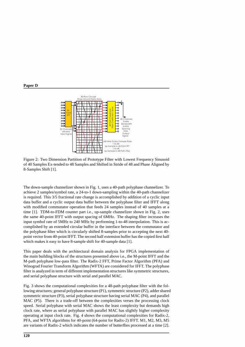
Paper D
40PointIFFT
48-P
ath
Po
lyp
ha
seFilt
er
Co
eff
icie
nt
Ba
nk
80 Row CircularWrap-Around Data Array
32 Channelsof5-MHz
Input Signal
40 Channels:5-MHz
Bandwidth6-MHz
SpacingFDM
OutputSignal
240 MHz Output Sample Rate:1-to-40
Up-Sample in 40-Point FFT1-to-48
Up-Sample in 48-Path Filter
Figure 2: Two Dimension Partition of Prototype Filter with Lowest Frequency Sinusoidof 40 Samples Ex-tended to 48 Samples and Shifted in Stride of48 and Phase Aligned by8-Samples Shift [1].
The down-sample channelizer shown in Fig. 1, uses a 40-path polyphase channelizer. Toachieve 2 samples/symbol rate, a 24-to-1 down-sampling within the 40-path channelizeris required. This 3/5 fractional rate change is accomplished by addition of a cyclic inputdata buffer and a cyclic output data buffer between the polyphase filter and IFFT alongwith modified commutator operation that feeds 24 samples instead of 40 samples at atime [1]. TDM-to-FDM counter part i.e., up-sample channelizer shown in Fig. 2, usesthe same 40-point IFFT with output spacing of 6MHz. The shaping filter increases theinput symbol rate of 5MHz to 240 MHz by performing 1-to-48 interpolation. This is ac-complished by an extended circular buffer in the interface between the commutator andthe polyphase filter which is circularly shifted 8-samples prior to accepting the next 40-point vector from 40-point IFFT. The second half extension buffer has the copied first halfwhich makes it easy to have 8-sample shift for 40-sample data[1].
This paper deals with the architectural domain analysis forFPGA implementation ofthe main building blocks of the structures presented above i.e., the M-point IFFT and theM-path polyphase low-pass filter. The Radix-2 FFT, Prime Factor Algorithm (PFA) andWinograd Fourier Transform Algorithm (WFTA) are considered for IFFT. The polyphasefilter is analyzed in term of different implementation structures like symmetric structures,and serial polyphase structure with serial and parallel MAC.
Fig. 3 shows the computational complexities for a 48-path polyphase filter with the fol-lowing structures; general polyphase structure (P1), symmetric structure (P2), adder sharedsymmetric structure (P3), serial polyphase structure having serial MAC (P4), and parallelMAC (P5). There is a trade-off between the complexities verses the processing clockspeed. Serial polyphase with serial MAC shows the least complexity but demands highclock rate, where as serial polyphase with parallel MAC has slightly higher complexityoperating at input clock rate. Fig. 4 shows the computational complexities for Radix-2,PFA, and WFTA algorithms for 40-point (64-point for Radix-2) IFFT. M1, M2, M3, M5are variants of Radix-2 which indicates the number of butterflies processed at a time [2].
120

1 Introduction
P1 P2 P3 P4 P50
500
1000
1500
2000
MultsAddsRegs
Figure 3: Complexity analysis for 48-path polyphase filter;general polyphase structure(P1), symmetric structure (P2), adder shared symmetric structure (P3), serial polyphasestructure having serial MAC (P4), and parallel MAC (P5).
M1 M2 M3 M5 PFA WFTA0
500
1000
1500
Multsadds
Figure 4: Complexity analysis for 40-point IFFT with Radix-2, Prime factor and Wino-grad Fourier Transform Algorithms. M1, M2, M3, M5 are variants of Radix-2 FFT.
The WFTA algorithm is the most efficient having only 100 real multiplications for 40-point IFFT.
Based on the computational complexity analysis, the WFTA algorithm and the serialpolyphase structures are selected for the mapping to the target platform Virtex-5 (xc5vsx50t-3ff1136). Fixed point analysis is performed to determine the bit widths keeping the quan-tization errors below 60dB (normally required). The downsample polyphase channelizerhas 40 paths filter with 24 taps each. A straight forward mapping of this structure toFPGA where all the filter coefficients and tapped delay lines are CLB slice register based,results in a resource utilization which is more than the slice registers and LUTs on thetarget platform Virtex-5. It requires various resource optimal techniques to map thesestructures, both by optimizing the algorithmic structuresand by using the dedicated re-sources within the FPGA. The filter coefficient bank can easily be replaced by FPGABlockRAMs to optimize the resources, but the critical portion is polyphase partitioneddata bank (register bank), especially when we have to perform the embedded resamplingwithin that. In case of a maximally decimated system, where the downsampling factoris equal to polyphase partition, FIFOs can be used as delay lines to have the most opti-mal structure, as described in [3]. But for non-maximally decimated system which wehave in this scenario, a two dimensional RAM based solution is needed. Fig. 5 shows theresource utilization for mapping 24×40 register bank (16-bit) by considering differentoptions available on the Virtex-5 FPGA.
121

Paper D
0
5000
10000
15000
Slice RegSlice LUTs
SliceRegisters& LUTs(Real)
DistributedMemory Cell(16−bit)(Real)
40x32−bitDistributedMemory(Complex)
40x32−bitBlockRAM(Complex)
Figure 5: 20×40 Register Bank Resource Utilizations by using Slice Registers and LUTs,Distributed Memory, and BlockRAMs.
The 24×40 register bank based on slice registers and LUTs results in[53, 26]% utilizationfor slice registers and LUTs respectively. It’s only for real data and therefore the num-bers would be double for the complex data. Next, each data register in the sub-filters isreplaced by a distributed memory based memory cell (16-bit)and the resource utilization(for real data only) comes out to be [0, 24]% for slice registers and LUTs respectively. Itsaved the slice registers but the LUTs ultilization is almost the same as before. In Virtex-5, each CLB has 64-bit distributed RAM [4], but it is bit-addressable, so for 16-bit data,16 CLBs are collectively used as a single 16-bit register. The rest of the 63 bits in eachCLB remained unused. Based on this analysis, distributed memory is used such that each64-bit memory contribute 1-bit to 16-bit data element for 64sub-filters (only 40 are used).So here comes the effectiveness that the memory which was previously used for only onesub-filter is now being used for all the 40 sub-filters. The bit-width is further extendedto 32-bit to incorporate complex data (16 + 16 bits) and the resource utilization dramati-cally decrease to 2% (for complex data). It will also eliminate the need for multiplexersto select the desired sub-filter’s data elements for the caseof shift register based registerbank. The same concept is further applied to BlockRAMs whichcompletely eliminatethe CLBs ultilization. The BlockRAMs utilization for (40×32-bit) register bank is 12BlockRAMs, which corresponds to 9% utilization for Virtex-5.
In order to use BlockRAMs based register banks, we have to payan extra clock cyclefor each data load and shift. The reason is that as 24 memories(40×32-bit) are cas-caded to form 24×40 register bank and the data shift in the sub-filters requires data tobe available from the preceding memory. So it requires one clock cycle to read the dataelement and then the next clock will load the new data elementalong with shifting ofthe sub-filter, as shown in Fig. 6. According to the polyphasechannelizer configurationsin [1], the downsampling polyphase filter loads 24 data elements and process 40 sub-filters, whereas the upsampling polyphase filter loads 40 data elements and process 48sub-filters, so the run time processing at the input sample rate fs for serial polyphasestructure with parallel MAC andN/M times thefs for serial polyphase structure withserial MAC is not possible. Therefore, the polyphase engineis run at higher clock speedsand a FIFO is used to interface with the input data at lower rate. So a ”load and process”
122

1 Introduction
�� �� ����
�� ���
���
� �
���
���
�� � ���� �
�������
���
���
� �
���
���
���
���
� �
���
���
�� ��
���
���
���
� � �
�� � ���� �
�������
�� � ���� �
�������
Figure 6: 40×32-bit memory cascade to form 24×40 register bank. One clock cycleto load the date form the memories and another clock cycle to shift the data throughmemories.
architecture is required where during load, data elements are fed from the input FIFOto sub-filters as directed by the data-pointer to embed the required shift. In the processphase, coefficient-pointer and data-pointer having embedded shifts select the coefficientand data memory elements to perform MAC operations. The loadand process sequencesfor the downsampling polyphase filter which has 4 distinct states, both for its parallel andserial MAC architecture, is presented in Table 1:
Load Process
Load 24 Data Elements Process 40 Sub-filters
Data Loading Data Address Sequence: [0]Address Sequence: Coefficient Address Sequence:[23, 39, 15, 31, 7] [0, 24, 32, 16] (Parallel MAC)
[0, 24, 32, 16]×24 (Serial MAC)
Table 1: Load & Process sequences for downsampling polyphase filter
In the upsampling polyphase filter, the 40-point IFFT outputis extended to 80-pointsand loaded to a 20×80 register bank, and after circular shifting of 8 samples instrideof 48, only a 20×48 register bank is used for filter processing. This apparently seemsto be quite complicated and resource demanding as we are extending the register bank.But by employing a clever address scheme, we can do with only a20×40 register bankto perform the required circular shift. It has been noticed that each column in the regis-
123

Paper D
ter bank which is (40×32-bit) BlockRAM has a circular shift of multiples of 8 modulo40. So instead of the common address bus, if each memory has a separate address buswith its own data-pointer having the offset of multiples of 8modulo 40 from the adjacentmemories, we can achieve the required circular shift. The last 8 sub-filters have the samedata (or more precisely same data-pointer) as the first 8 sub-filter have, only coefficientpointers are different. It is further noticed that data pointers having offset of multiples of8 modulo 40 results in 5 distinct pointers which are repeatedover for 20 columns. Theregister bank based on (40×32-bit) BlockRAMs for the upsampling polyphase filter withseparated data pointers is shown in Fig. 7. The load and process sequences for the up-
����� ����� �����
�� �� ��
�� ���
����
���
���
���
�� � ������
����� !"
���
����
���
���
���
���
����
���
���
���
�� � ������
����� !"
�� � ������
����� !"
������
# $ $%
Figure 7: 40×32-bit memory cascade to form 48×20 register bank. It uses separateaddress buses for each memory block to embed the required circular shift.
sampling polyphase filter, both for its parallel and serial MAC architecture is presented inTable 2.
Load Process
Load 40 Data Elements Process 48 Sub-filters
Data Loading Data-pointer is modulo-40, so theAddress: [0] last 8 sub-filters take the same
data as first 8 sub-filters
5 distinct Data-pointer:[0, 8, 16, 24, 32] Modulo 40
Coefficient-pointer:[0] Parallel & Serial MACs
Table 2: Load & Process sequences for upsampling polyphase filter
The filter coefficient bank is mapped on to ROMs by using BlockRAMs resources, bothfor parallel and serial MAC architecture. For the parallel structure, each column in thecoefficient bank corresponds to a separate ROM, whereas the serial MAC structure usesa single large ROM. The final resource utilization for the downsampling and upsamplingpolyphase filters based on the serial polyphase structure with parallel and serial MAC is
124

1 Introduction
0
200
400
600
800
1000
1200
1400
Parallel Design Serial Design Parallel Design Serial Design
Down-sampling polyphase filter
Up-sampling Polyphase Filter
Slice Registers
Slice LUTs
BlockRAM
DSP48Es
Figure 8: Resource Utilization (in terms of Slice Registers, Slice LUTs, BlockRAMsand DSP48e) for the upsampling and downsampling polyphase filters for their serialpolyphase architectures with parallel and serial MACs.
presented in Fig. 8. The downsampling polyphase filter utilizes 3% of CLBs, 18% ofBlockRAMs and 16% of DSP48e slices for its parallel structure where as the serial struc-ture utilizes 1% of CLBs, 9% of BlockRAMs and 0% of DSP48e slices. The resourceutilization for the upsampling polyphase filter is almost the same as for downsamplingpolyphase filter. It uses the same architecture with different data and coefficient pointersequences. These resource utilizations can also be analyzed in comparison to their pro-cessing time in term of clock cycles. Fig. 9 shows the DSE (Design Space Exploration)graph in terms of Area and Time. The smaller the processing Time, the larger is the re-quired Area (parallel design) and the smaller the Area, the larger is the processing Time(serial design). The downsampling polyphase filter with parallel structure requires 99clock cycles for 40 outputs from 24 data inputs, whereas the serial structure requires1015 clock cycles for the same outputs. Similarly, the upsampling polyphase filter withparallel structure requires 138 clock cycles for 48 outputsfrom 40 data inputs, whereasthe serial structure requires 1044 clock cycles for the sameoutputs. All the designs canoperate at a maximum clock speed of 225 MHz.
DSE (Area-Time Graph)
0
200
400
600
800
1000
1200
1400
0 200 400 600 800 1000 1200
Time (No- of Clock Cycles)
Are
a (N
o. o
f L
UT
s)
Rx Parallel design
Rx Serial Design
Tx Parallel Design
Tx Serial Design
Figure 9: Design Space Exploration (Area-Time) for the downsampling and upsamplingpolyphase filter for their serial polyphase architectures with parallel and serial MACs.
125

Paper D
According to the complexity analysis for 40-point IFFT presented in Fig. 4, WinogradFourier Transform Algorithm has the lowest computational complexity because of elim-ination of twiddle factors and complex multipliers. The 40-point Winograd transform iscarried out as 5x8 transform (5 and 8 are relative prime numbers). The 40-point vector isloaded to a 5x8 matrix by Chinese Remainder Theorem. The 5-point transform is carriedout 8 times and then on intermediate outputs, 8-point transform is carried out 5 times andfinally data is unloaded by Ruritanian mapping. So there are two building blocks, i.e., a5-point transform and a 8-point transform. The 5-point Winograd transform requires 10multipliers and 34 adders, whereas the 8-point transform requires 4 multipliers and 52adders. These algorithms can be scheduled in a number of different ways depending onallocated processing resources in terms of adders and multipliers.
For instance, in design no. 1, by allocating 10 multipliers and 8 adders for the 5-pointtransform, it takes 6 clock cycles to process. Similarly, byallocating 4 multipliers and 16adders for the 8-point transform, it takes 5 clock cycles to process. So, for the 40-pointtransform, 6 clock cycles x 8 times and 5 clock cycles x 5 times; total 48 + 25 = 73clock cycles are required. The throughput can be increased by operating each clock stagein parallel and by using pipeline registers. It becomes a fully parallel design requiringall multipliers and adders, and plus extra pipeline registers for 5-point and 8-point trans-forms. By doing so, now 8 times 5-point transform is processed in only 14 cycles and5 times 8-point transform is processed in 10 cycles. In design no. 2, allocating 4 multi-pliers and 4 adders for 5-point transform, it takes 11 clock cycles to process. Similarlyby allocating 2 multipliers and 4 adders for 8-point transform, it takes 16 clock cycles toprocess. So, for 40-point transform, 11 clock cycles x 8 times and 16 clock cycles x 5times; total88 + 80 = 168 clock cycles are required. For the pipelined designs whichare partial parallel in this case, 8 times 5-point transformis processed in 19 cycles, and 5times 8-point transform requires 21 cycles. This approach uses the same computationalresources as in design no. 1 but due to different scheduling,it results in more pipelineregisters as presented in Fig. 10, and hence more clock cycles as shown in the DesignSpace Exploration presented in Fig. 11.
0
1000
2000
3000
4000
5000
6000Slice Reg.
Slice LUTs
DSP48E
Slice Reg. 3790 5028 2843 2688 2689 3024
Slice LUTs 2548 3970 2918 2757 2763 3236
DSP48E 14 14 3 11 11 8
1 2 3 4 5 6
Figure 10: Resource Utilization for 40-point IFFT, as 5x8 Winograd Fourier Transform,by considering different design options based on scheduling and resource allocation.
126

1 Introduction
The sequential approach, design no. 3, scheduling the 5-point transform by allocating 2multipliers and 4 adders requires 9 clock cycles. Similarlyscheduling the 8-point trans-form by allocating 1 multiplier and 4 adders requires 13 clock cycles. So, for the 40-pointtransform, 9 clock cycles x 8 times and 13 clock cycles x 5 times; total72 + 65 = 137clock cycles are required. In this design, multipliers are DSP48e based and adders arebased on CLBs. The design no. 4 is identical to design no. 3 butadders are also DSP48ebased. There is a little reduction in CLB utilization but DSP48e utilization has increasedfrom 3 to 11. DSP48e slice has pipeline registers and it is recommended to use them toincrease the performance in terms of clock speed. In design no. 5 (pipelined DSP48e),by using one register on each port-A, port-B and port-C of DSP48e slices, the same re-source utilization is achieved as for design no. 4, but it takes longer due to wait stagesfor data dependencies in the pipeline. In the last design no.6, the 5-point and 8-pointalgorithms are rescheduled to avoid the data dependencies on the preceding stages, whichare in pipeline. It utilizes a little more CLBs resources andthe number of clock cyclesare reduced to 217 from 269 in design no. 5. The DSP48e slices are shared to performboth multiplication and addition and therefore, the numberof required DSP48e slices isreduced to 8.
Fig. 10 shows the resource utilization for the 40-point IFFT, as 5x8 Winograd trans-form for different design options mentioned above i.e., 1) Fully parallel (CLB-Adders,DSP48e-Mults) 2) Partial parallel (CLB-Adders, DSP48e-Mults), 3) Sequential Design(CLB-Adders, DSP48e-Mults), 4) Sequential Design, (DSP48e-Adders&Mults), 5) Se-quential Design (Pipelined DSP48e-Adders&Mults) 6) Sequential design rescheduled(Pipelined DSP48e-Adders&Mults). The resource utilization is more or less the same forall of the sequential design. All designs use 40 registers (CLB based) to store the interme-diate outputs from the 5-point FFTs. The overall resource utilization can be reduced byusing distributed memory based registers. Fig. 11 shows theDesign Space Explorationin terms of Area-Time plot for the different design options for the 40-point IFFT. Thesequential designs which showed almost the same resource utilization now shows differ-ences for their processing clock cycles. All the designs canoperate at a maximum clockspeed of 400 MHz.
0
500
1000
1500
2000
2500
3000
3500
4000
4500
0 50 100 150 200 250 300
Time (No. of clock cycles)
Are
a (N
o. o
f L
UT
s)
1
2
3
4
5
6
Figure 11: Design Space Exploration (Area-Time) for the different design options for the40-point IFFT.
127

Paper D
2 Conclusions
We have analyzed different implementation structures for polyphase filter bank, and FFTbased concepts are analyzed by different algorithms and different design structures basedon scheduling and resource allocation. Different design techniques for polyphase registerbank mapping, data and coefficient pointers based circular shifting for downsamplingand upsampling polyphase filter bank are presented. Based onthe results achieved by ourFPGA implementation analysis, we have provided a set of guidelines which can be usedby the system designers to approach a given solution in termsof Area-Time trade-offsgiven certain design specifications.
References
[1] fred harris, Chris Dick, ”Polyphase Channelizer Performs Sample Rate Change Re-quired for both Matched Filtering and Channel Frequency Spacing”,in 43rd AsilomarConference on Signals, Systems and Computers, 2009.
[2] C.S. S. Burrus, Thomas W. Parks,DFT/FFT and Convolution Algorithms: Theoryand ImplementationJohn Wiley & Sons, Inc. 1991
[3] Virtex-5 FPGA XtremeDSP Design Considerations User Guide UG193 (v3.3)Jan-uary 12, 2009
[4] Xilinx DS100 (v1.1) Advance Product Specification, May 12, 2006
128

Paper E
Combined Matched Filter and Arbitrary Interpolator for Sym bolTiming Synchronization in SDR Receivers
Mehmood Awan and Peter Koch
This paper was published in:13th IEEE International Symposium on Design and Diagnostics of Electronic
Circuits and Systems

Copyright c©IEEE 2010The layout has been revised

1 Introduction
Abstract
This paper describes a low complexity multi-rate synchronizer that makes useof a polyphase filter bank to simultaneously perform matched-filtering and arbitraryinterpolation for symbol timing synchronization in a sampled-data receiver. ArbitraryInterpolation between available sample points is achievedby selecting the appropriatefilter in the bank having the polyphase partitioned matched filter, which provides theoptimal sampling time. Two different structures are considered which are modified toperform combined arbitrary resampling. The computationalcomplexity is analyzed tohave the resource optimal solution. Simulation results areanalyzed and their resourceutilization for Virtex-5 FPGA implementation is presented.
1 Introduction
Software Defined Radios (SDR) are highly configurable hardware platforms that providethe technology for realizing the rapidly expanding future generation of digital wirelesscommunication infrastructure. Many sophisticated signalprocessing tasks are performedin a SDR, including advanced compression algorithms, powercontrol, channel estima-tion, equalization, forward error control and protocol management. In recent years,the FPGA technology has undergone revolutionary changes which has enabled imple-mentation of SDR systems ever further. The gate densities and clock speeds of recentFPGA generations provide the communication system architect with a highly config-urable logic fabric that can be used for realizing sophisticated real-time signal processingfunctions [1]. Amongst the more complex tasks performed in ahigh data rate wireless sys-tem is synchronization. A large amount of time is spent executing this task, and normallysignificant amount of hardware and software in a SDR is dedicated to synchronization [2].Physical layer synchronization of symbol timing is required when samples of the receivedsignal are misaligned with the data symbols generated by thetransmitter. Synchroniza-tion can be done by the use of polyphase filter banks which allow greater flexibility andefficiency in the receiver by computing only those multiplications necessary for matchedfiltering while simultaneously interpolating to achieve a sample point sufficiently close tothe optimum [3].
The development of the polyphase filterbank and its application to perform the interpola-tions required for symbol timing synchronization is presented in [4]. The authors of [3]extended the work presented in [4] by adding an additional control loop for carrier syn-chronization after matched filtering. In our work we combinethe polyphase structures forperforming the arbitrary interpolation and the matched filtering to have a single structurefor symbol timing synchronization.
2 Symbol Timing Recovery
There exist two standard DSP approaches to obtain timing recovery in modern QAM re-ceivers [5]. The first approach uses a polyphase interpolator to calculate the samples at thedesired locations from the offset samples provided by the free running ADC. These posi-tion corrected samples are processed in the receiver matched filter whose output, through
131

Paper E
a detector, forms a timing error signal to guide the interpolating filter re-sampling pro-cess [5]. The second approach folds the interpolation process into a polyphase matched
����
�����
����� � ���
�����������
���������
� ���
�� ��� �
����� � ���
���
���� � ������
���
����
�����
����� � ���
����
�� ��� �
����� � ���
���
���� � ���
���
���
Figure 1: Maximum Likelihood (ML) control of (a) Polyphase Interpolating Filter and of(b) Polyphase Matched Filter [5].
filter. The separate paths of this polyphase filter representa collection of filters matchedto different time offsets between input sample positions and the output sample peak cor-relation value position. The timing recovery process simply has to determine which filterthat matches the unknown time offset between input and output samples. Either processuses a phase locked loop (PLL) to direct the pointer to the appropriate phase leg of thepolyphase filter [5].
Figure 1 presents the structure of the two timing recovery schemes based on the Max-imum Likelihood (ML) error term formed from two matched filters. Fig. 1a shows thecontrol of the polyphase interpolator while the Fig. 1b shows the control of the matchedfilters. The loop in Fig. 1a exhibits a larger transport delaythrough the cascade of twofilters than does the loop in Fig. 1b through the delay of a single filter. Due to the addi-tional delay, the polyphase interpolating filter must have aslower (or lower bandwidth)loop filter than does the polyphase matched filter [5].
3 System Design
As a case study we will now investigate an SDR-based design ofa BGAN (BroadbandGlobal Area Network) satellite receiver as shown in Figure 2. The ADC data sampledat 57.85 MHz is down-sampled to 723.125 kHz by a cascaded structure of 16:1 and 5:1re-samplers. It is further required to match the received signal with the transmitted pulseshape using matched filtering along with the timing recovery, thus delivering the output at151.2 k-symbols/sec. Now the two different approaches for timing recovery, mentionedearlier are employed and compared in order to achieve an optimal solution, in terms ofcomputational complexity.
In the first approach having separate interpolation and match filter, the timing error signalguides the interpolation filter re-sampling operation to achieve the timing synchroniza-tion. According to the system requirements, a sample rate of723.125 kHz is convertedto 151.2 kHz. The rate conversion factor is M (number of polyphase partitions or phases)times723.125/151.2 = 4.782, which therefore requires an arbitrary interpolator. Thestructural diagram for the first approach i.e., separate polyphase interpolating filter as
132

3 System Design
����
���� ���
�� ��� ���
����
���
��� ������
!�" #��$%&'(�))*+ ,*+*-�./)
01�
234�56789:;<
=389:;� 6>?�7: @3�A;<6>3�
B C34�5@3�A;<6>3�
�D1�
234�56789:;<
�E
FGFHIJJF''K
��,
L<;MN O3@P
O339
L>�; �<;MN Q<7@P>�?
�7Q@R;C L>:Q;<>�?
B
S>8>�? <;@3A;<�T
T
UV�W� #��
X!�V�� ���
YZ[Y \[Y
Figure 2: SDR design for a BGAN satellite receiver. Data is sampled at 57.85 MHzand down-sampled to 723.125 kHz by a cascaded structure of 16:1 and 5:1 re-samplersfollowed by arbitrary interpolator and match filter for symbol timing recovery.
shown in Figure 1a, replaced with arbitrary interpolator isillustrated in Figure 3.
]^_`ab
]^_`ab
cd`efghijklmekg
nedg
opedg
mopedg
qrstu v wxyz{|}~� ��y���
�qrstu v �����}���� {xyz� ��y���
mf���
��}���x�}y ���~�� v ��}��
����� v � ������ ����
�
k�`�o ]^_ ab
�ab^��`^�a k�`�o ]^_ ab
��
��
¡¢
¡£
¤¥¦
§edg
¨�©���}�z ª�~}«{y��
�}��| ��y���
¬v x� x� {xyz{|}~� {}�����x�~
abblb®¯^°
±b��`²
³o�¯a ´��µ¶µ_�`lb
·ll¸ ]^_`ab
Figure 3: Cascaded structure of arbitrary re-sampler and matched filter with ML controlof polyphase interpolating filter.
Figure 3 shows a cascaded structure of arbitrary re-sampler[6] and matched filter. Ar-bitrary re-sampler is based on linear interpolation to a position between available outputpoints in an M-path interpolator. Interpolation is achieved by polyphase lowpass filter,and the polyphase derivative filter is used for local slope correction. The polyphaselowpass and the polyphase derivative filters’ coefficient pointer is addressed by the in-teger part of the phase accumulator. The phase accumulator is a modulo-M (number ofpolyphase partitions or phases) addition of the fractionaloffset factord acc and the errorsignalerror sig generated by the loop filter. The fractional part of the phaseaccumulatoris multiplied with the derivative filter’s output and added to the lowpass filter’s output forthe slope correction.
133

Paper E
In this case, the matched filter operates at twice the symbol rate i.e., 2×151.2 kHz = 302.4kHz, but the loop filter still operates at 1 sample per symbol.So the required fractional off-set factord acc for the arbitrary re-sampler comes out to be M times 723.125/(2×151.2)=M×2.39. The polyphase interpolator filter is designed at upsampled frequency 16×723.125kHz (having 16 phases or subfilters) with transition band of 100-200 kHz and 60 dB sidelobe attenuation. The resulting 320 coefficients are partitioned into M=16 polyphasesub-filters (phases) each having 20 coefficients. The fractional offset factord acc thenbecomes 38.26. The matched filter is designed with a roll-offfactor of 0.25, filter lengthof ± 4 symbols, and operating at 2 samples per symbol, which results in 33 coefficients.
A computational complexity analysis is required and in thiswork we define the com-plexity in terms of multiplications per second, similar to the definition applied in [7]:
Rm = N × fs (1)
Rm is multiplications/sec,N is the number of non-zero coefficients, andfs is the inputsampling frequency.
In multirate filters,Rm can be reduced by a sampling rate conversion factor. For polyphasedecimator:
RmDEC = (N × fsi)/M
RmDEC = N × fso (2)
wherefsi/M = fso, fsi is sample rate at input, andfso is sample rate at output of apolyphase filter.
For polyphase interpolator:
RmINT = (N × fso)/L
RmINT = N × fsi (3)
(wherefso/L = fsi)
The computational complexity for the arbitrary resampler and the matched filter turns outto be 2×(96.77)x106 and 2×(9.98)x106 multiplications per second (M-Mult/sec), respec-tively. The factor 2 accounts for the complex operations.
In the second approach, the interpolation process is foldedinto the polyphase matchedfilter which is realized by filter bank index selection, and therefore the separate interpo-lating filter following the matched filter is not required. Different loop control structuresfor this kind of design are possible. An M-stage polyphase filter bank with input datasampled at approximately N samples/symbol can be used in a loop that operates at (a)MN samples/symbol, (b) N samples/symbol, or (c) 1 sample/symbol [4]. It has been in-vestigated from simulations that these loop architectureswork only if the input data rateis some integer multiple of the desired output data rate, butnot for the case involvingarbitrary re-sampling operation. So it requires some modifications to embed the arbitraryre-sampling process.
134

3 System Design
In order to have the arbitrary re-sampling process embeddedin the combined interpolationand match filtering operation, the cascaded approach presented in Figure 3 is modified bythe following steps and the modified design is presented in Figure 4.
1. Replace the arbitrary polyphase interpolator low-pass (and polyphase derivative)filters with polyphase matched (and polyphase derivative matched) filters.
2. Discard the previous matched and derivative matched filters.
3. Reconnect the timing error and loop blocks to the polyphase matched and thepolyphase derivative matched filters as they were connectedbefore to the matchedand derivative matched filters.
����� �����
� ����� �����
� ������������
����
�����
������
�� !" # $%&'()*+, -*./) 01&.,2
3�� !" # 4,215*.15, (%&'6 -*./) 01&.,2
�7���
02*/.1%8*& 9::+,. # ;<*//
3=>?? # - @:ABC: DEFG
=
HIHJ
K��
L# M%6 %: (%&'()*+, (*2.1.1%8+
N%OP18,; *2P1.2*2' 2,+*O(&18Q *8; O*./) :1&.,218Q :%2 .1O18Q 2,/%5,2'
R���
Figure 4: Combined structure of arbitrary re-sampler and matched filter with ML controlof polyphase matched filter.
To our knowledge, this modified design has not been publishedpreviously, and thereforewe consider the concept as a new and innovative idea. The matched filter is designed withthe following specifications; roll-off factor of 0.25 with filter length of±4 symbols, andthe loop operates at 1 sample per symbol, which results in 624coefficients. UpsampleL and downsample M factors are 16 and 76.52, respectively. The corresponding compu-tational complexity becomes 2×(94.35) M-Mult/sec. Based on the complexity analysisfor the two designs (interpolating filter design and the modified polyphase matched filterdesign) as shown in Table 1, it can be concluded that our modified polyphase matchedfilter design leads to a reduced computational complexity bymore than 10%. Besidesthat in the first design, loop exhibits a larger transport delay through the cascade of twofilters than does the modified design’s loop through the delayof a single filter.
Separate Arbitrary interpolation (Arbitrary Resampler) 2×96.77and Matched filtering (Matched Filter) 2×9.98
Combined Arbitrary interpolation 2×94.35and Matched filtering
Table 1: Computational Complexity (M-Mult/sec)
135

Paper E
4 Simulations
Closed-loop simulations are performed for the modified polyphase matched filter designin order to demonstrate the features of polyphase filterbankfor performing combined ar-bitrary interpolation and matched filtering for timing synchronization. It uses ML timingerror detector which can be easily incorporated into the polyphase filter bank [4]. Sim-ulated input test signal for the BGAN receiver is a 4-QAM signal having one desiredchannel with no noise and interference. The matched filter isdesigned at an up-sampledfrequency of 32×723.125 kHz (having 32 phases or subfilters) with a roll-off factor of0.25 and filter length of±4 symbols. The resulting 1248 coefficients are partitioned intoM=32 polyphase sub-filters (phases) each having 39 coefficients. The fractional offsetfactord acc becomes 153.042. The proportionalKp and integralKi gain values are setto 1.6617 and 0.0033 respectively. Data samples at 1 sample/symbol are processed bythe polyphase matched filter and the polyphase derivative matched filter filterbanks. Theproduct of the two filterbank outputs form the timing error which is updated once per sym-bol. The timing error signal is filtered by a proportional-plus-integrator loop filter whichis required for a second-order loop to track out the symbol clock frequency offset [8].The loop filter output together with fractional offset is used to control the increment inthe modulo-32 counter (NCO) which becomes constant when theloop has achieved lock.
Figure 5 shows the simulation results as eye and constellation diagrams, both plottedfor 30 to 4000 and 3000 to 4000 symbols. It is seen that the loopfilter converges thesignal to the desired constellation. Figure 6 demonstratesthe loop filter response andthe incrementation of the timing accumulator. The loop filter’s response converges andthe NCO control (timing accumulator) settles to a constant steady-state value (153 in thiscase).
5 FPGA Implementation
The design is implemented on a Virtex5-vsx50tff1136-3FPGA. Block RAMs are used forstoring filter coefficients and DPRAM (Dual Port RAM) is used for loading of the inputdata samples as a delayed line required for filtering operation. The device utilizationsummary is tabulated in Table 2. The design can operate at a maximum frequency of380.625 MHz.
Number of Slice Registers 520 out of 32640 (1%)Number of Slice LUTs 533 out of 32640 (1%)Number of Block RAM/FIFO 3 out of 132 (2%)Number of DSP48Es 6 out of 288 (2%)
Table 2: Device Utilization (Virtex5-vsx50tff1136-3)
6 Conclusions
In this paper a combined matched filter and arbitrary interpolator for symbol timing syn-chronization in SDR receivers was presented. Two differentstructures were considered
136

6 Conclusions
−1 −0.5 0 0.5 1−15
−10
−5
0
5
10
15
Eye Diagram at Output of time aligned Matched Filter: (30−4000) symbols
−1 −0.5 0 0.5 1−10
−5
0
5
10
Eye Diagram at Output of time aligned Matched Filter: (3000−4000) symbols
−4 −2 0 2 4−4
−3
−2
−1
0
1
2
3
4Constellation at Matched Filter
−4 −2 0 2 4−4
−3
−2
−1
0
1
2
3
4Constellation at Matched Filter
Figure 5: Eye and Constellation diagram for 30 to 4000 and 3000 to 4000 symbols. Theplots for 30 to 4000 symbols give a messy picture due to non-aligned symbols before thesynchronization has achieved.
0 500 1000 1500 2000 2500 3000 3500 4000−2
−1
0
1
2Loop Filter Output
0 500 1000 1500 2000 2500 3000 3500 4000150
151
152
153
154
155Increment of Timing Accumumulator
Figure 6: Loop filter output and timing increment of Accumulator
137

Paper E
for this task, which were next applied for SDR implementation of a BGAN satellite re-ceiver. A structure with ML control of polyphase matched filter was modified to embedarbitrary interpolation, which in terms of computational complexity is more efficient thanthe cascaded structure of arbitrary interpolator and matched filter. We find a 10% reduc-tion. Simulations for the modified structure with the loop operating at 1 sample/symbolwere presented to illustrate the response of loop filter and timing accumulator. The loopfilter’s convergence and constant timing accumulator reliably indicate the achievementof symbol timing synchronization. The structure was finallyimplemented on a Virtex-5FPGA having device utilization of 1% and maximum operating clock speed of 380 MHz.
Acknowledgment
The research described in this paper is carried out in Centerfor Software Defined Radio atAalborg University together with the industrial partner Thrane & Thrane A/S, Denmark.A special thanks goes to Jan Harding Thomsen and Bo Dyssegardfrom Thrane & ThraneA/S for their valuable discussions and suggestions throughout the system design.
References
[1] Chris Dick, fred harris, Michael Rice,”Synchronization in Software Radios - Carrierand Timing Recovery Using FPGAs”,inIEEE Symposium on Field-ProgrammableCustom Computing Machines, 2000.
[2] H. Meyr, M. Moeneclaey and S. A. Fechtal, ”Digital Communication Receivers”,John Wiley & Sons Inc., New York, 1998.
[3] Joseph Gaeddert et al.,”Multi-rate Synchronization ofDigital Receivers in Software-Defined Radios” inProceeding of the SDR 07 Technical Conference and ProductExposition, 2007.
[4] f. harris and M. Rice, ”Multirate Digital Filters for Symbol Timing Synchronizationin Software Defined Radios”,IEEE Journal on Selected Areas of Communications,vol. 19, no. 12, December 2001.
[5] Chris Dick, Benjamin Egg, fred harris,”Architecture and Simulation of Timing Syn-chronization Circuits for the FPGA Implementation of Narrowband Waveforms” inProceeding of the SDR 06 Technical Conference and Product Exposition,2006.
[6] fredric j. Harris,Multirate Signal Processing for Communication Systems, PrenticeHall, 2006.
[7] Ljiljana Milic, Multirate Filtering for Digital Signal Processing: MatLabAp-plications, Information Science Reference (December 26, 2008) ISBN-13: 978-1605661780.
[8] F. M. Gardner, ”Phaselock Techniques”, New York: Wiley,1979.
138

Paper F
Polyphase Channelizer as Bandpass Filters in Multi-StandardSoftware Defined Radios
Mehmood Awan and Peter Koch
This paper was published in:2nd International Workshop on Cognitive Radio and Advanced Spectrum
Management (CogART 2009)

Copyright c©IEEE 2009The layout has been revised
1 Introduction
Abstract
The aim of this work is to design efficient bandpass filters formultistandard soft-ware defined radios. Software Defined Radio (SDR) based applications which de-mand high sampling rate to eliminate the most of the analog components requirehigh-performance technology and digital signal processing methods to handle andprocess the high sample rate data. State of the art technology such as FPGAs cansupport several hundred MHz of I/O data transfer rate. The internal hardware archi-tecture, however, would limit the maximum operating frequency of the design. Analternative is therefore to use advanced DSP methods to overcome this bottleneck.Polyphase channelizers having spectral shifter to move thefilter position are used ina scenario of dual standard (WLAN and UMTS) SDR receiver for the bandpass fil-tering. It will not only split the data in multiple paths to reduce the per arm data ratebut the filter also operates at lower rate than the input sample frequency. Furthermoreit can also eliminate the need of IQ demodulator.
1 Introduction
A Software-Defined Radio (SDR) system is a wireless communication system which ide-ally can tune to any frequency band and receive any modulation scheme by means ofvarious functionalities implemented in software and/or programmable hardware. SDRis an enabling technology for future radio transceivers, allowing the realisation of multi-mode, multi-band, and reconfigurable base stations and terminals. However, considerableresearch efforts and breakthroughs in technology are required before the ideal softwareradio can be realised. An ideal software radio (ISR) samplesthe signal at Radio Fre-quency (RF), just after the antenna, whereas the realizableversion of the software radiois the one where the analog to digital conversion takes placeafter the first intermediatefrequency (IF).
Recent developments and increasing trends toward a single device integrating several fea-tures and capabilities encourage the companies and research centers to develop portablemulti-standard multi-mode ”all-in-one” front-ends. Highlevel of integration and smallsize are precedence objectives in these types of mobile applications. In order to achievethose objectives it is feasible to move most of the data processing to the digital domainthrough shifting the analog to digital converter (ADC) as close to the antenna as possi-ble [1]. This imposes more stringent performance requirements on the analog-to-digital(A/D) conversion, where a high dynamic range must be combined with a high samplingrate [2].
A scenario of a general multi-standard is shown in Fig. 1. This scenario in our work hasbeen scaled down to the UMTS and WLAN standards [1] which actually fits to the mo-bile application. The RF spectral location for UMTS and WLANstandards are shown inFig. 2. UMTS has a bandwidth of 60MHz for downlink with 12 channels and WLAN has84.5MHz of bandwidth with 3 non-overlapped channels. It is required to down-sampleand down-convert these channels to baseband.
Bandpass sampling and direct conversion are the two receiver architectures that are suit-able for the software radios [6]. The sampling of bandpass signals can be carried out at
141
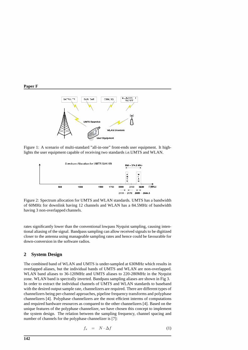
Paper F
���� ������
��� ������
���� ��������
��������� �� ! �� "�#! $" �%��&&�'!
(�" ��
Figure 1: A scenario of multi-standard ”all-in-one” front-ends user equipment. It high-lights the user equipment capable of receiving two standards i.e.UMTS and WLAN.
)*+,
- ./012344 5444 5344 6444 6344789: ;;9:
6554 65<4
=>?@
6A44 6ABAC3
DE F G<AC3 /01HIJKLMNO PQQRKSLTRU VRM WXYH Z[\P]
Figure 2: Spectrum allocation for UMTS and WLAN standards. UMTS has a bandwidthof 60MHz for downlink having 12 channels and WLAN has a 84.5MHz of bandwidthhaving 3 non-overlapped channels.
rates significantly lower than the conventional lowpass Nyquist sampling, causing inten-tional aliasing of the signal. Bandpass sampling can allow received signals to be digitizedcloser to the antenna using manageable sampling rates and hence could be favourable fordown-conversion in the software radios.
2 System Design
The combined band of WLAN and UMTS is under-sampled at 630MHzwhich results inoverlapped aliases, but the individual bands of UMTS and WLAN are non-overlapped.WLAN band aliases to 36-120MHz and UMTS aliases to 220-280MHz in the Nyquistzone. WLAN band is spectrally inverted. Bandpass sampling aliases are shown in Fig 3.In order to extract the individual channels of UMTS and WLAN standards to basebandwith the desired output sample rate, channelizers are required. There are different types ofchannelizers being per-channel approaches, pipeline frequency transforms and polyphasechannelizers [4]. Polyphase channelizers are the most efficient interms of computationsand required hardware resources as compared to the other channelizers [4]. Based on theunique features of the polyphase channelizer, we have chosen this concept to implementthe system design. The relation between the sampling frequency, channel spacing andnumber of channels for the polyphase channelizer is [7]:
fs = N ·∆f (1)
142

2 System Design
���
���� ����
�� �� �
��������
�� � ���
��
���
���
���
� � ������� ��� ��� ���
�
� !"# !"#
��$
% !"#
&�$ �$�$
' !"#
���$
��
��� ������
� !"# ()*
+,-.
+,-. /0123425
6789
6789 /0123425
9:;<=!4 >?02��$
Figure 3: The combined band of UMTS and WLAN is undersampled at 630MHz, and thealiased signals are shown in the Nyquist zones. The aliases are overlapped but individualUMTS and WLAN bands are non-overlapped. WLAN alias is spectrally inverted in theNyquist zone.
wherefs is the input sampling frequency,N is the number of channels (i.e., transformsize) and∆f is the inter-channel spacing. There are two constraints that have to bemet; one is thatN should be an integer, and the second is that the channels to bedown-sampled and down-converted to baseband should be centered onto the multiples of thechannel spacing.
The block diagram of the system design [5] having a sampling frequency of 630MHzis shown in Fig. 4. The selection of the sampling frequency isan iterative process thatrequires the conditions of non-overlap aliases and polyphase channelizer constraints tobe fulfilled. The block diagram shows a dual-standard system, sampling at 630MHz andusing bandpass filters to separate the two standards before channelization. In order toreduce the computational workload of the polyphase filters,the incoming complex sig-nals from the bandpass filters are down-sampled by possible large factors such that thesampling frequency of the re-sampled signals is above the signal’s bandwidth.
@ABCDAEE
FGH
@FIGJFKK
LMNOPQ
@FIGJFKK
LMNOPQ
RSTU
JVNWJXFKP
HXFIIPNMYPQ
@AEZ[ABC
J\]^ZEE_B`
abcd
JVNWJXFKP
HXFIIPNMYPQ
HeABBZf KZfZ^g]\
RSTU
abcd
QPh
KFiJNPQ
QPh
KFiJNPQ
@ABCDAEE KAjDf_B`
k lmn bop
H]j[_BZ [ABC ]q
riOK s tNFI
uvwwx h vyzy{ iX|u}~hwvx{ iX|
uvvxhvzx{ iX|
i � �
i � �
�x iX|
�x iX| V�gD�g \AgZ
��n bop
V�gD�g \AgZ
�l���� bop�� bop
T��������
���������
qEw
qEv
HeABBZf KZfZ^g]\
Figure 4: System block diagram having spectrum translationprior to UMTS and WLANchannelizers. UMTS channelizer is followed by Arbitrary Resampler to achieve the targetrate of 61.44MHz [5].
In an SDR receiver chain, after the ADC we need to have IQ demodulators to have
143

Paper F
quadrature signals needed to perform the filtering task on complex data. The well knownmethods for IQ demodulations are quadrature mixer which is known as Digital DownConverter (DDC), complex filtering and Hilbert transform methods [10]. Irrespectiveof their performance characteristics, in all of these casesmultipliers operate and deliverthe output at the same rate as the input. SDR based applications demand high samplingrates to eliminate most of the analog components. It will require not only the technologyadvancements but especially the advanced signal processing methods to handle and effi-ciently process the high sample rate data with the current technology.
This paper will focus on the bandpass filters used in a multi-standard system design [5].High sampling rate at the input leads to the problems of complicated ADC-FPGA inter-faces, and the design of bandpass filters which should operate at high rate. These prob-lems can be solved by splitting the data stream in multiple paths and feeding the data to thepolyphase channelizer. The split data drives the commutator (a rotatary switch distribut-ing the data among the various arm (sub-filter) in the polyphase filter) of the polyphasechannelizer [9] and reduces the per-arm data rate. The next task is to design the polyphaseprototype filter to extract the band of channels (standards)rather than single channels. Itwill be helpful in two folds. First, we do not need to have an IQdemodulator at the inputwhich is the high frequency end. Second, the bandpass filter operates at a low frequencydue to the down-sampling at the commutator which further canbe configured to deliverthe required output sample rate by using embedded resampling (an efficient technique toresample the data in the polyphase arms rather than using separate P/Q resamplers).
A channelizer described in [8] gives a proof-of-concept implementation, operating at a1.6GHz input signal. The input signal is split in parallel paths, lowering the per-arm fre-quency and then fed to the polyphase channelizer. The high speed demands of 1.6GHzchannelizer are efficiently satisfied using the Xilinx Virtex-4 FPGA by using the DSP48blocks capable of operating at 500MHz [11]. The input signalis quickly fanned-out to 16synchronized and parallel paths, effectively reducing theindividual path rates. In this casethe polyphase channelizer is efficiently used at the high input sampling rate, extractingthe individual channels. We will extend its use to act as bandpass filter having the samecharacteristics in terms of the low operating frequency andsplit data paths. Referring tothe multi-standard system design whose block diagram is shown in Fig. 4. The systemuses the undersampling technique and aliases down the combined spectrum of UMTS andWLAN, resulting in overlapped aliases but the individual bands of UMTS and WLAN arestill non-overlapped. The channel bandwidth of both standards is different thus requiringseparate channelizers. Therefore it requires bandpass filters to separate the standards be-fore the channelizers as shown in Fig. 4.
For a polyphase channelizer to act as a bandpass filter, we follow the same procedure,i.e., split the frequency spectrum in equal spectral bins and try to choose a factorN thatmeets thefs = N ·∆f requirements in terms of the channel spectral allocation and non-overlapped channels. Furthermore, the polyphase channelizer can be used in its variantmode where the channels’ bin can be shifted by multiples of quarter of the channel spac-ing [9] in order to have a better channel filtering operation.The filter requirements forUMTS and WLAN standards are shown in Fig. 5.
144
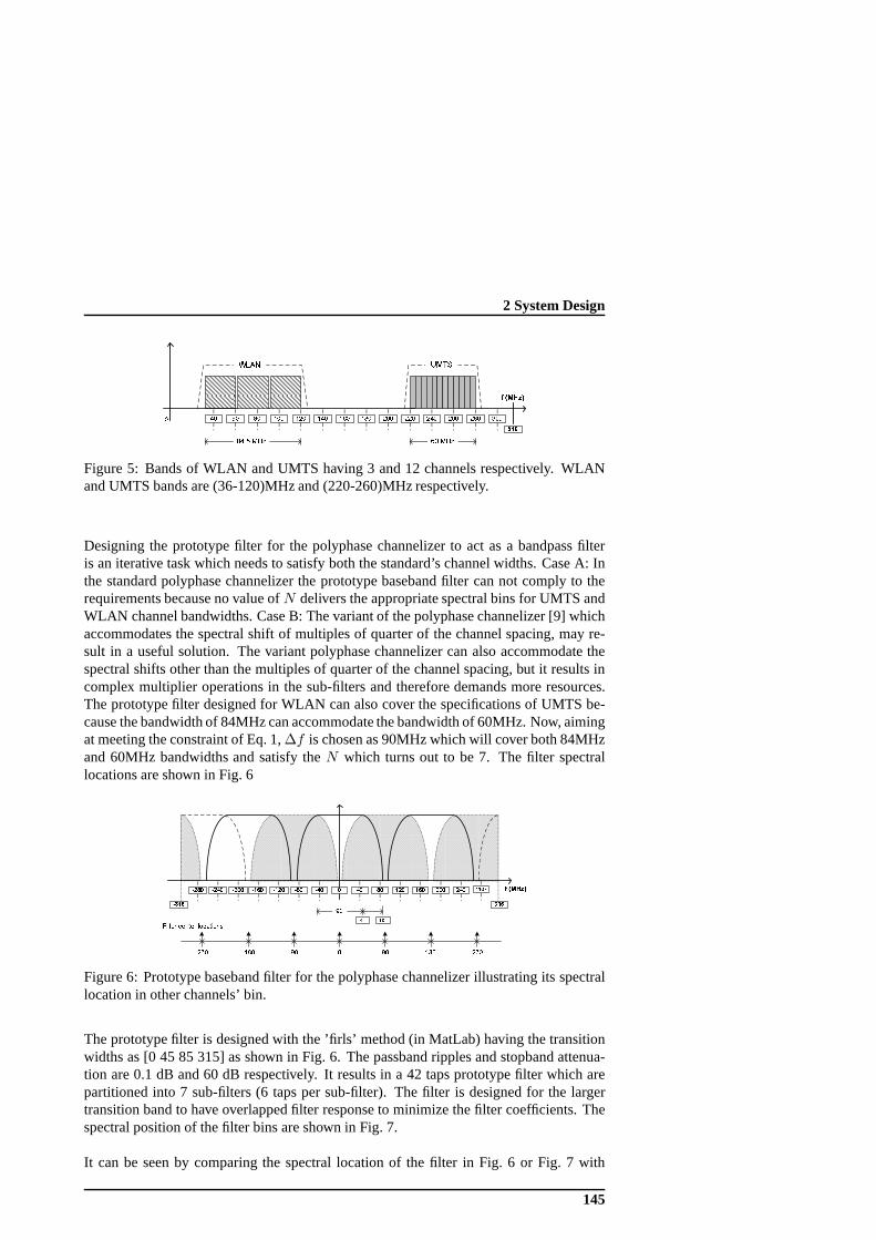
2 System Design
� ��������� ���
���
���
�� �
�� �� �� ��� ��������� ��� ���
����
�� ������� ���
���
Figure 5: Bands of WLAN and UMTS having 3 and 12 channels respectively. WLANand UMTS bands are (36-120)MHz and (220-260)MHz respectively.
Designing the prototype filter for the polyphase channelizer to act as a bandpass filteris an iterative task which needs to satisfy both the standard’s channel widths. Case A: Inthe standard polyphase channelizer the prototype basebandfilter can not comply to therequirements because no value ofN delivers the appropriate spectral bins for UMTS andWLAN channel bandwidths. Case B: The variant of the polyphase channelizer [9] whichaccommodates the spectral shift of multiples of quarter of the channel spacing, may re-sult in a useful solution. The variant polyphase channelizer can also accommodate thespectral shifts other than the multiples of quarter of the channel spacing, but it results incomplex multiplier operations in the sub-filters and therefore demands more resources.The prototype filter designed for WLAN can also cover the specifications of UMTS be-cause the bandwidth of 84MHz can accommodate the bandwidth of 60MHz. Now, aimingat meeting the constraint of Eq. 1,∆f is chosen as 90MHz which will cover both 84MHzand 60MHz bandwidths and satisfy theN which turns out to be 7. The filter spectrallocations are shown in Fig. 6
!""#$"#!" !%"
&'(
)" * +,-./0#$" 0%"0)"0#!" %"
12
!)"0!""0!%"0!)"
3&'(
%4 )4
2 12 562 78291295629782
:;<=>? @>A=>? <B@C=;BAD
E
Figure 6: Prototype baseband filter for the polyphase channelizer illustrating its spectrallocation in other channels’ bin.
The prototype filter is designed with the ’firls’ method (in MatLab) having the transitionwidths as [0 45 85 315] as shown in Fig. 6. The passband ripplesand stopband attenua-tion are 0.1 dB and 60 dB respectively. It results in a 42 taps prototype filter which arepartitioned into 7 sub-filters (6 taps per sub-filter). The filter is designed for the largertransition band to have overlapped filter response to minimize the filter coefficients. Thespectral position of the filter bins are shown in Fig. 7.
It can be seen by comparing the spectral location of the filterin Fig. 6 or Fig. 7 with
145
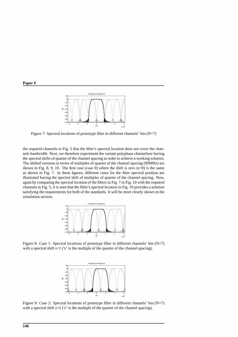
Paper F
−3 −2 −1 0 1 2 3
x 108
−70
−60
−50
−40
−30
−20
−10
0
10Frequency Response
Hz
dB
Figure 7: Spectral locations of prototype filter in different channels’ bin (N=7)
the required channels in Fig. 5 that the filter’s spectral location does not cover the chan-nels bandwidth. Next, we therefore experiment the variant polyphase channelizer havingthe spectral shifts of quarter of the channel spacing in order to achieve a working solution.The shifted versions in terms of multiples of quarter of the channel spacing (90MHz) areshown in Fig. 8, 9, 10. The first case (case 0) where the shift iszero (s=0) is the sameas shown in Fig. 7. In these figures, different cases for the filter spectral position areillustrated having the spectral shift of multiples of quarter of the channel spacing. Now,again by comparing the spectral location of the filters in Fig. 7 to Fig. 10 with the requiredchannels in Fig. 5, it is seen that the filter’s spectral location in Fig. 10 provides a solutionsatisfying the requirements for both of the standards. It will be more clearly shown in thesimulation section.
−3 −2 −1 0 1 2 3
x 108
−70
−60
−50
−40
−30
−20
−10
0
10Frequency Response
Hz
dB
Figure 8: Case 1: Spectral locations of prototype filter in different channels’ bin (N=7)with a spectral shift s=1 (’s’ is the multiple of the quarter of the channel spacing).
−3 −2 −1 0 1 2 3
x 108
−70
−60
−50
−40
−30
−20
−10
0
10Frequency Response
Hz
dB
Figure 9: Case 2: Spectral locations of prototype filter in different channels’ bin (N=7)with a spectral shift s=2 (’s’ is the multiple of the quarter of the channel spacing).
146

3 Simulations
−3 −2 −1 0 1 2 3
x 108
−70
−60
−50
−40
−30
−20
−10
0
10Frequency Response
Hz
dB
Figure 10: Case 3: Spectral locations of prototype filter in different channels’ bin (N=7)with a spectral shift s=3 (’s’ is the multiple of the quarter of the channel spacing).
If even by these two solutions (case A & B), the filter requirements of both standards arenot met, then variant polyphase channelizer having spectral shifts other than multiplesof the quarter of the channel spacing can be employed. As explain earlier, that it willincrease to the required resource utilization but the design will have characteristics oflow operating frequency and multiple path input data which is the most important whileworking with the high frequency input data.
3 Simulations
In order to simulate the working of the design, we have generated a composite test signalat the spectral locations of WLAN and UMTS standards which isshown in Fig. 11.
0 0.5 1 1.5 2 2.5 3
x 108
−60
−40
−20
0
Input signal Spectrum @ 630MHz
Hz
dB
Figure 11: A composite test signal generated at the spectrallocations of WLAN andUMTS standards. WLAN has 3 non-overlapped channels whereasUMTS has 12 chan-nels.
This test signal is applied to the variant polyphase channelizer havings = 3 as shownabove, which delivers the required UMTS and WLAN bands at theoutput. The inputsignal’s spectrum overlaid with the filter’s spectral positions for the variant polyphasechannelizer withs = 3 which gives a solution in this case as shown in Fig. 12. It canbe seen that UMTS and WLAN bands are well occupied by the filter’s passband only inchannel 1 and 3.
All 7 channel outputs of the channelizers are shown in Fig. 13. It can be seen that onlyoutputs from channel 1 and 3 delivers the required outputs asbandpass filters for UMTSand WLAN standards. The remaining outputs are garbage beingmixtures of both the
147

Paper F
−3 −2 −1 0 1 2 3
x 108
−70
−60
−50
−40
−30
−20
−10
0
10Input signal overlapped with filter response
Hz
dB
Channel # 3Channel # 1
Figure 12: The input signal spectrum is overlaid with the filter’s spectral positions forvariant polyphase channelizer withs = 3.
standards. The outputs have sample rate of 90MHz which is dueto down-sampling by 7in the commutator. Furthermore the outputs from the variantpolyphase channelizer are
−4 −2 0 2 4
x 107
−50
0Channel 1
dB
−4 −2 0 2 4
x 107
−50
0Channel 2
−4 −2 0 2 4
x 107
−50
0Channel 3
dB
−4 −2 0 2 4
x 107
−50
0Channel 4
−4 −2 0 2 4
x 107
−50
0Channel 5
dB
−4 −2 0 2 4
x 107
−50
0Channel 6
Hz
−4 −2 0 2 4
x 107
−50
0Channel 7
Hz
dB
Figure 13: All 7 Channel outputs of the channelizers. It can be seen that only outputsfrom the channel 1 and 3 deliver the required outputs as bandpass filters for the UMTSand WLAN standards.
complex which therefore eliminate the need of IQ demodulators in this case. WLAN andUMTS bandpass signals are spectrally shifted byΠ andΠ/2 rotators respectively to havea clear view of bandpass outputs as shown in Fig. 14. These shifting will not require any
148

4 Conclusion
real multiplication operation asΠ andΠ/2 rotators result only in sign change operation.So we have efficiently bandpass filtered UMTS and WLAN standards at input samplingrate of 630MHz and delivering the outputs at 90MHz.
−4 −2 0 2 4
x 107
−60
−40
−20
0WLAN Channels
dB
−4 −2 0 2 4
x 107
−60
−40
−20
0Shifted WLAN Channels
−4 −2 0 2 4
x 107
−60
−40
−20
0UMTS Channels
dB
Hz−4 −2 0 2 4
x 107
−60
−40
−20
0Shifted UMTS Channels
Hz
Figure 14: WLAN and UMTS bandpass signals are spectrally shifted by Π andΠ/2rotators to have a more clear view of the bandpass signals. These shifting will not requireany multiplication operation.
4 Conclusion
A dual-standard (UMTS & WLAN) software radio receiver architecture is presented withthe focus on high performance bandpass filters. It is required to have bandpass filters toseparate out the standards before channelization such thatthey can handle the high inputdata stream and can operate on the current technology platforms as well. It is seen thatthe polyphase channelizer or its variant can be used with their unique and extraordinaryfeatures of multiple paths and spectral translation, to actas a high performance bandpassfilter which can also eliminate the need for IQ demodulators.The final system blockdiagram is shown in Fig. 15 where the previous bandpass filters for UMTS and WLANstandards in Fig. 4 are removed by a single polyphase channelizer, making the architecturemore compact and resource efficient. The initial estimates for resource utilization resultin approx. 32% of reduction compared to the solution with separate bandpass filtersimplemented in polyphase fashion as well.
��������
���
�� ���
� ���������
���������
�������
����
�� ���
� ���������
���� ���
�!"�����#
$%&'
�� ���
� ���������
�(����� ����"�!�
����
$%&'
�������� ��)����#
* +,- %./
�!) ��� ��� !�
012� 3 4���
�5667 8 59:9� 1 ;
<=>?@ABC DEF
<AAB?AGBC DEF
H7 1 ;
I7 1 ;
J��J� ����
KL- %./
J��J� ����
K+MNOO %./KP %./
�QRSTQUQV
WXYUZ[\XQ
��6
��5
�(����� ����"�!�
Figure 15: Final system block diagram where the previous bandpass filters for UMTS andWLAN standards are removed by a single polyphase channelizer.
149

Paper F
References
[1] Mehmood-ur-Rehman Awan, Muhammad Mahtab Alam, ”Design& Implementationof FPGA-based Multi-standard Software Radio Receiver”, inProc. IEEE NorchipConference on microelectronic, Nov. 2007
[2] B. Razavi, ”Challenges and trends in RF design”, inProc. IEEE ASIC Conf. andExhibit, 1996, pp. 81-86
[3] Stream radio goes digital. http://www.csdr.dk.
[4] Mehmood-ur-Rehman Awan, Muhammad Mahtab Alam, ”Design& Implementationof FPGA-based Multi-standard Software Radio Receiver”, Master of EngineeringThesis, Aalborg University Denmark, June 2007
[5] Mehmood-ur-Rehman Awan, Muhammad Mahtab Alam, ”Area efficient implemen-tation of polyphase channelizer for Multi-standard Software Radio”, 5th KarlsruheWorkshop on Software Radios, 2008.
[6] Patel, M. and Lane, P., ”Comparison of downconversion techniques for software ra-dio”, Department of Electronics and Electrical Engineering, University College Lon-don. www.ee.ucl.ac.uk/lcs/papers2000/lcs050.pdf.
[7] Fredric J. Harris, Chris Dick and Micheal Rice, ”Digitalreceivers and Transmittersusing Polyphase Filter Banks for Wireless Communications”, in IEEE Transactionon microwave theory and techniques, Vol. 51, No. 4 April 2003
[8] Benjamin Egg, Fredric J. Harris, Chris Dick, ”Ultra-Wideband 1.6GHz Channelizer:Versatile FPGA Implementation”, inProceedings of the SDR 05 Technical Confer-ence and Product Exposition, SDR Forum, 2005
[9] fredric j. harris,Multirate Signal Processing for Communication Systems, PrenticeHall, 2006
[10] Richard G. Lyons,Understanding Digital Signal Processing, Prentice Hall, SecondEdition, 2004 ISBN-10: 0-13-108989-7
[11] http://www.xilinx.com
150