![Phos-Chek 3% AFFF MS - [AQUAFILM AF-3MS] … 3% AFFF MS - [AQUAFILM AF-3MS] Safety data sheet According to 1907/2006/EC (REACH), 453/2010/EU, 2015/830/EU SECTION 1: IDENTIFICATION](https://static.fdocuments.in/doc/165x107/5b0ac18c7f8b9ae61b8c958c/phos-chek-3-afff-ms-aquafilm-af-3ms-3-afff-ms-aquafilm-af-3ms-safety-data.jpg)
A25L080/A25L040 Series - search...
41
A25L080/A25L040 Series 8Mbit / 4Mbit Low Voltage, Serial Flash Memory Preliminary With 85MHz Uniform 4KB Sectors PRELIMINARY (July, 2007, Version 0.0) AMIC Technology Corp. Document Title 8Mbit / 4Mbit, Low Voltage, Serial Flash Memory With 85MHz Uniform 4KB Sectors Revision History Rev. No. History Issue Date Remark 0.0 Initial issue July 9, 2007 Preliminary
Transcript of A25L080/A25L040 Series - search...
A25L080/A25L040 Series
8Mbit / 4Mbit Low Voltage, Serial Flash Memory Preliminary With 85MHz Uniform 4KB Sectors
PRELIMINARY (July, 2007, Version 0.0) AMIC Technology Corp.
Document Title 8Mbit / 4Mbit, Low Voltage, Serial Flash Memory With 85MHz Uniform 4KB Sectors
Revision History
Rev. No. History Issue Date Remark 0.0 Initial issue July 9, 2007 Preliminary

A25L080/A25L040 Series
8Mbit / 4Mbit Low Voltage, Serial Flash Memory Preliminary With 85MHz Uniform 4KB Sectors
PRELIMINARY (July, 2007, Version 0.0) 1 AMIC Technology Corp.
FEATURES Family of Serial Flash Memories
- A25L080: 8M-bit /1M-byte - A25L040: 4M-bit /512K-byte
Flexible Sector Architecture with 4KB sectors - Sector Erase (4K-bytes) in 0.4s (typical) - Block Erase (64K-bytes) in 1s (typical)
Page Program (up to 256 Bytes) in 3ms (typical) 2.7 to 3.6V Single Supply Voltage SPI Bus Compatible Serial Interface 85MHz Clock Rate (maximum) Deep Power-down Mode 1µA (typical)
Electronic Signatures - JEDEC Standard Two-Byte Signature
A25L080: (3014h) A25L040: (3013h)
- RES Instruction, One-Byte, Signature, for backward compatibility A25L080 (13h) A25L040 (12h)
Package options - 8-pin SOP (209mil), 8-pin DIP (300mil) or 8-pin DFN8 - All Pb-free (Lead-free) products are RoHS compliant
GENERAL DESCRIPTION
The A25L080/A25L040 are 8M/4M bit Serial Flash Memory, with advanced write protection mechanisms, accessed by a high speed SPI-compatible bus. The memory can be programmed 1 to 256 bytes at a time, using the Page Program instruction. The memory is organized as 16/8(A25L080/A25L040) blocks, each containing 16 sectors. Each sector is composed of 16
pages. Each page is 256 bytes wide. Thus, the whole memory can be viewed as consisting of 4096/2048(A25L080/A25L040) pages, or 1048,576/524,288(A25L080/A25L040) bytes. The whole memory can be erased using the Chip Erase instruction, a block at a time, using Block Erase instruction, or a sector at a time, using the Sector Erase instruction.
Pin Configurations
SOP8 Connections DIP8 Connections
VCC
CQ
D
S
WHOLD
VSS
1 82 73 64 5
A25L080/A25L040
A25L080/A25L040
VCC
CQ
D
S
WHOLD
VSS
1 82 73 64 5
A25L080/A25L040 Series
PRELIMINARY (July, 2007, Version 0.0) 2 AMIC Technology Corp.
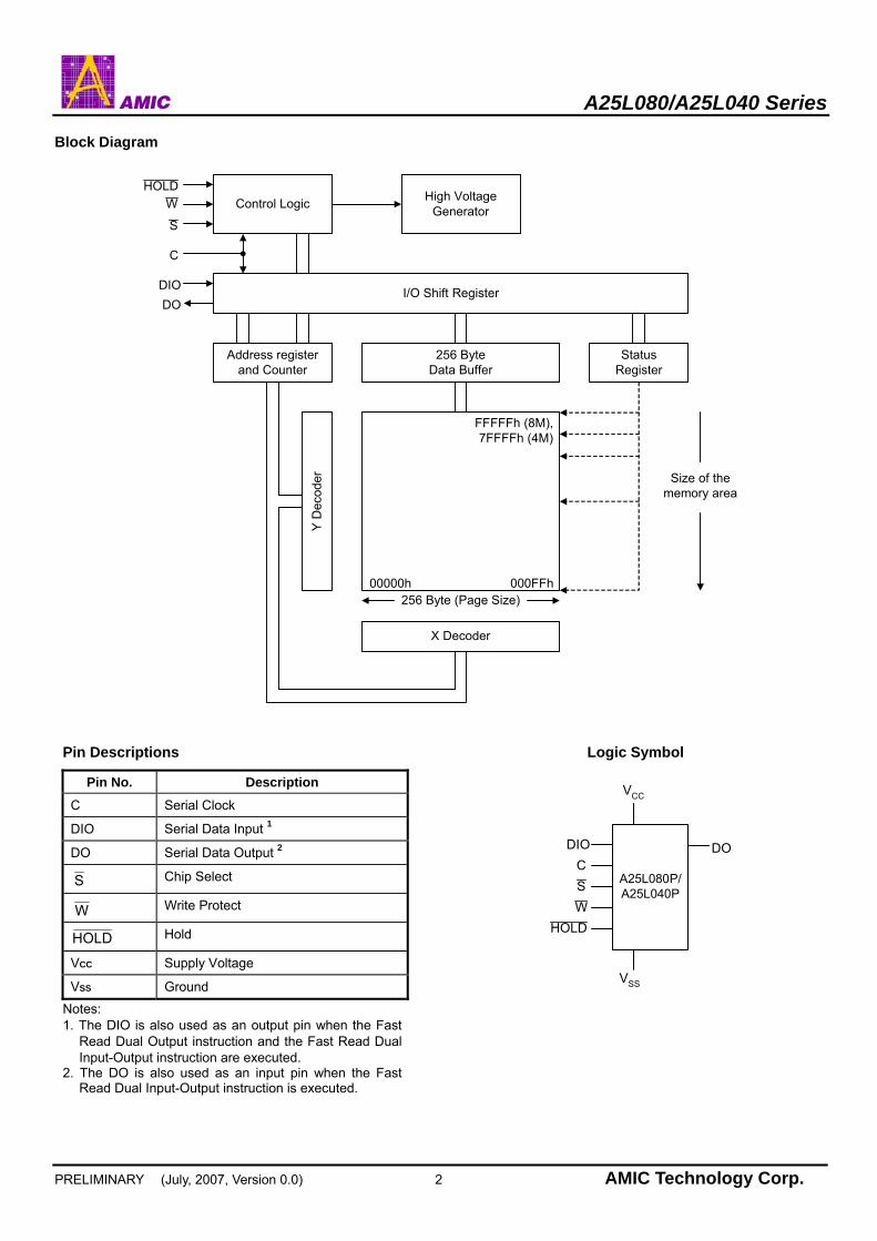
Block Diagram
Control Logic High VoltageGenerator
I/O Shift Register
Address registerand Counter
256 ByteData Buffer
StatusRegister
X Decoder
256 Byte (Page Size)
Y D
ecod
er Size of thememory area
DIODO
C
000FFh00000h
HOLDW
S
FFFFFh (8M),7FFFFh (4M)
Pin Descriptions
Pin No. Description
C Serial Clock
DIO Serial Data Input 1
DO Serial Data Output 2
S Chip Select
W Write Protect
HOLD Hold
VCC Supply Voltage
VSS Ground Notes: 1. The DIO is also used as an output pin when the Fast
Read Dual Output instruction and the Fast Read Dual Input-Output instruction are executed.
2. The DO is also used as an input pin when the Fast Read Dual Input-Output instruction is executed.
Logic Symbol
A25L080P/A25L040P
DODIO
SW
HOLD
VSS
VCC
C

A25L080/A25L040 Series
PRELIMINARY (July, 2007, Version 0.0) 3 AMIC Technology Corp.
SIGNAL DESCRIPTION Serial Data Output (DO). This output signal is used to transfer data serially out of the device. Data is shifted out on the falling edge of Serial Clock (C). The DO pin is also used as an input pin when the Fast Read Dual Input-Output instruction is executed. Serial Data Input (DIO). This input signal is used to transfer data serially into the device. It receives instructions, addresses, and the data to be programmed. Values are latched on the rising edge of Serial Clock (C). The DIO pin is also used as an output pin when the Fast Read Dual Output instruction and the Fast Read Dual Input-Output instruction are executed. Serial Clock (C). This input signal provides the timing of the serial interface. Instructions, addresses, or data present at Serial Data Input (DIO) are latched on the rising edge of Serial Clock (C). Data on Serial Data Output (DO) changes after the falling edge of Serial Clock (C). Chip Select (S ). When this input signal is High, the device is deselected and Serial Data Output (DO) is at high
impedance. Unless an internal Program, Erase or Write Status Register cycle is in progress, the device will be in the Standby mode (this is not the Deep Power-down mode). Driving Chip Select (S ) Low enables the device, placing it in the active power mode. After Power-up, a falling edge on Chip Select (S ) is required prior to the start of any instruction. Hold (HOLD ). The Hold (HOLD ) signal is used to pause any serial communications with the device without deselecting the device. During the Hold condition, the Serial Data Output (DO) is high impedance, and Serial Data Input (DIO) and Serial Clock (C) are Don’t Care. To start the Hold condition, the device must be selected, with Chip Select (S ) driven Low. Write Protect ( W ). The main purpose of this input signal is to freeze the size of the area of memory that is protected against program or erase instructions (as specified by the values in the BP2, BP1, and BP0 bits of the Status Register).

A25L080/A25L040 Series
PRELIMINARY (July, 2007, Version 0.0) 4 AMIC Technology Corp.
SPI MODES
These devices can be driven by a microcontroller with its SPI peripheral running in either of the two following modes: – CPOL=0, CPHA=0 – CPOL=1, CPHA=1 For these two modes, input data is latched in on the rising edge of Serial Clock (C), and output data is available from the
falling edge of Serial Clock (C). The difference between the two modes, as shown in Figure 2, is the clock polarity when the bus master is in Stand-by mode and not transferring data: – C remains at 0 for (CPOL=0, CPHA=0) – C remains at 1 for (CPOL=1, CPHA=1)
Figure 1. Bus Master and Memory Devices on the SPI Bus
Bus Master(ST6, ST7, ST9,
ST10, Other)
SPI Interface with(CPOL, CPHA)= (0, 0) or (1, 1)
CS3 CS2 CS1
SPI MemoryDevice
C DO DIO
S W HOLD
SPI MemoryDevice
S W HOLD
SPI MemoryDevice
S W HOLD
SDISDO
SCK
C DO DIO C DO DIO
Note: The Write Protect ( W ) and Hold (HOLD ) signals should be driven, High or Low as appropriate.
Figure 2. SPI Modes Supported
MSB
MSB
C
C
DIO
DO
0 0
11
CPOL CPHA

A25L080/A25L040 Series
PRELIMINARY (July, 2007, Version 0.0) 5 AMIC Technology Corp.
OPERATING FEATURES
Page Programming To program one data byte, two instructions are required: Write Enable (WREN), which is one byte, and a Page Program (PP) sequence, which consists of four bytes plus data. This is followed by the internal Program cycle (of duration tPP). To spread this overhead, the Page Program (PP) instruction allows up to 256 bytes to be programmed at a time (changing bits from 1 to 0), provided that they lie in consecutive addresses on the same page of memory.
Sector Erase, Block Erase, and Chip Erase The Page Program (PP) instruction allows bits to be reset from 1 to 0. Before this can be applied, the bytes of memory need to have been erased to all 1s (FFh). This can be achieved, a sector at a time, using the Sector Erase (SE) instruction, a block at a time, using the Block Erase (BE) instruction, or throughout the entire memory, using the Chip Erase (CE) instruction. This starts an internal Erase cycle (of duration tSE, tBE, or tCE). The Erase instruction must be preceded by a Write Enable (WREN) instruction.
Polling During a Write, Program or Erase Cycle A further improvement in the time to Write Status Register (WRSR), Program (PP) or Erase (SE, BE, or CE) can be achieved by not waiting for the worst case delay (tW, tPP, tSE, tBE, tCE). The Write In Progress (WIP) bit is provided in the Status Register so that the application program can monitor its value, polling it to establish when the previous Write cycle, Program cycle or Erase cycle is complete.
Active Power, Stand-by Power and Deep Power-Down Modes
When Chip Select (S ) is Low, the device is enabled, and in the Active Power mode. When Chip Select (S ) is High, the device is disabled, but could remain in the Active Power mode until all internal cycles have completed (Program, Erase, Write Status Register). The device then goes in to the Stand-by Power mode. The device consumption drops to ICC1. The Deep Power-down mode is entered when the specific instruction (the Deep Power-down Mode (DP) instruction) is executed. The device consumption drops further to ICC2. The device remains in this mode until another specific instruction (the Release from Deep Power-down Mode and Read Electronic Signature (RES) instruction) is executed. All other instructions are ignored while the device is in the Deep Power-down mode. This can be used as an extra software protection mechanism, when the device is not in active use, to protect the device from inadvertent Write, Program or Erase instructions.
Status Register The Status Register contains a number of status and control bits that can be read or set (as appropriate) by specific instructions. WIP bit. The Write In Progress (WIP) bit indicates whether the memory is busy with a Write Status Register, Program or Erase cycle. WEL bit. The Write Enable Latch (WEL) bit indicates the status of the internal Write Enable Latch. BP2, BP1, BP0 bits. The Block Protect (BP2, BP1, BP0) bits are non-volatile. They define the size of the area to be software protected against Program and Erase instructions. SRWD bit. The Status Register Write Disable (SRWD) bit is operated in conjunction with the Write Protect ( W ) signal. The Status Register Write Disable (SRWD) bit and Write Protect ( W ) signal allow the device to be put in the Hardware Protected mode. In this mode, the non-volatile bits of the Status Register (SRWD, BP2, BP1, BP0) become read-only bits.
Protection Modes The environments where non-volatile memory devices are used can be very noisy. No SPI device can operate correctly in the presence of excessive noise. To help combat this, the A25L080/A25L040 boasts the following data protection mechanisms:
Power-On Reset and an internal timer (tPUW) can provide protection against inadvertant changes while the power supply is outside the operating specification.
Program, Erase and Write Status Register instructions are checked that they consist of a number of clock pulses that is a multiple of eight, before they are accepted for execution.
All instructions that modify data must be preceded by a Write Enable (WREN) instruction to set the Write Enable Latch (WEL) bit. This bit is returned to its reset state by the following events: - Power-up - Write Disable (WRDI) instruction completion - Write Status Register (WRSR) instruction completion - Page Program (PP) instruction completion - Sector Erase (SE) instruction completion - Block Erase (BE) instruction completion - Chip Erase (CE) instruction completion
The Block Protect (BP2, BP1, BP0) bits allow part of the memory to be configured as read-only. This is the Software Protected Mode (SPM).
The Write Protect ( W ) signal allows the Block Protect (BP2, BP1, BP0) bits and Status Register Write Disable (SRWD) bit to be protected. This is the Hardware Protected Mode (HPM).
In addition to the low power consumption feature, the Deep Power-down mode offers extra software protection from inadvertant Write, Program and Erase instructions, as all instructions are ignored except one particular instruction (the Release from Deep Power-down instruction).
A25L080/A25L040 Series
PRELIMINARY (July, 2007, Version 0.0) 6 AMIC Technology Corp.
Table 1. Protected Area Sizes
A25L080
Status Register Content Memory Content BP2 Bit BP1 Bit BP0 Bit Protected Area Unprotected Area
0 0 0 none All blocks1
0 0 1 Upper sixteenth (block: 15) Lower 15/16ths (15 blocks: 0 to 14)
0 1 0 Upper eighth (two blocks: 14 to 15) Lower seven-eighths (14 blocks: 0 to 13)
0 1 1 Upper quarter (four blocks: 12 to 15) Lower three-quarters (12 blocks: 0 to 11)
1 0 0 Upper half (eight blocks: 8 to 15) Lower half (8 blocks: 0 to 7)
1 0 1 All blocks (sixteen blocks: 0 to 15) None
1 1 0 All blocks (sixteen blocks: 0 to 15) None
1 1 1 All blocks (sixteen blocks: 0 to 15) None
Note: 1. The device is ready to accept a Chip Erase instruction if, and only if, all Block Protect (BP2, BP1, BP0) are 0. A25L040
Status Register Content Memory Content BP2 Bit BP1 Bit BP0 Bit Protected Area Unprotected Area
0 0 0 none All blocks1
0 0 1 Upper eighth (block: 7) Lower seven-eighths (7 blocks: 0 to 6)
0 1 0 Upper quarter (two blocks: 6 to 7) Lower three-quarters (6 blocks: 0 to 5)
0 1 1 Upper half (four blocks: 4 to 7) Lower half (4 blocks: 0 to 3)
1 0 0 All blocks (eight blocks: 0 to 7) None
1 0 1 All blocks (eight blocks: 0 to 7) None
1 1 0 All blocks (eight blocks: 0 to 7) None
1 1 1 All blocks (eight blocks: 0 to 7) None
Note: 1. The device is ready to accept a Chip Erase instruction if, and only if, all Block Protect (BP2, BP1, BP0) are 0.

A25L080/A25L040 Series
PRELIMINARY (July, 2007, Version 0.0) 7 AMIC Technology Corp.
Hold Condition The Hold ( HOLD ) signal is used to pause any serial communications with the device without resetting the clocking sequence. However, taking this signal Low does not terminate any Write Status Register, Program or Erase cycle that is currently in progress. To enter the Hold condition, the device must be selected, with Chip Select (S ) Low. The Hold condition starts on the falling edge of the Hold (HOLD ) signal, provided that this coincides with Serial Clock (C) being Low (as shown in Figure 3.). The Hold condition ends on the rising edge of the Hold (HOLD ) signal, provided that this coincides with Serial Clock (C) being Low. If the falling edge does not coincide with Serial Clock (C) being Low, the Hold condition starts after Serial Clock (C) next goes Low. Similarly, if the rising edge does not coincide with Serial Clock (C) being Low, the Hold condition ends after
Serial Clock (C) next goes Low. This is shown in Figure 3. During the Hold condition, the Serial Data Output (DO) is high impedance, and Serial Data Input (DIO) and Serial Clock (C) are Don’t Care. Normally, the device is kept selected, with Chip Select (S ) driven Low, for the whole duration of the Hold condition. This is to ensure that the state of the internal logic remains unchanged from the moment of entering the Hold condition. If Chip Select (S ) goes High while the device is in the Hold condition, this has the effect of resetting the internal logic of the device. To restart communication with the device, it is necessary to drive Hold (HOLD ) High, and then to drive Chip Select (S ) Low. This prevents the device from going back to the Hold condition.
Figure 3. Hold Condition Activation
HoldCondition
(standard use)
HOLD
C
HoldCondition
(non-standard use)

A25L080/A25L040 Series
PRELIMINARY (July, 2007, Version 0.0) 8 AMIC Technology Corp.
A25L080 MEMORY ORGANIZATION The memory is organized as:
1,048,576 bytes (8 bits each) 16 64-Kbytes blocks 256 4-Kbytes sectors 4096 pages (256 bytes each).
Each page can be individually programmed (bits are programmed from 1 to 0). The device is Sector, Block, or Chip Erasable (bits are erased from 0 to 1) but not Page Erasable.
Table 2. Memory Organization
A25L080 Address Table
Block Sector Address Range 255 0FF000h 0FFFFFh …
…
… 15
240 0F0000h 0F0FFFh 239 0EF000h 0EFFFFh …
…
… 14
224 0E0000h 0E0FFFh 223 0DF000h 0DFFFFh …
…
… 13
208 0D0000h 0D0FFFh 207 0CF000h 0CFFFFh …
…
… 12
192 0C0000h 0C0FFFh 191 0BF000h 0BFFFFh …
…
… 11
176 0B0000h 0B0FFFh 175 0AF000h 0AFFFFh …
…
… 10
160 0A0000h 0A0FFFh 159 09F000h 09FFFFh …
…
… 9
144 090000h 090FFFh 143 08F000h 08FFFFh …
…
… 8
128 080000h 080FFFh 127 07F000h 07FFFFh …
…
… 7
112 070000h 070FFFh 111 06F000h 06FFFFh …
…
… 6
96 060000h 060FFFh 95 05F000h 05FFFFh …
…
… 5
80 050000h 050FFFh 79 04F000h 04FFFFh …
…
… 4
64 040000h 040FFFh 63 03F000h 03FFFFh …
…
… 3
48 030000h 030FFFh 47 02F000h 02FFFFh …
…
… 2
32 020000h 020FFFh 31 01F000h 01FFFFh …
…
… 1
16 010000h 010FFFh 15 00F000h 00FFFFh …
…
…
3 003000h 003FFFh 2 002000h 002FFFh 1 001000h 001FFFh
0
0 000000h 000FFFh
A25L080/A25L040 Series
PRELIMINARY (July, 2007, Version 0.0) 9 AMIC Technology Corp.
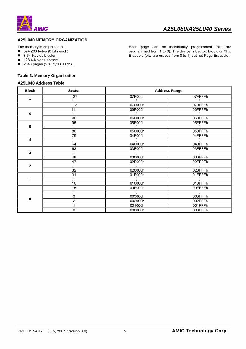
A25L040 MEMORY ORGANIZATION The memory is organized as:
524,288 bytes (8 bits each) 8 64-Kbytes blocks 128 4-Kbytes sectors 2048 pages (256 bytes each).
Each page can be individually programmed (bits are programmed from 1 to 0). The device is Sector, Block, or Chip Erasable (bits are erased from 0 to 1) but not Page Erasable.
Table 2. Memory Organization
A25L040 Address Table
Block Sector Address Range 127 07F000h 07FFFFh …
…
… 7
112 070000h 070FFFh 111 06F000h 06FFFFh …
…
… 6
96 060000h 060FFFh 95 05F000h 05FFFFh …
…
… 5
80 050000h 050FFFh 79 04F000h 04FFFFh …
…
… 4
64 040000h 040FFFh 63 03F000h 03FFFFh …
…
… 3
48 030000h 030FFFh 47 02F000h 02FFFFh …
…
… 2
32 020000h 020FFFh 31 01F000h 01FFFFh …
…
… 1
16 010000h 010FFFh 15 00F000h 00FFFFh …
…
…
3 003000h 003FFFh 2 002000h 002FFFh 1 001000h 001FFFh
0
0 000000h 000FFFh
A25L080/A25L040 Series
PRELIMINARY (July, 2007, Version 0.0) 10 AMIC Technology Corp.
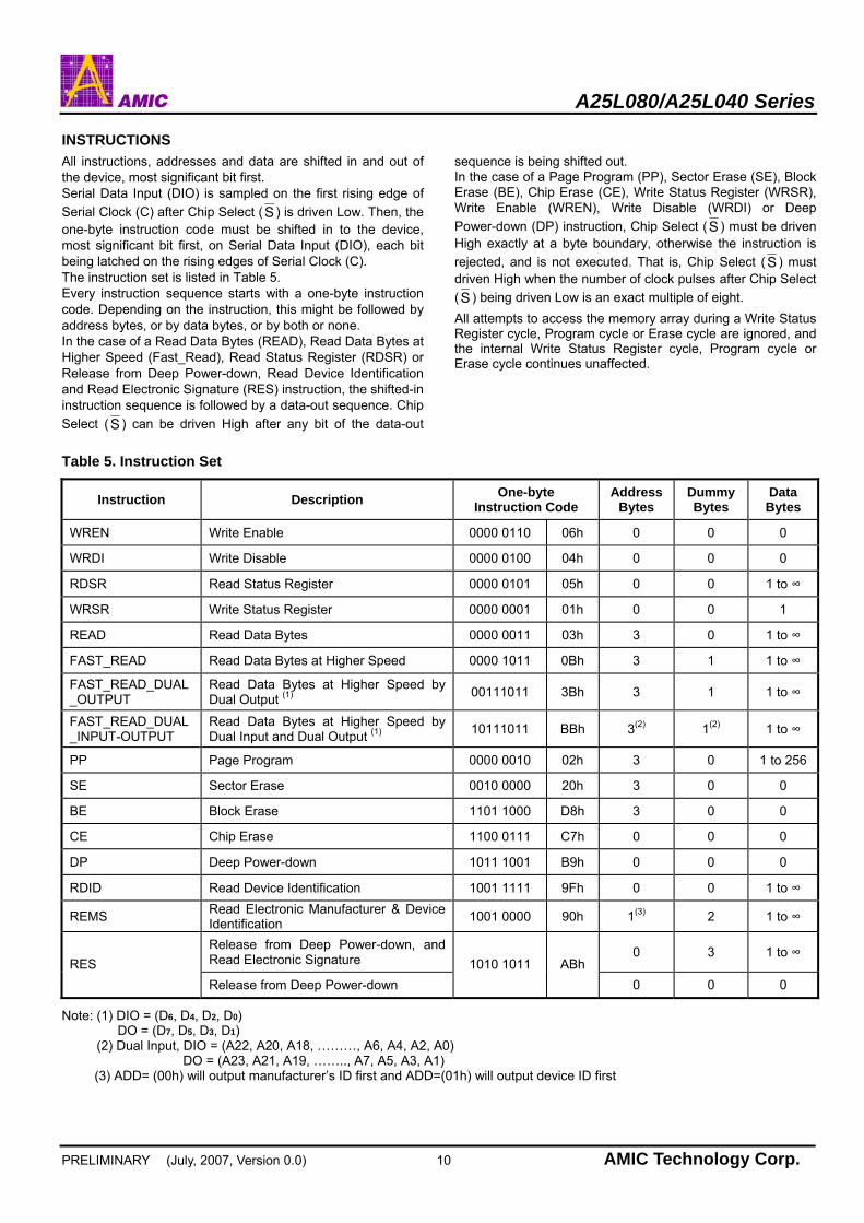
INSTRUCTIONS All instructions, addresses and data are shifted in and out of the device, most significant bit first. Serial Data Input (DIO) is sampled on the first rising edge of Serial Clock (C) after Chip Select (S ) is driven Low. Then, the one-byte instruction code must be shifted in to the device, most significant bit first, on Serial Data Input (DIO), each bit being latched on the rising edges of Serial Clock (C). The instruction set is listed in Table 5. Every instruction sequence starts with a one-byte instruction code. Depending on the instruction, this might be followed by address bytes, or by data bytes, or by both or none. In the case of a Read Data Bytes (READ), Read Data Bytes at Higher Speed (Fast_Read), Read Status Register (RDSR) or Release from Deep Power-down, Read Device Identification and Read Electronic Signature (RES) instruction, the shifted-in instruction sequence is followed by a data-out sequence. Chip Select (S ) can be driven High after any bit of the data-out
sequence is being shifted out. In the case of a Page Program (PP), Sector Erase (SE), Block Erase (BE), Chip Erase (CE), Write Status Register (WRSR), Write Enable (WREN), Write Disable (WRDI) or Deep Power-down (DP) instruction, Chip Select (S ) must be driven High exactly at a byte boundary, otherwise the instruction is rejected, and is not executed. That is, Chip Select (S ) must driven High when the number of clock pulses after Chip Select (S ) being driven Low is an exact multiple of eight. All attempts to access the memory array during a Write Status Register cycle, Program cycle or Erase cycle are ignored, and the internal Write Status Register cycle, Program cycle or Erase cycle continues unaffected.
Table 5. Instruction Set
Instruction Description One-byte Instruction Code
Address Bytes
Dummy Bytes
Data Bytes
WREN Write Enable 0000 0110 06h 0 0 0
WRDI Write Disable 0000 0100 04h 0 0 0
RDSR Read Status Register 0000 0101 05h 0 0 1 to ∞
WRSR Write Status Register 0000 0001 01h 0 0 1
READ Read Data Bytes 0000 0011 03h 3 0 1 to ∞
FAST_READ Read Data Bytes at Higher Speed 0000 1011 0Bh 3 1 1 to ∞
FAST_READ_DUAL_OUTPUT
Read Data Bytes at Higher Speed by Dual Output (1) 00111011 3Bh 3 1 1 to ∞
FAST_READ_DUAL_INPUT-OUTPUT
Read Data Bytes at Higher Speed by Dual Input and Dual Output (1) 10111011 BBh 3(2) 1(2) 1 to ∞
PP Page Program 0000 0010 02h 3 0 1 to 256
SE Sector Erase 0010 0000 20h 3 0 0
BE Block Erase 1101 1000 D8h 3 0 0
CE Chip Erase 1100 0111 C7h 0 0 0
DP Deep Power-down 1011 1001 B9h 0 0 0
RDID Read Device Identification 1001 1111 9Fh 0 0 1 to ∞
REMS Read Electronic Manufacturer & Device Identification 1001 0000 90h 1(3) 2 1 to ∞
Release from Deep Power-down, and Read Electronic Signature 0 3 1 to ∞
RES Release from Deep Power-down
1010 1011 ABh 0 0 0
Note: (1) DIO = (D6, D4, D2, D0) DO = (D7, D5, D3, D1) (2) Dual Input, DIO = (A22, A20, A18, ………, A6, A4, A2, A0) DO = (A23, A21, A19, …….., A7, A5, A3, A1) (3) ADD= (00h) will output manufacturer’s ID first and ADD=(01h) will output device ID first
A25L080/A25L040 Series
PRELIMINARY (July, 2007, Version 0.0) 11 AMIC Technology Corp.
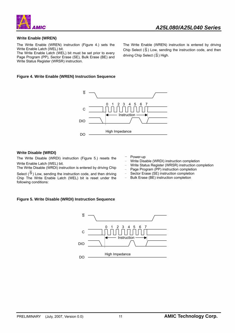
Write Enable (WREN) The Write Enable (WREN) instruction (Figure 4.) sets the Write Enable Latch (WEL) bit. The Write Enable Latch (WEL) bit must be set prior to every Page Program (PP), Sector Erase (SE), Bulk Erase (BE) and Write Status Register (WRSR) instruction.
The Write Enable (WREN) instruction is entered by driving Chip Select (S ) Low, sending the instruction code, and then driving Chip Select (S ) High.
Figure 4. Write Enable (WREN) Instruction Sequence
S
C
DIO
DOHigh Impedance
Instruction
0 1 2 3 4 5 6 7
Write Disable (WRDI) The Write Disable (WRDI) instruction (Figure 5.) resets the Write Enable Latch (WEL) bit. The Write Disable (WRDI) instruction is entered by driving Chip
Select (S ) Low, sending the instruction code, and then driving Chip The Write Enable Latch (WEL) bit is reset under the following conditions:
﹣ Power-up ﹣ Write Disable (WRDI) instruction completion ﹣ Write Status Register (WRSR) instruction completion ﹣ Page Program (PP) instruction completion ﹣ Sector Erase (SE) instruction completion ﹣ Bulk Erase (BE) instruction completion
Figure 5. Write Disable (WRDI) Instruction Sequence
S
C
DIO
DOHigh Impedance
Instruction
0 1 2 3 4 5 6 7
A25L080/A25L040 Series
PRELIMINARY (July, 2007, Version 0.0) 12 AMIC Technology Corp.
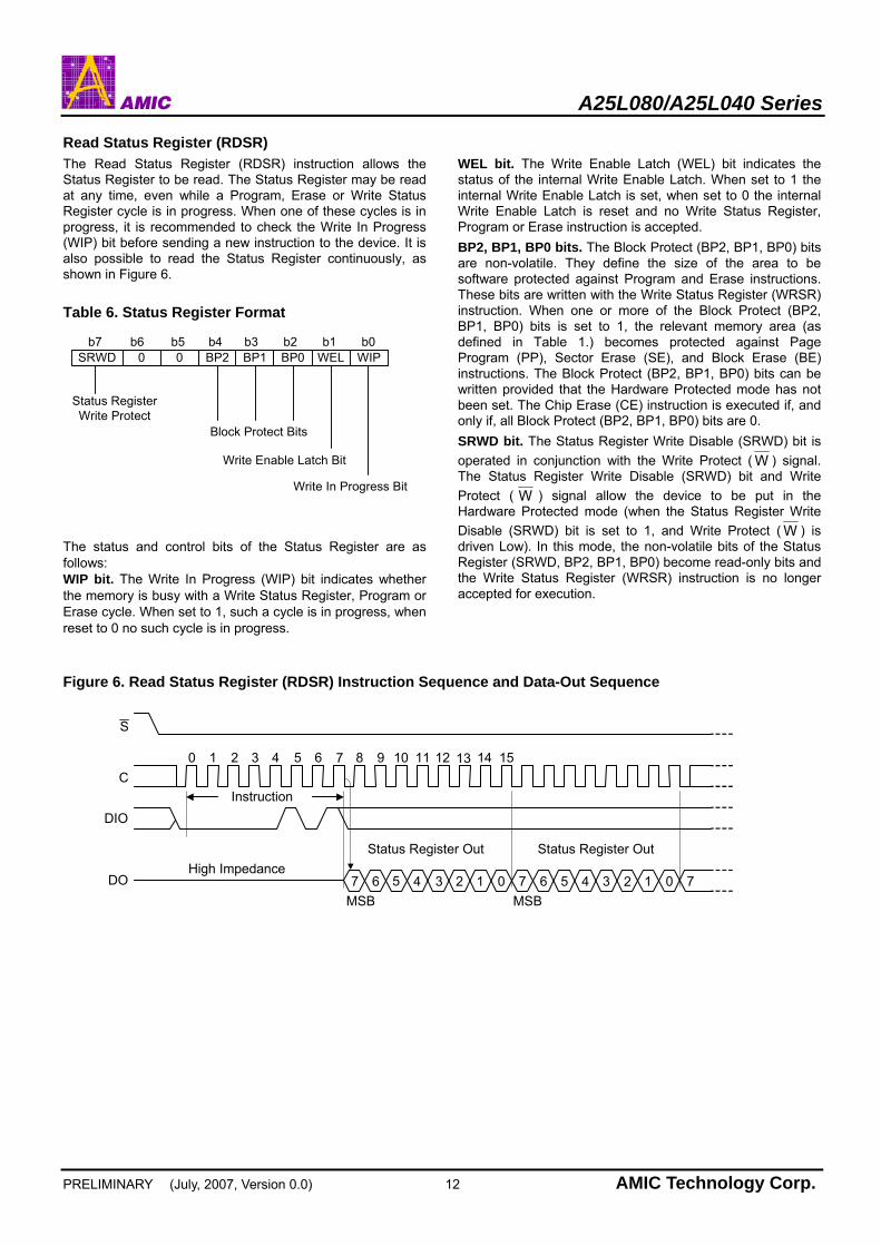
Read Status Register (RDSR) The Read Status Register (RDSR) instruction allows the Status Register to be read. The Status Register may be read at any time, even while a Program, Erase or Write Status Register cycle is in progress. When one of these cycles is in progress, it is recommended to check the Write In Progress (WIP) bit before sending a new instruction to the device. It is also possible to read the Status Register continuously, as shown in Figure 6.
Table 6. Status Register Format
SRWD 0 BP2 BP1 BP0 WEL WIP
Status RegisterWrite Protect
Block Protect Bits
Write Enable Latch Bit
Write In Progress Bit
b0b70
b6 b5 b4 b3 b2 b1
The status and control bits of the Status Register are as follows: WIP bit. The Write In Progress (WIP) bit indicates whether the memory is busy with a Write Status Register, Program or Erase cycle. When set to 1, such a cycle is in progress, when reset to 0 no such cycle is in progress.
WEL bit. The Write Enable Latch (WEL) bit indicates the status of the internal Write Enable Latch. When set to 1 the internal Write Enable Latch is set, when set to 0 the internal Write Enable Latch is reset and no Write Status Register, Program or Erase instruction is accepted. BP2, BP1, BP0 bits. The Block Protect (BP2, BP1, BP0) bits are non-volatile. They define the size of the area to be software protected against Program and Erase instructions. These bits are written with the Write Status Register (WRSR) instruction. When one or more of the Block Protect (BP2, BP1, BP0) bits is set to 1, the relevant memory area (as defined in Table 1.) becomes protected against Page Program (PP), Sector Erase (SE), and Block Erase (BE) instructions. The Block Protect (BP2, BP1, BP0) bits can be written provided that the Hardware Protected mode has not been set. The Chip Erase (CE) instruction is executed if, and only if, all Block Protect (BP2, BP1, BP0) bits are 0. SRWD bit. The Status Register Write Disable (SRWD) bit is operated in conjunction with the Write Protect ( W ) signal. The Status Register Write Disable (SRWD) bit and Write Protect ( W ) signal allow the device to be put in the Hardware Protected mode (when the Status Register Write Disable (SRWD) bit is set to 1, and Write Protect ( W ) is driven Low). In this mode, the non-volatile bits of the Status Register (SRWD, BP2, BP1, BP0) become read-only bits and the Write Status Register (WRSR) instruction is no longer accepted for execution.
Figure 6. Read Status Register (RDSR) Instruction Sequence and Data-Out Sequence
01234567
8 109 11 12 13 14 15
MSB MSB
Status Register OutStatus Register OutHigh Impedance
Instruction
0 1 2 3 4 5 6 7
01 234567 7
S
C
DIO
DO
A25L080/A25L040 Series
PRELIMINARY (July, 2007, Version 0.0) 13 AMIC Technology Corp.
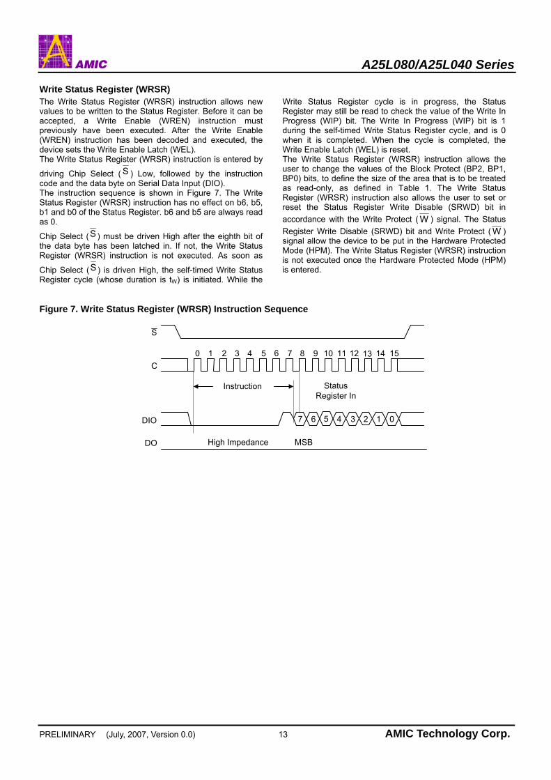
Write Status Register (WRSR) The Write Status Register (WRSR) instruction allows new values to be written to the Status Register. Before it can be accepted, a Write Enable (WREN) instruction must previously have been executed. After the Write Enable (WREN) instruction has been decoded and executed, the device sets the Write Enable Latch (WEL). The Write Status Register (WRSR) instruction is entered by
driving Chip Select ( S ) Low, followed by the instruction code and the data byte on Serial Data Input (DIO). The instruction sequence is shown in Figure 7. The Write Status Register (WRSR) instruction has no effect on b6, b5, b1 and b0 of the Status Register. b6 and b5 are always read as 0.
Chip Select (S ) must be driven High after the eighth bit of the data byte has been latched in. If not, the Write Status Register (WRSR) instruction is not executed. As soon as
Chip Select (S ) is driven High, the self-timed Write Status Register cycle (whose duration is tW) is initiated. While the
Write Status Register cycle is in progress, the Status Register may still be read to check the value of the Write In Progress (WIP) bit. The Write In Progress (WIP) bit is 1 during the self-timed Write Status Register cycle, and is 0 when it is completed. When the cycle is completed, the Write Enable Latch (WEL) is reset. The Write Status Register (WRSR) instruction allows the user to change the values of the Block Protect (BP2, BP1, BP0) bits, to define the size of the area that is to be treated as read-only, as defined in Table 1. The Write Status Register (WRSR) instruction also allows the user to set or reset the Status Register Write Disable (SRWD) bit in accordance with the Write Protect ( W ) signal. The Status Register Write Disable (SRWD) bit and Write Protect ( W ) signal allow the device to be put in the Hardware Protected Mode (HPM). The Write Status Register (WRSR) instruction is not executed once the Hardware Protected Mode (HPM) is entered.
Figure 7. Write Status Register (WRSR) Instruction Sequence
11 12 13 14 15
StatusRegister In
High Impedance
Instruction
S
C
DIO
DO MSB
8 1090 1 2 3 4 5 6 7
234567 01

A25L080/A25L040 Series
PRELIMINARY (July, 2007, Version 0.0) 14 AMIC Technology Corp.
Table 7. Protection Modes
Memory Content W Signal
SRWD Bit Mode Write Protection of the
Status Register Protected Area1 Unprotected Area1
1 0
0 0
1 1
Software Protected
(SPM)
Status Register is Writable (if the WREN instruction has set the WEL bit) The values in the SRWD, BP2, BP1, and BP0 bits can be changed
Protected against Page Program, Sector Erase, Block Erase, and Chip Erase
Ready to accept Page Program, Sector Erase, and Block Erase instructions
0 1 Hardware Protected
(HPM)
Status Register is Hardware write protected The values in the SRWD, BP2, BP1, and BP0 bits cannot be changed
Protected against Page Program, Sector Erase, Block Erase, and Chip Erase
Ready to accept Page Program, Sector Erase, and Block Erase instructions
Note: 1. As defined by the values in the Block Protect (BP2, BP1, BP0) bits of the Status Register, as shown in Table 1. The protection features of the device are summarized in Table 7. When the Status Register Write Disable (SRWD) bit of the Status Register is 0 (its initial delivery state), it is possible to write to the Status Register provided that the Write Enable Latch (WEL) bit has previously been set by a Write Enable (WREN) instruction, regardless of the whether Write Protect ( W ) is driven High or Low. When the Status Register Write Disable (SRWD) bit of the Status Register is set to 1, two cases need to be considered, depending on the state of Write Protect ( W ): If Write Protect ( W ) is driven High, it is possible to write
to the Status Register provided that the Write Enable Latch (WEL) bit has previously been set by a Write Enable (WREN) instruction.
If Write Protect (W) is driven Low, it is not possible to write to the Status Register even if the Write Enable Latch (WEL) bit has previously been set by a Write Enable (WREN) instruction. (Attempts to write to the Status
Register are rejected, and are not accepted for execution). As a consequence, all the data bytes in the memory area that are software protected (SPM) by the Block Protect (BP2, BP1, BP0) bits of the Status Register, are also hardware protected against data modification.
Regardless of the order of the two events, the Hardware Protected Mode (HPM) can be entered: by setting the Status Register Write Disable (SRWD) bit
after driving Write Protect ( W ) Low or by driving Write Protect ( W ) Low after setting the
Status Register Write Disable (SRWD) bit. The only way to exit the Hardware Protected Mode (HPM) once entered is to pull Write Protect ( W ) High.
If Write Protect ( W ) is permanently tied High, the Hardware Protected Mode (HPM) can never be activated, and only the Software Protected Mode (SPM), using the Block Protect (BP2, BP1, BP0) bits of the Status Register, can be used.
A25L080/A25L040 Series
PRELIMINARY (July, 2007, Version 0.0) 15 AMIC Technology Corp.
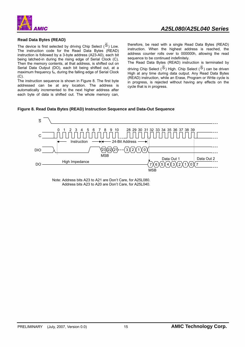
Read Data Bytes (READ) The device is first selected by driving Chip Select (S ) Low. The instruction code for the Read Data Bytes (READ) instruction is followed by a 3-byte address (A23-A0), each bit being latched-in during the rising edge of Serial Clock (C). Then the memory contents, at that address, is shifted out on Serial Data Output (DO), each bit being shifted out, at a maximum frequency fR, during the falling edge of Serial Clock (C). The instruction sequence is shown in Figure 8. The first byte addressed can be at any location. The address is automatically incremented to the next higher address after each byte of data is shifted out. The whole memory can,
therefore, be read with a single Read Data Bytes (READ) instruction. When the highest address is reached, the address counter rolls over to 000000h, allowing the read sequence to be continued indefinitely. The Read Data Bytes (READ) instruction is terminated by
driving Chip Select (S ) High. Chip Select (S ) can be driven High at any time during data output. Any Read Data Bytes (READ) instruction, while an Erase, Program or Write cycle is in progress, is rejected without having any effects on the cycle that is in progress.
Figure 8. Read Data Bytes (READ) Instruction Sequence and Data-Out Sequence
S
C
DIO
DO
Instruction
High ImpedanceMSB
MSB
8 1090 1 2 3 4 5 6 7
Data Out 1 Data Out 2
24-Bit Address
28 29 30 31 32 33 34 35 36 37 38 39
23 22 21 3 2 1 0
76 5 4 3 2 1 07
Note: Address bits A23 to A21 are Don’t Care, for A25L080.
Address bits A23 to A20 are Don’t Care, for A25L040.

A25L080/A25L040 Series
PRELIMINARY (July, 2007, Version 0.0) 16 AMIC Technology Corp.
Read Data Bytes at Higher Speed (FAST_READ)
The device is first selected by driving Chip Select (S ) Low. The instruction code for the Read Data Bytes at Higher Speed (FAST_READ) instruction is followed by a 3-byte address (A23-A0) and a dummy byte, each bit being latched-in during the rising edge of Serial Clock (C). Then the memory contents, at that address, is shifted out on Serial Data Output (DO), each bit being shifted out, at a maximum frequency fC, during the falling edge of Serial Clock (C). The instruction sequence is shown in Figure 9. The first byte addressed can be at any location. The address is automatically incremented to the next higher address after each byte of data is shifted out. The whole memory can, therefore, be read with a single Read Data Bytes at Higher
Speed (FAST_READ) instruction. When the highest address is reached, the address counter rolls over to 000000h, allowing the read sequence to be continued indefinitely. The Read Data Bytes at Higher Speed (FAST_READ)
instruction is terminated by driving Chip Select ( S ) High.
Chip Select (S ) can be driven High at any time during data output. Any Read Data Bytes at Higher Speed (FAST_READ) instruction, while an Erase, Program or Write cycle is in progress, is rejected without having any effects on the cycle that is in progress.
Figure 9. Read Data Bytes at Higher Speed (FAST_READ) Instruction Sequence and Data-Out Sequence
Instruction
High ImpedanceMSB
8 1090 1 2 3 4 5 6 7
24-Bit Address
28 29 30 31
23 22 21 3 2 1 0
Data Out 1 Data Out 2
7
0
S
C
DIO
DO
S
C
DIO
DO
32 33 34 35 36 37 38 39
6 5 4 17 3
40 41 42 43 44 45 46 47
2 0
Dummy Byte
MSB0
MSB7 6 5 4 3 2 1
MSB7 6 5 4 3 2 1 0
Note: Address bits A23 to A21 are Don’t Care, for A25L080.
Address bits A23 to A20 are Don’t Care, for A25L040.

A25L080/A25L040 Series
PRELIMINARY (July, 2007, Version 0.0) 17 AMIC Technology Corp.
Fast Read Dual Output (3Bh) The Fast Read Dual Output (3Bh) instruction is similar to the Fast_Read (0Bh) instruction except the data is output on two pins, DO and DIO, instead of just DO. This allows data to be transferred from the A25L080/A25L040 at twice the rate of standard SPI devices. Similar to the Fast Read instruction, the Fast Read Dual Output instruction can operate at the highest possible frequency of fC (See AC Characteristics). This is
accomplished by adding eight “dummy” clocks after the 24-bit address as shown in figure 10. The dummy clocks allow the device’s internal circuits additional time for setting up the initial address. The input data during the dummy clocks is “don’t care”. However, the DIO pin should be high-impedance prior to the falling edge of the first data out clock.
Figure 10. FAST_READ_DUAL_OUTPUT Instruction Sequence and Data-Out Sequence
Instruction
High ImpedanceMSB
8 1090 1 2 3 4 5 6 7
24-Bit Address
28 29 30 31
23 22 21 3 2 1 0
7
0
S
C
DIO
DO
S
C
DIO
DO
32 33 34 35 36 37 38 39
6 5 4 17 3
40 41 42 43 44 45 46 47
2 0
Dummy Byte
MSB1
MSB7 5 3 1 7 5 3
MSB7 5 3 1 7 5 3 1
6 4 2 0 6 4 2 0 6 4 2 0 6 4 2 0
Data Out 1 Data Out 2 Data Out 3 Data Out 4
DIO switches from input to output
Note: Address bits A23 to A21 are Don’t Care, for A25L080.
Address bits A23 to A20 are Don’t Care, for A25L040.

A25L080/A25L040 Series
PRELIMINARY (July, 2007, Version 0.0) 18 AMIC Technology Corp.
Fast Read Dual Input-Output (BBh) The Fast Read Dual Input-Output (BBh) instruction is similar to the Fast_Read (0Bh) instruction except the data is input and output on two pins, DO and DIO, instead of just DO. This allows data to be transferred from the A25L080/A25L040 at twice the rate of standard SPI devices. Similar to the Fast Read instruction, the Fast Read Dual Output instruction can operate at the highest possible frequency of fC (See AC Characteristics). This is
accomplished by adding four “dummy” clocks after the 24-bit address as shown in figure 11. The dummy clocks allow the device’s internal circuits additional time for setting up the initial address. The input data during the dummy clocks is “don’t care”. However, the DIO and DO pins should be high-impedance prior to the falling edge of the first data out clock.
Figure 11. FAST_READ_DUAL_INPUT-OUTPUT Instruction Sequence and Data-Out Sequence
Instruction
High ImpedanceMSB
8 1090 1 2 3 4 5 6 7
24-Bit Address
16 17 18 19
22 20 18 6 4 2 0
7
0
S
C
DIO
DO
S
C
DIO
DO
20 21 22 23 24 25 26 27 28 29 30 31 32 33 34 35
DummyByte
MSB1
MSB7 5 3 1 7 5 3
MSB7 5 3 1 7 5 3 1
6 4 2 0 6 4 2 0 6 4 2 0 6 4 2 0
Data Out 2 Data Out 3 Data Out 4 Data Out 5
DIO switches from input to output
21 19 5 3 123 7
6 4 2 03 2 1 0
7 5 3 1MSB
Data Out 1
Note: Address bits A23 to A21 are Don’t Care, for A25L080. Address bits A23 to A20 are Don’t Care, for A25L040.

A25L080/A25L040 Series
PRELIMINARY (July, 2007, Version 0.0) 19 AMIC Technology Corp.
Page Program (PP) The Page Program (PP) instruction allows bytes to be programmed in the memory (changing bits from 1 to 0). Before it can be accepted, a Write Enable (WREN) instruction must previously have been executed. After the Write Enable (WREN) instruction has been decoded, the device sets the Write Enable Latch (WEL). The Page Program (PP) instruction is entered by driving Chip
Select ( S ) Low, followed by the instruction code, three address bytes and at least one data byte on Serial Data Input (DIO). If the 8 least significant address bits (A7-A0) are not all zero, all transmitted data that goes beyond the end of the current page are programmed from the start address of the same page (from the address whose 8 least significant bits
(A7-A0) are all zero). Chip Select (S ) must be driven Low for the entire duration of the sequence. The instruction sequence is shown in Figure 12. If more than 256 bytes are sent to the device, previously latched data are discarded and the last 256 data bytes are guaranteed to be
programmed correctly within the same page. If less than 256 Data bytes are sent to device, they are correctly programmed at the requested addresses without having any effects on the other bytes of the same page.
Chip Select (S ) must be driven High after the eighth bit of the last data byte has been latched in, otherwise the Page Program (PP) instruction is not executed.
As soon as Chip Select ( S ) is driven High, the self-timed Page Program cycle (whose duration is tPP) is initiated. While the Page Program cycle is in progress, the Status Register may be read to check the value of the Write In Progress (WIP) bit. The Write In Progress (WIP) bit is 1 during the self-timed Page Program cycle, and is 0 when it is completed. At some unspecified time before the cycle is completed, the Write Enable Latch (WEL) bit is reset. A Page Program (PP) instruction applied to a page which is protected by the Block Protect (BP2, BP1, BP0) bits (see Table 1. and Table 2.) is not executed.
Figure 12. Page Program (PP) Instruction Sequence
S
C
DIO
Instruction
MSB
8 1090 1 2 3 4 5 6 7
24-Bit Address
28 29 30 31 32 33 34 35 36 37 38 39
23 22 21 3 2 1 0
Data Byte 1
MSB7 6 5 4 3 2 1 03
Data Byte 256
5553 5452
Data Byte 3
515049484746454443424140
Data Byte 2
0MSB7 6 5 4 3 2 1
MSB7 6 5 4 3 2 1 0
MSB7 6 5 4 3 2 1 0
S
C
DIO
2072
2073
2074
2075
2076
2077
2078
2079
Note: Address bits A23 to A21 are Don’t Care, for A25L080.
Address bits A23 to A20 are Don’t Care, for A25L040.

A25L080/A25L040 Series
PRELIMINARY (July, 2007, Version 0.0) 20 AMIC Technology Corp.
Sector Erase (SE) The Sector Erase (SE) instruction sets to 1 (FFh) all bits inside the chosen sector. Before it can be accepted, a Write Enable (WREN) instruction must previously have been ex-ecuted. After the Write Enable (WREN) instruction has been decoded, the device sets the Write Enable Latch (WEL). The Sector Erase (SE) instruction is entered by driving Chip
Select (S ) Low, followed by the instruction code on Serial
Data Input (DIO). Chip Select (S ) must be driven Low for the entire duration of the sequence. The instruction sequence is shown in Figure 13. Chip Select
(S ) must be driven High after the eighth bit of the instruction code has been latched in, otherwise the Sector Erase
instruction is not executed. As soon as Chip Select (S ) is driven High, the self-timed Sector Erase cycle (whose duration is tSE) is initiated. While the Sector Erase cycle is in progress, the Status Register may be read to check the value of the Write In Progress (WIP) bit. The Write In Progress (WIP) bit is 1 during the self-timed Sector Erase cycle, and is 0 when it is completed. At some unspecified time before the cycle is completed, the Write Enable Latch (WEL) bit is reset. A Sector Erase (SE) instruction applied to a page which is protected by the Block Protect (BP2, BP1, BP0) bits (see table 1. and table 2.) is not executed.
Figure 13. Sector Erase (SE) Instruction Sequence
Instruction
MSB
8 1090 1 2 3 4 5 6 7
24-Bit Address
28 29 30 31
23
S
C
DIO 22 21 3 2 1 0023
Note: Address bits A23 to A21 are Don’t Care, for A25L080. Address bits A23 to A20 are Don’t Care, for A25L040.
A25L080/A25L040 Series
PRELIMINARY (July, 2007, Version 0.0) 21 AMIC Technology Corp.
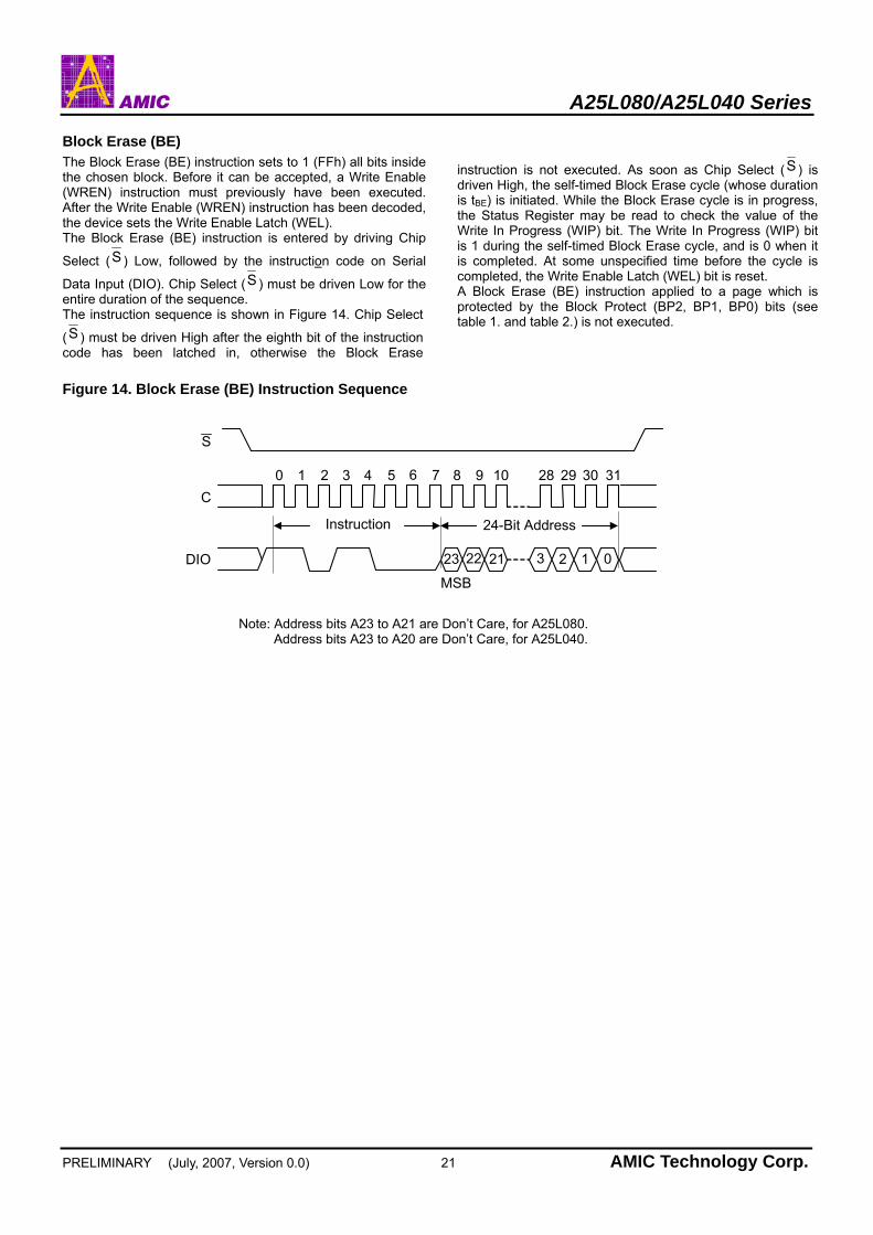
Block Erase (BE) The Block Erase (BE) instruction sets to 1 (FFh) all bits inside the chosen block. Before it can be accepted, a Write Enable (WREN) instruction must previously have been executed. After the Write Enable (WREN) instruction has been decoded, the device sets the Write Enable Latch (WEL). The Block Erase (BE) instruction is entered by driving Chip
Select (S ) Low, followed by the instruction code on Serial
Data Input (DIO). Chip Select (S ) must be driven Low for the entire duration of the sequence. The instruction sequence is shown in Figure 14. Chip Select
(S ) must be driven High after the eighth bit of the instruction code has been latched in, otherwise the Block Erase
instruction is not executed. As soon as Chip Select (S ) is driven High, the self-timed Block Erase cycle (whose duration is tBE) is initiated. While the Block Erase cycle is in progress, the Status Register may be read to check the value of the Write In Progress (WIP) bit. The Write In Progress (WIP) bit is 1 during the self-timed Block Erase cycle, and is 0 when it is completed. At some unspecified time before the cycle is completed, the Write Enable Latch (WEL) bit is reset. A Block Erase (BE) instruction applied to a page which is protected by the Block Protect (BP2, BP1, BP0) bits (see table 1. and table 2.) is not executed.
Figure 14. Block Erase (BE) Instruction Sequence
Instruction
MSB
8 1090 1 2 3 4 5 6 7
24-Bit Address
28 29 30 31
23
S
C
DIO 22 21 3 2 1 0023
Note: Address bits A23 to A21 are Don’t Care, for A25L080. Address bits A23 to A20 are Don’t Care, for A25L040.

A25L080/A25L040 Series
PRELIMINARY (July, 2007, Version 0.0) 22 AMIC Technology Corp.
Chip Erase (CE) The Chip Erase (CE) instruction sets all bits to 1 (FFh). Before it can be accepted, a Write Enable (WREN) instruction must previously have been executed. After the Write Enable (WREN) instruction has been decoded, the device sets the Write Enable Latch (WEL). The Chip Erase (CE) instruction is entered by driving Chip
Select (S ) Low, followed by the instruction code on Serial
Data Input (DIO). Chip Select (S ) must be driven Low for the entire duration of the sequence. The instruction sequence is shown in Figure 15. Chip Select
(S ) must be driven High after the eighth bit of the instruction code has been latched in, otherwise the Bulk Erase instruction
is not executed. As soon as Chip Select (S ) is driven High, the self-timed Chip Erase cycle (whose duration is tCE) is initiated. While the Chip Erase cycle is in progress, the Status Register may be read to check the value of the Write In Progress (WIP) bit. The Write In Progress (WIP) bit is 1 during the self-timed Chip Erase cycle, and is 0 when it is completed. At some unspecified time before the cycle is completed, the Write Enable Latch (WEL) bit is reset. The Chip Erase (CE) instruction is executed only if all Block Protect (BP2, BP1, BP0) bits are 0. The Chip Erase (CE) instruction is ignored if one, or more, blocks are protected.
Figure 15. Chip Erase (CE) Instruction Sequence
S
C
DIO
1 2 3 4 5 6 70
Instruction
Note: Address bits A23 to A21 are Don’t Care, for A25L080. Address bits A23 to A20 are Don’t Care, for A25L040.

A25L080/A25L040 Series
PRELIMINARY (July, 2007, Version 0.0) 23 AMIC Technology Corp.
Deep Power-down (DP) Executing the Deep Power-down (DP) instruction is the only way to put the device in the lowest consumption mode (the Deep Power-down mode). It can also be used as an extra software protection mechanism, while the device is not in active use, since in this mode, the device ignores all Write, Program and Erase instructions.
Driving Chip Select (S ) High deselects the device, and puts the device in the Standby mode (if there is no internal cycle currently in progress). But this mode is not the Deep Power-down mode. The Deep Power-down mode can only be entered by executing the Deep Power-down (DP) instruction, to reduce the standby current (from ICC1 to ICC2, as specified in DC Characteristics Table.). Once the device has entered the Deep Power-down mode, all instructions are ignored except the Release from Deep Power-down and Read Electronic Signature (RES) instruction. This releases the device from this mode. The Release from Deep Power-down and Read Electronic Signature (RES) instruction also allows the Electronic Signature of the device to be output on Serial Data Output (DO).
The Deep Power-down mode automatically stops at Power-down, and the device always Powers-up in the Standby mode. The Deep Power-down (DP) instruction is entered by driving
Chip Select ( S ) Low, followed by the instruction code on
Serial Data Input (DIO). Chip Select (S ) must be driven Low for the entire duration of the sequence. The instruction sequence is shown in Figure 16.
Chip Select (S ) must be driven High after the eighth bit of the instruction code has been latched in, otherwise the Deep Power-down (DP) instruction is not executed. As soon as
Chip Select ( S ) is driven High, it requires a delay of tDP before the supply current is reduced to ICC2 and the Deep Power-down mode is entered. Any Deep Power-down (DP) instruction, while an Erase, Program or Write cycle is in progress, is rejected without having any effects on the cycle that is in progress.
Figure 16. Deep Power-down (DP) Instruction Sequence
S
C
DIO
1 2 3 4 5 6 70
Instruction
tDP
Stand-by Mode Deep Power-down Mode
A25L080/A25L040 Series
PRELIMINARY (July, 2007, Version 0.0) 24 AMIC Technology Corp.
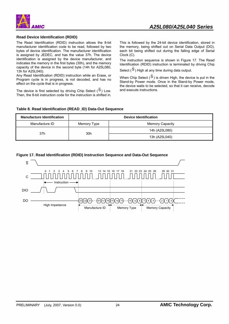
Read Device Identification (RDID) The Read Identification (RDID) instruction allows the 8-bit manufacturer identification code to be read, followed by two bytes of device identification. The manufacturer identification is assigned by JEDEC, and has the value 37h. The device identification is assigned by the device manufacturer, and indicates the memory in the first bytes (30h), and the memory capacity of the device in the second byte (14h for A25L080, 13h for A25L040). Any Read Identification (RDID) instruction while an Erase, or Program cycle is in progress, is not decoded, and has no effect on the cycle that is in progress.
The device is first selected by driving Chip Select (S ) Low. Then, the 8-bit instruction code for the instruction is shifted in.
This is followed by the 24-bit device identification, stored in the memory, being shifted out on Serial Data Output (DO), each bit being shifted out during the falling edge of Serial Clock (C). The instruction sequence is shown in Figure 17. The Read Identification (RDID) instruction is terminated by driving Chip
Select (S ) High at any time during data output.
When Chip Select (S ) is driven High, the device is put in the Stand-by Power mode. Once in the Stand-by Power mode, the device waits to be selected, so that it can receive, decode and execute instructions.
Table 8. Read Identification (READ_ID) Data-Out Sequence
Manufacture Identification Device Identification
Manufacture ID Memory Type Memory Capacity
14h (A25L080) 37h 30h
13h (A25L040)
Figure 17. Read Identification (RDID) Instruction Sequence and Data-Out Sequence
S
C
DIO
DO
Instruction
High Impedance
8 1090 1 2 3 4 5 6 7 21 3022 23 24 25 26 29 31
Manufacture ID Memory Type
7 6 5 2 1 015 14 13 10 9 823 22 21 18 17 16
13 1514 16 17 18
Memory Capacity

A25L080/A25L040 Series
PRELIMINARY (July, 2007, Version 0.0) 25 AMIC Technology Corp.
Read Electronic Manufacturer ID & Device ID (REMS) The Read Electronic Manufacturer ID & Device ID (REMS) instruction allows the 8-bit manufacturer identification code to be read, followed by one byte of device identification. The manufacturer identification is assigned by JEDEC, and has the value 37h for AMIC. The device identification is assigned by the device manufacturer, and has the value 13h for A25L080, 12h for A25L040. Any Read Electronic Manufacturer ID & Device ID (REMS) instruction while an Erase, or Program cycle is in progress, is not decoded, and has no effect on the cycle that is in progress.
The device is first selected by driving Chip Select (S ) Low. The 8-bit instruction code is followd by 2 dummy bytes and one byte address(A7~A0), each bit being latched-in on Serial Data Input (DIO) during the rising edge of Serial Clock (C).
If the one-byte address is set to 01h, then the device ID will be read first and then followed by the Manufacturer ID. On the other hand, if the one-byte address is set to 00h, then the Manufacturer ID will be read first and then followed by the device ID. The instruction sequence is shown in Figure 18. The Read Electronic Manufacturer ID & Device ID (REMS) instruction is
terminated by driving Chip Select (S ) High at any time during data output. When Chip Select (S ) is driven High, the device is put in the Stand-by Power mode. Once in the Stand-by Power mode, the device waits to be selected, so that it can receive, decode and execute instructions.
Table 8. Read Electronic Manufacturer ID & Device ID (REMS) Data-Out Sequence
Manufacture Identification Device Identification
13h (A25L080) 37h
12h (A25L040)
Figure 18. Read Electronic Manufacturer ID & Device ID (REMS) Instruction Sequence and Data-Out Sequence
Instruction
High ImpedanceMSB
8 1090 1 2 3 4 5 6 7
2 Dummy Bytes
20 21 22 23
15 14 13 3 2 1 0
Manufacturer ID
0
S
C
DIO
DO
S
C
DIO
DO
24 25 26 27 28 29 30 31
6 5 4 17 3
32 33 34 35 36 37 38 39
2 0
ADD(1)
MSB0
MSB7 6 5 4 3 2 1
MSB7 6 5 4 3 2 1 0
40 41 42 43 44 45 46 47
Device ID
Notes:(1) ADD=00h will output the manufacturer ID first and ADD=01h will output device ID first

A25L080/A25L040 Series
PRELIMINARY (July, 2007, Version 0.0) 26 AMIC Technology Corp.
Release from Deep Power-down and Read Electronic Signature (RES) Once the device has entered the Deep Power-down mode, all instructions are ignored except the Release from Deep Power-down and Read Electronic Signature (RES) instruction. Executing this instruction takes the device out of the Deep Power-down mode. The instruction can also be used to read, on Serial Data Output (DO), the 8-bit Electronic Signature, whose value for the A25L08 is 13h, and for A25L040 is 12h. Except while an Erase, Program or Write Status Register cycle is in progress, the Release from Deep Power-down and Read Electronic Signature (RES) instruction always provides access to the 8-bit Electronic Signature of the device, and can be applied even if the Deep Power-down mode has not been entered. Any Release from Deep Power-down and Read Electronic Signature (RES) instruction while an Erase, Program or Write Status Register cycle is in progress, is not decoded, and has no effect on the cycle that is in progress.
The device is first selected by driving Chip Select (S ) Low. The instruction code is followed by 3 dummy bytes, each bit being latched-in on Serial Data Input (DIO) during the rising
edge of Serial Clock (C). Then, the 8-bit Electronic Signature, stored in the memory, is shifted out on Serial Data Output (DO), each bit being shifted out during the falling edge of Serial Clock (C). The instruction sequence is shown in Figure 19. The Release from Deep Power-down and Read Electronic Signature (RES) instruction is terminated by driving Chip
Select (S ) High after the Electronic Signature has been read at least once. Sending additional clock cycles on Serial Clock
(C), while Chip Select ( S ) is driven Low, cause the Electronic Signature to be output repeatedly.
When Chip Select (S ) is driven High, the device is put in the Stand-by Power mode. If the device was not previously in the Deep Power-down mode, the transition to the Stand-by Power mode is immediate. If the device was previously in the Deep Power-down mode, though, the transition to the Stand-
by Power mode is delayed by tRES2, and Chip Select (S ) must remain High for at least tRES2 (max), as specified in AC Characteristics Table . Once in the Stand-by Power mode, the device waits to be selected, so that it can receive, decode and execute instructions.
Figure 19. Release from Deep Power-down and Read Electronic Signature (RES) Instruction Sequence and Data-Out Sequence
S
C
DIO
DO
Instruction
High ImpedanceMSB
MSB
8 1090 1 2 3 4 5 6 7
3 Dummy Bytes
28 29 30 31 32 33 34 35 36 37 38
23 22 21 3 2 1 0
6 5 4 3 2 1 07
tRES2
Stand-by ModeDeep Power-down Mode Note: The value of the 8-bit Electronic Signature, for the A25L080 is 13h, A25L040 is 12h.
A25L080/A25L040 Series
PRELIMINARY (July, 2007, Version 0.0) 27 AMIC Technology Corp.
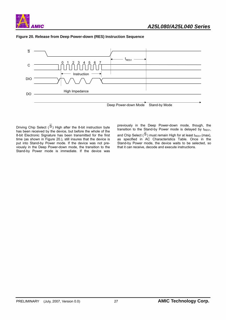
Figure 20. Release from Deep Power-down (RES) Instruction Sequence
S
C
DIO
1 2 3 4 5 6 70
Instruction
tRES1
High ImpedanceDO
Stand-by ModeDeep Power-down Mode
Driving Chip Select (S ) High after the 8-bit instruction byte has been received by the device, but before the whole of the 8-bit Electronic Signature has been transmitted for the first time (as shown in Figure 20.), still insures that the device is put into Stand-by Power mode. If the device was not pre-viously in the Deep Power-down mode, the transition to the Stand-by Power mode is immediate. If the device was
previously in the Deep Power-down mode, though, the transition to the Stand-by Power mode is delayed by tRES1,
and Chip Select (S ) must remain High for at least tRES1 (max), as specified in AC Characteristics Table. Once in the Stand-by Power mode, the device waits to be selected, so that it can receive, decode and execute instructions.

A25L080/A25L040 Series
PRELIMINARY (July, 2007, Version 0.0) 28 AMIC Technology Corp.
POWER-UP AND POWER-DOWN At Power-up and Power-down, the device must not be
selected (that is Chip Select ( S ) must follow the voltage applied on VCC) until VCC reaches the correct value: VCC (min) at Power-up, and then for a further delay of tVSL VSS at Power-down
Usually a simple pull-up resistor on Chip Select (S ) can be used to insure safe and proper Power-up and Power-down. To avoid data corruption and inadvertent write operations during power up, a Power On Reset (POR) circuit is included. The logic inside the device is held reset while VCC is less than the POR threshold value, VWI – all operations are disabled, and the device does not respond to any instruction. Moreover, the device ignores all Write Enable (WREN), Page Program (PP), Sector Erase (SE), Bulk Erase (BE) and Write Status Register (WRSR) instructions until a time delay of tPUW has elapsed after the moment that VCC rises above the VWI threshold. However, the correct operation of the device is not guaranteed if, by this time, VCC is still below VCC(min). No Write Status Register, Program or Erase instructions should be sent until the later of:
tPUW after VCC passed the VWI threshold - tVSL afterVCC passed the VCC(min) level These values are specified in Table 9. If the delay, tVSL, has elapsed, after VCC has risen above VCC(min), the device can be selected for READ instructions even if the tPUW delay is not yet fully elapsed. At Power-up, the device is in the following state: The device is in the Standby mode (not the Deep
Power-down mode). The Write Enable Latch (WEL) bit is reset. Normal precautions must be taken for supply rail decoupling, to stabilize the VCC feed. Each device in a system should have the VCC rail decoupled by a suitable capacitor close to the package pins. (Generally, this capacitor is of the order of 0.1µF). At Power-down, when VCC drops from the operating voltage, to below the POR threshold value, VWI, all operations are disabled and the device does not respond to any instruction. (The designer needs to be aware that if a Power-down occurs while a Write, Program or Erase cycle is in progress, some data corruption can result.)
Figure 21. Power-up Timing
time
VCC
VCC(max)
VCC(min)
tPU Full Device Access
A25L080/A25L040 Series
PRELIMINARY (July, 2007, Version 0.0) 29 AMIC Technology Corp.
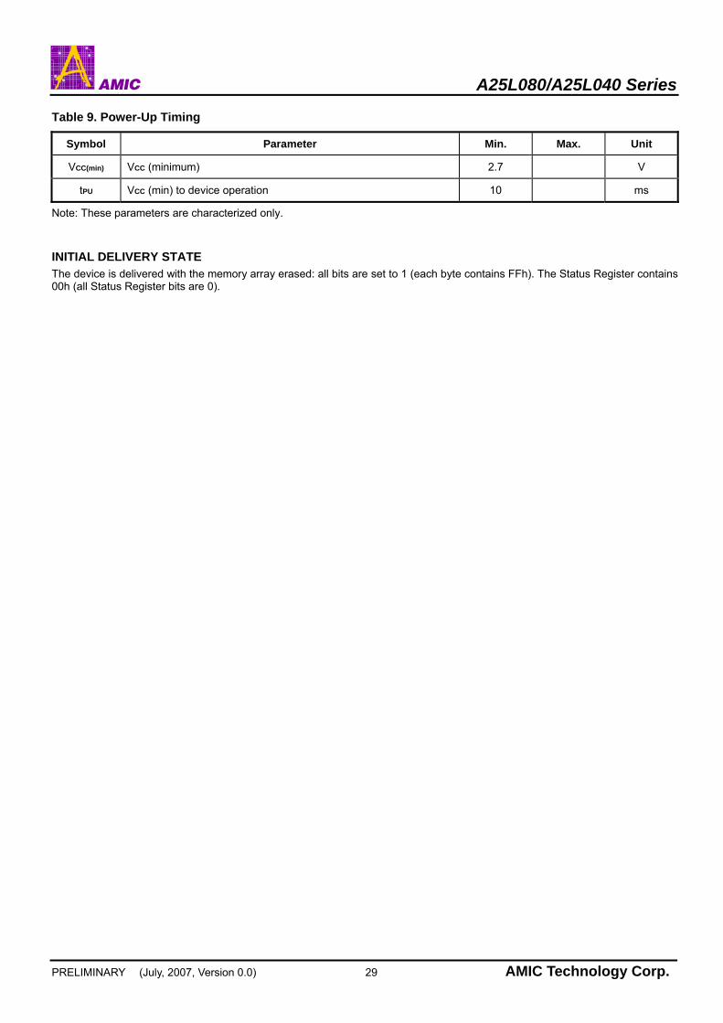
Table 9. Power-Up Timing
Symbol Parameter Min. Max. Unit
VCC(min) VCC (minimum) 2.7 V
tPU VCC (min) to device operation 10 ms
Note: These parameters are characterized only. INITIAL DELIVERY STATE The device is delivered with the memory array erased: all bits are set to 1 (each byte contains FFh). The Status Register contains 00h (all Status Register bits are 0).

A25L080/A25L040 Series
PRELIMINARY (July, 2007, Version 0.0) 30 AMIC Technology Corp.
Absolute Maximum Ratings* Storage Temperature (TSTG) . . . . . . . . . . -65°C to + 150°C Lead Temperature during Soldering (Note 1) D.C. Voltage on Any Pin to Ground Potential . . . . . . . . . . . . . . . . . . . . . . . . . . . . . . . . . . . . . . . . . . . -0.6V to VCC+0.6V Transient Voltage (<20ns) on Any Pin to Ground Potential . . . . . . . . . . . . . . . . . . . . . . . . . . . . . . . . . -2.0V to VCC+2.0V Supply Voltage (VCC) . . . . . . . . . . . . . . . . . . -0.6V to +4.0V Electrostatic Discharge Voltage (Human Body model) (VESD) (Note 2) . . . . . . . . . . . . . . . . . . . -2000V to 2000V Notes: 1. Compliant with JEDEC Std J-STD-020B (for small body,
Sn-Pb or Pb assembly). 2. JEDEC Std JESD22-A114A (C1=100 pF, R1=1500Ω ,
R2=500Ω)
*Comments Stressing the device above the rating listed in the Absolute Maximum Ratings" table may cause permanent damage to the device. These are stress ratings only and operation of the device at these or any other conditions above those indicated in the Operating sections of this specification is not implied. Exposure to Absolute Maximum Rating conditions for extended periods may affect device reliability. Refer also to the AMIC SURE Program and other relevant quality docu-ments.
DC AND AC PARAMETERS This section summarizes the operating and measurement conditions, and the DC and AC characteristics of the device. The parameters in the DC and AC Characteristic tables that follow are derived from tests performed under the
Measurement Conditions summarized in the relevant tables. Designers should check that the operating conditions in their circuit match the measurement conditions when relying on the quoted parameters.
Table 10. Operating Conditions
Symbol Parameter Min. Max. Unit
VCC Supply Voltage 2.7 3.6 V
TA Ambient Operating Temperature –40 85 °C
Table 11. Data Retention and Endurance
Parameter Condition Min. Max. Unit
Erase/Program Cycles At 85°C 100,000 Cycles per Sector
Data Retention At 85°C 20 Years
Note: 1. This is preliminary data Table 12. Capacitance
Symbol Parameter Test Condition Min. Max. Unit
COUT Output Capacitance (DO) VOUT = 0V 8 pF
CIN Input Capacitance (other pins) VIN = 0V 6 pF
Note: Sampled only, not 100% tested, at TA=25°C and a frequency of 33 MHz.

A25L080/A25L040 Series
PRELIMINARY (July, 2007, Version 0.0) 31 AMIC Technology Corp.
Table 13. DC Characteristics
Symbol Parameter Test Condition Min. Max. Unit
ILI Input Leakage Current ± 2 µA
ILO Output Leakage Current ± 2 µA
ICC1 Standby Current S = VCC, VIN = VSS or VCC 50 µA
ICC2 Deep Power-down Current S = VCC, VIN = VSS or VCC 10 µA
C= 0.1VCC / 0.9.VCC at 50MHz, DO = open 20 mA ICC3 Operating Current (READ)
C= 0.1VCC / 0.9.VCC at 33MHz, DO = open 15 mA
ICC4 Operating Current (PP) S = VCC 15 mA
ICC5 Operating Current (WRSR) S = VCC 15 mA
ICC6 Operating Current (SE) S = VCC 15 mA
ICC7 Operating Current (BE) S = VCC 15 mA
VIL Input Low Voltage –0.5 0.3VCC V
VIH Input High Voltage 0.7VCC VCC+0.4 V
VOL Output Low Voltage IOL = 1.6mA 0.4 V
VOH Output High Voltage IOH = –100µA VCC–0.2 V
Note: 1. This is preliminary data at 85°C Table 14. Instruction Times
Symbol Alt. Parameter Min. Typ. Max. Unit
tW Write Status Register Cycle Time 100 300 ms
tPP Page Program Cycle Time 3 5 ms
tSE Sector Erase Cycle Time 0.5 1 s
tBE Block Erase Cycle Time 1 3 s
Chip Erase Cycle Time of A25L080 10 40 s tCE
Chip Erase Cycle Time of A25L040 5 20 s
Note: 1. At 85°C 2. This is preliminary data
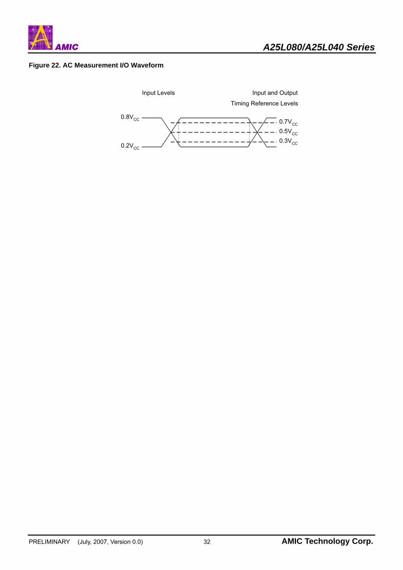
Table 15. AC Measurement Conditions
Symbol Parameter Min. Max. Unit
CL Load Capacitance 30 pF
Input Rise and Fall Times 5 ns
Input Pulse Voltages 0.2VCC to 0.8VCC V
Input Timing Reference Voltages 0.3VCC to 0.7VCC V
Output Timing Reference Voltages VCC / 2 V
Note: Output Hi-Z is defined as the point where data out is no longer driven.
A25L080/A25L040 Series
PRELIMINARY (July, 2007, Version 0.0) 32 AMIC Technology Corp.
Figure 22. AC Measurement I/O Waveform
0.3VCC
0.5VCC
0.2VCC
0.7VCC
0.8VCC
Input Levels Input and Output
Timing Reference Levels
A25L080/A25L040 Series
PRELIMINARY (July, 2007, Version 0.0) 33 AMIC Technology Corp.
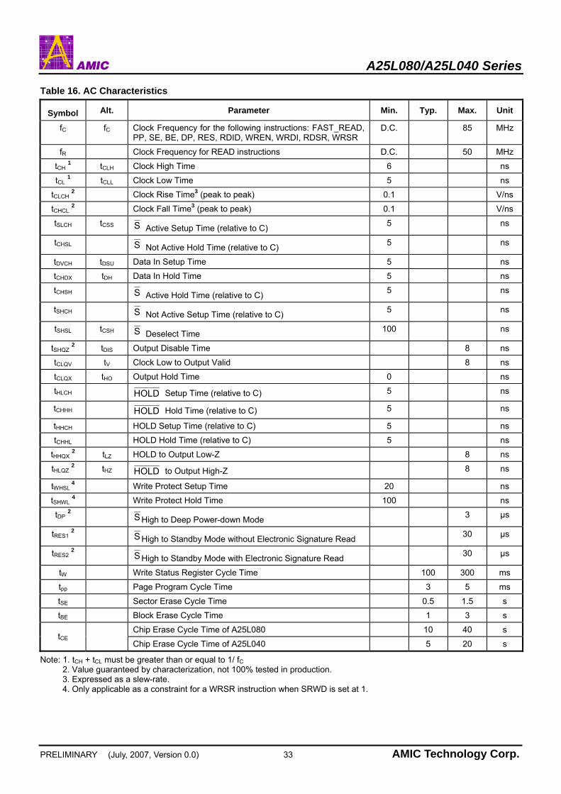
Table 16. AC Characteristics
Symbol Alt. Parameter Min. Typ. Max. Unit
fC fC Clock Frequency for the following instructions: FAST_READ, PP, SE, BE, DP, RES, RDID, WREN, WRDI, RDSR, WRSR
D.C. 85 MHz
fR Clock Frequency for READ instructions D.C. 50 MHz
tCH 1 tCLH Clock High Time 6 ns
tCL 1 tCLL Clock Low Time 5 ns tCLCH 2 Clock Rise Time3 (peak to peak) 0.1 V/ns
tCHCL 2 Clock Fall Time3 (peak to peak) 0.1 V/ns
tSLCH tCSS S Active Setup Time (relative to C) 5 ns
tCHSL S Not Active Hold Time (relative to C) 5 ns
tDVCH tDSU Data In Setup Time 5 ns
tCHDX tDH Data In Hold Time 5 ns
tCHSH S Active Hold Time (relative to C) 5 ns
tSHCH S Not Active Setup Time (relative to C) 5 ns
tSHSL tCSH S Deselect Time 100 ns
tSHQZ 2 tDIS Output Disable Time 8 ns
tCLQV tV Clock Low to Output Valid 8 ns
tCLQX tHO Output Hold Time 0 ns
tHLCH HOLD Setup Time (relative to C) 5 ns
tCHHH HOLD Hold Time (relative to C) 5 ns
tHHCH HOLD Setup Time (relative to C) 5 ns
tCHHL HOLD Hold Time (relative to C) 5 ns
tHHQX 2 tLZ HOLD to Output Low-Z 8 ns
tHLQZ 2 tHZ HOLD to Output High-Z 8 ns
tWHSL 4 Write Protect Setup Time 20 ns
tSHWL 4 Write Protect Hold Time 100 ns
tDP 2 SHigh to Deep Power-down Mode 3 µs
tRES1 2 SHigh to Standby Mode without Electronic Signature Read 30 µs
tRES2 2 SHigh to Standby Mode with Electronic Signature Read 30 µs
tW Write Status Register Cycle Time 100 300 ms
tpp Page Program Cycle Time 3 5 ms
tSE Sector Erase Cycle Time 0.5 1.5 s
tBE Block Erase Cycle Time 1 3 s
Chip Erase Cycle Time of A25L080 10 40 s tCE
Chip Erase Cycle Time of A25L040 5 20 s
Note: 1. tCH + tCL must be greater than or equal to 1/ fC 2. Value guaranteed by characterization, not 100% tested in production. 3. Expressed as a slew-rate. 4. Only applicable as a constraint for a WRSR instruction when SRWD is set at 1.

A25L080/A25L040 Series
PRELIMINARY (July, 2007, Version 0.0) 34 AMIC Technology Corp.
Figure 23. Serial Input Timing
S
C
DIO
tSHSL
High ImpedanceDO
tSLCHtCHSL tSHCH
tCHDX
tCHSH
tDVCHtCLCH
LSB INMSB IN
tCHCL
Figure 24. Write Protect Setup and Hold Timing during WRSR when SRWD=1
High Impedance
tWHSL tSHWL
S
C
DIO
DO
W

A25L080/A25L040 Series
PRELIMINARY (July, 2007, Version 0.0) 35 AMIC Technology Corp.
Figure 25. Hold Timing
S
C
DO
DIO
HOLD
tHLQZ
tHLCHtHHCHtCHHL
tCHHH
tHHQX
Figure 26. Output Timing
S
C
DO
DIO ADDR.LSB IN
LSB OUT
tCLQVtCLQV
tCH
tCLQXtCLQX
tCL
tQLQHtQHQL
tSHQZ

A25L080/A25L040 Series
PRELIMINARY (July, 2007, Version 0.0) 36 AMIC Technology Corp.
Part Numbering Scheme
Package Type M = 209 mil SOP 8 O = 150 mil SOP 8 Blank = DIP8
Device Voltage L = 2.7-3.6V
Device Version*
Device TypeA25 = AMIC Serial Flash
Device Density 512 = 512 Kbit (4KB uniform sectors) 010 = 1 Mbit (4KB uniform sectors) 020 = 2 Mbit (4KB uniform sectors) 040 = 4 Mbit (4KB uniform sectors) 080 = 8 Mbit (4KB uniform sectors) 016 = 16 Mbit (4KB uniform sectors) 032 = 32 Mbit (4KB uniform sectors)
Temperature*
Package Material Blank: normal F: PB free
* Optional

A25L080/A25L040 Series
PRELIMINARY (July, 2007, Version 0.0) 37 AMIC Technology Corp.
Ordering Information
Part No. Speed (MHz) Active Read Current
Typ. (mA)
Program/Erase Current
Typ. (mA)
Standby Current Typ. (μA)
Package
A25L080-F
A25L080-UF
8 Pin Pb-Free DIP (300 mil)
8 Pin Pb-Free DIP (300 mil)
A25L080O-F
A25L080O-UF
8 Pb-Free Pin SOP (150mil)
8 Pb-Free Pin SOP (150mil)
A25L080M-F
A25L080M-UF
85 20 15 50
8 Pb-Free Pin SOP (209mil)
8 Pb-Free Pin SOP (209mil)
-U is for industrial operating temperature range: -40°C ~ +85°C
Part No. Speed (MHz) Active Read Current
Typ. (mA)
Program/Erase Current
Typ. (mA)
Standby Current Typ. (μA)
Package
A25L040-F
A25L040-UF
8 Pin Pb-Free DIP (300 mil)
8 Pin Pb-Free DIP (300 mil)
A25L040O-F
A25L040O-UF
8 Pin Pb-Free SOP (150 mil)
8 Pin Pb-Free SOP (150 mil)
A25L040M-F
A25L040M-UF
85 20 15 50
8 Pb-Free Pin SOP (209mil)
8 Pb-Free Pin SOP (209mil)
-U is for industrial operating temperature range: -40°C ~ +85°C
A25L080/A25L040 Series
PRELIMINARY (July, 2007, Version 0.0) 38 AMIC Technology Corp.
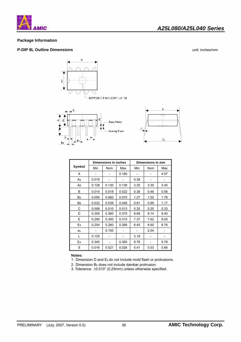
Package Information P-DIP 8L Outline Dimensions unit: inches/mm
Dimensions in inches Dimensions in mm Symbol Min Nom Max Min Nom Max
A - - 0.180 - - 4.57
A1 0.015 - - 0.38 - -
A2 0.128 0.130 0.136 3.25 3.30 3.45
B 0.014 0.018 0.022 0.36 0.46 0.56
B1 0.050 0.060 0.070 1.27 1.52 1.78
B2 0.032 0.039 0.046 0.81 0.99 1.17
C 0.008 0.010 0.013 0.20 0.25 0.33D 0.350 0.360 0.370 8.89 9.14 9.40
E 0.290 0.300 0.315 7.37 7.62 8.00
E1 0.254 0.260 0.266 6.45 6.60 6.76
e1 - 0.100 - - 2.54 -
L 0.125 - - 3.18 - -
EA 0.345 - 0.385 8.76 - 9.78
S 0.016 0.021 0.026 0.41 0.53 0.66
Notes: 1. Dimension D and E1 do not include mold flash or protrusions. 2. Dimension B1 does not include dambar protrusion. 3. Tolerance: ±0.010” (0.25mm) unless otherwise specified.
A25L080/A25L040 Series
PRELIMINARY (July, 2007, Version 0.0) 39 AMIC Technology Corp.
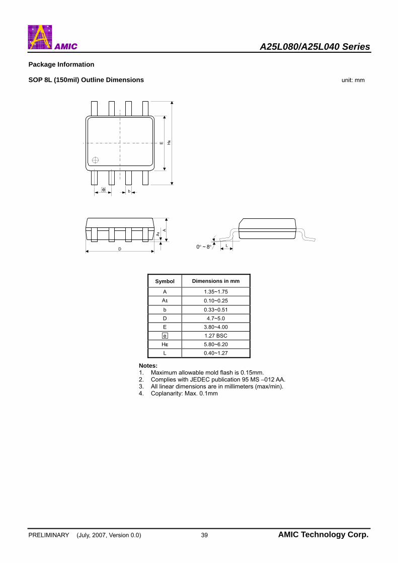
Package Information SOP 8L (150mil) Outline Dimensions unit: mm
HE
D
AA1
E
b
L°° 8~0
e
Symbol Dimensions in mm
A 1.35~1.75 A1 0.10~0.25
b 0.33~0.51 D 4.7~5.0 E 3.80~4.00 e 1.27 BSC
HE 5.80~6.20 L 0.40~1.27
Notes: 1. Maximum allowable mold flash is 0.15mm. 2. Complies with JEDEC publication 95 MS –012 AA. 3. All linear dimensions are in millimeters (max/min). 4. Coplanarity: Max. 0.1mm

A25L080/A25L040 Series
PRELIMINARY (July, 2007, Version 0.0) 40 AMIC Technology Corp.
Package Information SOP 8L (209mil) Outline Dimensions unit: mm
E
41
e b
8 5
D
A2 AA1
Lθ
E1
0.25
GAGE PLANESEATING PLANE
C
Dimensions in mm Symbol Min Nom Max
A 1.75 1.95 2.16
A1 0.05 0.15 0.25
A2 1.70 1.80 1.91 b 0.35 0.42 0.48 C 0.19 0.20 0.25 D 5.13 5.23 5.33
E 7.70 7.90 8.10 E1 5.18 5.28 5.38 e 1.27 BSC L 0.50 0.65 0.80
θ 0° - 8°
Notes: Maximum allowable mold flash is 0.15mm at the package ends and 0.25mm between leads


![Grammar Part 4 - Templeton Honors Collegetempletonhonorscollege.com/.../2014/...Part-4-by-Dr.-Fred-Putnam.pdf · The 3ms qal perfect (]exica] form) of many stative verbs is identica]](https://static.fdocuments.in/doc/165x107/5a8ddf307f8b9abb068cca83/grammar-part-4-templeton-honors-collegete-3ms-qal-perfect-exica-form-of-many.jpg)

