to lighting circuit to include a stepdown transformer (not ...
Upload
trannguyetCategory
view
215download
0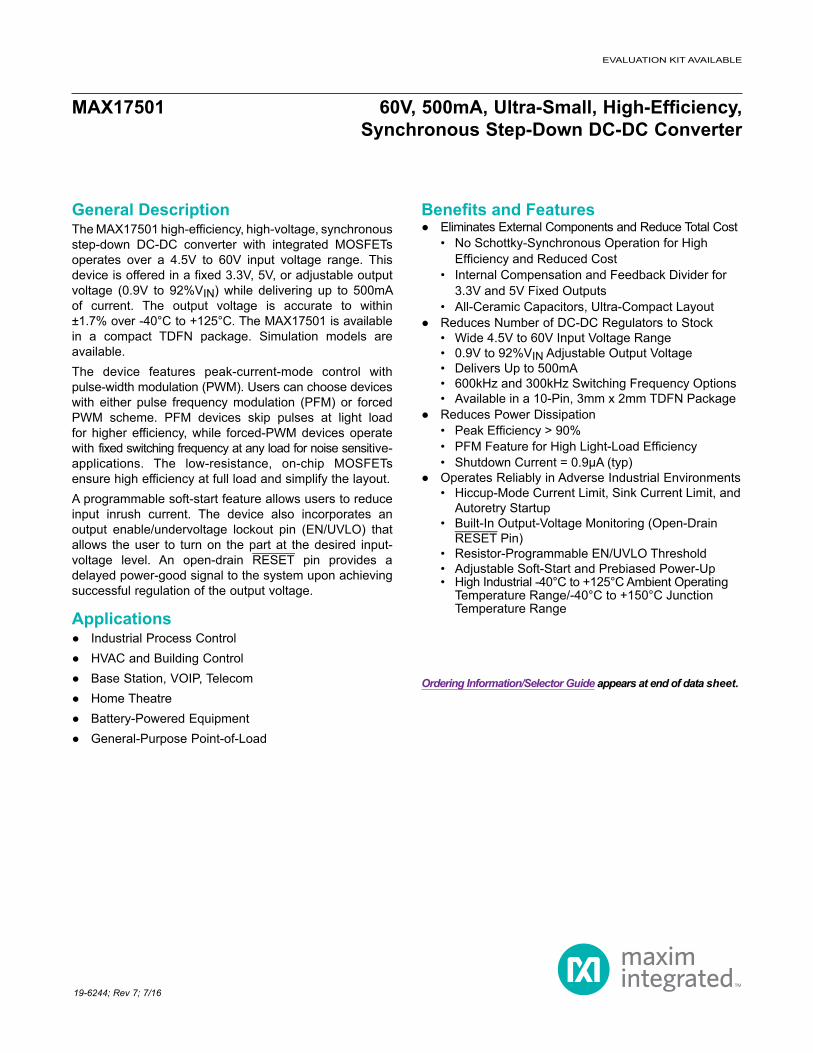
MAX17501 60V, 500mA, Ultra-Small, High-Efficiency, Synchronous Step-Down DC-DC Converter
General DescriptionThe MAX17501 high-efficiency, high-voltage, synchro nous step-down DC-DC converter with integrated MOSFETs operates over a 4.5V to 60V input voltage range. This device is offered in a fixed 3.3V, 5V, or adjustable output voltage (0.9V to 92%VIN) while delivering up to 500mA of current. The output voltage is accurate to within ±1.7% over -40°C to +125°C. The MAX17501 is available in a compact TDFN package. Simulation models are available.The device features peak-current-mode control with pulse-width modulation (PWM). Users can choose devices with either pulse frequency modulation (PFM) or forced PWM scheme. PFM devices skip pulses at light load for higher efficiency, while forced-PWM devices operate with fixed switching frequency at any load for noise sensitive- applications. The low-resistance, on-chip MOSFETs ensure high efficiency at full load and simplify the layout.A programmable soft-start feature allows users to reduce input inrush current. The device also incorporates an output enable/undervoltage lockout pin (EN/UVLO) that allows the user to turn on the part at the desired input-voltage level. An open-drain RESET pin provides a delayed power-good signal to the system upon achieving successful regulation of the output voltage.
Applications Industrial Process Control HVAC and Building Control Base Station, VOIP, Telecom Home Theatre Battery-Powered Equipment General-Purpose Point-of-Load
Benefits and Features Eliminates External Components and Reduce Total Cost• No Schottky-Synchronous Operation for High EfficiencyandReducedCost
• Internal Compensation and Feedback Divider for 3.3V and 5V Fixed Outputs
• All-Ceramic Capacitors, Ultra-Compact Layout Reduces Number of DC-DC Regulators to Stock• Wide 4.5V to 60V Input Voltage Range• 0.9V to 92%VIN Adjustable Output Voltage• Delivers Up to 500mA• 600kHz and 300kHz Switching Frequency Options• Available in a 10-Pin, 3mm x 2mm TDFN Package
Reduces Power Dissipation• PeakEfficiency>90%• PFMFeatureforHighLight-LoadEfficiency• ShutdownCurrent=0.9μA(typ)
Operates Reliably in Adverse Industrial Environments • Hiccup-Mode Current Limit, Sink Current Limit, and
Autoretry Startup• Built-In Output-Voltage Monitoring (Open-Drain RESET Pin)
• Resistor-Programmable EN/UVLO Threshold• Adjustable Soft-Start and Prebiased Power-Up• High Industrial -40°C to +125°C Ambient Operating
Temperature Range/-40°C to +150°C Junction Temperature Range
19-6244; Rev 7; 7/16
Ordering Information/Selector Guide appears at end of data sheet.
EVALUATION KIT AVAILABLE
MAX17501 60V, 500mA, Ultra-Small, High-Efficiency, Synchronous Step-Down DC-DC Converter
www.maximintegrated.com Maxim Integrated 2
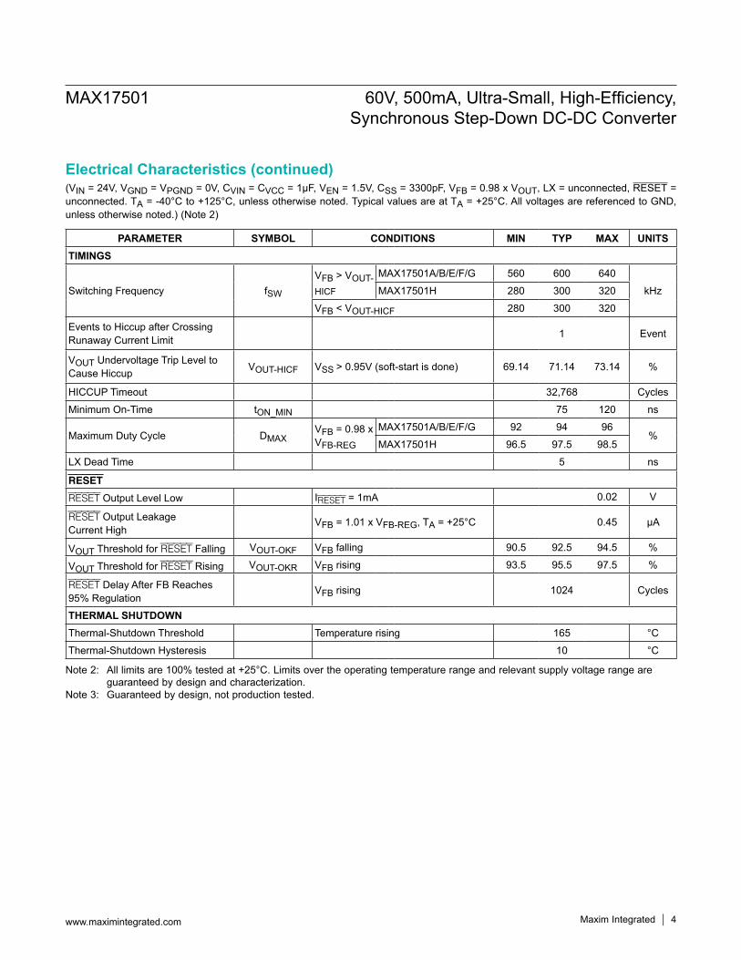
Electrical Characteristics(VIN = 24V, VGND = VPGND = 0V, CVIN = CVCC=1μF,VEN = 1.5V, CSS = 3300pF, VFB = 0.98 x VOUT, LX = unconnected, RESET = unconnected. TA = -40°C to +125°C, unless otherwise noted. Typical values are at TA = +25°C. All voltages are referenced to GND, unless otherwise noted.) (Note 2)
Note 1: Package thermal resistances were obtained using the method described in JEDEC specification JESD51-7, using a four-layer board. For detailed information on package thermal considerations, refer to www.maximintegrated.com/thermal-tutorial.
VIN to GND.............................................................-0.3V to +70V EN/UVLO to GND.......................................-0.3V to (VIN + 0.3V) LX to PGND................................................-0.3V to (VIN + 0.3V)FB, RESET, COMP, SS to GND .............................-0.3V to +6V VCC to GND..............................................................-0.3V to +6V GND to PGND.......................................................-0.3V to +0.3V LX Total RMS Current......................................................... ±1.6A Output Short-Circuit Duration.....................................Continuous
Continuous Power Dissipation (TA = +70°C) (derate 14.9mW/°C above +70°C) (multilayer board) .1188.7mWJunction Temperature......................................................+150°C Storage Temperature Range............................. -65°C to +160°C Lead Temperature (soldering, 10s).................................+300°C Soldering Temperature (reflow).......................................+260°C
Stresses beyond those listed under “Absolute Maximum Ratings” may cause permanent damage to the device. These are stress ratings only, and functional operation of the device at these or any other conditions beyond those indicated in the operational sections of the specifications is not implied. Exposure to absolute maximum rating conditions for extended periods may affect device reliability. Junction temperature greater than +125°C degrades operating lifetimes.
Package Thermal Characteristics (Note 1)TDFN Junction-to-AmbientThermalResistance(θJA) .......67.3°C/W Junction-to-CaseThermalResistance(θJC) ............18.2°C/W
Absolute Maximum Ratings
PARAMETER SYMBOL CONDITIONS MIN TYP MAX UNITSINPUT SUPPLY (VIN)Input Voltage Range VIN 4.5 60 V
Input Supply Current
IIN-SH VEN = 0V, shutdown mode 0.9 3.5µA
IIN-HIBERNATE VFB = 1.03 x VOUT, MAX17501A/B 90 145
IIN-SWNormal switching mode, no load
MAX17501E/F/G 4.75 6.75mA
MAX17501H 2.5 3.6
ENABLE/UVLO (EN/UVLO)
EN Threshold
VENR VEN rising 1.194 1.218 1.236
VVENF VEN falling 1.114 1.135 1.156
VEN-TRUESD VEN falling, true shutdown 0.7
EN Input Leakage Current IEN VEN = VIN = 60V, TA = +25°C 8 200 nA
LDO
VCC Output Voltage Range VCC6V < VIN < 12V, 0mA < IVCC < 10mA, 12V < VIN < 60V, 0mA < IVCC < 2mA 4.65 5 5.35 V
VCC Current Limit IVCC-MAX VCC = 4.3V, VIN = 12V 15 40 80 mA
VCC Dropout VCC-DO VIN = 4.5V, IVCC = 5mA 4.1 V
VCC UVLOVCC-UVR VCC rising 3.85 4 4.15
VVCC-UVF VCC falling 3.55 3.7 3.85
MAX17501 60V, 500mA, Ultra-Small, High-Efficiency, Synchronous Step-Down DC-DC Converter
www.maximintegrated.com Maxim Integrated 3
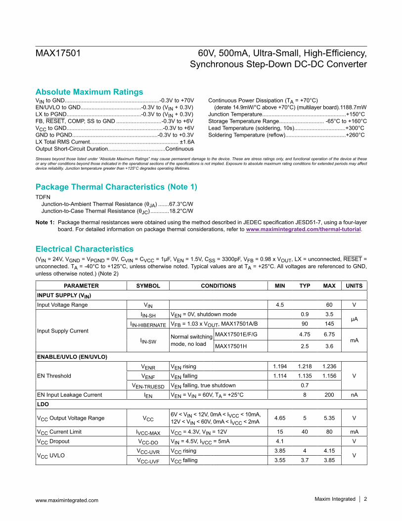
Electrical Characteristics (continued)(VIN = 24V, VGND = VPGND = 0V, CVIN = CVCC=1μF,VEN = 1.5V, CSS = 3300pF, VFB = 0.98 x VOUT, LX = unconnected, RESET = unconnected. TA = -40°C to +125°C, unless otherwise noted. Typical values are at TA = +25°C. All voltages are referenced to GND, unless otherwise noted.) (Note 2)
PARAMETER SYMBOL CONDITIONS MIN TYP MAX UNITSPOWER MOSFETs
High-Side pMOS On-Resistance RDS-ONHILX = 0.5A (sourcing)
TA = +25°C 0.55 0.85ΩTA = TJ = +125°C
(Note 3) 1.2
Low-Side nMOS On-Resistance RDS-ONLILX = 0.5A (sinking)
TA = +25°C 0.2 0.35ΩTA = TJ = +125°C
(Note 3) 0.47
LX Leakage Current ILX_LKGVEN = 0V, TA = +25°C, VLX = (VPGND + 1V) to (VIN - 1V) 1 µA
SOFT-START (SS)Charging Current ISS VSS = 0.5V 4.7 5 5.3 µA
FEEDBACK (FB/VO)FB Regulation Voltage VFB_REG MAX17501G/H 0.884 0.9 0.916 V
FB Input Bias Current IFB TA = +25NC
MAX17501A/E, VFB = 3.3V 6.8 12 17
µAMAX17501B/F, VFB = 5V 6.8 12 17
MAX17501G/H, VFB = 0.9V 100 nA
OUTPUT VOLTAGE (VOUT)
Output Voltage Accuracy VOUT
MAX17501A 3.248 3.380 3.448
VMAX17501B 4.922 5.121 5.225MAX17501E 3.248 3.3 3.352MAX17501F 4.922 5 5.08
TRANSCONDUCTANCE AMPLIFIER (COMP)Transconductance GM ICOMP = ±2.5µA, MAX17501G/H 510 590 650 µS
COMP Source Current ICOMP_SRC MAX17501G/H 19 32 55 µA
COMP Sink Current ICOMP_SINK MAX17501G/H 19 32 55 µA
Current-Sense Transresistance RCS MAX17501G/H 0.9 1 1.1 V/A
CURRENT LIMITPeak Current-Limit Threshold IPEAK-LIMIT 0.64 0.76 0.86 A
Runaway Current-Limit Threshold IRUNAWAY-LIMIT
0.65 0.78 0.905 A
Sink Current-Limit Threshold ISINK-LIMITMAX17501A/B 0.03
AMAX17501E/F/G/H 0.3 0.35 0.4
PFM Current-Limit Threshold IPFM MAX17501A/B 0.125 A
MAX17501 60V, 500mA, Ultra-Small, High-Efficiency, Synchronous Step-Down DC-DC Converter
www.maximintegrated.com Maxim Integrated 4
Electrical Characteristics (continued)(VIN = 24V, VGND = VPGND = 0V, CVIN = CVCC=1μF,VEN = 1.5V, CSS = 3300pF, VFB = 0.98 x VOUT, LX = unconnected, RESET = unconnected. TA = -40°C to +125°C, unless otherwise noted. Typical values are at TA = +25°C. All voltages are referenced to GND, unless otherwise noted.) (Note 2)
Note 2: All limits are 100% tested at +25°C. Limits over the operating temperature range and relevant supply voltage range are guaranteed by design and characterization.
Note 3: Guaranteed by design, not production tested.
PARAMETER SYMBOL CONDITIONS MIN TYP MAX UNITSTIMINGS
Switching Frequency fSW
VFB>VOUT-HICF
MAX17501A/B/E/F/G 560 600 640
kHzMAX17501H 280 300 320
VFB < VOUT-HICF 280 300 320
Events to Hiccup after Crossing Runaway Current Limit 1 Event
VOUT Undervoltage Trip Level to Cause Hiccup VOUT-HICF VSS >0.95V(soft-startisdone) 69.14 71.14 73.14 %
HICCUP Timeout 32,768 Cycles
Minimum On-Time tON_MIN 75 120 ns
Maximum Duty Cycle DMAXVFB = 0.98 x VFB-REG
MAX17501A/B/E/F/G 92 94 96%
MAX17501H 96.5 97.5 98.5
LX Dead Time 5 ns
RESET
RESET Output Level Low IRESET = 1mA 0.02 V
RESET Output Leakage Current High
VFB = 1.01 x VFB-REG, TA = +25°C 0.45 µA
VOUT Threshold for RESET Falling VOUT-OKF VFB falling 90.5 92.5 94.5 %
VOUT Threshold for RESET Rising VOUT-OKR VFB rising 93.5 95.5 97.5 %
RESET Delay After FB Reaches 95% Regulation
VFB rising 1024 Cycles
THERMAL SHUTDOWNThermal-Shutdown Threshold Temperature rising 165 °C
Thermal-Shutdown Hysteresis 10 °C
Maxim Integrated 5www.maximintegrated.com
MAX17501 60V, 500mA, Ultra-Small, High-Efficiency, Synchronous Step-Down DC-DC Converter
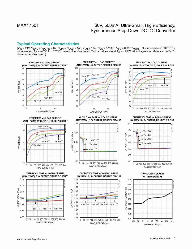
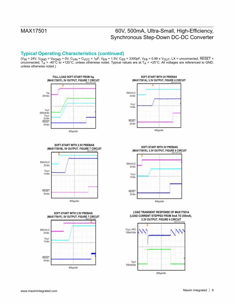
Typical Operating Characteristics(VIN = 24V, VGND = VPGND = 0V, CVIN = CVCC=1μF,VEN = 1.5V, CSS = 3300pF, VFB = 0.98 x VOUT, LX = unconnected, RESET = unconnected, TA = -40°C to +125°C, unless otherwise noted. Typical values are at TA = +25°C. All voltages are referenced to GND, unless otherwise noted.)
EFFICIENCY vs. LOAD CURRENT(MAX17501A), 3.3V OUTPUT, FIGURE 6 CIRCUIT
LOAD CURRENT (mA)
EFFI
CIEN
CY (%
)
10010
40
50
60
70
80
90
100
301
VIN = 12VVIN = 24V
VIN = 36V
MAX
1750
1 to
c01
EFFICIENCY vs. LOAD CURRENT(MAX17501B), 5V OUTPUT, FIGURE 7 CIRCUIT
LOAD CURRENT (mA)
EFFI
CIEN
CY (%
)
10010
40
50
60
70
80
90
100
301
VIN = 12VVIN = 24V
VIN = 36V VIN = 48V
MAX
1750
1 to
c02
EFFICIENCY vs. LOAD CURRENT(MAX17501E), 3.3V OUTPUT, FIGURE 6 CIRCUIT
LOAD CURRENT (mA)
EFFI
CIEN
CY (%
)
450400300 350150 200 250100
50
55
60
65
70
75
80
85
90
95
4550 500
VIN = 36VVIN = 24V
VIN = 12V
MAX
1750
1 to
c03
EFFICIENCY vs. LOAD CURRENT(MAX17501F), 5V OUTPUT, FIGURE 7 CIRCUIT
LOAD CURRENT (mA)
EFFI
CIEN
CY (%
)
450400300 350150 200 250100
50
60
70
80
90
100
4050 500
VIN = 48V
VIN = 12V
VIN = 36V
VIN = 24V
MAX
1750
1 to
c04
OUTPUT VOLTAGE vs. LOAD CURRENT(MAX17501A), 3.3V OUTPUT, FIGURE 6 CIRCUIT
LOAD CURRENT (mA)
OUTP
UT V
OLTA
GE (V
)
45040035030025020015010050
3.30
3.35
3.40
3.45
3.250 500
VIN = 36V
VIN = 24V
VIN = 12V
MAX
1750
1 to
c05
OUTPUT VOLTAGE vs. LOAD CURRENT(MAX17501B), 5V OUTPUT, FIGURE 7 CIRCUIT
LOAD CURRENT (mA)
OUTP
UT V
OLTA
GE (V
)
45040035030025020015010050
4.95
5.15
5.10
5.05
5.00
5.20
4.900 500
VIN = 12V
VIN = 24V
VIN = 36V
VIN = 48V
MAX
1750
1 to
c06
OUTPUT VOLTAGE vs. LOAD CURRENT(MAX17501E), 3.3V OUTPUT, FIGURE 6 CIRCUIT
LOAD CURRENT (mA)
OUTP
UT V
OLTA
GE (V
)
450400350300250200150100500 500
3.295
3.300
3.305
3.310
3.315
3.320
3.290
VIN = 24VVIN = 12V VIN = 36V
MAX
1750
1 to
c07
OUTPUT VOLTAGE vs. LOAD CURRENT(MAX17501F), 5V OUTPUT, FIGURE 7 CIRCUIT
LOAD CURRENT (mA)
OUTP
UT V
OLTA
GE (V
)
450400350300250200150100500 500
4.97
4.96
4.98
4.99
5.00
5.01
5.03
5.02
5.04
5.05
4.95
VIN = 48V VIN = 36V VIN = 24V VIN = 12V
MAX
1750
1 to
c08
SHUTDOWN CURRENTvs. TEMPERATURE
MAX
1750
1 to
c09
TEMPERATURE (°C)
SHUT
DOW
N CU
RREN
T (µ
A)
100 120806040200-20
0.75
0.80
0.85
0.90
0.95
1.00
1.05
1.10
0.70-40
Maxim Integrated 6www.maximintegrated.com
MAX17501 60V, 500mA, Ultra-Small, High-Efficiency, Synchronous Step-Down DC-DC Converter
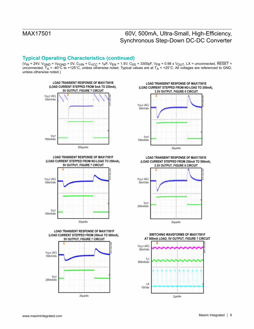
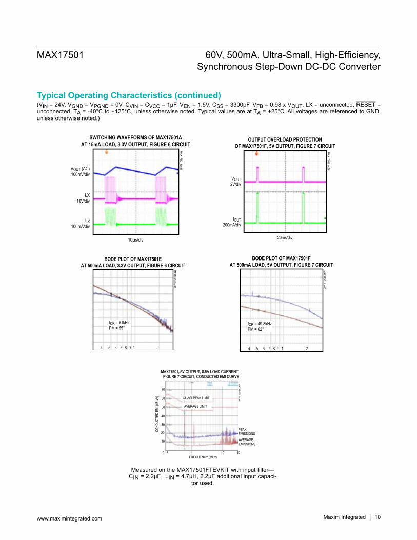
Typical Operating Characteristics (continued)(VIN = 24V, VGND = VPGND = 0V, CVIN = CVCC=1μF,VEN = 1.5V, CSS = 3300pF, VFB = 0.98 x VOUT, LX = unconnected, RESET = unconnected, TA = -40°C to +125°C, unless otherwise noted. Typical values are at TA = +25°C. All voltages are referenced to GND, unless otherwise noted.)
NO-LOAD SWITCHING CURRENTvs. TEMPERATURE (PFM OPERATION)
MAX
1750
1 to
c10
TEMPERATURE (°C)
NO-L
OAD
SWIT
CHIN
G CU
RREN
T (µ
A)
100 120806040200-20
60
80
100
120
140
40-40
NO-LOAD SWITCHING CURRENT vs. TEMPERATURE(FORCED-PWM OPERATION)
MAX
1750
1 to
c11
TEMPERATURE (°C)
NO-L
OAD
SWIT
CHIN
G CU
RREN
T (m
A)
100 120806040200-20
4.85
4.90
4.95
5.00
4.80-40
EN/UVLO THRESHOLDvs. TEMPERATURE
MAX
1750
1 to
c12
TEMPERATURE (°C)
EN/U
VLO
THRE
SHOL
D VO
LTAG
E (V
)
100 120806040200-20
1.131.14
1.16
1.18
1.20
1.231.221.21
1.19
1.17
1.15
1.12-40
RISINGTHRESHOLD
FALLINGTHRESHOLD
NO-LOAD OUTPUT VOLTAGEvs. TEMPERATURE (MAX17501E), 3.3V OUTPUT, FIGURE 6 CIRCUIT
MAX
1750
1 to
c13
TEMPERATURE (°C)
OUTP
UT V
OLTA
GE (V
)
100 120806040200-20
3.275
3.300
3.325
3.350
3.250-40
NO-LOAD OUTPUT VOLTAGEvs. TEMPERATURE (MAX17501F),
5V OUTPUT, FIGURE 7 CIRCUITM
AX17
501
toc1
4
TEMPERATURE (°C)
OUTP
UT V
OLTA
GE (V
)
100 120806040200-20
4.975
5.000
5.025
5.050
4.950-40
FEEDBACK VOLTAGEvs. TEMPERATURE
MAX
1750
1 to
c15
TEMPERATURE (°C)
FEED
BACK
VOL
TAGE
(V)
100 120806040200-20
0.89
0.90
0.91
0.92
0.88-40
PEAK AND RUNAWAY CURRENT LIMITvs. TEMPERATURE
MAX
1750
1 to
c16
TEMPERATURE (°C)
CURR
ENT
LIMIT
(A)
100 120806040200-20
0.75
0.70
0.65
0.80
0.85
0.90
0.60-40
PEAKCURRENT
LIMIT
RUNAWAYCURRENT
LIMIT
SWITCHING FREQUENCYvs. TEMPERATURE
MAX
1750
1 to
c17
TEMPERATURE (°C)
SWIT
CHIN
G FR
EQUE
NCY
(kHz)
100 120806040200-20
400
300
500
600
700
200-40
NO-LOAD SOFT-START FROM EN/UVLO(MAX17501A), 3.3V OUTPUT, FIGURE 6 CIRCUIT
MAX17501 toc18
1ms/div
EN/UVLO2V/div
VOUT1V/div
RESET2V/div
Maxim Integrated 7www.maximintegrated.com
MAX17501 60V, 500mA, Ultra-Small, High-Efficiency, Synchronous Step-Down DC-DC Converter
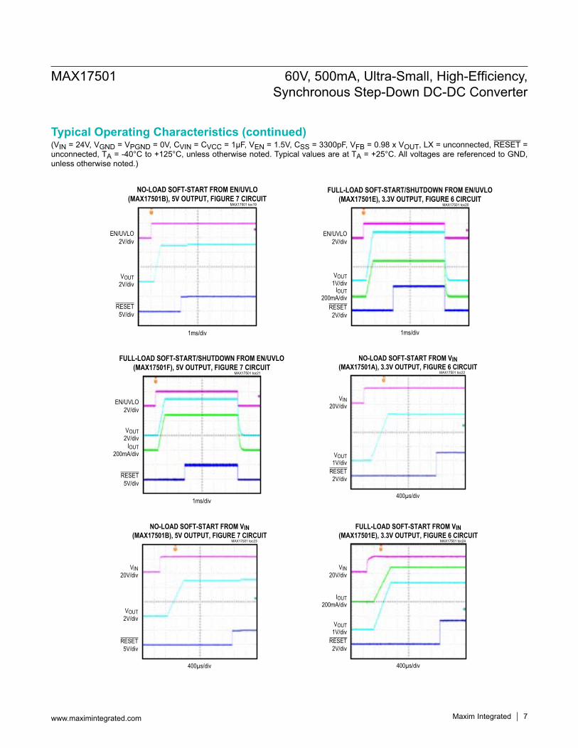
Typical Operating Characteristics (continued)(VIN = 24V, VGND = VPGND = 0V, CVIN = CVCC=1μF,VEN = 1.5V, CSS = 3300pF, VFB = 0.98 x VOUT, LX = unconnected, RESET = unconnected, TA = -40°C to +125°C, unless otherwise noted. Typical values are at TA = +25°C. All voltages are referenced to GND, unless otherwise noted.)
NO-LOAD SOFT-START FROM EN/UVLO(MAX17501B), 5V OUTPUT, FIGURE 7 CIRCUIT
MAX17501 toc19
1ms/div
EN/UVLO2V/div
VOUT2V/div
RESET5V/div
FULL-LOAD SOFT-START/SHUTDOWN FROM EN/UVLO(MAX17501E), 3.3V OUTPUT, FIGURE 6 CIRCUIT
MAX17501 toc20
1ms/div
EN/UVLO2V/div
VOUT1V/div
IOUT200mA/div
RESET2V/div
FULL-LOAD SOFT-START/SHUTDOWN FROM EN/UVLO(MAX17501F), 5V OUTPUT, FIGURE 7 CIRCUIT
MAX17501 toc21
1ms/div
EN/UVLO2V/div
VOUT2V/div
IOUT200mA/div
RESET5V/div
NO-LOAD SOFT-START FROM VIN(MAX17501A), 3.3V OUTPUT, FIGURE 6 CIRCUIT
MAX17501 toc22
400µs/div
VIN20V/div
VOUT1V/div
RESET2V/div
NO-LOAD SOFT-START FROM VIN(MAX17501B), 5V OUTPUT, FIGURE 7 CIRCUIT
MAX17501 toc23
400µs/div
VIN20V/div
VOUT2V/div
RESET5V/div
FULL-LOAD SOFT-START FROM VIN(MAX17501E), 3.3V OUTPUT, FIGURE 6 CIRCUIT
MAX17501 toc24
400µs/div
VIN20V/div
VOUT1V/div
IOUT200mA/div
RESET2V/div
Maxim Integrated 8www.maximintegrated.com
MAX17501 60V, 500mA, Ultra-Small, High-Efficiency, Synchronous Step-Down DC-DC Converter
Typical Operating Characteristics (continued)(VIN = 24V, VGND = VPGND = 0V, CVIN = CVCC=1μF,VEN = 1.5V, CSS = 3300pF, VFB = 0.98 x VOUT, LX = unconnected, RESET = unconnected, TA = -40°C to +125°C, unless otherwise noted. Typical values are at TA = +25°C. All voltages are referenced to GND, unless otherwise noted.)
FULL-LOAD SOFT-START FROM VIN(MAX17501F), 5V OUTPUT, FIGURE 7 CIRCUIT
MAX17501 toc25
400µs/div
VIN20V/div
VOUT2V/div
IOUT200mA/div
RESET5V/div
SOFT-START WITH 2V PREBIAS(MAX17501A), 3.3V OUTPUT, FIGURE 6 CIRCUIT
MAX17501 toc26
400µs/div
EN/UVLO2V/div
VOUT1V/div
RESET2V/div
SOFT-START WITH 2.5V PREBIAS(MAX17501B), 5V OUTPUT, FIGURE 7 CIRCUIT
MAX17501 toc27
400µs/div
EN/UVLO2V/div
VOUT1V/div
RESET5V/div
SOFT-START WITH 2V PREBIAS(MAX17501E), 3.3V OUTPUT, FIGURE 6 CIRCUIT
MAX17501 toc28
400µs/div
EN/UVLO2V/div
VOUT1V/div
RESET2V/div
SOFT-START WITH 2.5V PREBIAS(MAX17501F), 5V OUTPUT, FIGURE 7 CIRCUIT
MAX17501 toc29
400µs/div
EN/UVLO2V/div
VOUT1V/div
RESET5V/div
LOAD TRANSIENT RESPONSE OF MAX17501A(LOAD CURRENT STEPPED FROM 5mA TO 255mA),
3.3V OUTPUT, FIGURE 6 CIRCUITMAX17501 toc30
200µs/div
VOUT (AC)100mV/div
IOUT100mA/div
Maxim Integrated 9www.maximintegrated.com
MAX17501 60V, 500mA, Ultra-Small, High-Efficiency, Synchronous Step-Down DC-DC Converter
Typical Operating Characteristics (continued)(VIN = 24V, VGND = VPGND = 0V, CVIN = CVCC=1μF,VEN = 1.5V, CSS = 3300pF, VFB = 0.98 x VOUT, LX = unconnected, RESET = unconnected, TA = -40°C to +125°C, unless otherwise noted. Typical values are at TA = +25°C. All voltages are referenced to GND, unless otherwise noted.)
LOAD TRANSIENT RESPONSE OF MAX17501B(LOAD CURRENT STEPPED FROM 5mA TO 255mA),
5V OUTPUT, FIGURE 7 CIRCUIT
MAX17501 toc31
200µs/div
VOUT (AC)100mV/div
IOUT100mA/div
LOAD TRANSIENT RESPONSE OF MAX17501E(LOAD CURRENT STEPPED FROM NO-LOAD TO 250mA),
3.3V OUTPUT, FIGURE 6 CIRCUIT
MAX17501 toc32
20µs/div
VOUT (AC)50mV/div
IOUT100mA/div
LOAD TRANSIENT RESPONSE OF MAX17501F(LOAD CURRENT STEPPED FROM NO-LOAD TO 250mA),
5V OUTPUT, FIGURE 7 CIRCUIT
MAX17501 toc33
20µs/div
VOUT (AC)100mV/div
IOUT100mA/div
LOAD TRANSIENT RESPONSE OF MAX17501F(LOAD CURRENT STEPPED FROM 250mA TO 500mA),
5V OUTPUT, FIGURE 7 CIRCUIT
MAX17501 toc35
20µs/div
VOUT (AC)100mV/div
IOUT200mA/div
LOAD TRANSIENT RESPONSE OF MAX17501E(LOAD CURRENT STEPPED FROM 250mA TO 500mA),
3.3V OUTPUT, FIGURE 6 CIRCUIT
MAX17501 toc34
20µs/div
VOUT (AC)50mV/div
IOUT200mA/div
SWITCHING WAVEFORMS OF MAX17501FAT 500mA LOAD, 5V OUTPUT, FIGURE 7 CIRCUIT
MAX17501 toc36
2µs/div
VOUT (AC)50mV/div
ILX500mA/div
LX10V/div
Maxim Integrated 10www.maximintegrated.com
MAX17501 60V, 500mA, Ultra-Small, High-Efficiency, Synchronous Step-Down DC-DC Converter
Typical Operating Characteristics (continued)(VIN = 24V, VGND = VPGND = 0V, CVIN = CVCC=1μF,VEN = 1.5V, CSS = 3300pF, VFB = 0.98 x VOUT, LX = unconnected, RESET = unconnected, TA = -40°C to +125°C, unless otherwise noted. Typical values are at TA = +25°C. All voltages are referenced to GND, unless otherwise noted.)
SWITCHING WAVEFORMS OF MAX17501AAT 15mA LOAD, 3.3V OUTPUT, FIGURE 6 CIRCUIT
MAX17501 toc37
10µs/div
VOUT (AC)100mV/div
ILX100mA/div
LX10V/div
OUTPUT OVERLOAD PROTECTIONOF MAX17501F, 5V OUTPUT, FIGURE 7 CIRCUIT
MAX17501 toc38
20ms/div
VOUT2V/div
IOUT200mA/div
BODE PLOT OF MAX17501EAT 500mA LOAD, 3.3V OUTPUT, FIGURE 6 CIRCUIT
MAX17501 toc39
fCR = 51kHzPM = 55°
4 5 6 7 8 9 1 2
BODE PLOT OF MAX17501FAT 500mA LOAD, 5V OUTPUT, FIGURE 7 CIRCUIT
MAX17501 toc40
fCR = 49.8kHzPM = 62°
4 5 6 7 8 9 1 2
MA
X17501toc41
MAX17501, 5V OUTPUT, 0.5A LOAD CURRENT,FIGURE 7 CIRCUIT, CONDUCTED EMI CURVE
0.15 1 10 30
AVERAGEEMISSIONS
PEAKEMISSIONS
CO
ND
UC
TED
EMI(
dBµ
V)
FREQUENCY (MHz)
10
20
30
40
50
60
70
QUASI-PEAK LIMIT
AVERAGE LIMIT
Measured on the MAX17501FTEVKIT with input filter—CIN = 2.2µF, LIN = 4.7µH, 2.2µF additional input capaci-
tor used.
MAX17501 60V, 500mA, Ultra-Small, High-Efficiency, Synchronous Step-Down DC-DC Converter
www.maximintegrated.com Maxim Integrated 11
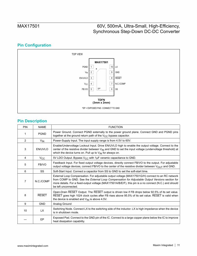
Pin Description
Pin Configuration
PIN NAME FUNCTION
1 PGND Power Ground. Connect PGND externally to the power ground plane. Connect GND and PGND pins together at the ground return path of the VCC bypass capacitor.
2 VIN Power-Supply Input. The input supply range is from 4.5V to 60V.
3 EN/UVLOEnable/Undervoltage Lockout Input. Drive EN/UVLO high to enable the output voltage. Connect to the center of the resistive divider between VIN and GND to set the input voltage (undervoltage threshold) at which the device turns on. Pull up to VIN for always on.
4 VCC 5V LDO Output. Bypass VCC with 1µF ceramic capacitance to GND.
5 FB/VO FeedbackInput.Forfixedoutputvoltagedevices,directlyconnectFB/VOtotheoutput.Foradjustableoutput voltage devices, connect FB/VO to the center of the resistive divider between VOUT and GND.
6 SS Soft-Start Input. Connect a capacitor from SS to GND to set the soft-start time.
7 N.C./COMP
External Loop Compensation. For adjustable output voltage (MAX17501G/H) connect to an RC network from COMP to GND. See the External Loop Compensation for Adjustable Output Versions section for moredetails.Forafixed-outputvoltage(MAX17501A/B/E/F),thispinisanoconnect(N.C.)andshouldbe left unconnected.
8 RESETOpen-Drain RESET Output. The RESET output is driven low if FB drops below 92.5% of its set value. RESET goes high 1024 clock cycles after FB rises above 95.5% of its set value. RESET is valid when the device is enabled and VIN is above 4.5V.
9 GND Analog Ground
10 LX Switching Node. Connect LX to the switching side of the inductor. LX is high impedance when the device is in shutdown mode.
— EP Exposed Pad. Connect to the GND pin of the IC. Connect to a large copper plane below the IC to improve heat dissipation capability.
TOP VIEW
*EP = EXPOSED PAD. CONNECT TO GND
TDFN(3mm x 2mm)
MAX175011
2
3
4
5
PGND
VIN
EN/UVLO
VCC
FB/VO
LX
GND
RESET
N.C./COMP
SS
+
EP*
10
9
8
7
6
MAX17501 60V, 500mA, Ultra-Small, High-Efficiency, Synchronous Step-Down DC-DC Converter
www.maximintegrated.com Maxim Integrated 12
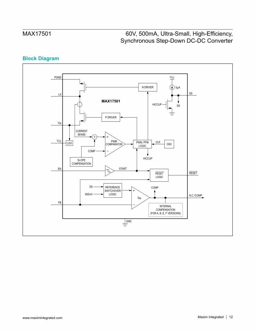
Block Diagram
PGND
LX
VIN
VCCLDO
SLOPECOMPENSATION
STARTRESETLOGIC
REFERENCESWITCHOVER
LOGIC
COMP
CURRENTSENSE
P DRIVER
PWM, PFMLOGIC
GM
GND
INTERNALCOMPENSATION
(FOR A, B, E, F VERSIONS)
N DRIVER
VCC
5µA
SS
RESET
N.C./COMP
SS
HICCUP
COMP
HICCUP
CLKOSC
PWMCOMPARATOR
EN
SS
900mV
FB
MAX17501
MAX17501 60V, 500mA, Ultra-Small, High-Efficiency, Synchronous Step-Down DC-DC Converter
www.maximintegrated.com Maxim Integrated 13
Detailed DescriptionThe MAX17501 synchronous step-down regulator oper-ates from 4.5V to 60V and delivers up to 500mA load current. Output voltage regulation accuracy meets ±1.7% over temperature.The device uses a peak-current-mode control scheme. An internal transconductance error amplifier generates an integrated error voltage. The error voltage sets the duty cycle using a PWM comparator, a high-side current-sense amplifier, and a slope-compensation generator. At each rising edge of the clock, the high-side p-channel MOSFET turns on and remains on until either the appropriate or maximum duty cycle is reached, or the peak current limit is detected.During the high-side MOSFET’s on-time, the inductor current ramps up. During the second half of the switching cycle, the high-side MOSFET turns off and the low-side n-channel MOSFET turns on and remains on until either the next rising edge of the clock arrives or sink current limit is detected. The inductor releases the stored energy as its current ramps down, and provides current to the output (the internal low RDSON pMOS/nMOS switches ensure high efficiency at full load).This device also integrates enable/undervoltage lockout (EN/UVLO), adjustable soft-start time (SS), and open-drain reset output (RESET) functionality.
PFM OperationThe A and B versions of the MAX17501 feature a PFM scheme to improve light load efficiency. At light loads, once the part enters PFM mode, the inductor current is forced to a fixed peak of 125mA (typical) every clock cycle until the output rises to 103.3% of nominal voltage. Once output reaches 103.3% of nominal voltage, both high-side and low-side FETs are turned off and the part enters hibernate operation until the load discharges output to 101.3% of nominal voltage. Most of the internal blocks are turned off in hibernate operation to save quiescent current. Such an operation reduces the effective switch-ing frequency of the converter at light loads, resulting in reduced switching losses and improved light load effi-ciency. The part naturally exits PFM mode when the load current exceeds 62.5mA (typical).
Linear Regulator (VCC)An internal linear regulator (VCC) provides a 5V nominal supply to power the internal blocks and the low-side MOSFET driver. The output of the VCC linear regulator should be bypassed with a 1μF ceramic capacitor toGND. The device employs an undervoltage-lockout circuit
that disables the internal linear regulator when VCC falls below 3.7V (typical). The internal VCC linear regulator can source up to 40mA (typical) to supply the device and to power the low-side gate driver.
Operating Input Voltage RangeThe maximum operating input voltage is determined by the minimum controllable on-time and the minimum oper-ating input voltage is determined by the maximum duty cycle and circuit voltage drops. The minimum and maxi-mum operating input voltages for a given output voltage should be calculated as:
OUT OUT(MAX) DCRIN(MIN)
MAX
OUT(MAX)
V (I (R 0.47))V
D(I 0.73)
+ × +=
+ ×
=×
OUTIN(MAX)
SW (MAX) ON(MIN)
VV
f t
where VOUT is the steady-state output voltage, IOUT(MAX) is the maximum load current, RDCR is the DC resistance of the inductor, fSW(MAX) is the switching frequency (max-imum) and tON(MIN) is the worst-case minimum switch on-time (120ns). The following table lists the fSW(MAX) and DMAX values to be used for calculation for different versions of the MAX17501:
Overcurrent Protection/HICCUP ModeThe device is provided with a robust overcurrent- protection scheme that protects the device under over-load and output short-circuit conditions. A cycle-by-cycle peak current limit turns off the high-side MOSFET when-ever the high-side switch current exceeds an internal limit of 760mA (typ). A runaway current limit on the high-side switch current at 780mA (typ) protects the device under high input voltage, short-circuit conditions when there is insufficient output voltage available to restore the inductor current that built up during the on period of the step-down converter. One occurrence of the runaway current limit triggers a hiccup mode. In addition, if due to a fault condition, output voltage drops to 71.14% (typ) of its nominal value any time after soft-start is complete, hiccup mode is triggered.In hiccup mode, the converter is protected by suspending switching for a hiccup timeout period of 32,768 clock
PART VERSION fSW (MAX) (kHz) DMAXMAX17501A/B/E/F/G 640 0.92
MAX17501H 320 0.965
MAX17501 60V, 500mA, Ultra-Small, High-Efficiency, Synchronous Step-Down DC-DC Converter
www.maximintegrated.com Maxim Integrated 14
cycles. Once the hiccup timeout period expires, soft-start is attempted again. This operation results in minimal power dissipation under overload fault conditions.
RESET OutputThe device includes a RESET comparator to monitor the output voltage. The open-drain RESET output requires an external pullup resistor. RESET can sink 2mA of current while low. RESET goes high (high impedance) 1024 switching cycles after the regulator output increases above 95.5% of the designated nominal regulated voltage. RESET goes low when the regulator output voltage drops to below 92.5% of the nominal regulated voltage. RESET also goes low during thermal shutdown. RESET is valid when the device is enabled and VIN is above 4.5V.
Prebiased OutputWhen the device starts into a prebiased output, both the high-side and low-side switches are turned off so the converter does not sink current from the output. High-side and low-side switches do not start switching until the PWM comparator commands the first PWM pulse, at which point switching commences first with the high-side switch. The output voltage is then smoothly ramped up to the target value in alignment with the internal reference.
Thermal-Overload ProtectionThermal-overload protection limits total power dissipa tion in the device. When the junction temperature of the device exceeds +165°C, an on-chip thermal sensor shuts down the device, allowing the device to cool. The thermal sensor turns the device on again after the junc tion temperature cools by 10°C. Soft-start resets during thermal shutdown. Carefully evaluate the total power dissipation (see the Power Dissipation section) to avoid unwanted triggering of the thermal-overload protection in normal operation.
Applications InformationInput Capacitor SelectionThe discontinuous input-current waveform of the buck converter causes large ripple currents in the input capaci-tor. The switching frequency, peak inductor cur rent, and the allowable peak-to-peak voltage ripple that reflects back to the source dictate the capacitance requirement. The device’s high switching frequency allows the use of smaller value input capacitors. X7R capacitors are rec-ommended in industrial applications for their temperature stability.Aminimumvalueof1μFshouldbeusedfortheinput capacitor. Higher values help reduce the ripple on the input DC bus further. In applications where the source
is located distant from the device input, an electrolytic capacitorshouldbeaddedinparalleltothe1μFceramiccapacitor to provide necessary damping for potential oscillations caused by the longer input power path and input ceramic capacitor.
Inductor SelectionThree key inductor parameters must be specified for operation with the device: inductance value (L), inductor saturation current (ISAT), and DC resistance (RDCR). The switching frequency and output voltage determine the inductor value as follows:
=LfSW
4.8 x VOUT
where VOUT and fSW are nominal values.Select a low-loss inductor closest to the calculated value with acceptable dimensions and having the lowest pos-sible DC resistance. The saturation current rating (ISAT) of the inductor must be high enough to ensure that satu-ration can occur only above the peak current-limit value (IPEAK-LIMIT (typ) = 0.76A for the device).
Output Capacitor SelectionX7R ceramic output capacitors are preferred due to their stability over temperature in industrial applications. The output capacitor is usually sized to support a step load of 50% of the maximum output current in the application, so the output-voltage deviation is contained to ±3% of the output-voltage change. For fixed 3.3V and 5V output voltage versions, connect aminimum of 10μF (1206) capacitor at the output. Foradjustable output voltage versions, the output capaci-tance can be calculated as follows:
×= ×
∆STEP RESPONSE
OUTOUT
I t1C2 V
≅ +RESPONSEC SW
0.33 1tf f
where ISTEP is the load current step, tRESPONSE is the response time of the controller, ΔVOUT is the allowable output-voltage deviation, fC is the target closed-loop cross-over frequency, and fSW is the switching frequency. Select fC to be 1/12th of fSW. Derating of ceramic capacitors with DC-voltage must be considered while selecting the output capacitor. Derating curves are available from all major ceramic capacitor vendors.
MAX17501 60V, 500mA, Ultra-Small, High-Efficiency, Synchronous Step-Down DC-DC Converter
www.maximintegrated.com Maxim Integrated 15
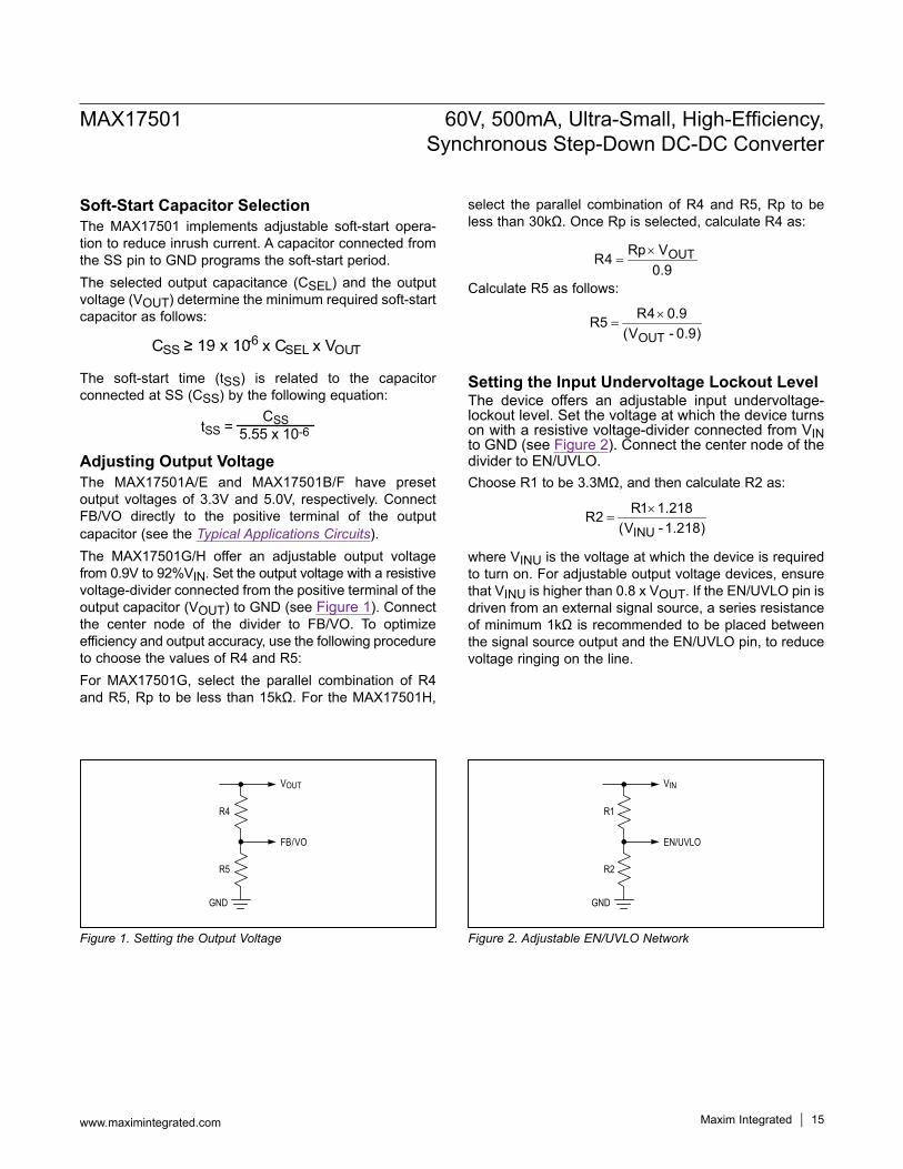
Figure 1. Setting the Output Voltage Figure 2. Adjustable EN/UVLO Network
Soft-Start Capacitor SelectionThe MAX17501 implements adjustable soft-start opera-tion to reduce inrush current. A capacitor con nected from the SS pin to GND programs the soft-start period.The selected output capacitance (CSEL) and the output voltage (VOUT) determine the minimum required soft-start capacitor as follows:
CSS-6 x CSEL x VOUT
The soft-start time (tSS) is related to the capacitor connected at SS (CSS) by the following equation:
tSS =CSS
5.55 x 10⁻⁶
Adjusting Output VoltageThe MAX17501A/E and MAX17501B/F have preset output voltages of 3.3V and 5.0V, respectively. Connect FB/VO directly to the positive terminal of the output capacitor (see the Typical Applications Circuits).The MAX17501G/H offer an adjustable output voltage from 0.9V to 92%VIN. Set the output voltage with a resistive voltage-divider connected from the positive terminal of the output capacitor (VOUT) to GND (see Figure 1). Connect the center node of the divider to FB/VO. To optimize efficiency and output accuracy, use the following procedure to choose the values of R4 and R5:For MAX17501G, select the parallel combination of R4 andR5,Rptobe lessthan15kΩ.For theMAX17501H,
select the parallel combination of R4 and R5, Rp to be lessthan30kΩ.OnceRpisselected,calculateR4as:
OUTRp VR40.9×
=
Calculate R5 as follows:
OUT
R4 0.9R5(V - 0.9)
×=
Setting the Input Undervoltage Lockout LevelThe device offers an adjustable input undervoltage-lockout level. Set the voltage at which the device turns on with a resistive voltage-divider connected from VIN to GND (see Figure 2). Connect the center node of the divider to EN/UVLO.ChooseR1tobe3.3MΩ,andthencalculateR2as:
INU
R1 1.218R2(V -1.218)
×=
where VINU is the voltage at which the device is required to turn on. For adjustable output voltage devices, ensure that VINU is higher than 0.8 x VOUT. If the EN/UVLO pin is driven from an external signal source, a series resistance ofminimum1kΩisrecommendedtobeplacedbetweenthe signal source output and the EN/UVLO pin, to reduce voltage ringing on the line.
R5
R4
FB/VO
GND
VOUT
R2
R1
EN/UVLO
GND
VIN
MAX17501 60V, 500mA, Ultra-Small, High-Efficiency, Synchronous Step-Down DC-DC Converter
www.maximintegrated.com Maxim Integrated 16
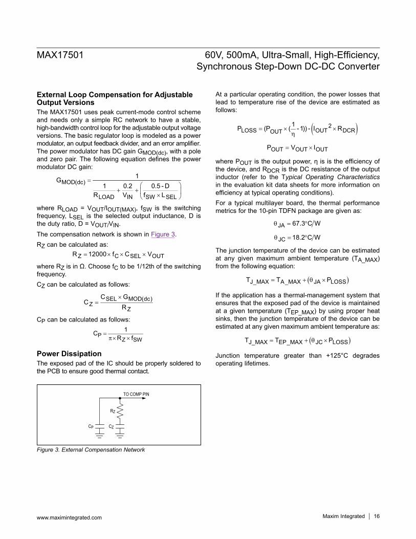
Figure 3. External Compensation Network
External Loop Compensation for Adjustable Output VersionsThe MAX17501 uses peak current-mode control scheme and needs only a simple RC network to have a stable, high-bandwidth control loop for the adjustable output voltage versions. The basic regulator loop is modeled as a power modulator, an output feedback divider, and an error amplifier. The power modulator has DC gain GMOD(dc), with a pole and zero pair. The following equation defines the power modulator DC gain:
=
+ + ×
MOD(dc)
LOAD IN SW SEL
1G1 0.2 0.5 - D
R V f L
where RLOAD = VOUT/IOUT(MAX), fSW is the switching frequency, LSEL is the selected output inductance, D is the duty ratio, D = VOUT/VIN. The compensation network is shown in Figure 3. RZ can be calculated as:
Z C SEL OUTR 12000 f C V= × × ×
where RZisinΩ.ChoosefC to be 1/12th of the switching frequency.CZ can be calculated as follows:
SEL MOD(dc)Z
Z
C GC
R×
=
CP can be calculated as follows:
=π× ×P
Z SW
1CR f
Power DissipationThe exposed pad of the IC should be properly soldered to the PCB to ensure good thermal contact.
At a particular operating condition, the power losses that lead to temperature rise of the device are estimated as follows:
( )2LOSS OUT DCROUT
1P (P ( -1)) - I R= × ×η
OUT OUT OUTP V I= ×
where POUT istheoutputpower,ηisistheefficiencyofthe device, and RDCR is the DC resistance of the output inductor (refer to the Typical Operating Characteristics in the evaluation kit data sheets for more information on efficiency at typical operating conditions).For a typical multilayer board, the thermal performance metrics for the 10-pin TDFN package are given as:
JA 67.3 C Wθ = °
JC 18.2 C Wθ = °
The junction temperature of the device can be estimated at any given maximum ambient temperature (TA_MAX) from the following equation:
( )J_MAX A_MAX JA LOSST T P= + θ ×
If the application has a thermal-management system that ensures that the exposed pad of the device is maintained at a given temperature (TEP_MAX) by using proper heat sinks, then the junction temperature of the device can be estimated at any given maximum ambient temperature as:
( )J_MAX EP_MAX JC LOSST T P= + θ ×
Junction temperature greater than +125°C degrades operating lifetimes.
RZ
TO COMP PIN
CZCP
MAX17501 60V, 500mA, Ultra-Small, High-Efficiency, Synchronous Step-Down DC-DC Converter
www.maximintegrated.com Maxim Integrated 17
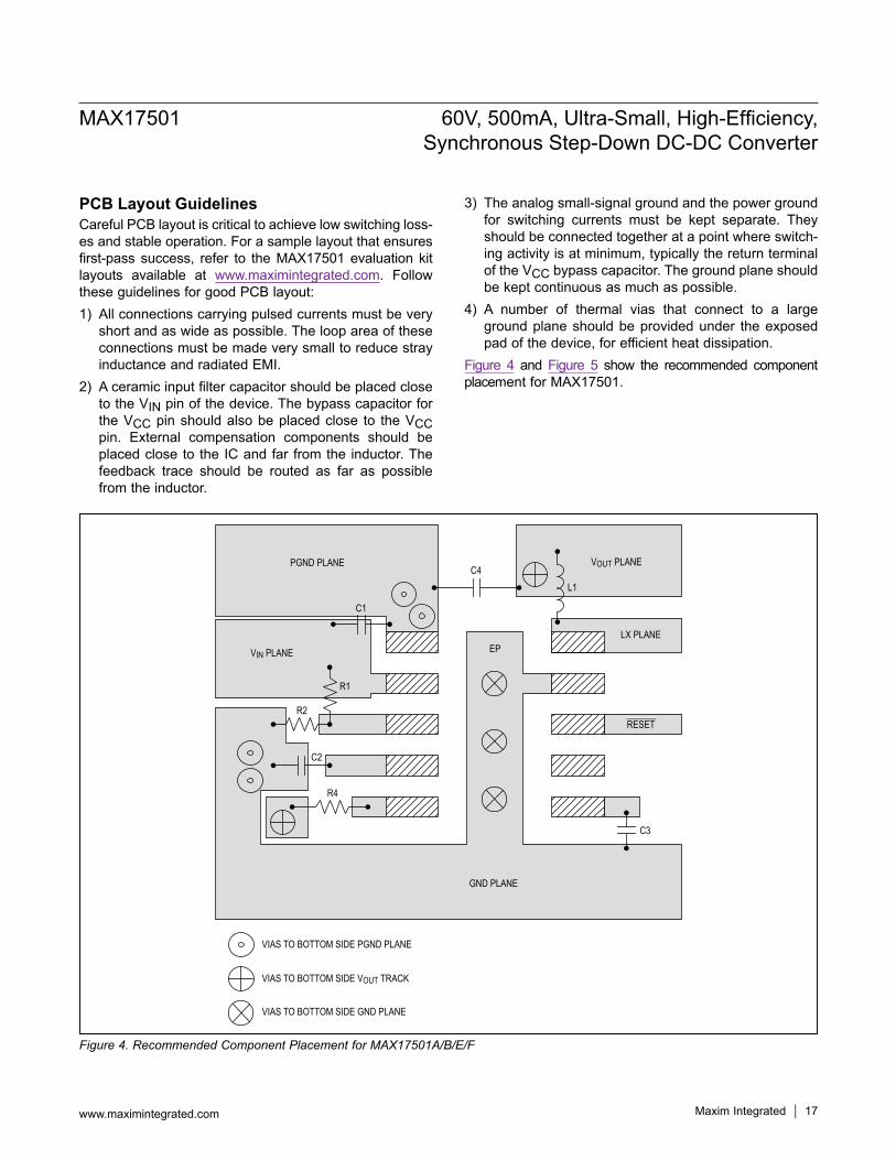
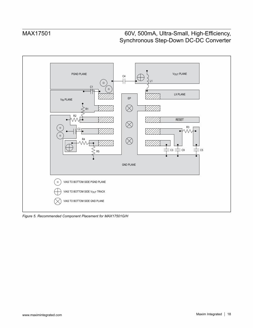
Figure 4. Recommended Component Placement for MAX17501A/B/E/F
PCB Layout GuidelinesCareful PCB layout is critical to achieve low switching loss-es and stable operation. For a sample layout that ensures first-pass success, refer to the MAX17501 evaluation kit layouts available at www.maximintegrated.com. Follow these guidelines for good PCB layout:1) All connections carrying pulsed currents must be very
short and as wide as possible. The loop area of these connections must be made very small to reduce stray inductance and radiated EMI.
2) A ceramic input filter capacitor should be placed close to the VIN pin of the device. The bypass capacitor for the VCC pin should also be placed close to the VCC pin. External compensation components should be placed close to the IC and far from the inductor. The feedback trace should be routed as far as possible from the inductor.
3) The analog small-signal ground and the power ground for switch ing currents must be kept separate. They should be connected together at a point where switch-ing activity is at minimum, typically the return terminal of the VCC bypass capacitor. The ground plane should be kept continuous as much as possible.
4) A number of thermal vias that connect to a large ground plane should be provided under the exposed pad of the device, for efficient heat dissipation.
Figure 4 and Figure 5 show the recommended component placement for MAX17501.
EP
R4
C2
C1
R2
R1
VIN PLANE
PGND PLANE
GND PLANE
VIAS TO BOTTOM SIDE PGND PLANE
VIAS TO BOTTOM SIDE VOUT TRACK
VIAS TO BOTTOM SIDE GND PLANE
L1
VOUT PLANE
LX PLANE
C3
RESET
C4
MAX17501 60V, 500mA, Ultra-Small, High-Efficiency, Synchronous Step-Down DC-DC Converter
www.maximintegrated.com Maxim Integrated 18
Figure 5. Recommended Component Placement for MAX17501G/H
EP
R4
R5
C2
C1
R2
R1
VIN PLANE
PGND PLANE
GND PLANE
L1
VOUT PLANE
LX PLANE
C3 C9 C5
R3
RESET
VIAS TO BOTTOM SIDE PGND PLANE
VIAS TO BOTTOM SIDE VOUT TRACK
VIAS TO BOTTOM SIDE GND PLANE
C4
MAX17501 60V, 500mA, Ultra-Small, High-Efficiency, Synchronous Step-Down DC-DC Converter
www.maximintegrated.com Maxim Integrated 19
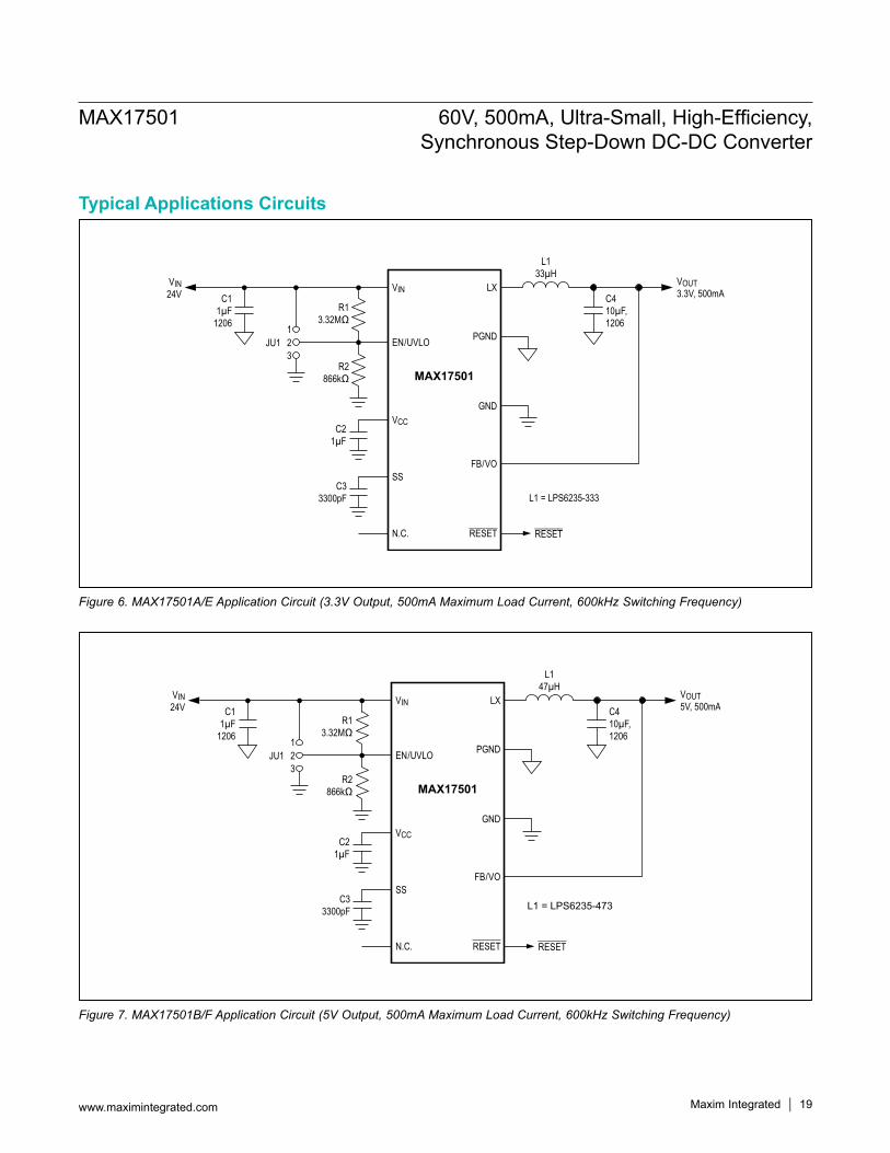
Typical Applications Circuits
Figure 6. MAX17501A/E Application Circuit (3.3V Output, 500mA Maximum Load Current, 600kHz Switching Frequency)
Figure 7. MAX17501B/F Application Circuit (5V Output, 500mA Maximum Load Current, 600kHz Switching Frequency)
C21µF
C33300pF
N.C.
SS
VCC
EN/UVLO
VIN LX
PGND
GND
FB/VO
L1 = LPS6235-333
RESET
VIN24V C1
1µF1206 1
2JU1
R13.32MΩ
R2866kΩ
3
MAX17501
RESET
L133µH
C410µF,1206
VOUT3.3V, 500mA
C21µF
C33300pF
N.C.
SS
VCC
EN/UVLO
VIN LX
PGND
GND
FB/VO
RESET
VIN24V C1
1µF1206 1
2JU1
R13.32MΩ
R2866kΩ
3
MAX17501
RESET
L147µH
C410µF,1206
VOUT5V, 500mA
L1 = LPS6235-473
MAX17501 60V, 500mA, Ultra-Small, High-Efficiency, Synchronous Step-Down DC-DC Converter
www.maximintegrated.com Maxim Integrated 20
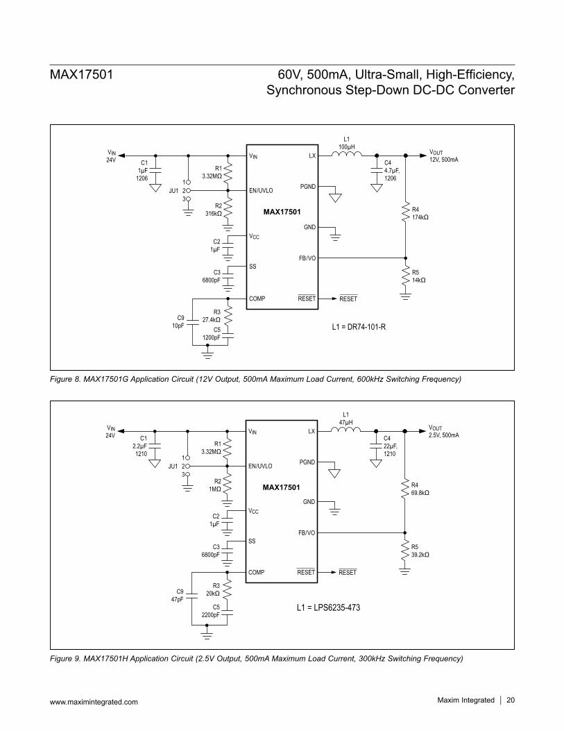
Figure 8. MAX17501G Application Circuit (12V Output, 500mA Maximum Load Current, 600kHz Switching Frequency)
Figure 9. MAX17501H Application Circuit (2.5V Output, 500mA Maximum Load Current, 300kHz Switching Frequency)
C21µF
C36800pF
R327.4kΩ
C51200pF
C910pF
COMP
SS
VCC
EN/UVLO
VIN LX
PGND
GND
FB/VO
RESET
VIN24V C1
1µF1206 1
2JU1
R13.32MΩ
R2316kΩ
3
MAX17501
RESET
L1100µH
C44.7µF,1206
VOUT12V, 500mA
R4174kΩ
R514kΩ
L1 = DR74-101-R
C21µF
C36800pF
R320kΩ
C52200pF
C947pF
COMP
SS
VCC
EN/UVLO
VIN LX
PGND
GND
FB/VO
RESET
VIN24V C1
2.2µF1210 1
2JU1
R13.32MΩ
R21MΩ
3
MAX17501
RESET
L147µH
C422µF,1210
VOUT2.5V, 500mA
R469.8kΩ
R539.2kΩ
L1 = LPS6235-473
MAX17501 60V, 500mA, Ultra-Small, High-Efficiency, Synchronous Step-Down DC-DC Converter
www.maximintegrated.com Maxim Integrated 21
Package InformationFor the latest package outline information and land patterns (footprints), go to www.maximintegrated.com/packages. Note that a “+”, “#”, or “-” in the package code indicates RoHS status only. Package drawings may show a different suffix character, but the drawing pertains to the package regardless of RoHS status.
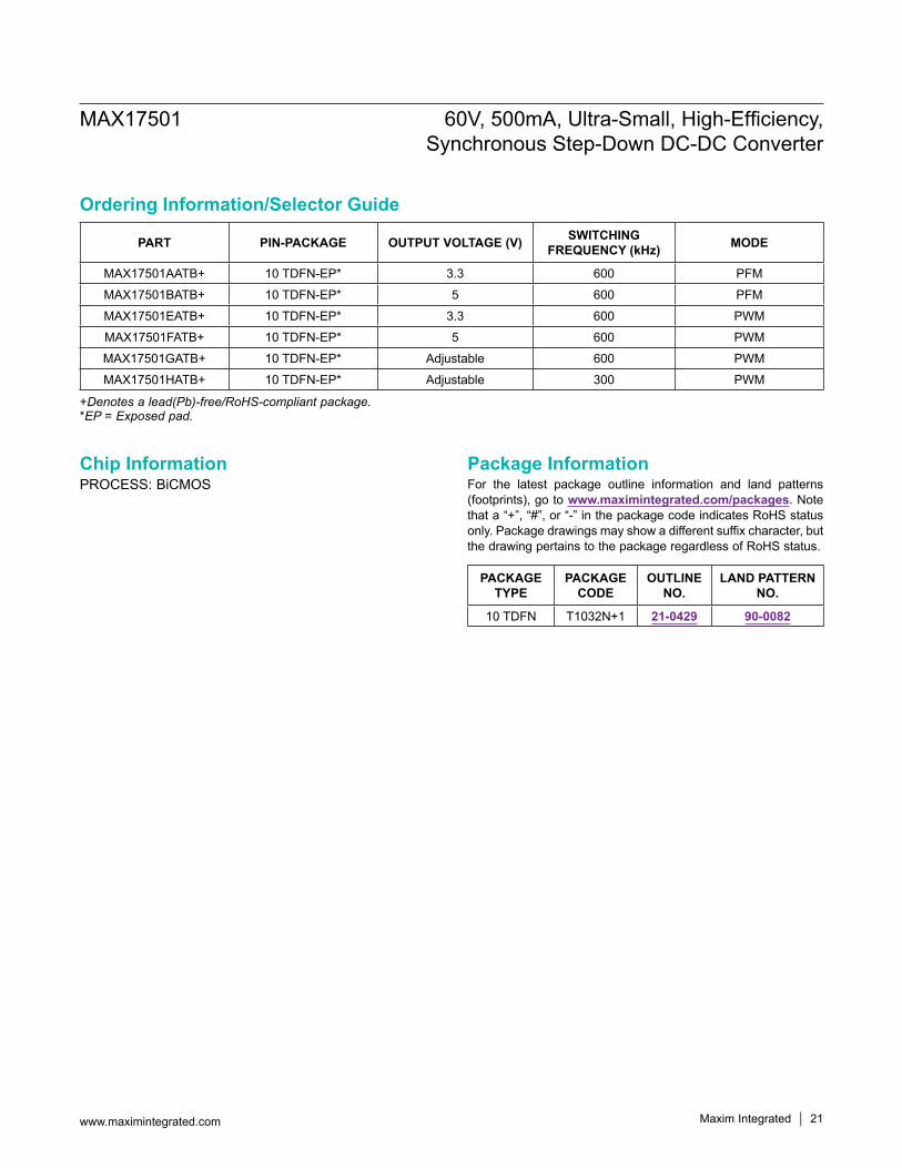
Chip InformationPROCESS: BiCMOS
+Denotes a lead(Pb)-free/RoHS-compliant package. *EP = Exposed pad.
Ordering Information/Selector Guide
PART PIN-PACKAGE OUTPUT VOLTAGE (V) SWITCHING FREQUENCY (kHz) MODE
MAX17501AATB+ 10 TDFN-EP* 3.3 600 PFM
MAX17501BATB+ 10 TDFN-EP* 5 600 PFM
MAX17501EATB+ 10 TDFN-EP* 3.3 600 PWM
MAX17501FATB+ 10 TDFN-EP* 5 600 PWM
MAX17501GATB+ 10 TDFN-EP* Adjustable 600 PWM
MAX17501HATB+ 10 TDFN-EP* Adjustable 300 PWM
PACKAGE TYPE
PACKAGE CODE
OUTLINE NO.
LAND PATTERN NO.
10 TDFN T1032N+1 21-0429 90-0082
Maxim Integrated cannot assume responsibility for use of any circuitry other than circuitry entirely embodied in a Maxim Integrated product. No circuit patent licenses are implied. Maxim Integrated reserves the right to change the circuitry and specifications without notice at any time. The parametric values (min and max limits) shown in the Electrical Characteristics table are guaranteed. Other parametric values quoted in this data sheet are provided for guidance.
Maxim Integrated and the Maxim Integrated logo are trademarks of Maxim Integrated Products, Inc. © 2016 Maxim Integrated Products, Inc. 22
MAX17501 60V, 500mA, Ultra-Small, High-Efficiency, Synchronous Step-Down DC-DC Converter
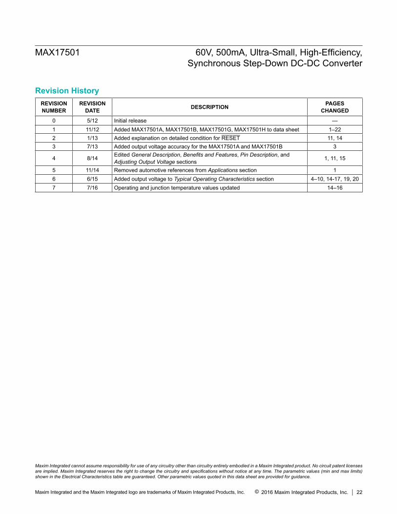
Revision HistoryREVISION NUMBER
REVISION DATE DESCRIPTION PAGES
CHANGED
0 5/12 Initial release —1 11/12 Added MAX17501A, MAX17501B, MAX17501G, MAX17501H to data sheet 1–222 1/13 Added explanation on detailed condition for RESET 11, 143 7/13 Added output voltage accuracy for the MAX17501A and MAX17501B 3
4 8/14 Edited General Description, Benefits and Features, Pin Description, and Adjusting Output Voltage sections 1, 11, 15
5 11/14 Removed automotive references from Applications section 16 6/15 Added output voltage to Typical Operating Characteristics section 4–10, 14-17, 19, 207 7/16 Operating and junction temperature values updated 14–16