A Wide-Bandwidth 2.4GHz ISM Band Fractional-N PLL with...
13
A Wide-Bandwidth 2.4GHz ISM Band Fractional-N PLL with Adaptive Phase Noise Cancellation Ashok Swaminathan 1,2 , Kevin J. Wang 1 , Ian Galton 1 1 University of California, San Diego, CA 2 NextWave Broadband, San Diego, CA 1 Outline • Phase-Noise Canceling Phase-locked loops • Adaptive Phase-Noise Cancellation • Circuits • Experimental Results • Conclusion
Transcript of A Wide-Bandwidth 2.4GHz ISM Band Fractional-N PLL with...
A Wide-Bandwidth 2.4GHz ISM Band Fractional-N PLL with
Adaptive Phase Noise Cancellation
Ashok Swaminathan1,2, Kevin J. Wang1, Ian Galton1
1 University of California, San Diego, CA2 NextWave Broadband, San Diego, CA
1
Outline
• Phase-Noise Canceling Phase-locked loops
• Adaptive Phase-Noise Cancellation
• Circuits
• Experimental Results
• Conclusion
Presented at the 2007 IEEE International Solid-State Circuits Conference
2
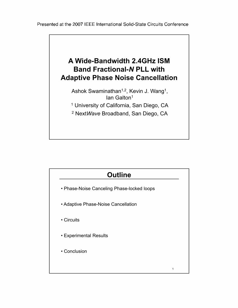
Fractional-N PLL TradeoffPFD and Charge Pump
R
C2
C1
Loop Filter
VCOicp(t)
vctrl(t)ReferenceOscillator
frequency: fref
y[n]Digital '6Modulator
D�
N + y[n]
Digital Logic
frequency: (N+D) fref
dBc/
Hz
Tradeoff: Widening the loop BW greatly increases phase noise:
A pity, because it also:y reduces PLL settling timey reduces sensitivity to VCO pullingy enables an on-chip loop filtery enables in-loop transmit modulation
3
Fractional-N Phase NoisePFD and Charge Pump
R
C2
C1
Loop Filter
icp(t)
vctrl(t)ReferenceOscillator
frequency: fref
y[n]Digital '6Modulator
D�
N + y[n]
Digital Logic
• Each CP pulse is mostly '6quantization noise
Residual '6 noise in vctrl(t):
• But the '6 quantization noise is known, so it can be cancelled with a DAC
4
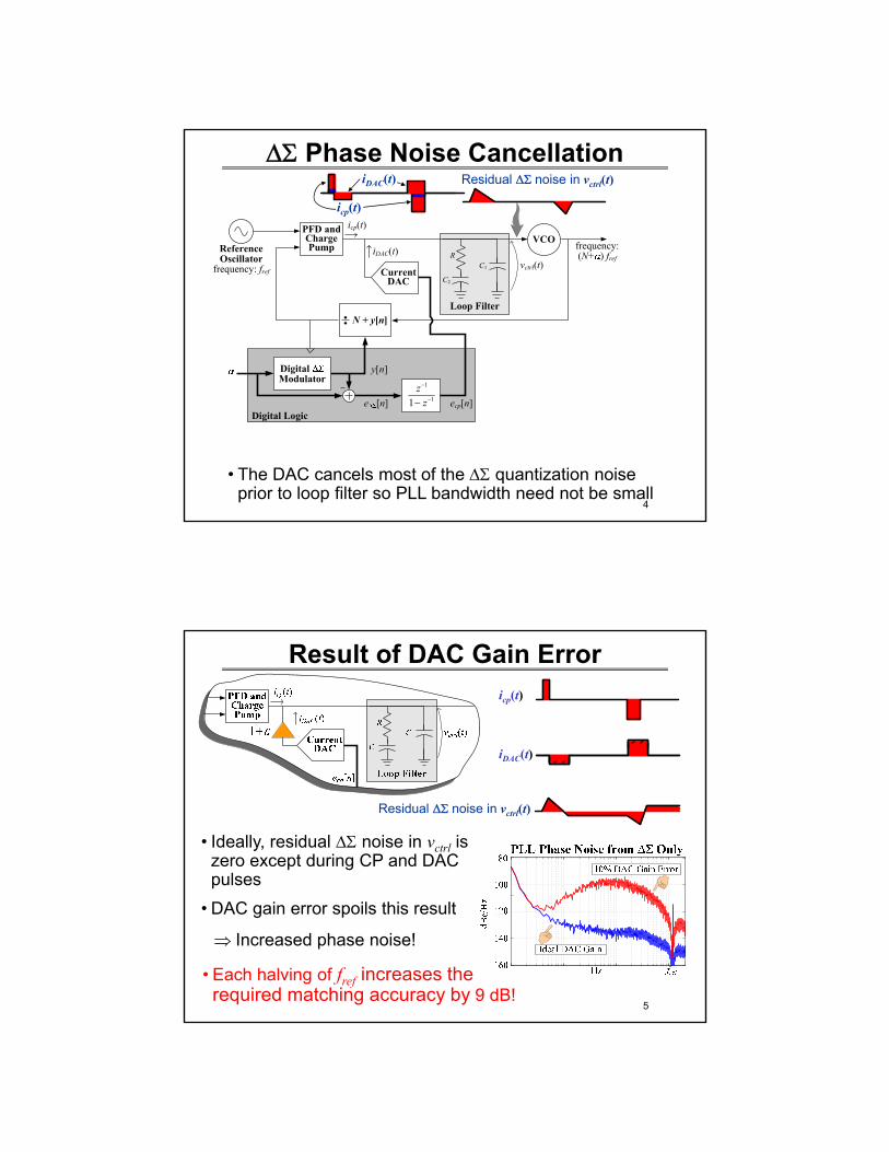
'6 Phase Noise Cancellation
PFD and Charge Pump
R
C2
C1
Loop Filter
VCOicp(t)
vctrl(t)ReferenceOscillator
frequency: fref
y[n]Digital Modulator
N + y[n]
iDAC(t)
Current DAC
1
11z
z
�
��Digital Logic
ecp[n]
frequency: (N+ ) fref
e [n]
icp(t)
iDAC(t) Residual '6 noise in vctrl(t)
• The DAC cancels most of the '6 quantization noise prior to loop filter so PLL bandwidth need not be small
5
Result of DAC Gain Erroricp(t)
iDAC(t)
• Ideally, residual '6 noise in vctrl is zero except during CP and DAC pulses
• DAC gain error spoils this result
� Increased phase noise!
Residual '6 noise in vctrl(t)
• Each halving of fref increases therequired matching accuracy by 9 dB!
6
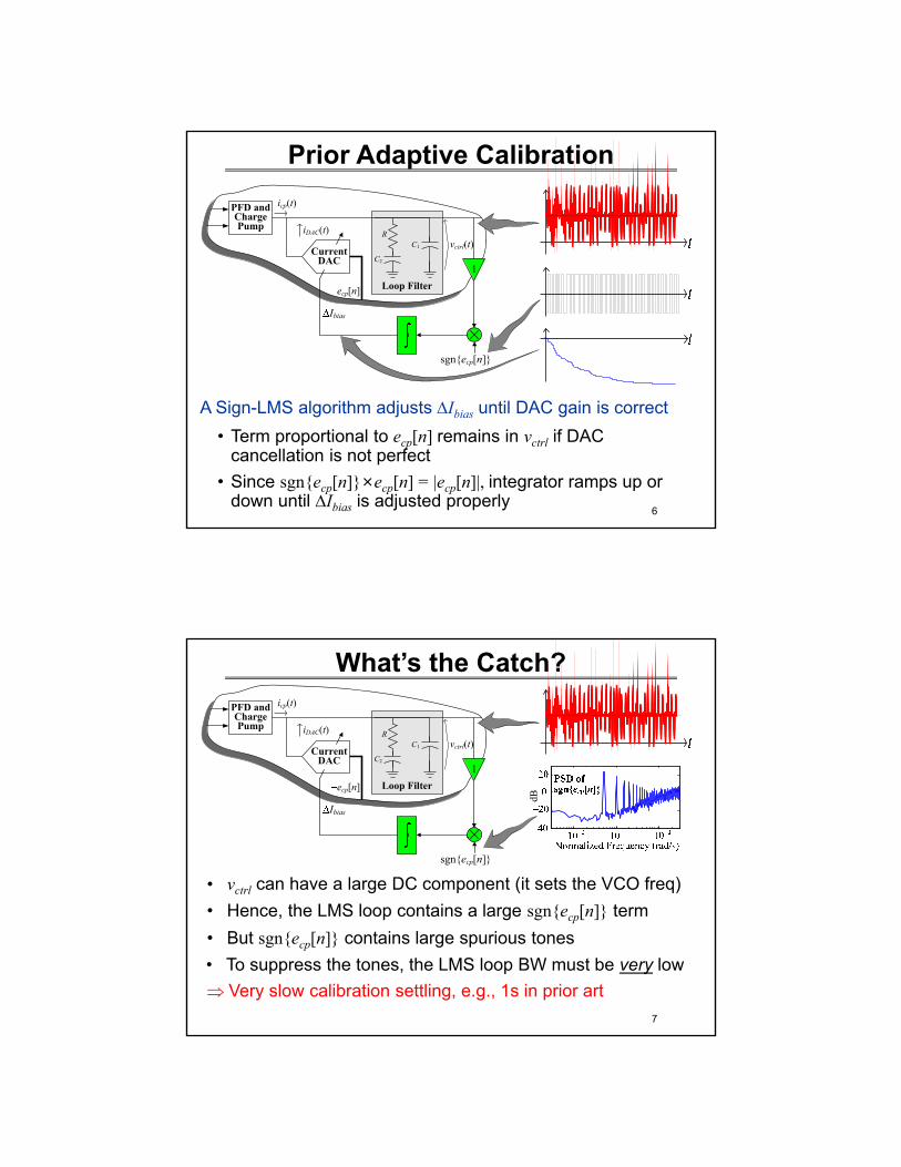
PFD and Charge Pump
R
C2
C1
Loop Filter
icp(t)
vctrl(t)iDAC(t)
Current DAC
ecp[n]
1
sgn{ecp[n]}
Ibias
Prior Adaptive Calibration
A Sign-LMS algorithm adjusts 'Ibias until DAC gain is correct• Term proportional to ecp[n] remains in vctrl if DAC
cancellation is not perfect• Since sgn{ecp[n]}×ecp[n] = |ecp[n]|, integrator ramps up or
down until 'Ibias is adjusted properly
7
What’s the Catch?PFD and Charge Pump
R
C2
C1
Loop Filter
icp(t)
vctrl(t)iDAC(t)
Current DAC
ecp[n]
• Hence, the LMS loop contains a large sgn{ecp[n]} term
1
sgn{ecp[n]}
Ibias
• vctrl can have a large DC component (it sets the VCO freq)
• But sgn{ecp[n]} contains large spurious tones
� Very slow calibration settling, e.g., 1s in prior art
dB
• To suppress the tones, the LMS loop BW must be very low
8
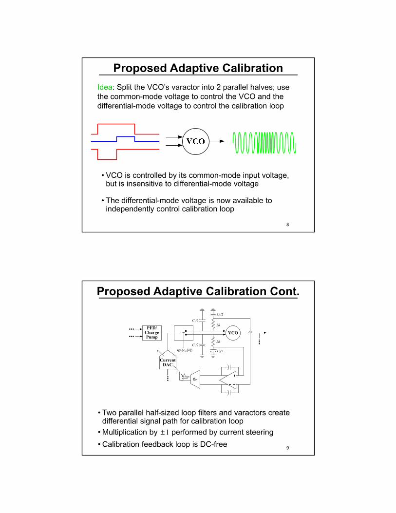
Proposed Adaptive Calibration
• VCO is controlled by its common-mode input voltage, but is insensitive to differential-mode voltage
• The differential-mode voltage is now available to independently control calibration loop
Idea: Split the VCO’s varactor into 2 parallel halves; use the common-mode voltage to control the VCO and the differential-mode voltage to control the calibration loop
9
Proposed Adaptive Calibration Cont.
VCOPFD/
Charge Pump
Current DAC
sgn{ecp[n]}
Ibias gm
2R
C2/2
C1/2
2R
C2/2
C1/2
• Two parallel half-sized loop filters and varactors create differential signal path for calibration loop
• Multiplication by ±1 performed by current steering• Calibration feedback loop is DC-free
10
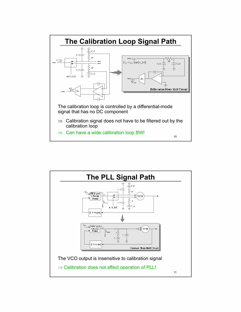
The Calibration Loop Signal Path
� � ^ `sgn [ ]cp DAC cpi i e n�
sgn{ecp[n]}
Ibias gm
2R
C2/2
C1/2
2R
C2/2
C1/2
icp+iDAC
The calibration loop is controlled by a differential-mode signal that has no DC component
� Calibration signal does not have to be filtered out by the calibration loop
� Can have a wide calibration loop BW!
11
The PLL Signal Path
The VCO output is insensitive to calibration signal
� Calibration does not affect operation of PLL!
12
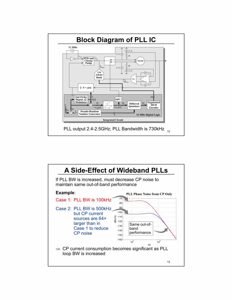
Block Diagram of PLL IC
Dithered Quantizer
Pseudo-Random Number Generator 8
1
1
11z
z
�
��
N + y[n]
Integrated Circuit
2nd-OrderDigital Modulator
12 MHz
VCOPFD and Charge Pump
1-bI-DAC Bank
Ibias
icp
iDAC
gm
C2/2C1/2
2R
C2/2C1/2
2R
y[n]
ecp[n]e [n]16
19sgn{ }
18 10
26
12 MHz Digital Logic
Segmented DEM
Encoder16
3
vref
PLL output 2.4-2.5GHz; PLL Bandwidth is 730kHz
13
A Side-Effect of Wideband PLLsIf PLL BW is increased, must decrease CP noise to maintain same out-of-band performance
Example:
104 106-160
-150
-140
-130
-120
-110
-100
-90
-80
-70
dBc/
Hz
Hz
PLL Phase Noise from CP Only
Case 1: PLL BW is 100kHz
Case 2: PLL BW is 500kHz but CP current sources are 64×larger than in Case 1 to reduce CP noise
� CP current consumption becomes significant as PLL loop BW is increased
Same out-of-band performance
14
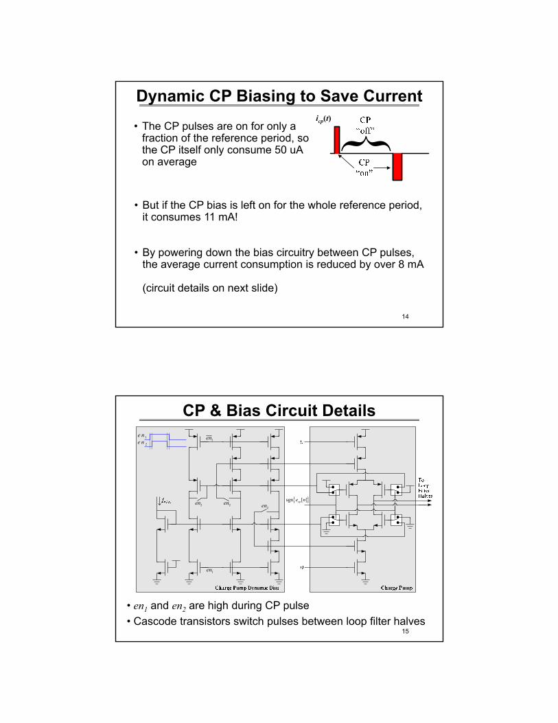
Dynamic CP Biasing to Save Currenticp(t)• The CP pulses are on for only a
fraction of the reference period, so the CP itself only consume 50 uA on average
• But if the CP bias is left on for the whole reference period, it consumes 11 mA!
• By powering down the bias circuitry between CP pulses, the average current consumption is reduced by over 8 mA
(circuit details on next slide)
15
CP & Bias Circuit Details
• en1 and en2 are high during CP pulse• Cascode transistors switch pulses between loop filter halves
^ `sgn [ ]cpe n2en2en
1en
2en
1en
2e n1e n
16
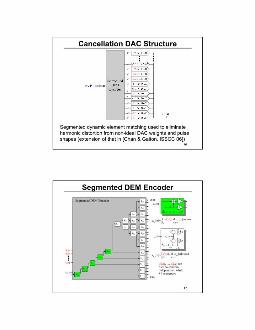
Cancellation DAC Structure
Segmented dynamic element matching used to eliminate harmonic distortion from non-ideal DAC weights and pulse shapes (extension of that in [Chan & Galton, ISSCC 06])
17
Segmented DEM EncoderSegmented DEM Encoder
S1,13
S1,12
S1,11
S1,10
S1,9
S6,1
S7,1
S8,1
S9,1
sk,1[n] ��
1/2
Sk, 1 : k = 5, 6, ..., 9
xk,1[n]
d1[n]d2[n]
d9[n] d1[n], ..., d9[n] are pseudo-random independent, white ±1 sequences
S5,1
S4,1
S3,2
S3,1 S2,2
S2,1
S2,4
S2,3
S1,2
S1,1
S1,4
S1,3
S1,6
S1,5
S1,8
S1,7
LSB
MSB
xk, r[n]
1/2
sk,r[n]
1/2Sk, r : k = 1, ...,4,
r = 1, ..., 13
xDAC[n]
,1,1
1 , if [ ] even[ ] 1[ ]
, elsek k
kd xn n nq
°®°̄
�
,,
, if [ ] odd[ ] 0, else[ ]k k r
k rx ns n d n°
®°̄
18
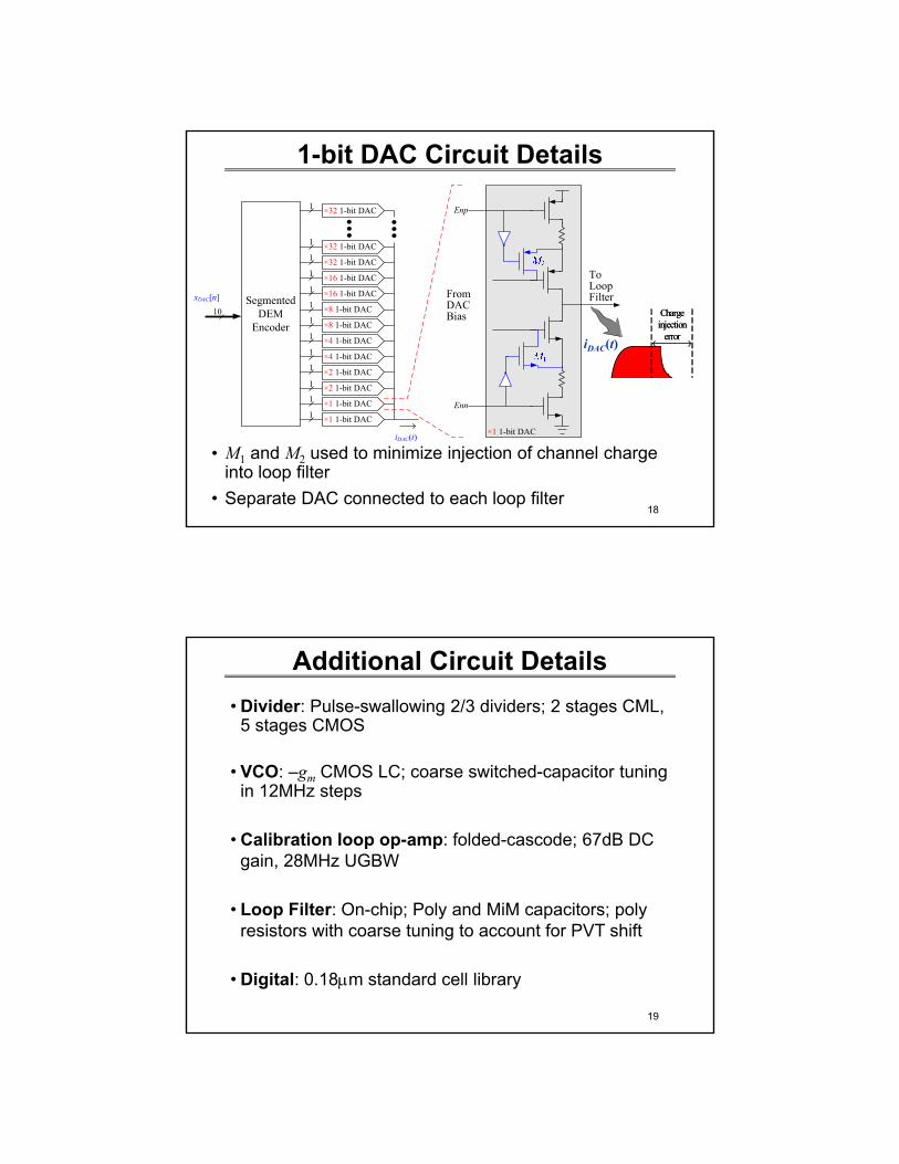
1-bit DAC Circuit Details
Enp
To Loop FilterFrom
DAC Bias
iDAC(t)
1
1 ×32 1-bit DAC1
1 ×16 1-bit DAC1 ×16 1-bit DAC1 ×8 1-bit DAC1 ×8 1-bit DAC1 ×4 1-bit DAC1 ×4 1-bit DAC1 ×2 1-bit DAC1 ×2 1-bit DAC1 ×1 1-bit DAC1 ×1 1-bit DAC
Segmented DEM
Encoder
×32 1-bit DAC
×32 1-bit DAC
10xDAC[n]
Enn
×1 1-bit DAC
• M1 and M2 used to minimize injection of channel charge into loop filter
• Separate DAC connected to each loop filter
Charge injection
erroriDAC(t)
Charge injection
error
19
Additional Circuit Details• Divider: Pulse-swallowing 2/3 dividers; 2 stages CML,
5 stages CMOS
• VCO: –gm CMOS LC; coarse switched-capacitor tuning in 12MHz steps
• Calibration loop op-amp: folded-cascode; 67dB DC gain, 28MHz UGBW
• Loop Filter: On-chip; Poly and MiM capacitors; poly resistors with coarse tuning to account for PVT shift
• Digital: 0.18Pm standard cell library
20
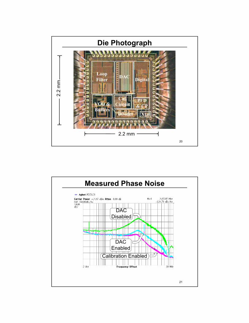
Die Photograph
2.2 mm
2.2
mm
Loop Filter DAC Digital
Cal.Circuit
Divider
VCO & Buffers
PFD & CP
Xtal
21
Measured Phase Noise
Calibration Enabled
DAC Disabled
DAC Enabled
22
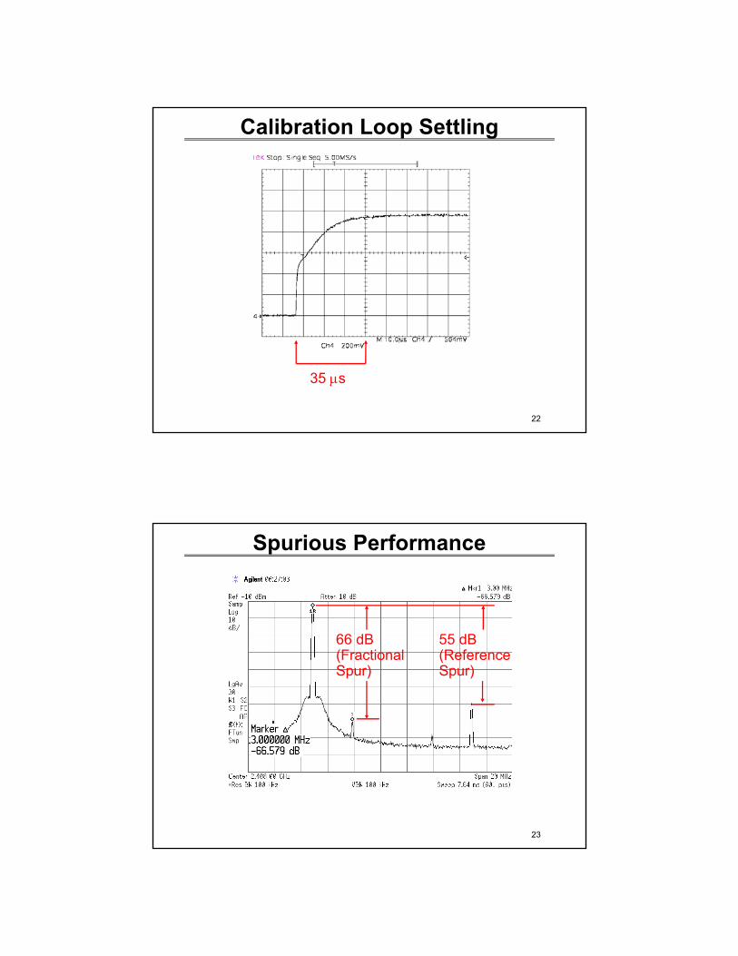
Calibration Loop Settling
35 Ps
23
Spurious Performance
55 dB (Reference Spur)
66 dB (Fractional Spur)
24
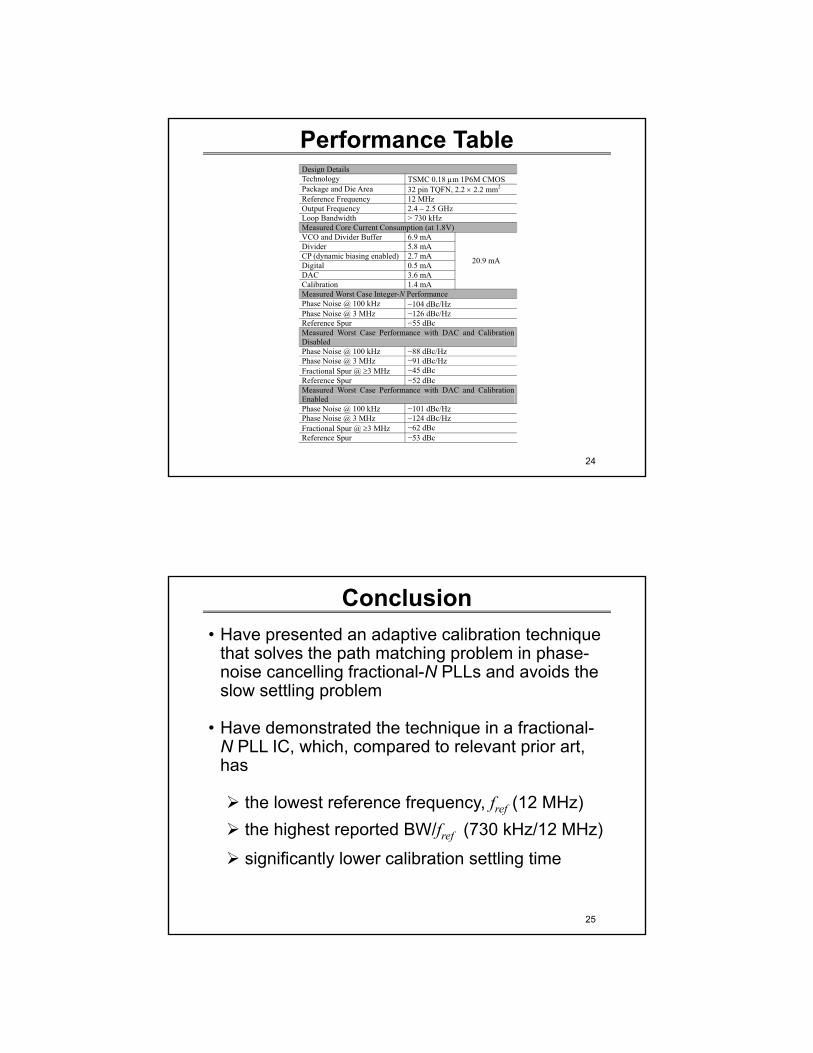
Performance TableDesign Details Technology TSMC 0.18 Pm 1P6M CMOS Package and Die Area 32 pin TQFN, 2.2 u 2.2 mm2 Reference Frequency 12 MHz Output Frequency 2.4 – 2.5 GHz Loop Bandwidth > 730 kHz Measured Core Current Consumption (at 1.8V) VCO and Divider Buffer 6.9 mA Divider 5.8 mA CP (dynamic biasing enabled) 2.7 mA Digital 0.5 mA DAC 3.6 mA Calibration 1.4 mA
20.9 mA
Measured Worst Case Integer-N Performance Phase Noise @ 100 kHz �104 dBc/Hz Phase Noise @ 3 MHz −126 dBc/Hz Reference Spur −55 dBc Measured Worst Case Performance with DAC and Calibration Disabled Phase Noise @ 100 kHz −88 dBc/Hz Phase Noise @ 3 MHz −91 dBc/Hz Fractional Spur @ t3 MHz −45 dBc Reference Spur −52 dBc Measured Worst Case Performance with DAC and Calibration Enabled Phase Noise @ 100 kHz −101 dBc/Hz Phase Noise @ 3 MHz −124 dBc/Hz Fractional Spur @ t3 MHz −62 dBc Reference Spur −53 dBc
25
Conclusion• Have presented an adaptive calibration technique
that solves the path matching problem in phase-noise cancelling fractional-N PLLs and avoids the slow settling problem
• Have demonstrated the technique in a fractional-N PLL IC, which, compared to relevant prior art, has
¾ the lowest reference frequency, fref (12 MHz)¾ the highest reported BW/fref (730 kHz/12 MHz)¾ significantly lower calibration settling time


![LM842 WiFi 802.11ac / Bluetooth® 5.0 2T2R USB Combi ... · 2.4 GHz and 5GHz ISM Frequency bands 2T2R 802.11n 2.4GHz WiFi 300Mbps data rate [Untested] 2T2R 802.11ac 5GHz WiFi 867Mbps](https://static.fdocuments.in/doc/165x107/5e3ec26237dff24e794e8541/lm842-wifi-80211ac-bluetooth-50-2t2r-usb-combi-24-ghz-and-5ghz-ism-frequency.jpg)