A VLSI Sorting Image Sensor: Global Massively … TRANSACTIONS ON ROBOTICS AND AUTOMATION, VOL. 15,...
9
IEEE TRANSACTIONS ON ROBOTICS AND AUTOMATION, VOL. 15, NO. 1, FEBRUARY 1999 67 A VLSI Sorting Image Sensor: Global Massively Parallel Intensity-to-Time Processing for Low-Latency Adaptive Vision Vladimir Brajovic, Member, IEEE, and Takeo Kanade, Fellow, IEEE Abstract—This paper presents a new intensity-to-time process- ing paradigm suitable for very large scale integration (VLSI) computational sensor implementation of global operations over sensed images. Global image quantities usually describe images with fewer data. When computed at the point of sensing, global quantities result in a low-latency performance due to the reduced data transfer requirements between an image sensor and a processor. The global quantities also help global top-down adap- tation: the quantities are continuously computed on-chip, and are readily available to sensing for adaptation. As an example, we have developed a sorting image computational sensor—a VLSI chip which senses an image and sorts all pixel by their intensities. The first sorting sensor prototype is a 21 26 array of cells. It receives an image optically, senses it, and computes the image’s cumulative histogram—a global quantity which can be quickly routed off chip via one pin. In addition, the global cumulative histogram is used internally on-chip in a top-down fashion to adapt the values in individual pixel so as to reflect the index of the incoming light, thus computing an “image of indices.” The image of indices never saturates and has a uniform histogram. Index Terms— Computational sensors, image sensors, robot perception, smart sensors, vision, VLSI sensors. I. INTRODUCTION M ANY time-critical robotics applications, such as au- tonomous vehicles and human-machine interfaces, need a low-latency and adaptable vision system. Conventional vision systems comprised of a camera and processor provide neither low-latency performance nor sufficient adaptation. Latency is the time that a system takes to react to an event. In the conventional systems, the latency is incurred in both the data transfer bottleneck created by the separation of the camera and the processor and in the computational load bottleneck created by the necessity to process a huge amount of image data. For example, a standard video camera takes 1/30 of a second to transfer an image. In many critical applications, the image capture alone presents excessive latency for the stable control of a robotics system. Another example is the pipeline dedicated vision hardware which delivers the processing power to update its output 30 times per second; however, the latency Manuscript received July 23, 1997; revised June 3, 1998. This work was supported in part by ONR Grant N00014-95-1-0591 and NSF Grant MIP- 9305494. This paper was recommended for publication by Associate Editor S. Hutchinson and Editor A. Goldenberg upon evaluation of the reviewers comments. The authors are with the Robotics Institute, Carnegie Mellon University, Pittsburgh, PA 15213 USA (e-mail: [email protected]). Publisher Item Identifier S 1042-296X(99)01326-9. through the pipeline is typically several frame times, again rendering the conventional system unsuitable for many time- critical applications. The second important feature of a vision system is adap- tation. It has been repeatedly observed in machine vision research that using the most appropriate sensing modality or setup, allows algorithms to be far more simple and reliable. For example, the concept of active vision proposes to control the geometric parameters of the camera (e.g., pan, tilt, zoom, etc.) to improve the reliability of the perception. It has been shown that initially ill-posed problems can be solved after the top- down adaptation of the camera’s pose has acquired new, more appropriate image data [1]. Adjusting geometric parameters is only one level where adaptation can take place. A system which can adjust its operations at all levels, even down to the point of sensing, would be far more adaptive than the one that tries to cope with the variations at the “algorithmic” or “motoric” level alone. The computational sensor paradigm [3], [11] has potential to greatly reduce latency and provide adaptation. By integrating sensing and processing on a very large scale integration (VLSI) chip, both transfer and computational bottlenecks can be alleviated: on-chip routing provides high throughput transfer, while an on-chip processor could implement massively parallel computational models. Adaptation is also more conveniently facilitated: the results of processing are readily available to sensing for adaptation. So far, a great majority of computational sensory solutions implement local operations on a single light sensitive VLSI chip (for examples, see [11], [13], and [19]). Local operations use operands within a small spatial/temporal neighborhood of data and, thus, lend themselves to graceful implementation in VLSI. Typical examples include filtering and motion com- putation. Local operations produce preprocessed “images;” therefore, a large quantity of data still must be read out and further inspected before a decision for an appropriate action is made—usually a time-consuming process. Locally computed quantities could be used for adaptation within the local neighborhood, but not globally. Consequently, a great majority of computational sensors built thus far are limited in their ability to quickly respond to changes in the environment and to globally adapt to a new situation. Global operations, on the other hand, produce fewer quan- tities for the description of the environment. An image his- togram is an example of a global image descriptor. If computed 1042–296X/99$10.00 1999 IEEE
Transcript of A VLSI Sorting Image Sensor: Global Massively … TRANSACTIONS ON ROBOTICS AND AUTOMATION, VOL. 15,...

IEEE TRANSACTIONS ON ROBOTICS AND AUTOMATION, VOL. 15, NO. 1, FEBRUARY 1999 67
A VLSI Sorting Image Sensor: Global MassivelyParallel Intensity-to-Time Processing
for Low-Latency Adaptive VisionVladimir Brajovic, Member, IEEE,and Takeo Kanade,Fellow, IEEE
Abstract—This paper presents a new intensity-to-time process-ing paradigm suitable for very large scale integration (VLSI)computational sensor implementation of global operations oversensed images. Global image quantities usually describe imageswith fewer data. When computed at the point of sensing, globalquantities result in a low-latency performance due to the reduceddata transfer requirements between an image sensor and aprocessor. The global quantities also help global top-down adap-tation: the quantities are continuously computed on-chip, and arereadily available to sensing for adaptation. As an example, wehave developed a sorting image computational sensor—a VLSIchip which senses an image and sorts all pixel by their intensities.The first sorting sensor prototype is a 21��� 26 array of cells. Itreceives an image optically, senses it, and computes the image’scumulative histogram—a global quantity which can be quicklyrouted off chip via one pin. In addition, the global cumulativehistogram is used internally on-chip in a top-down fashion toadapt the values in individual pixel so as to reflect the index ofthe incoming light, thus computing an “image of indices.” Theimage of indices never saturates and has a uniform histogram.
Index Terms—Computational sensors, image sensors, robotperception, smart sensors, vision, VLSI sensors.
I. INTRODUCTION
M ANY time-critical robotics applications, such as au-tonomous vehicles and human-machine interfaces, need
a low-latency and adaptable vision system. Conventionalvision systems comprised of a camera and processor provideneither low-latency performance nor sufficient adaptation.
Latency is the time that a system takes to react to an event.In the conventional systems, the latency is incurred in both thedata transfer bottleneck created by the separation of the cameraand the processor and in the computational load bottleneckcreated by the necessity to process a huge amount of imagedata. For example, a standard video camera takes 1/30 of asecond to transfer an image. In many critical applications, theimage capture alone presents excessive latency for the stablecontrol of a robotics system. Another example is the pipelinededicated vision hardware which delivers the processing powerto update its output 30 times per second; however, the latency
Manuscript received July 23, 1997; revised June 3, 1998. This work wassupported in part by ONR Grant N00014-95-1-0591 and NSF Grant MIP-9305494. This paper was recommended for publication by Associate EditorS. Hutchinson and Editor A. Goldenberg upon evaluation of the reviewerscomments.
The authors are with the Robotics Institute, Carnegie Mellon University,Pittsburgh, PA 15213 USA (e-mail: [email protected]).
Publisher Item Identifier S 1042-296X(99)01326-9.
through the pipeline is typically several frame times, againrendering the conventional system unsuitable for many time-critical applications.
The second important feature of a vision system is adap-tation. It has been repeatedly observed in machine visionresearch that using the most appropriate sensing modality orsetup, allows algorithms to be far more simple and reliable. Forexample, the concept of active vision proposes to control thegeometric parameters of the camera (e.g., pan, tilt, zoom, etc.)to improve the reliability of the perception. It has been shownthat initially ill-posed problems can be solved after the top-down adaptation of the camera’s pose has acquired new, moreappropriate image data [1]. Adjusting geometric parametersis only one level where adaptation can take place. A systemwhich can adjust its operations at all levels, even down tothe point of sensing, would be far more adaptive than the onethat tries to cope with the variations at the “algorithmic” or“motoric” level alone.
The computational sensor paradigm [3], [11] has potential togreatly reduce latency and provide adaptation. By integratingsensing and processing on a very large scale integration (VLSI)chip, both transfer and computational bottlenecks can bealleviated: on-chip routing provides high throughput transfer,while an on-chip processor could implement massively parallelcomputational models. Adaptation is also more convenientlyfacilitated: the results of processing are readily available tosensing for adaptation.
So far, a great majority of computational sensory solutionsimplement local operationson a single light sensitive VLSIchip (for examples, see [11], [13], and [19]). Local operationsuse operands within a small spatial/temporal neighborhood ofdata and, thus, lend themselves to graceful implementationin VLSI. Typical examples include filtering and motion com-putation. Local operations produce preprocessed “images;”therefore, a large quantity of data still must be read outand further inspected before a decision for an appropriateaction is made—usually a time-consuming process. Locallycomputed quantities could be used for adaptation within thelocal neighborhood, but not globally. Consequently, a greatmajority of computational sensors built thus far are limited intheir ability to quickly respond to changes in the environmentand to globally adapt to a new situation.
Global operations,on the other hand, produce fewer quan-tities for the description of the environment. An image his-togram is an example of a global image descriptor. If computed
1042–296X/99$10.00 1999 IEEE

68 IEEE TRANSACTIONS ON ROBOTICS AND AUTOMATION, VOL. 15, NO. 1, FEBRUARY 1999
at the point of sensing, global quantities can be routed offa computational sensor through a few output pins withoutcausing a transfer bottleneck. In many applications, this infor-mation will often be sufficient for rapid decision making andthe actual image does not need to be read out. The computedglobal quantities also can be used in top-down fashion toupdate localand globalproperties of the system for adaptingto new conditions in the environment. Implementing globaloperations in hardware, however, is not trivial. The main diffi-culty comes from the necessity to bring together, or aggregate,all or most of the data in the input data set [3], [5]. Thisglobal exchange of data among a large number of processorsquickly saturates communication connections and adverselyaffects computing efficiency in parallel systems—parallel dig-ital computers and computational sensors alike. It is notsurprising that there are only a few computational sensors forglobal operations: [8] and [18] show computational sensors fordetecting isolated bright objects against the dark backgroundand computing the object’s position and orientation, and [6]and [16] show attention-based computational sensors thatglobally select the “most salient features” across the array ofphotoreceptors.
This work introduces a novel intensity-to-time processingparadigm—an efficient solution for VLSI implementation oflow-latency massively parallelglobal computation over largegroups of fine-grained data. By using this paradigm, we havedeveloped a sorting computational sensor—an analog VLSIchip which sorts pixel of a sensed image by their intensities.The sorting sensor producesimages of indicesthat neversaturate. As a by-product, the chip provides a cumulativehistogram—a global descriptor of the scene—on one of thepins; this histogram can be used for low-latency decisionmaking before the image is read out.
II. I NTENSITY-TO-TIME PROCESSINGPARADIGM
The intensity-to-time processing paradigm implementsglobal operations by aggregating only a few of the input dataat a time. Inspired by biological vision [20], the paradigm isbased on the notion that stronger input signals elicit responsesbefore weaker ones. Assuming that the inputs have differentintensities, the intensity-to-time paradigm separates responsesin time allowing a global processor to makes decisions basedonly on a few inputs at a time. The more time allowed,the more responses are received; thus, the global processorincrementally builds a global decision first based on several,and eventually based on all, the inputs. The key is thatsome preliminary decision about the environment can bemade as soon as the first responses are received. Therefore,this paradigm has an important place in low-latency visionprocessing.
The architecture supporting intensity-to-time processing isshown in Fig. 1. After a common reset signal at 0, a cell
generates an event at the instant
(1)
where is a monotonic function, and the radiationreceived by the cell . Therefore, any two cells receiving
Fig. 1. A computational sensor architecture for the intensity-to-time pro-cessing paradigm.
radiation of different magnitude generate events at differenttimes. If is decaying, then the ordering of events isconsistent with a biological system: stronger stimuli elicitresponses before weaker ones.
A global processor receives and processes events. In ad-dition, there can be a local processor attached to each cell.The generated events then control the instant when a localprocessor in each cell performs at least one predetermined(i.e., prewired or preprogrammed) operation. By separating theinput data in time, the intensity-to-time processing paradigmeases the global data aggregation and computation:
1) global processor processes only a few events at a time;2) communication resources are shared by many cells;3) global processor and local processors infer the input
operand intensity by measuring the time an event isreceived [e.g., ].
Traditionally, the intensity-to-time relationship has beenused in single and double slope A/D converters [10]. Invision, it has been used to improve diffusion-based imagesegmentation [7]—a local operation, and for image acquisitionin a SIMD architecture [9]—an architecture well suited onlyfor local operations. In contrast, our architecture allows globaloperations and shares some features of traditional MIMDparallel processing. Namely, the local processors perform theiroperationsasynchronously,an essential feature for the quickresponse and the low latency performance of parallel systems[3].
The intensity-to-time is closely related to the event-addressneural communication schemes proposed by a number ofresearchers [12], [15], [17]. In these schemes the pluralityof artificial neurons fire pulses (i.e.,events) at rates re-flecting their individual levels of activity. The goal is to

BRAJOVIC AND KANADE: VLSI SORTING IMAGE SENSOR 69
communicate this activity to other neurons or to an outputdevice. The event-address scheme shares communication wiresby communicating the identity (i.e.,address) of the neuronwhen it fires a pulse. Since the time is inherently measuredacross the entire system, the receiver recovers the firing ratefor each transmitting neuron. The intensity-to-time paradigmsynchronizes the responses at the beginning of operations anddeals with the time intervals each “neuron” takes to fire itsfirst pulse.
III. SORTING IMAGE SENSOR CHIP
By using the intensity-to-time paradigm, we have developeda sorting computational sensor—an analog VLSI sensor whichsorts the pixel of an input image by their intensities. The chipdetects an image focused thereon and computes animage ofindices.The image of indices has a uniform histogram whichhas several important properties:
1) contrast is maximally enhanced;2) available dynamic range of readout circuitry is equally
utilized, i.e., the values read out from the chip useavailable bits most efficiently;
3) image of indices never saturates, and always preservesthe same range (e.g., from 1 to, where is thenumber of pixel).
During the computation, the chip computes a cumulativehistogram—one global descriptor of the detected scene—andreports it with low-latency on one of the pins. In fact, theglobal cumulative histogram is used in top-down fashion toupdate information in local processors and produce the imageof indices.
The sorting operation is accomplished in the following way.The plurality of cells detect light and generate events accordingto (1), where is decaying function. Cells receiving morelight generate events before cells receiving less light. Theglobal processor counts the events generated within the array.Since the intensities are ordered in time, the count representsthe order, or index, of the cell that is generating an event next.For example, if events were already generated at the instanta cell generates the event, the order of the cellis . Therefore, the sorting is done by associating the cell(s)currently generating an event with the current count producedby the global counter.
Fig. 2 shows the circuit of the sorting sensor. The globalprocessor/counter comprises an array of constant currentsources , a current-to-voltage converter (resistor), avoltage follower, and wires and . Upon the arrivalof the event generated by a cell, the corresponding individualcurrent source is turned on via switch . The currentsources are summed in the wire . The cumulative currentin the wire continuously reports the number of cellsthat have responded with an event—the global count. Thecumulative current is converted to a voltage via resistor,and fed in a top-down fashion to the local processors in thecell array via wire .
The local processor in each cell comprises a track-and-hold(T/H) circuit. The T/H tracks the voltage on until theevent in the cell is generated. At that point the local processors
Fig. 2. Schematic diagram of the sorting computational sensor.
Fig. 3. Sorting computational sensor: a four cell simulated operation.
remember voltage supplied by the global counter on the wire. Thus, the appropriate index is assigned to each cell.
The remaining portion of the cell comprises the photosensitive intensity-to-time event generator which generatesan event according to (1). Fig. 3 shows the simulation ofthe circuit operation for the sorting sensor with four cells.A photodiode operating in the photon flux integratingmode [21] detects the light. In this mode of operation thecapacitance of the diode is charged to a high potential andleft to float. Since the diode capacitance is discharged by the

70 IEEE TRANSACTIONS ON ROBOTICS AND AUTOMATION, VOL. 15, NO. 1, FEBRUARY 1999
photo current, the voltage decreases approximately linearly ata rate proportional to the amount of light impinging on thediode (Fig. 3, top graph).
The diode voltage is monitored by a CMOS inverter. Oncethe diode voltage falls to the threshold of the inverter, theinverter’s output changes state from low to high (Fig. 3,second graph). A switch is included to provide a positivefeed back and force rapid latching action. The transition inthe output of the inverter represents the event generated bythe cell. It controls theinstant when the capacitor in theT/H memorizes the voltage supplied on the wire . It alsocontrols the instant when the currentis supplied to the wire
.The voltage on the wire (Fig. 3, third graph) represents
the index of a cell that is changing state and is supplied to theglobal input wire. The T/H within each cell follows this voltageuntil it is disconnected, at which point a capacitorretainsthe index of the cell (Fig. 3, bottom graph). The bottom graphshows that the cell with the highest intensity input has receivedthe highest “index,” the next cell one “index” lower, and soon. The charge from the capacitors is readout by scanning thearray after all the cells responded or after a predeterminedtime-out.
The sorting sensor computes several important propertiesabout the image focused thereon. First, the time when a cell
triggers is approximately inversely proportional to the inputradiation it receives
(2)
where is the diodes capacitance, the power supplyvoltage, the threshold voltage of the inverter, andphotocurrent approximately proportional to the radiation, andisthe dark current.
Second, by summing up the currents, the global processorknows at each given time how many cells have respondedwith an event. Since events are generated according to (1),the cumulative current in the wire , or its inverse, thevoltage on the wire , are recognized as being temporalrepresentations of the cumulative histogram of the input data,with the horizontal axis being proportional to . The timederivative of the cumulative histogram signal is related to ahistogram of the input image [2]. The cumulative histogramis one global property of the scene that is reported by thechip with very low latency. Such information can be used forpreliminary decision making as soon as the first responses arereceived. In fact, it is used on-chip to quickly adapt indexvalues for every new frame of input data.
IV. VLSI REALIZATION AND EVALUATION
A 21 26 cell sorting sensor has been built in 2CMOStechnology. The size of each cell is 76 90 , with 13%fill factor. The micrograph of the chip is shown in Fig. 4. Animage was focused directly onto the silicon. The cumulativehistogram waveform as well as the indices from the sortingsensor were digitized with 12-bit resolution.
Scene 1 of an office environment was imaged by thesorting chip under common office illumination coming from
Fig. 4. Micrograph of the sorting chip.
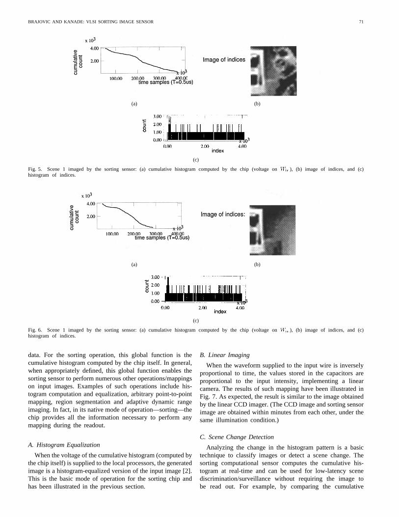
the ceiling. Fig. 5(a) and (b) shows the cumulative histogramof the sceneand the image of indices both computed by thechip. We evaluated the histogram of the indices which is shownin Fig. 5(c). From Fig. 5(c) it is seen that most pixel appearedto have different input intensities and, therefore, receiveddifferent indices. Occasionally, as many as three pixel wereassigned the same index. Overall, the histogram of indicesis uniform, indicating that the sorting chip has performedcorrectly.
Scene 2 from the same office was also imaged. Scene 1(Fig. 5) contains more dark regions than Scene 2 (Fig. 6)because the moderately bright wall in the background isreplaced by the dark regions of the person in partial shadow.Therefore, the chip takes longer to compute Scene 1 than Scene2, but the dynamic range of the output indices is maintained.The total time shown on the time sample axis of the cumulativehistograms is about 200 ms.
By producing the cumulative histogram waveform and theimage of indices, the sorting computational sensor providesall the necessary information for the inverse mapping—themapping from the indices to the input intensities. Fig. 7(a)shows the image of indices for Scene 1 and the image ofinferred input intensities. Fig. 7(b) includes an image takenby a commercial CCD camera for showing natural lightconditions in the office environment from which Scene 1was taken. The inferred input intensities closely resemble thenatural low contrast conditions in the environment.
There is a total of 546 pixel in the prototype described inthis paper. The uniform histogram of indices [Figs. 5(c) and6(c)] indicates that most of the pixel received different indices.Therefore, without special considerations as to the illuminationconditions, low-noise circuit design and temperature and darkcurrent control, our lab prototype readily provides indiceswith more than 9 b of resolution. Furthermore, the range ofindices remains unchanged (from 0 to 545) and the indicesmaintain uniform histogram regardless of the range of inputlight intensity or its histogram.
V. SORTING SENSOR IMAGE PROCESSING
The data that are stored in the local processors are providedby the global processor. These global data—a function oftime—define a mapping from the input intensities to output
BRAJOVIC AND KANADE: VLSI SORTING IMAGE SENSOR 71
(a) (b)
(c)
Fig. 5. Scene 1 imaged by the sorting sensor: (a) cumulative histogram computed by the chip (voltage onWin), (b) image of indices, and (c)histogram of indices.
(a) (b)
(c)
Fig. 6. Scene 1 imaged by the sorting sensor: (a) cumulative histogram computed by the chip (voltage onWin), (b) image of indices, and (c)histogram of indices.
data. For the sorting operation, this global function is thecumulative histogram computed by the chip itself. In general,when appropriately defined, this global function enables thesorting sensor to perform numerous other operations/mappingson input images. Examples of such operations include his-togram computation and equalization, arbitrary point-to-pointmapping, region segmentation and adaptive dynamic rangeimaging. In fact, in its native mode of operation—sorting—thechip provides all the information necessary to perform anymapping during the readout.
A. Histogram Equalization
When the voltage of the cumulative histogram (computed bythe chip itself) is supplied to the local processors, the generatedimage is a histogram-equalized version of the input image [2].This is the basic mode of operation for the sorting chip andhas been illustrated in the previous section.
B. Linear Imaging
When the waveform supplied to the input wire is inverselyproportional to time, the values stored in the capacitors areproportional to the input intensity, implementing a linearcamera. The results of such mapping have been illustrated inFig. 7. As expected, the result is similar to the image obtainedby the linear CCD imager. (The CCD image and sorting sensorimage are obtained within minutes from each other, under thesame illumination condition.)
C. Scene Change Detection
Analyzing the change in the histogram pattern is a basictechnique to classify images or detect a scene change. Thesorting computational sensor computes the cumulative his-togram at real-time and can be used for low-latency scenediscrimination/surveillance without requiring the image tobe read out. For example, by comparing the cumulative

72 IEEE TRANSACTIONS ON ROBOTICS AND AUTOMATION, VOL. 15, NO. 1, FEBRUARY 1999
(a)
(b)
Fig. 7. (a) Indices from the sorting sensor and inferred input intensity and(b) CCD camera image.
Fig. 8. Detecting a scene change by observing cumulative histograms only.
histograms for Scenes 1 and 2, one could conclude that thebrightest pixel (i.e., computer monitor) did not change (seeFig. 8). One also could conclude that the remainder of theimage in Scene 2 is brighter than in Scene 1, since theScene 2 takes less time to compute. Other more intelligentand detailed reasoning about the scene based only on thecumulative histogram is possible.
D. Image Segmentation
Thresholds is a rudimentary technique to segment an imageinto regions. The cumulative histogram can be used to de-termine this threshold. Pixel from a single region often havepixel of similar intensity that appear as clusters in the imagehistogram [2]. The values which ought to be stored in the cellscan be generated to correspond to the “label” of each suchregion. A global processor can be devised that performs thislabeling by updating the supplied value (i.e., label) when thetransition between the clusters in the (cumulative) histogram isdetected. An example of segmentation is shown in Fig. 10(b)
Fig. 9. A scene with back lit objects as captured by a conventional CCDcamera.
and (c) in which the illuminated and shadowed regions,respectively, are “colored” as a black region.
E. Adaptive Dynamic Range Imaging
For faithful imaging of scenes with strong shadows, ahuge dynamic range linear camera is needed. For example,the illumination of the scene which is directly exposed tothe sunlight is several orders of magnitude greater than theillumination for the surfaces in the shadow. Due to theinherently large dynamic range of the sorting sensor, bothilluminated and shadowed pixel can be mapped to the sameoutput range during a single frame.
We demonstrate this concept with back illuminated objects.Fig. 9 shows a global view of this scene as captured by aconventional CCD camera. Due to the limited dynamic rangeof the CCD camera, the foreground is poorly imaged and ismostly black. (The white box roughly marks the field-of-viewfor the sorting sensor.)
When the scene is imaged with the sorting sensor[Fig. 10(a)], the detail in the dark foreground is resolved,as well as the detail in the bright background. Since all546 indices are competing to be displayed within the 256levels allowed for the postscript images in this paper, oneenhancement for purpose of human viewing is to segment theimage and amplify only dark pixel. The result is shown inFig. 10(b). Conversely, as shown in Fig. 10(c), the bright pixelcan be spanned to the full (8 b) output range. Finally, if thesetwo mappings are performed simultaneously, the shadows areremoved [Fig. 10(d)].
The same method can be applied to the image obtained froma standard CCD camera. If the CCD image of Fig. 9 is croppedto the white box, and such an image is histogram-equalized,we arrive at the result shown in Fig. 11(a). This image isanalogous to the image of indices obtained by the sortingsensor [Fig. 10(a)]. Due to the limited dynamic range, noiseand quantization, the CCD image only resolves the face with2–3 bits. The histogram-equalized image from the CCD is usedfor further mapping using the same steps as for Fig. 10(d).Due to obvious reasons, the result is poor. In contrast, thesorting computational sensor allocates as many output levels(i.e., indices) as there are pixel within the dark region, or the

BRAJOVIC AND KANADE: VLSI SORTING IMAGE SENSOR 73
(a)
(b) (c) (d)
Fig. 10. Sorting sensor processing: (a) data from the sensors; (b) segmen-tation (viewing the shadowed region); (c) segmentation (viewing illuminatedregion); and (d) segmentation and shadow removal.
(a) (b)
Fig. 11. Conventional CCD camera processing: (a) histogram equalizationof the window and (b) segmentation and shadow removal.
entire image for that matter. By comparing Figs. 10(d) and11(b), the superior utilization of the sensory signal with thesorting chip is obvious.
The adaptation of the dynamic range of the sorting sensoris also illustrated in Fig. 12, showing a sequence of 93 imagesof indices computed by the sorting sensor. The sensor wasstationary, and the only changes in the scene are due tosubject movement. By observing the wall in the background,we can see the effects of adaptive dynamic range: even thoughthe physical wall does not change the brightness, it appearsdimmer in those frames in which bright levels are taken bypixel which are physically brighter (e.g., subject’s face andarm). When the subject turns and fills the field-of-view withdark objects (e.g., hair) the wall appears brighter since it is nowtaking higher indices. Also, note that the maximum contrast ismaintained in all the images since all images of indices havea uniform histogram.
Fig. 12. Sequence of images of indices computed by the sorting sensors.
VI. ERROR ANALYSIS
Theoretically, the dynamic range of the scene detectableby the sorting sensors is unlimited. Of course, in practice theactual dynamic range of the sensor will be determined by thecapabilities of the photo detector, as well as by the switchingspeed and dark current levels.
First we investigate the mismatch of the cells. Even whenreceiving same light levels, the cells do not respond at thesame time. This determines the fundamental accuracy of theintensity-to-time paradigm. Given (2), the input photo current
can be found as
(3)
where , and is the dark current. The relativeerror can be found as
(4)
where , represents fluctuation of the darkcurrent over the sensor area, represents fluctuations of thephoto detector capacitance (e.g., mismatch of the photo de-tectors), represents the mismatch of the threshold voltagesand the diode’s reset noise, andrepresents the fluctuation inthe switching speed of the control element. After substituting(2) in the last term in (4) relative error becomes
(5)
(6)
where , , and substitute constant terms in (5). This errormodel follows the intuition: for high levels of illumination,when the cells respond quickly, the dominant cause of erroris the fluctuation in the switching speed; for low illuminationlevels, the dominant factor is the fluctuation in the dark current.
The constants , , and were experimentally determinedfrom the prototype chip. Without the lens in front of the sensor,the sensor was illuminated by a halogen light source reflected

74 IEEE TRANSACTIONS ON ROBOTICS AND AUTOMATION, VOL. 15, NO. 1, FEBRUARY 1999
TABLE IERROR PERFORMANCE OF THESORTING SENSOR PROTOTYPE
Fig. 13. Relative error�I=I: experimental data points and fitted error model.
from a white cardboard. As the cardboard was positionedseveral meters from the sensor, the illumination field wasconsidered uniform over the sensor’s surface. The amount oflight falling on the sensor’s surface was controlled by changingthe angle between the light source and the cardboard. Thecumulative histogram waveform was gathered for 43 differentlight levels. [We don’t know the absolute value of light levels.As an illustration for a reader, the brightest level in ourexperiment was comparable to the level of an average sizeroom (e.g., ) illuminated with a 150 W bulb; thedarkest level was comparable to the same room illuminatedwith a desk lamp.] From the cumulative histogram waveformsand (3), the mean value, and standard deviation , werecomputed in arbitrary current units [ACU]. [1 ACU 1/s,i.e., 1 ACU triggers an event according to (2) 1 s after thebeginning of the frame integration.] The error model (6) wasfitted to the data. The results are tabulated in Table I andgraphed in Fig. 13.
For the signal-to-noise ratio (SNR) of one, the dynamicrange of the sensor based on the model is over 10. If thethree sigma rule is used for the noise limits, the dynamic rangeis over 10. However, the detectable lower limit on the inputphoto current is determined by the level of the dark current. Inthe experiment, we determined that the average dark current isabout 0.2 ACU; therefore, for SNR 1 we require the lowestinput photo current to be 0.2 ACU. Then, the dynamic rangeis 1 : 116 650 for one sigma rule and 1 : 38 880 for the three-
sigma rule. Given constant dark current, the dynamic rangeis limited by the error the sensor makes when detecting thehigh illumination levels. The dominant source for this erroris the fluctuation in the turn-on time of the inverters. In ourexperiment, this fluctuation is about 43s (i.e., constant ).This is very high switching fluctuation. It is probably due tothe fact that
1) input voltage is slowly approaching threshold level ofthe inverter, thus causing the long transition times at theinverter’s output;
2) positive feedback transistor is active only after the“decision” to trip is made;
3) in a static CMOS inverter the p- and n-channel transis-tors “fight” each other for slow-changing inputs;
4) there could be some systematic limitation in our instru-mentation setup and/or the conditions under which weassume equal illumination for all pixel.
In all, the switching fluctuation is approximately 10% of in-verter output transition time (i.e., rise time) in the cell receivingthe highest intensity in our experiment, which is reasonable.A higher gain thresholding element would probably performbetter. This hypothesis will be verified with a new prototypecurrently being fabricated. Other sources of error, fluctuationsin the dark current (i.e., constant) and mismatch of and(i.e., constant ), are within reasonable limits. Relative errorfor the dark current is approximately 10%, while the lumpedrelative error for and is approximately 0.5%.
The second issue we would like to consider is the errorthe sorting sensor makes when computing the cumulativehistogram. This error is due to the mismatch of the currentsources . Since there are typically thousands of cells in thesorting image sensors, the level of current is very low,pushing the corresponding transistors into the subthresholdregime. In this regime, the current sources could mismatch by100%, i.e., one current source can be twice as large as another[14]. Nonetheless, the monotonousness in the cumulativehistogram is maintained. When the cumulative histogram isused for inverse mapping, the mapping from indices to theinput intensities, the error in cumulative histogram is notsignificant as it will be directly undone.
The error that could be significant when mapping fromindices to input intensities, however, is the readout error foreach index. If the scene produced long horizontal segments inthe cumulative histogram, such as the example in Fig. 10(a),then a small error in index can result in a large error ininferred response time for a particular cell. This problemcan be handled by prohibiting the mapping process to returntimes within the interval of the long horizontal segmentsin the cumulative histogram. A few pixel may be grosslymisclassified, but overall recovery of input intensities is good.
VII. CONCLUSION
The intensity-to-time processing paradigm enables VLSIcomputational sensors to be massively-parallel computationalengines which make global computation or overall decisionsabout the sensed scene and reports such decisions on a fewoutput pins of the chip with low latency. The power of this
BRAJOVIC AND KANADE: VLSI SORTING IMAGE SENSOR 75
paradigm is demonstrated with an analog VLSI implemen-tation of sorting—an operation still challenging in computerscience when performed on large groups of data. This workshows that, if an appropriate relationship is maintained be-tween the circuitry, algorithm, and application, a surprisinglypowerful performance can be achieved in a fairly simple butfairly high resolution VLSI vision computational sensor.
ACKNOWLEDGMENT
The authors would like to acknowledge the critical andconstructive comments by the reviewers.
REFERENCES
[1] J. Aloimonos, Ed.,Active Perception. Hillsdale, NJ: Lawrence Erl-baum Associates, 1993.
[2] D. H. Ballard and C. M. Brown,Computer Vision. Englewood Cliffs,NJ: Prentice-Hall, 1982.
[3] V. Brajovic, ”Computational sensors for global operations in vision,”Ph.D. dissertation, Carnegie Mellon Univ., Pittsburgh, PA, 1996.
[4] V. Brajovic and T. Kanade, “A sorting image sensor: An example ofmassively parallel intensity-to-time processing for low-latency com-putational sensors,” inProc. 1996 IEEE Int. Conf. Robot. Automat.,Minneapolis, MN, Apr. 1996, pp. 1638–1643.
[5] , “Computational sensors for global operations,” inIUS Proc.,1994, pp. 621–630.
[6] , “Computational sensor for visual tracking with attention,”IEEEJ. Solid-State Circuits,vol. 33, Aug. 1998.
[7] P. Y. Burgi and T. Pun, “Asynchrony in image analysis: Using theluminance-to-response-latency relationship to improve segmentation,”J. Opt. Soc. Amer. A,vol. 11, no. 6, pp. 1720–1726, June 1994.
[8] S. P. DeWeerth, “Analog VLSI circuits for stimulus localization andcentroid computation,”Int. J. Comput. Vision,vol. 8, no. 3, pp. 191–202,1992.
[9] R. Forchheimer and A. Astrom, “Near-sensor image processing: A newparadigm,” IEEE Trans. Image Processing,vol. 3, pp. 736–746, Nov.1994.
[10] R. I. Geiger, L. P. E. Allen, and N. R. Strader,VLSI Design Techniquesfor Analog and Digital Circuits. New York: McGraw-Hill, 1990.
[11] T. Kanade and R. Bajcsy, “Computational sensors: A report fromDARPA workshop,” inProc. Image Understanding Workshop,1993.
[12] J. Lazzaro, J. Wawrzynek, M. Mahowald, M. Sivilotti, and D. Gillespie,“Silicon auditory processors as computer peripherals,”IEEE Trans.Neural Networks,vol. 4, May 1993.
[13] B. Mathur and C. Koch, Eds.,Visual Inform. Process.: From Neuronsto Chips, Proc. SPIE,1991, vol. 1473.
[14] C. Mead,Analog VLSI and Neural Systems.Reading, MA: Addison-Wesley, 1989.
[15] M. Mahowald, “Computation and neural systems,” Ph.D. dissertation,California Inst. Technol., Pasadena, 1992.
[16] T. G. Morris and S. P. DeWeerth, “Analog VLSI circuits for covertattentional shifts,”MicroNeuro ‘96,Lausanne, Switzerland.
[17] A. Mortara, E. A. Vittoz, and P. Venier, “A communication scheme foranalog VLSI perceptive systems,”IEEE J. Solid-State Circuits,vol. 30,pp. 660–669, June 1995.
[18] D. Standley, “An object position and orientation IC with embeddedimager,” IEEE J. Solid-State Circuits,vol. 26, pp. 1853–1860, Dec.1991.
[19] B. Zavidovique and T. Bernard, “Generic functions for on-chip vision,”in Proc. ICPR, Conf. D,The Hague, The Netherlands, 1992, pp. 1–10.
[20] H. Ripps and R. A. Weale, “Temporal analysis and resolution,” inThe Eye,H. Davson, Ed. New York: Academic, 1976, vol. 2A, pp.185–217.
[21] G. P. Weckler, “Operation of p-n junction photodetectors in a photonflux integrating mode,”IEEE J. Solid-State Circuits,vol. sc-2, pp. 65–73,Sept. 1967.
Vladimir Brajovic (S’88–M’96) received the Dipl.Eng. E.E. degree from the University of Belgrade,Yugoslavia, in 1987, the M.S.E.E. degree fromRutgers University, New Brunswick, NJ, in 1990,and the Ph.D. degree in robotics from CarnegieMellon University, Pittsburgh, PA, in 1996.
He is a Research Scientist with the CarnegieMellon Robotics Institute, where he is the Direc-tor of the VLSI Computational Sensor Laboratory.His research interest include computational sensors,analog and mixed-signal VLSI, machine vision,
robotics, signal processing, optics, and sensors.Dr. Brajovic received the Anton Philips Award at the 1996 IEEE Interna-
tional Conference on Robotics and Automation for his work on the sortingimage sensor.
Takeo Kanade(F’92) received the Doctoral degreein electrical engineering from Kyoto University,Japan, in 1974.
After holding a faculty position in the Depart-ment of Information Science, Kyoto University,he joined Carnegie Mellon University, Pittsburgh,PA, in 1980, where he is currently the U. A.Helen Whitaker Professor of Computer Science andDirector of the Robotics Institute. He has writtenmore than 150 technical papers on computer vision,sensors, and robotics systems.
Dr. Kanade has received several awards including the Joseph EngelbergerAward, JARA Award, and a few best paper awards at international confer-ences. He has served on many government, industry, and university advisoryor consultant committees, including the Aeronautics and Space EngineeringBoard (ASEB) of the National Research Council, NASA’s Advanced Tech-nology Advisory Committee (Congressional Mandate Committee), and theAdvisory Board of the Canadian Institute for Advanced Research. He hasbeen elected to the National Academy of Engineering and is a FoundingFellow of the American Association of Artificial Intelligence.