Poster Presentation on "Artifact Characterization and Removal for In-Vivo Neural Recording"

2796 IEEE JOURNAL OF SOLID-STATE CIRCUITS, VOL. 40, NO. 12, DECEMBER 2005
A Three-Dimensional Neural Recording MicrosystemWith Implantable Data Compression Circuitry
Roy H. Olsson III, Member, IEEE, and Kensall D. Wise, Fellow, IEEE
Abstract—A 256-site, fully implantable, 3-D neural recordingmicrosystem has been developed. The microsystem incorpo-rates four active neural probes with integrated circuitry forsite selection, amplification, and multiplexing. The probes drivean embedded data-compression ASIC that successfully detectsneural spikes in the presence of neural and circuit noise. Thespike detection ASIC achieves a factor of 12 bandwidth reductionwhile preserving the key features of the action potential wave-shape necessary for spike discrimination. This work extends thetotal number of neural channels that can be recorded across atranscutaneous inductively coupled wireless link from 25 to 312.When a spike is detected, this ASIC serially shifts the 5-bit am-plitude and 5-bit address of the spike off of the chip over a single2.5 Mb/s wired or wireless line. The spike detection ASIC occupies6 mm2 in 0.5 m features and consumes 2.6 mW while the entiremicrosystem consumes 5.4 mW of power from a 3-V supply.
Index Terms—Amplifiers, bioelectric potentials, biomedicalsignal detection, biomedical signal processing, data compression,microelectrodes, microsensors, nervous system, time divisionmultiplexing.
I. INTRODUCTION
I T HAS long been the goal of researchers to record fromhundreds of neurons simultaneously. Recording from hun-
dreds of neurons will allow neurophysiologists to better under-stand the complex circuits of the nervous system and will pro-vide the control signals necessary to implement complex neuralprosthetics. For example, intended movements are encoded inthe motor cortex as population vectors, where groups of neu-rons’ firing rates are tuned to movements in a specific direction[1]. Numerous groups [2]–[4] have used these population vec-tors recorded from the brains of macaque monkeys to controlmotor prostheses. There is currently a debate in the field as tothe minimum number of neurons needed to adequately controla complex neural prosthesis (50–1000), but few disagree thatthe ability to record from more neurons will result in increasedprosthetic control and lifetime.
Micromachined silicon recording electrodes are widely usedby neurophysiologists to explore the nervous system and useof these electrodes to control motor prosthetics has recently
Manuscript received April 11, 2005; revised July 22, 2005. This workwas supported by the Natinal Institutes of Health under contract numberNIH-NINDS-N01-NS-02329. This work made use of the Engineering Re-search Center for Wireless Integrated Microsystems shared facilities supportedby the National Science Foundation under award number EEC-0096866.
R. H. Olsson III is with the MEMS Device Technologies Group, SandiaNational Laboratories, Albuquerque, NM 87185-1080 USA (e-mail:[email protected]).
K. D. Wise is with the Center for Wireless Integrated MicroSystems, Univer-sity of Michigan, Ann Arbor, MI 48109-2122 USA (e-mail: [email protected]).
Digital Object Identifier 10.1109/JSSC.2005.858479
Fig. 1. Three-dimensional neural recording microsystem with implantabledata compression circuitry. The microsystem has 256 recording sites, 32 ofwhich can be monitored simultaneously.
been reported [3]. While passive silicon probes (without cir-cuitry) have been used to record from up to 96 sites simulta-neously [5], scaling to larger site counts is problematic becauseof the large number of interconnects necessary (one data leadis required per recording site) and the tethering forces these in-terconnects produce on the probe in vivo. In order to providethe ability to record from a large number of sites with a rea-sonable number of lead transfers, circuits must be integratedwith neural recording probes to allow front-end selection andtime-division multiplexing. On-chip amplification must be in-cluded to reduce cross-talk, reduce spurious noise, perform anti-aliasing, and perform impedance transformations. Problems as-sociated with recording such a large quantity of data are furtherexacerbated in transcutaneous wireless systems where the datarate is currently limited to 2.56 Mb/s [6]. For neural recordingssampled at 20 kHz and quantized to 5 bits of resolution, thislimits the total number of neural channels that can be recordedsimultaneously over a transcutaneous wireless link to 25. Toovercome this limitation and to further reduce the number ofinterconnects (and the sheer volume of data) associated withwired probes, implantable signal processing circuitry must bedeveloped. The ability to process neural data in vivo not onlypromises to increase the total number of neurons that can berecorded simultaneously, but also lays the groundwork for fullyimplantable, closed-loop neural prosthetics, where populationvectors for motor control or the onset of epileptic seizures areprocessed inside the body.
0018-9200/$20.00 © 2005 IEEE

OLSSON AND WISE: A THREE-DIMENSIONAL NEURAL RECORDING MICROSYSTEM WITH IMPLANTABLE DATA COMPRESSION CIRCUITRY 2797
Fig. 2. Block diagram of the 256-site 3-D neural recording microsystem consisting of four, 64-site neural recording probes with integrated multiplexing andamplification circuitry and an implantable spike detection data compression ASIC.
II. SYSTEM DESIGN AND METHODOLOGY
In order to provide the ability to record from more neuronssimultaneously and to develop the technology required for afully implantable neuroprosthesis, a 256 site, three-dimensional(3-D) neural recording array with on-platform in vivo signal pro-cessing has been designed. The on-platform spike detection unittakes advantage of the low duty cycle of unit activity (neuralspikes are sparse even when recording from highly active neu-rons) to eliminate transmission of neural noise out of the body.This saves valuable bandwidth and will allow many sites to bemonitored on just a single data lead. This 3-D microsystem willscale to a wireless 2560 site array, where 320 sites are monitoredsimultaneously via a telemetry interface.
A picture of the fully implantable neural recording mi-crosystem with platform mounted spike detection circuitry isshown in Fig. 1 and a block diagram of the system electronicsis given in Fig. 2. Four 64-site, eight-channel neural recordingprobes [7] with integrated amplification and multiplexingcircuitry are assembled into a 256-site 3-D neural recording
array using the assembly technologies reported by Bai [8]. Thetime-division-multiplexed outputs of the neural probes are fedinto a platform-mounted spike-detection ASIC, which quan-tizes and demultiplexes the neural waveforms, calculates themean and standard deviation of each neural channel, sets upperand lower spike thresholds based on the mean and standarddeviation, detects neural spikes which exceed these thresholds,and outputs the amplitude and location of detected neural spikesover a serial data lead. It is necessary to individually set spikethresholds for each neural channel because neural noise andsignal amplitudes vary significantly from site to site. Thresh-olding was chosen as the detection mechanism because of itslow cost in terms of die space and power consumption and itssuperior detection performance when compared to other algo-rithms [9]. While digital detection consumes 75 W/channel,slightly more than a previously reported analog technique[10], comparator offsets do not degrade detection. In addition,quantizing the signal allows the spike waveshape to be pre-served and lays the groundwork for fully implantable neuralprostheses where events such as the onset of epileptic seizures

2798 IEEE JOURNAL OF SOLID-STATE CIRCUITS, VOL. 40, NO. 12, DECEMBER 2005
are processed and treated inside the body. The amplitude andtiming information transmitted by the spike detector allowsthe discrimination of different spikes recorded from the samesite. The spike detection unit controls the clocking requiredby the time-division multiplexers on the two-dimensional(2-D) probes. External interfacing with the implantable neuralrecording microsystem system is performed through the spikedetection ASIC utilizing one data, three power, and four controlsignals, all of which can be provided wirelessly [6] or througha ribbon cable and percutaneous connector.
III. ACTIVE NEURAL PROBE DESIGN
As discussed in the introduction, there are many reasons forintegrating circuits and neural recording probes, including re-duced crosstalk, spurious noise and packaging requirements, aswell as signal processing to increase the number of neuronsthat can be monitored simultaneously. To this end, a 64 site,eight-channel active neural recording array has been developedand is pictured in Fig. 1. The 100 m iridium recording sitesare arranged in an 8 8 array along the probe shanks. Thevertical center-to-center site spacing is 100 m while the sitesare spaced 200 m apart horizontally. The shanks are 3 mm inlength, taper from a maximum width of 85 m at the base toa sharp tip, and are approximately 12 m thick. A block dia-gram of the on-probe electronics is shown in Fig. 2. The probefeatures a 64:8 front-end selector, which allows 24 different sitecombinations to be chosen for recording. Eight on-chip pream-plifiers provide an in-band gain of 40 dB while filtering the DCbaseline polarization of the electrode. The time-division multi-plexer samples the eight active channels onto one data lead andthe active filter removes the clock artifact while providing an ad-ditional in-band gain of 20 dB. The probe requires a total of eightleads, three for power, one clock lead, one reset lead, two leadsfor addressing the front-end selector, and one output data lead.Some designs include a ninth lead for tuning the low-frequencycutoff of the on-chip amplifiers. The input clock frequency tothe probe is 80 kHz (sampling on both the positive and neg-ative edge of the clock) for multiplexing eight channels at 20kHz/channel. The on-probe circuitry consumes 756 W from
1.5-V supplies and occupies 5 mm of die space in two-polyone-metal 3 m CMOS.
A. Front-End Selector Design
When an electrode array is inserted into the nervous system,not all of the sites are within the approximately 100 m ra-dius of an active neuron necessary to record unit activity. Othersites may be encapsulated by scar tissue caused by the rupturingof blood vessels upon insertion. Furthermore, researchers mayonly be interested in recording from a subset of neurons at anygiven time. For these reasons, the first level of data compres-sion that can be achieved is front-end selection, which allowsthe user to choose a subset of neurons from which to record viaa static multiplexer. This approach allows the user to change therecording location without another implant and can eliminatefurther processing of signals recorded from sites where thereis no unit activity. A block diagram of the front-end selector isshown in Fig. 3. When the mode signal is high, the front-end
Fig. 3. Front-end selector block diagram.
Fig. 4. Diagram of front-end selector site combinations.
selector will clock in a 5-bit serial address, which correspondsto a specific group of sites to be monitored. The 5-bit serial ad-dress is decoded and used to control eight 8:1 multiplexers thatperform the site selection. Each probe in the 3-D array operatesfrom a separate mode line, mode(0:3) in Fig. 2, and can be indi-vidually addressed. With 64 sites and eight channels, the max-imum number of site configurations for a single probe is
Combinations (1)
To allow for this many site configurations would require 33 se-rial address bits along with very large decode and multiplexerlogic. Because space on the probe is limited, a subset of the mostuseful site configurations has been implemented and is shownin Fig. 4. The current design allows for vertical, horizontal, andblock zooming and can be expanded to accommodate more sitecombinations if necessary.
B. Integrated Neural Preamplifier
A schematic of the integrated preamplifier and its measuredfrequency response are shown in Fig. 5. The amplifier performs
OLSSON AND WISE: A THREE-DIMENSIONAL NEURAL RECORDING MICROSYSTEM WITH IMPLANTABLE DATA COMPRESSION CIRCUITRY 2799
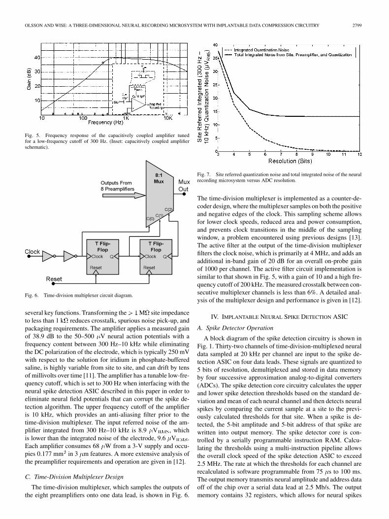
Fig. 5. Frequency response of the capacitively coupled amplifier tunedfor a low-frequency cutoff of 300 Hz. (Inset: capacitively coupled amplifierschematic).
Fig. 6. Time-division multiplexer circuit diagram.
several key functions. Transforming the M site impedanceto less than 1 k reduces crosstalk, spurious noise pick-up, andpackaging requirements. The amplifier applies a measured gainof 38.9 dB to the 50–500 V neural action potentials with afrequency content between 300 Hz–10 kHz while eliminatingthe DC polarization of the electrode, which is typically 250 mVwith respect to the solution for iridium in phosphate-bufferedsaline, is highly variable from site to site, and can drift by tensof millivolts over time [11]. The amplifier has a tunable low-fre-quency cutoff, which is set to 300 Hz when interfacing with theneural spike detection ASIC described in this paper in order toeliminate neural field potentials that can corrupt the spike de-tection algorithm. The upper frequency cutoff of the amplifieris 10 kHz, which provides an anti-aliasing filter prior to thetime-division multiplexer. The input referred noise of the am-plifier integrated from 300 Hz–10 kHz is 8.9 V , whichis lower than the integrated noise of the electrode, 9.6 V .Each amplifier consumes 68 W from a 3-V supply and occu-pies 0.177 mm in 3 m features. A more extensive analysis ofthe preamplifier requirements and operation are given in [12].
C. Time-Division Multiplexer Design
The time-division multiplexer, which samples the outputs ofthe eight preamplifiers onto one data lead, is shown in Fig. 6.
Fig. 7. Site referred quantization noise and total integrated noise of the neuralrecording microsystem versus ADC resolution.
The time-division multiplexer is implemented as a counter-de-coder design, where the multiplexer samples on both the positiveand negative edges of the clock. This sampling scheme allowsfor lower clock speeds, reduced area and power consumption,and prevents clock transitions in the middle of the samplingwindow, a problem encountered using previous designs [13].The active filter at the output of the time-division multiplexerfilters the clock noise, which is primarily at 4 MHz, and adds anadditional in-band gain of 20 dB for an overall on-probe gainof 1000 per channel. The active filter circuit implementation issimilar to that shown in Fig. 5, with a gain of 10 and a high fre-quency cutoff of 200 kHz. The measured crosstalk between con-secutive multiplexer channels is less than 6%. A detailed anal-ysis of the multiplexer design and performance is given in [12].
IV. IMPLANTABLE NEURAL SPIKE DETECTION ASIC
A. Spike Detector Operation
A block diagram of the spike detection circuitry is shown inFig. 1. Thirty-two channels of time-division-multiplexed neuraldata sampled at 20 kHz per channel are input to the spike de-tection ASIC on four data leads. These signals are quantized to5 bits of resolution, demultiplexed and stored in data memoryby four successive approximation analog-to-digital converters(ADCs). The spike detection core circuitry calculates the upperand lower spike detection thresholds based on the standard de-viation and mean of each neural channel and then detects neuralspikes by comparing the current sample at a site to the previ-ously calculated thresholds for that site. When a spike is de-tected, the 5-bit amplitude and 5-bit address of that spike arewritten into output memory. The spike detector core is con-trolled by a serially programmable instruction RAM. Calcu-lating the thresholds using a multi-instruction pipeline allowsthe overall clock speed of the spike detection ASIC to exceed2.5 MHz. The rate at which the thresholds for each channel arerecalculated is software programmable from 75 s to 100 ms.The output memory transmits neural amplitude and address dataoff of the chip over a serial data lead at 2.5 Mb/s. The outputmemory contains 32 registers, which allows for neural spikes

2800 IEEE JOURNAL OF SOLID-STATE CIRCUITS, VOL. 40, NO. 12, DECEMBER 2005
Fig. 8. Successive approximation ADC block diagram.
Fig. 9. Track and latch comparator schematic.
on 50 consecutive channels before a spike is missed. The outputmemory operates as a first-in/first-out (FIFO) queue with a la-tency period of 2.84 s added each time neural spikes are de-tected on consecutive scans. This yields a maximum latency (oc-curring only under very rare circumstances such as during anepileptic seizure) of 142 s that can be corrected in the externaldecoding software because the clock rate and channel samplingorder are known. The spike detector core circuitry and the suc-cessive approximation register used in the ADC were designedusing Verilog HDL along with synthesis and auto place androute tools while the memory and analog ADC electronics weredesigned using Spice and full custom layout. The synthesizedspike detector core circuitry consumes 2.5 mm , the on-chip in-struction, data, and output memory occupies 1.44 mm and theADCs consume 0.3 mm , for a total of 6 mm in AMI 0.5 mCMOS.
B. Neural Analog-to-Digital Converter Design
There is widespread disagreement over the requiredresolution needed to quantize neural action potentials.The integrated RMS quantization noise is given by [14]
(2)
Fig. 10. Timing diagram for the probe multiplexers and the four successiveapproximation A/D converters.
where is white noise distributed between andis the sampling frequency. For the design of the ADC in
this paper, several assumptions supported by measured datawere made: neural action potentials have a bandwidth between300 Hz and 10 kHz and a maximum amplitude of 500 V,

OLSSON AND WISE: A THREE-DIMENSIONAL NEURAL RECORDING MICROSYSTEM WITH IMPLANTABLE DATA COMPRESSION CIRCUITRY 2801
Fig. 11. Current source DAC schematic.
the total measured integrated noise (300 Hz–10 kHz) from arecording site is 9.6 V and from the on-probe circuitry is8.9 V and the on-probe gain before the ADC is 60 dB.The total integrated quantization noise referred to the siteand the total integrated quantization, amplifier, and site noiseversus ADC resolution are shown in Fig. 7. From this plot,5-bit quantization was chosen as the optimum resolution be-cause the input noise is dominated by the site/preamplifier forquantization of 5 bits and above and the power consumption,area, and clock speed of the ADC and DSP circuitry increaseswith increasing ADC resolution. In order to preserve this reso-lution, much of the spike detector DSP operates at 8–12 bits.Since there is a gain of 1000 in the neural recording mi-crosystem before the ADC, the LSB is 31.25 V referred to thesite, and the maximum spike amplitude that can be digitized is
500 V. This results in a total integrated quantization noise of8.9 V . Five-bit quantization increases the total integratednoise (300 Hz–10 kHz) in the system from 13.1 V to15.8 V .
A block diagram of the successive approximation ADC isshown in Fig. 8. The input sample and hold circuit, samples thetime-division multiplexed neural data 7/8 of the way throughthe sampling window, which reduces multiplexer crosstalk [12].A dummy switch has been added to reduce clock feed-throughin the sample and hold circuit [14]. The track and latch com-parator, Fig. 9, compares the sampled data to the referencevoltage provided by the digital-to-analog converter (DAC). Thecomparator features an input differential amplifier, transistors
– , with a small gain of 4 for high-speed operation. Theunity gain buffer at the comparator input prevents kickbackfrom the latch, formed by inverters and , frombeing stored on the sample-and-hold capacitor. In the latchphase, positive feedback allows very small voltage differencesat the input to be resolved very quickly at the output. During thetrack phase, the outputs of and are shorted to-gether to prevent hysteresis. In addition to controlling the DAC,
the synthesized SAR controller (shown as the A/D and probetiming controller block in Fig. 2) also provides the multiplexerclock to the neural probes, probe clock, the sampling clock tothe A/D, hold, the latch signal to the comparators, and controlsthe writing of data from the ADCs into the data memory, writedata(0:3). A timing diagram illustrating the communicationbetween the ADCs, data memory and on-probe time-divisionmultiplexers is shown in Fig. 10.
A diagram of the current source DAC is shown in Fig. 11. Thecurrent sources (M8–M22) are turned on or off depending on thevalue of the digital feedback bits, – . While this architectureis often used to achieve high-speed DACs by steering currentsbetween ground and the negative terminal of a transimpedanceamplifier [14], here the current sources are turned off insteadof switched to ground when they are not in use. While this de-creases the speed of the design due to transistor “wake up,” theaverage power consumption of the DAC is reduced by almost58%. The nominal value of is 25 A, which allows quanti-zation of 500 V action potentials with an LSB of 31.25 V.
is adjustable for recording spikes which have a wider/smallersignal swing with a subsequent increase/decrease in the leastsignificant bit. Both pMOS and nMOS current sources havebeen used here to allow the analog output of the DAC to achieveboth positive and negative values. The linearity of the DAC de-pends on how well the currents can be matched between thenMOS and pMOS devices. This puts stringent restrictions onthe maximum tolerable current mirror error. In this design, a6% current mirror error between the nMOS and pMOS currentsources would cause a 1-bit DNL at the output of the DAC.To provide low current mirror error at a 3-V supply, the wideswing current mirror architecture [14] consisting of transistors
– was chosen. The transimpedance amplifier is shown inFig. 12. The amplifier features a wide-swing output stage [15],which is necessary because standard output stages cannot obtainthe desired output swing from a 3-V supply.

2802 IEEE JOURNAL OF SOLID-STATE CIRCUITS, VOL. 40, NO. 12, DECEMBER 2005
Fig. 12. Wide-swing transimpedance amplifier.
Fig. 13. ADC transfer characteristic.
V. MEASURED RESULTS
A. Analog-to-Digital Converter
The spike detection ASIC has been fabricated and is picturedin Fig. 1. The measured transfer characteristic of the ADC isshown in Fig. 13 where the offset and gain errors here havebeen trimmed via and in Fig. 11. The maximum DNLis 0.3 LSB while the maximum INL is 0.5 LSB and thereare no missing codes. The power consumption of each ADCis 600 W, including the bias circuitry, operating at a clockfrequency of 2.5 MHz.
B. System Level Spike Detector Testing
In order to evaluate the performance of the spike detectionASIC, neural waveforms recorded using multiplexed activeprobes were reconstructed using Lab View and a DAQ cardand were input to the spike detector. The response of the spikedetector to a sample neural waveform with the thresholds setto three times the standard deviation above/below the meanis shown in Fig. 14. The average bandwidth savings acrossfive sample waveforms is 92% with a maximum bandwidthsavings of 95%. On average, 86% of the transmitted data is
Fig. 14. Response of the spike detection ASIC to a neural waveform recordedusing active microprobes. The top trace is the reconstructed neural signal inputto the spike detector. The middle trace is the serial digital output of the spikedetector. The bottom trace is the output waveform reconstructed from the serialdigital output data.
associated with neural spikes and no spikes have been missed.The predicted bandwidth savings based on these records whenrecording from neurons in motor cortex with a firing rate of50 firings/s [9] is 91%. Overall microsystem performance issummarized in Table I.
C. Neural Spike Discrimination
The ability to discriminate between neural spikes on a singlechannel improves the control of neuroprosthetics and aids inneuroscience experiments. Vibert [16] evaluated neural spikeseparation based on eight parameters of the neural spike andconcluded that using three parameters, (the maximumpositive spike amplitude), (the minimum negative spikeamplitude), and (the time between and ), notonly adequately sorted spikes but was actually superior tospike separation using more parameters. This was because theadditional parameters were all correlated with one or moreof , , and , while , , and werefound to be uncorrelated. Separation of neurons using these

OLSSON AND WISE: A THREE-DIMENSIONAL NEURAL RECORDING MICROSYSTEM WITH IMPLANTABLE DATA COMPRESSION CIRCUITRY 2803
TABLE IMICROSYSTEM PERFORMANCE
three parameters is based on physiology where andfor a particular neuron are dependent on the distance of
the site from the neuron, the size of the neuron, and the spatialconfiguration of the dendritic tree [17]. The first principalcomponent, represented by amplitude parameters and
, contained 60%–65% [16] of the total information inVibert’s study. The time between and is alsoderived from physiology and is dependent on the distance of therecording site from the neuron axon hillock [18]. This secondprincipal component contained 15%–20% [16] of the informa-tion in Vibert’s experiments. Since the neural spike detectionASIC shown in Fig. 1 preserves the maximum neural spikeamplitude , the minimum neural spike amplitude ,and the time , between and , it is possible todiscriminate between different neurons detected on the samechannel.
VI. CONCLUSION
A 256-site neural recording microsystem with implantabledata compression circuitry has been developed. Four active
neural probes with integrated circuitry for site selection, ampli-fication, and multiplexing drive an embedded data-compressionASIC that successfully detects neural spikes in the presenceof neural and circuit noise. The spike detector quantizes anddemultiplexes the neural data, calculates upper and lower spikethresholds based on the mean and standard deviation of eachchannel, detects neural spikes in the presence of noise, andserially shifts the address and amplitude of detected spikesoff-chip on one data lead. The average bandwidth savingswhen the thresholds are set to three standard deviations aboveand below the mean is 92%, indicating that 12.5 times asmany neural channels can be recorded simultaneously across afinite bandwidth wireless link. Given a telemetry bandwidth of2.5 Mb/s [6], this increases the total number of channels thatcan be transmitted transcutaneously at 5 bits of resolution anda sampling rate of 20 kHz/channel from 25 to 312.
ACKNOWLEDGMENT
The authors wish to thank Dr. W. Heetderks of the NeuralProsthesis Program, National Institutes of Neurological Dis-orders and Stroke, for his encouragement and support of this

2804 IEEE JOURNAL OF SOLID-STATE CIRCUITS, VOL. 40, NO. 12, DECEMBER 2005
work. The assistance of N. Gulari, G. Eadara, Dr. B. Jamieson,Dr. A. DeHennis, B. Casey, R. Gordenker, and J. Hetke is alsovery much appreciated.
REFERENCES
[1] A. P. Georgopoulos and J. Ashe et al., “The motor cortex and the codingof force,” Science, vol. 256, no. 5064, pp. 1692–1695, 1992.
[2] D. M. Taylor, S. I. H. Tillery, and A. B. Schwartz, “Direct cortical con-trol of 3-D neuroprosthetic devices,” Science, vol. 296, no. 5574, pp.1829–1832, 2002.
[3] M. D. Serruya, N. G. Hatsopoulos, L. Paninski, M. R. Fellows, and J. P.Donoghue, “Instant neural control of a movement signal,” Nature, vol.416, no. 6877, pp. 141–142, 2002.
[4] J. M. Carmena, M. A. Lebedev, R. E. Crist, J. E. O’Doherty, D. M. San-tucci, D. F. Dimitrov, P. G. Patil, C. S. Henriquez, and M. A. L. Nicolelis,“Learning to control a brain-machine interface for reaching and graspingby primates,” PLoS Biology, vol. 1, no. 2, pp. 1–16, 2003.
[5] J. Csicsvari, D. A. Henze, B. Jamieson, K. D. Harris, A. Sirota, P. Bartho,K. D. Wise, and G. Buzsaki, “Massively parallel recording of unit andlocal field potentials with silicon based electrodes,” J. Neurophys., vol.90, no. 2, pp. 1323–1341, 2003.
[6] H. Yu, R. H. Olsson III, K. D. Wise, and K. Najafi, “A wirelessmicrosystem for multichannel neural recording microprobes,” in Proc.Solid-State Sensor, Actuator, and Microsystems Workshop, Jun. 2004,pp. 107–110.
[7] R. H. Olsson III, M. N. Gulari, and K. D. Wise, “Silicon neural recordingarrays with on-chip signal processing for in vivo data acquisition,” inProc. IEEE/EMBS Special Topic Conf. Microtechnologies in Medicineand Biology, Madison, WI, 2002, pp. 237–240.
[8] Q. Bai, K. D. Wise, and R. J. Anderson, “A high-yield micro-assemblystructure for three-dimensional electrode arrays,” IEEE Trans. Biomed.Eng., vol. 47, no. 3, pp. 281–289, Mar. 2000.
[9] I. Obeid and P. D. Wolf, “Evaluation of spike-detection algorithms fora brain machine interface application,” IEEE Trans. Biomed. Eng., vol.51, no. 6, pp. 905–911, Jun. 2004.
[10] R. R. Harrison, “A low-power integrated circuit for adaptive detectionof action potentials in noisy signals,” in Proc. 25th Annu. Meeting En-gineering in Medicine and Biology Society, 2003, pp. 3325–3328.
[11] Q. Bai and K. D. Wise, “Single-unit neural recordings with active micro-electrode arrays,” IEEE Trans. Biomed. Eng., vol. 48, no. 8, pp. 911–920,Aug. 2001.
[12] R. H. Olsson III, D. L. Buhl, A. M. Sirota, G. Buzsaki, and K. D. Wise,“Band-tunable and multiplexed integrated circuits for simultaneousrecording and stimulation with microelectrode arrays,” IEEE Trans.Biomed. Eng., vol. 52, no. 7, pp. 1303–1311, Jul. 2005.
[13] J. L. Lund, “Performance characteristics of active silicon microelec-trode arrays,” Ph.D. dissertation, Dept. Electr. Eng. Comput. Sci., Univ.Michigan, Ann Arbor, 1996.
[14] D. A. Johns and K. Martin, Analog Integrated Circuit Design. NewYork: Wiley, 1997.
[15] F. You, S. H. K. Embabi, and E. Sanchez-Sinencio, “1.5 V class ABoutput buffer,” in Int. Symp. Low Power Electronics and Design Dig.Tech. Papers, Monterey, CA, 1996, pp. 285–288.
[16] J. F. Vibert and J. Costa, “Spike separation in multiunit records: A multi-variate analysis of spike descriptive parameters,” Electroencephal. Clin.Neurophys., vol. 47, no. 1, pp. 172–182, 1979.
[17] W. Rall, “Electrophysiology of a dendritic neuron model,” J. Biophys.,vol. 2, no. 1, pp. 145–167, 1962.
[18] F. Rosenthal, J. W. Woodbury, and H. D. Patton, “Dipole characteristicsof pyramidal cell activity in cat postcruciate cortex,” J. Neurophys., vol.29, no. 1, pp. 612–625, 1966.
Roy H. Olsson III (S’99–M’05) was born in Nevada,MO, in 1976. He received B.S. degrees (Summa CumLaude) in electrical engineering and in computer en-gineering from West Virginia University in 1999 andthe MS and Ph.D. degrees in electrical engineeringfrom the University of Michigan, Ann Arbor in 2001and 2004.
After completing his B.S. Degrees, he internedat Lucent Technologies, where he designed mixedsignal electronics for cellular phone applications.From 1999 to 2004 he was a Research Assistant in
the Center for Wireless Integrated MicroSystems (WIMS) at the University ofMichigan, where his doctoral research was in the development of implantableelectronics for neural recording applications including amplification, multi-plexing, and data compression circuitry. In July 2004, he joined the MEMSDevice Technologies Group at Sandia National Laboratories, Albuquerque, NMas a Senior Member of Technical Staff. His current research areas include RFmicroresonators, RF transceivers, neural prosthetics, bio-interface electronicsand low noise readout circuits for optical MEMS sensors.
Dr. Olsson won 1st prize in the conceptual category and best overall paper atthe 2002 Design Automation Conference student design contest. He is a memberof Etta Kappa Nu, Tau Beta Pi, the IEEE Solid State Circuits Society and Engi-neering in Medicine and Biology Society.
Kensall D. Wise (S’61–M’69–SM’83–F’86) re-ceived the B.S.E.E. degree with highest distinctionfrom Purdue University, West Lafayette, IN, in1963 and the M.S. and Ph.D. degrees in electricalengineering from Stanford University, Stanford, CA,in 1964 and 1969, respectively.
From 1963 to 1965 (on leave 1965–1969) and from1972 to 1974, he was a Member of Technical Staffat Bell Telephone Laboratories, where his work wasconcerned with the exploratory development of inte-grated electronics for use in telephone communica-
tions. From 1965 to 1972, he was a Research Assistant and then a ResearchAssociate and Lecturer in the Department of Electrical Engineering at StanfordUniversity, working on the development of integrated circuit technology and itsapplication to solid-state sensors. In 1974, he joined the Department of Elec-trical Engineering and Computer Science at the University of Michigan, AnnArbor, where he is now the J. Reid and Polly Anderson Professor of Manufac-turing Technology and Director of the NSF Engineering Research Center forWireless Integrated MicroSystems. His present research interests focus on thedevelopment of integrated microsystems for health care, process control, andenvironmental monitoring.
Dr. Wise organized and served as the first chairman of the Technical Sub-committee on Solid-State Sensors of the IEEE Electron Devices Society (EDS).He was General Chairman of the 1984 IEEE Solid-State Sensor Conference,Technical Program Chairman of the IEEE International Conference on Solid-State Sensors and Actuators (1985), and IEEE EDS National Lecturer (1986).He served as General Chairman of the 1997 IEEE International Conferenceon Solid-State Sensors and Actuators. Dr. Wise received the Paul RappaportAward from the EDS (1990), a Distinguished Faculty Achievement Award fromthe University of Michigan (1995), the Columbus Prize from the ChristopherColumbus Fellowship Foundation (1996), the SRC Aristotle Award (1997), andthe 1999 IEEE Solid-State Circuits Field Award. In 2002 he was named theWilliam Gould Dow Distinguished University Professor at the University ofMichigan. He is a Fellow of the AIMBE, and a member of the U.S. NationalAcademy of Engineering.