A Systematic Electromagnetic-Circuit Method for EMI … · · 2016-06-04(EMC) has become a major...
14
Title A Systematic Electromagnetic-Circuit Method for EMI Analysis of Coupled Interconnects on Dispersive Dielectrics Author(s) Tang, M; Lu, J.Q.; Mao, J.F.; Jiang, L Citation IEEE Transactions on Microwave Theory and Techniques, 2013, v. 61, p. 1-13 Issued Date 2013 URL http://hdl.handle.net/10722/185863 Rights Creative Commons: Attribution 3.0 Hong Kong License
Transcript of A Systematic Electromagnetic-Circuit Method for EMI … · · 2016-06-04(EMC) has become a major...

Title A Systematic Electromagnetic-Circuit Method for EMI Analysisof Coupled Interconnects on Dispersive Dielectrics
Author(s) Tang, M; Lu, J.Q.; Mao, J.F.; Jiang, L
Citation IEEE Transactions on Microwave Theory and Techniques, 2013,v. 61, p. 1-13
Issued Date 2013
URL http://hdl.handle.net/10722/185863
Rights Creative Commons: Attribution 3.0 Hong Kong License

IEEE TRANSACTIONS ON MICROWAVE THEORY AND TECHNIQUES, VOL. 61, NO. 1, JANUARY 2013 1
A Systematic Electromagnetic-Circuit Methodfor EMI Analysis of Coupled Interconnects
on Dispersive DielectricsMin Tang, Member, IEEE, Jiaqing Lu, Junfa Mao, Fellow, IEEE, and Lijun Jiang, Member, IEEE
Abstract—This paper presents a systematic electromagnetic-cir-cuit method for efficient simulation of coupled interconnects ondispersive dielectrics in the presence of electromagnetic interfer-ence. The dispersive substrate of coupled interconnects is charac-terized by the multiterm Debye or Lorentz formula. According tothe differential equations derived from the equivalent circuit mod-eling of dispersive media, the full-wave finite-difference time-do-main algorithm is utilized to capture accurate field in a dispersivesubstrate. The effects of incident field, under the quasi-TEM as-sumption, are then represented by the distributed sources alongtransmission lines. An efficient algorithm based on the waveformrelaxation with transverse partitioning (WR-TP) is employed forfast simulation of coupled transmission lines. A simple and clearderivation of the relaxation sources inWR-TP is described and thecompact results are given. The impact of dispersive dielectrics onthe incident field, and thus to the transient response of intercon-nects, is investigated by comparison with conventional techniques.Several numerical examples are given to illustrate the accuracyand efficiency of the proposed method.
Index Terms—Electromagnetic interference (EMI), finite differ-ence time domain (FDTD), frequency-dependent parameters, in-terconnects, waveform relaxation.
I. INTRODUCTION
W ITH THE ever-increasing operating speeds and de-creasing structure sizes, electromagnetic compatibility
(EMC) has become a major concern in modern circuit designssince high-speed interconnects at various hierarchical levelsmay serve as spurious antennas at high frequencies and leadto strong coupling of electromagnetic interference (EMI). Thiselectromagnetic coupling can seriously deteriorate the signalintegrity of the design and cause false switching of waveforms.Meanwhile, due to skin, edge, and proximity effects and lossysubstrates, the frequency dependence of interconnect param-eters becomes more and more popular in practical cases [1].Successful modeling of interconnects requires accurate material
Manuscript received May 16, 2012; accepted August 28, 2012. Date of pub-lication October 18, 2012; date of current version January 17, 2013. This workwas supported in part by the National Science Foundation of China under Grant60906016 and in part by the National Basic Research Program of China underGrant 2009CB320202.M. Tang, J. Lu, and J. Mao are with the Key Laboratory of Ministry of Ed-
ucation of China for Research of Design and Electromagnetic Compatibilityof High Speed Electronic Systems, Shanghai Jiao Tong University, Shanghai200240, China (e-mail: [email protected]; [email protected]).L. Jiang is with the Department of Electrical and Electronic Engineering, Uni-
versity of Hong Kong, Kowloon, Hong Kong (e-mail: [email protected]).Color versions of one or more of the figures in this paper are available online
at http://ieeexplore.ieee.org.Digital Object Identifier 10.1109/TMTT.2012.2220562
parameter characterization over a wide band of frequencies.For example, wideband frequency-domain characterization ofFR-4 has been described in [2] and [3], where the real andimaginary parts of the complex permittivity were related by theHilbert transform, a causal response in the time domain wasobtained thereby. In [4], the partial-element equivalent-circuit(PEEC) modeling of dispersive dielectrics was introduced,where the general media are represented by the Debye, as wellas Lorentz, models and its validity was illustrated by differenttransmission-line structures.Incorporating the effects of incident electromagnetic fields
into interconnect simulation has been a problem of interest formany years. The most general approach to solve this problemis the full-wave technique formulated as the 3-D electromag-netic field. While accurate, this kind of algorithm would re-quire great computational resources if applied to practical sizedprinted circuit board (PCB) problems. Thus, for many prac-tical cases, it is more common to use the distributed transmis-sion-line model under the quasi-TEM assumption, where the ex-istence of external field coupling is introduced by distributedvoltage and current sources along the lines [5], [6]. Varioustechniques have been proposed for solving the transmission-linemodel with distributed sources [5]–[15]. To guarantee the pas-sivity in the developed model, an algorithm based on the ma-trix rational approximation (MRA) [16] has been presented formacromodeling of transmission lines. By employing the delayextraction technique, this method can also deal with long delaytransmission lines in the presence of EMI [13]. Recently, a newspectral formulation has also been presented for the transientanalysis of plane-wave coupling to transmission lines with fre-quency-dependent parameters [15]. Nevertheless, most of thesetechniques treat the medium surrounding interconnects as ho-mogenous air in the calculation of incident field. Despite its sim-plicity, imposing such a condition may produce poor results athigh frequencies. In [11], an efficient physical optics techniquehas been utilized to calculated the field in a layered inhomoge-neous medium. In [12], a full-wave field simulation has beencarried out to accurately characterize the perturbation of the in-cident field due to the dielectric substrate. The dispersion of sub-strate material, however, was not taken into consideration.For EMI analysis, another challenge is that of the large
number of coupled lines in an interconnection structure. Inrecent years, an efficient method based on waveform relaxationwith transverse partitioning (WR-TP) [17] was presented forthe simulation of large coupled interconnects. In WR-TP, thecoupling effects due to the neighboring lines are represented by
0018-9480/$31.00 © 2012 IEEE

2 IEEE TRANSACTIONS ON MICROWAVE THEORY AND TECHNIQUES, VOL. 61, NO. 1, JANUARY 2013
the relaxation voltage and current sources within the sub-cir-cuits. The computational cost of this algorithm grows almostlinearly with the number of coupled lines, providing a signifi-cant speedup compared to conventional model. It is also highlysuitable for parallel implementation for further improvementof efficiency. In the past few years, this WR-TP techniquehas been extended to the simulation of coupled interconnectswith frequency-dependent parameters [18]. More recently,a parallel algorithm based on the physical and time-domainpartitioning has been proposed for simulations of massivelycoupled interconnects [19]. The WR-TP algorithm has alsobeen implemented for fast simulation of interconnects in thepresence of incident field [14]. Nevertheless, the impact ofthe dielectric substrate on the incident field was ignored in thecalculation, which would cause incorrect transient responsealong the transmission lines.In this paper, an efficient hybrid method for EMI analysis
of coupled interconnects on dispersive dielectrics is presented.The implementation of this method consists of two stages, oneis for electromagnetic simulation and the other is for circuitsimulation. In the electromagnetic simulation, in order to ac-curately model the field in a dispersive substrate, a full-wavefinite-difference time-domain (FDTD) algorithm is exploitedbased on the differential equations derived from the equivalentcircuit modeling (ECM) technique. Both the Debye and Lorentzmedia are taken into consideration in the modeling. In the re-gion of circuit simulation, the WR-TP approach is utilized forefficient computation of coupled transmission lines with fre-quency-dependent parameters in the presence of EMI. The re-laxation voltage and current sources in the algorithm are de-rived and described in a compact form. Additional distributedvoltage sources, which denote the effects of the excitation field,are computed with the results obtained from the electromagneticsimulation.This paper is organized as follows. In Section II, the mod-
eling of transmission lines with frequency-dependent parame-ters and incident field coupling is described. In Section III, theWR-TP algorithm is employed for efficient EMI simulation ofcoupled interconnects. In Section IV, full-wave electromagneticsimulation of the incident field in the dispersive media is pro-posed. The numerical results and conclusion are presented inSections V and VI, respectively
II. MODELING OF INTERCONNECTS WITHFREQUENCY-DEPENDENT PARAMETERS AND INCIDENT
FIELD COUPLING
A. Formulation of Transmission Lines for EMI Analysis
Consider -coupled transmission lines excited by an incidentelectromagnetic field, as shown in Fig. 1.Depending on the definition of line voltage, two different, but
equivalent formulations can be derived to describe transmissionlines [6]. The transmission-line equations in terms of total volt-ages are given by
(1a)
Fig. 1. Geometry of interconnects with incident field coupling (the substrate isnot depicted for clarity).
(1b)
where
...
...
(1c)
...
...
(1d)
In , is expressed as
...
...
(1e)
where is the axial component of the incident field, is thetransverse component of the incident field, denotes theth conductor, and is a contour in the transverse plane.From (1a)–(1e), it is easy to derive the transmission-line
equations in terms of scattered voltages as
(2a)
(2b)
The scattered voltage along the transmission lines is relatedto the total voltage by the following expression [6]:
(3a)
where
...
...
(3b)

TANG et al.: SYSTEMATIC ELECTROMAGNETIC-CIRCUIT METHOD FOR EMI ANALYSIS 3
By comparison, the transmission-line equations in terms ofscattered voltages are more convenient to deal with lines withfrequency-dependent parameters since there is not distributedcurrent source in (2b). Therefore, the following derivations areall based on the expressions of (2a) and (2b). For convenience,however, the superscript on the scattered voltage will besuppressed.
B. Modeling of Transmission Lines WithFrequency-Dependent Parameters
Without loss of generality, it is assumed that the per-unit-length (p.u.l.) frequency-dependent parameters of transmissionlines are obtained at a set of discrete frequencies. The vector-fit-ting algorithm [20] followed by a passive check and compensa-tion technique [21] is used to generate the positive-real closedform of the series impedance matrix and parallel admittance ma-trix
(4a)
(4b)
where and represent the number of poles used in therational approximation. These equations can be cast into the re-alizable form of an equivalent circuit network as [22]
(5a)
(5b)
where and are the equivalent resistance, and arethe equivalent conductance, and are given by
(5c)
(5d)
(5e)
(5f)
The generalized equivalent circuit representations [23] of seriesimpedance matrix and parallel admittance matrix aredescribed in Fig. 2. The equivalent inductance and equiva-lent capacitance in Fig. 2 are given, respectively, by
(6a)
and
(6b)
Fig. 2. Generalized equivalent circuits. (a) Representation of series impedance.(b) Representation of parallel admittance.
From Fig. 2, it is straightforward to obtain
(7a)
(7b)
Combining (6a) and (6b) and (7a) and (7b), we have the rela-tionships
(8a)
(8b)
where . Despite their simplicity, these relation-ships are important for the derivation of relaxation sources inthe WR-TP algorithm presented in Section III. They imply thatthe coupling effects of off-diagonal elements in and areessentially equivalent. Analogously, the coupling effects of theoff-diagonal elements in and are also equivalent.
III. IMPLEMENTATION OF WAVEFORM RELAXATIONWITH TRANSVERSE PARTITIONING
A. Formulation of WR-TP for EMI Simulation
In the implementation of the WR-TP technique, the expres-sions of coupled transmission lines (2a) and (2b) should bewritten in the form of individual lines with relaxation sources.The resulting equations in a matrix form is given by
(9a)
where
(9b)
(9c)
(9d)
(9e)
Here, the functions and are used to obtain thediagonal and nondiagonal entries of a matrix, respectively.
4 IEEE TRANSACTIONS ON MICROWAVE THEORY AND TECHNIQUES, VOL. 61, NO. 1, JANUARY 2013
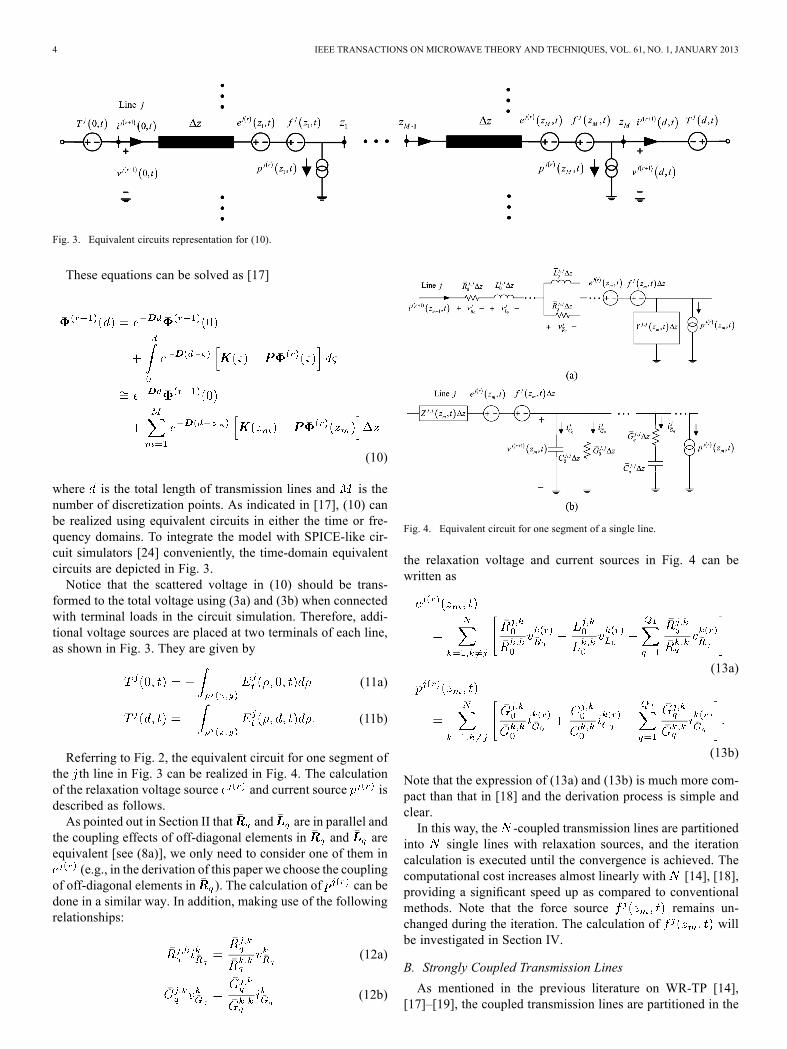
Fig. 3. Equivalent circuits representation for (10).
These equations can be solved as [17]
(10)
where is the total length of transmission lines and is thenumber of discretization points. As indicated in [17], (10) canbe realized using equivalent circuits in either the time or fre-quency domains. To integrate the model with SPICE-like cir-cuit simulators [24] conveniently, the time-domain equivalentcircuits are depicted in Fig. 3.Notice that the scattered voltage in (10) should be trans-
formed to the total voltage using (3a) and (3b) when connectedwith terminal loads in the circuit simulation. Therefore, addi-tional voltage sources are placed at two terminals of each line,as shown in Fig. 3. They are given by
(11a)
(11b)
Referring to Fig. 2, the equivalent circuit for one segment ofthe th line in Fig. 3 can be realized in Fig. 4. The calculationof the relaxation voltage source and current source isdescribed as follows.As pointed out in Section II that and are in parallel and
the coupling effects of off-diagonal elements in and areequivalent [see (8a)], we only need to consider one of them in
(e.g., in the derivation of this paper we choose the couplingof off-diagonal elements in ). The calculation of can bedone in a similar way. In addition, making use of the followingrelationships:
(12a)
(12b)
Fig. 4. Equivalent circuit for one segment of a single line.
the relaxation voltage and current sources in Fig. 4 can bewritten as
(13a)
(13b)
Note that the expression of (13a) and (13b) is much more com-pact than that in [18] and the derivation process is simple andclear.In this way, the -coupled transmission lines are partitioned
into single lines with relaxation sources, and the iterationcalculation is executed until the convergence is achieved. Thecomputational cost increases almost linearly with [14], [18],providing a significant speed up as compared to conventionalmethods. Note that the force source remains un-changed during the iteration. The calculation of willbe investigated in Section IV.
B. Strongly Coupled Transmission Lines
As mentioned in the previous literature on WR-TP [14],[17]–[19], the coupled transmission lines are partitioned in the

TANG et al.: SYSTEMATIC ELECTROMAGNETIC-CIRCUIT METHOD FOR EMI ANALYSIS 5
transverse direction taking advantage of the relatively weakcoupling between individual traces. If several traces are placedclose together, strong coupling between them will exist. In thiscase, they should be grouped together within the same sub-cir-cuit [17]. This idea can be implemented in a straightforwardway by making some modifications to the relaxation sourcesderived earlier in this section.For simplicity and without loss of generality, it is assumed
that strong coupling exists between the lines and . Again,we consider themodeling of the th line for example. The equiv-alent circuits described in Figs. 3 and 4 are still available, exceptthat the relaxation voltage and current sources are required to bemodified. They can be divided into two parts, one is for strongcoupling from lines and , and the other is for the relativelyweak coupling from other lines. The former is the controlledsource of the th iteration, while the latter is that of theth iteration that is known. They can be described by
(14a)
(14b)
where
(14c)
(14d)
(14e)
(14f)
The similar treatment can made for lines and , while otherlines remain the expressions of (13a) and (13b).It is worth noting that the term of “strong coupling” men-
tioned above is actually a relative concept.Whether several linesare suggested to be grouped together in a sub-circuit is not deter-mined by the absolute values of coupling coefficients, but theirrelative values comparing with other lines.
IV. MODELING AND SIMULATION OF DISPERSIVE MEDIA
In this paper, it is assumed that the coupled interconnects areplaced on or embedded in a dispersive substrate. In order toobtain the distribution voltage sources in (2a) produced by theexternal field coupling, the corresponding field quantities are
calculated with the full-wave electromagnetic simulation in theabsence of the conductors [12]. For accurate modeling, it is im-portant to consider frequency variations of the dielectric param-eters, which are available as table data provided by the manufac-turers or described by standard physics-based formulations likethe Debye or Lorentz models [2]–[4]. In practice, the multitermDebye function expansion is suitable for modeling the dielectricbehavior of most PCB materials (e.g., FR-4 in [2]).Over the past two decades, approaches based on the Yee
FDTD algorithm have been widely studied and developed formodeling dispersive materials [25]. In general, these methodscan be divided into three basic categories: recursive convolu-tion methods [26], [27], -transform methods [28] and auxiliarydifferential equation (ADE) methods [29]–[32]. Recently, anequivalent-circuit FDTD method [33] has been proposed forthe modeling of dispersive materials. A complete circuitalformulation of the conventional FDTD was represented in thismethod. In [4], the similar equivalent-circuit representationwas also exploited in the development of a PEEC formulationfor dispersive media. In this section, however, our purpose is tocalculate the fields in a dispersive substrate, the formulationsbased on the Maxwell equations are therefore more suitable.
A. ECM of Debye Media
For a Debye medium having poles, the expression of per-mittivity is written as
(15)
where is the permittivity of free space, is the permittivityat “infinite” frequency, is the variation inrelative permittivity due to the th pole, and is the th relax-ation time.Without loss of generality, theMaxwell curl equationconcerning the -directed electric field is given by
(16)
In contrast to the traditional methods with the introduction of theelectric polarization vector to develop ADEs [29], [31], a con-venient technique based on the ECM is utilized here (the equiv-alence between the ECM and ADE formulations is explained inthe Appendix). Inspired by the equivalent-circuit model of fre-quency-dependent interconnects in Section II, (16) can be rep-resented by an admittance-type ECM, as shown in Fig. 5, where
, , , , ,and .Based on Kirchhoff’s laws, it is straightforward to obtain the
following differential equations in the time domain:
(17a)
and
(17b)
where is the auxiliary variable.

6 IEEE TRANSACTIONS ON MICROWAVE THEORY AND TECHNIQUES, VOL. 61, NO. 1, JANUARY 2013
The FDTD algorithm is utilized to solve these coupled equa-tions. The resulting update formula for is given by
(18a)
and the corresponding update equation for the auxiliary variableis written by
(18b)
where
(18c)
(18d)
(18e)
(18f)
(18g)
The similar update equations can be derived for and com-ponents. On the other side, the update equations for are thesame to the standard FDTD schemes, e.g.,
(19)
Obtaining the electric field values from the full-wave simu-lation, the distributed force sources in (2a), as well as those in(3a), can be determined straightforwardly.
Fig. 5. Equivalent-circuit representation of multiterm Debye medium.
The accuracy of the algorithm can be evaluated by the nu-merical dispersion errors. Following the procedure in [34], thenumerical permittivity can be derived as given by
(20a)
where
(20b)
(20c)
Combining the expressions of lumped elements in Fig. 5, thenumerical permittivity can be rewritten as
(21)
which is the same to the result of an ADE-based algorithm de-noted as “D-DIM2” in [35]. Note that as becomes infinites-imal, (21) will reduce to the exact expression of (15). The rateof convergence is second order.Therefore, we can conclude that the numerical dispersion er-
rors as well as stability of the ECM approach are the same asthose of the ADE-based counterpart. Thus, they are not repeatedhere. The reader may refer to many excellent papers for detailedinformation [34]–[37].
B. ECM of Lorentz Media
As an extension, this ECM technique is readily exploited formodeling the Lorentz media as follows. For a Lorentz mediumwith poles, the expression of permittivity is given by
(22)
where is the th resonate frequency and is the th dampingcoefficient. The corresponding ECM is shown in Fig. 6, where
, , , ,, , , and .Likewise, a set of differential equations derived from Kirch-
hoff’s laws are given by
(23a)

TANG et al.: SYSTEMATIC ELECTROMAGNETIC-CIRCUIT METHOD FOR EMI ANALYSIS 7
Fig. 6. Equivalent-circuit representation of multiterm Lorentz medium.
(23b)
(23c)
where and are both auxiliary variables. Similar tothe case of the Debyemedium, the FDTD algorithm is employedto solve these coupled equations. Due to space limitations, it isnot presented here.
V. NUMERICAL RESULTS
In this section, four case studies are presented. The impactof dispersive dielectrics on the transient response of intercon-nects is illustrated in the first example. The capability of pro-posed method for the simulation of strongly coupled intercon-nects with nonlinear terminations is demonstrated in the secondexample. Incident field coupling to PCB traces with realistic fea-tures such as bends and vias are analyzed in the third example.The EMI simulation of the PCB placed in a metallic rectan-gular enclosure with multiple slots is given in the last example.For simplicity, a two-term Debye formulation is used to charac-terize the dispersive dielectric with , ,
, ns, and ns in all exam-ples, and the p.u.l. frequency-dependent parameters of coupledinterconnects are extracted using an electromagnetic simulator[38]. All the examples are executed using a PC with PentiumDual Core CPU (2.27 GHz).
A. Microstrip Lines With Plane-Wave Excitation
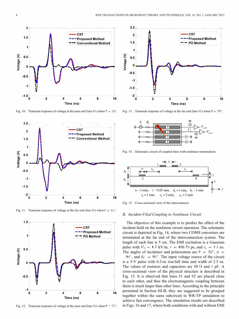
In this example, the proposed method is compared with twoexisting techniques. One is the conventional technique wherethe medium surrounding the interconnects is treated as homoge-nous air in the calculation of incident field. It is referred to as the“conventional model” for convenience. The other is the physicaloptics approach, which is based on the assumption that the sizeof a layered medium is infinitely large. It is referred to hereafteras “PO” for short.The test structure is the coupled microstrip lines on a disper-
sive substrate, and is exposed to an incident plane wave. Theplane wave is a Gaussian pulsewith kV/m, ps, and ns. The an-gles of incidence and polarization with respect to a sphericalcoordinate system are illustrated in Fig. 7, which are chosento be , , and in this example.The horizontal dimensions of the substrate is 30 cm 10 cm.The cross-sectional geometry of the interconnects and corre-sponding schematic circuit are depicted in Figs. 8 and 9, respec-tively.
Fig. 7. Illustration of the definition of incident field as a uniform plane wave.
Fig. 8. Cross-sectional view of the microstrip structure.
Fig. 9. Schematic circuit of the coupled lines.
Each line is terminated with a 50- resistor and a 1-pF capac-itor at the near and far ends. The length of the line is 20 cm. Incontrast to the conventional model, the proposed method em-ploys full-wave simulation to accurately model the field in adispersive substrate. The convolutional perfect matched layer(CPML) [25] absorbing boundary is employed to truncate thecomputational domain. After that, transmission-line equationswith distributed sources are solved using the WR-TP technique.The simulation results of transient voltages at the near and farends of line #1 are depicted in Figs. 10 and 11. To validate theaccuracy of the proposed method, the reference values are pro-vided by a 3-D electromagnetic simulator Computer SimulationTechnology (CST) [39]. As shown in the figures, the simulationresults of the proposed method are in very good agreement withthose of CST. In contrast, poor results from the conventionalmodel are observed, especially at the far end of the line. Notethat a similar phenomenon was also observed in [12], wherethe incident field coupling to interconnects with nondispersivedielectrics was studied, and the explanations were provided aswell.We then investigate the accuracy of PO method in simulating
the same structure. The implementation of the PO method [11]also involves two stages, one is the electromagnetic calculationbased on the PO principle and the other is the circuit simulation.Since the PO approach is based on the assumption that a layeredmedium extends to infinity in the lateral dimensions, its accu-racy will suffer when the finite substrate is simulated, especiallywith large incidence angles. To illustrate this phenomenon, thetransient responses at two ends of the interconnects with the in-cidence angle are depicted in Figs. 12 and 13. The di-vergence of the PO results is obvious. In contrast, the results ofthe proposed method agree quite well with the CST references.
8 IEEE TRANSACTIONS ON MICROWAVE THEORY AND TECHNIQUES, VOL. 61, NO. 1, JANUARY 2013
Fig. 10. Transient response of voltage at the near end (line #1) when .
Fig. 11. Transient response of voltage at the far end (line #1) when .
Fig. 12. Transient response of voltage at the near end (line #1) when .
Fig. 13. Transient response of voltage at the far end (line #1) when .
Fig. 14. Schematic circuit of coupled lines with nonlinear terminations.
Fig. 15. Cross-sectional view of the interconnects.
B. Incident Filed Coupling to Nonlinear Circuit
The objective of this example is to predict the effect of theincident field on the nonlinear circuit operation. The schematiccircuit is depicted in Fig. 14, where two COMS converters areterminated at the far end of the interconnection system. Thelength of each line is 5 cm. The EMI excitation is a Gaussianpulse with kV/m, ps, and ns.The angles of incidence and polarization are ,
, and . The input voltage source of the circuitis a 5-V pulse with 0.5-ns rise/fall time and width of 2.5 ns.The values of resistors and capacitors are 50 and 1 pF. Across-sectional view of the physical structure is described inFig. 15. It is observed that lines #1 and #2 are placed closeto each other, and thus the electromagnetic coupling betweenthem is much larger than other lines. According to the principlepresented in Section III-B, they are suggested to be groupedtogether within the same subcircuit in WR-TP simulation toachieve fast convergence. The simulation results are describedin Figs. 16 and 17, where both conditions with and without EMI
TANG et al.: SYSTEMATIC ELECTROMAGNETIC-CIRCUIT METHOD FOR EMI ANALYSIS 9
Fig. 16. Transient voltage at the output of inverter (line #1).
Fig. 17. Transient voltage at the output of inverter (line #2).
disturbances are given for comparison. The convergence of sim-ulation is achieved after three iterations (with the maximum tol-erance V) using the proposed method. However, if lines#1 and #2 are separated and simulated in individual sub-circuits,five iterations are required to achieve the convergence within thesame tolerance.
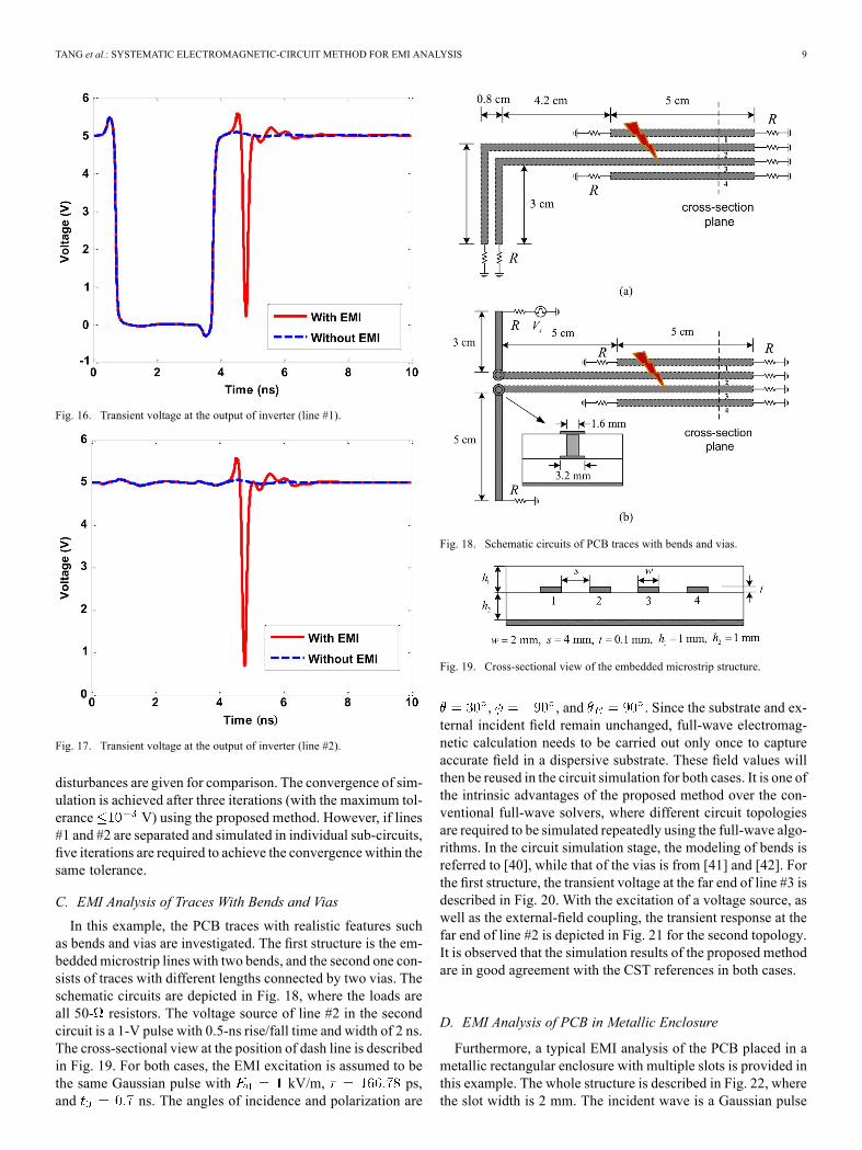
C. EMI Analysis of Traces With Bends and Vias
In this example, the PCB traces with realistic features suchas bends and vias are investigated. The first structure is the em-beddedmicrostrip lines with two bends, and the second one con-sists of traces with different lengths connected by two vias. Theschematic circuits are depicted in Fig. 18, where the loads areall 50- resistors. The voltage source of line #2 in the secondcircuit is a 1-V pulse with 0.5-ns rise/fall time and width of 2 ns.The cross-sectional view at the position of dash line is describedin Fig. 19. For both cases, the EMI excitation is assumed to bethe same Gaussian pulse with kV/m, ps,and ns. The angles of incidence and polarization are
Fig. 18. Schematic circuits of PCB traces with bends and vias.
Fig. 19. Cross-sectional view of the embedded microstrip structure.
, , and . Since the substrate and ex-ternal incident field remain unchanged, full-wave electromag-netic calculation needs to be carried out only once to captureaccurate field in a dispersive substrate. These field values willthen be reused in the circuit simulation for both cases. It is one ofthe intrinsic advantages of the proposed method over the con-ventional full-wave solvers, where different circuit topologiesare required to be simulated repeatedly using the full-wave algo-rithms. In the circuit simulation stage, the modeling of bends isreferred to [40], while that of the vias is from [41] and [42]. Forthe first structure, the transient voltage at the far end of line #3 isdescribed in Fig. 20. With the excitation of a voltage source, aswell as the external-field coupling, the transient response at thefar end of line #2 is depicted in Fig. 21 for the second topology.It is observed that the simulation results of the proposed methodare in good agreement with the CST references in both cases.
D. EMI Analysis of PCB in Metallic Enclosure
Furthermore, a typical EMI analysis of the PCB placed in ametallic rectangular enclosure with multiple slots is provided inthis example. The whole structure is described in Fig. 22, wherethe slot width is 2 mm. The incident wave is a Gaussian pulse

10 IEEE TRANSACTIONS ON MICROWAVE THEORY AND TECHNIQUES, VOL. 61, NO. 1, JANUARY 2013
Fig. 20. Transient voltage at the far end (line #3).
Fig. 21. Transient voltage at the far end (line #2).
Fig. 22. Geometry of a rectangular metallic enclosure.
with kV/m, ps, and ns. It propa-gates in the direction of and with a polariza-tion angle . The cross-sectional geometry of the PCBis depicted in Fig. 23. Like the previous example, two circuittopologies are studied, as shown in Fig. 24. The first structure
Fig. 23. Cross-sectional view of the PCB.
Fig. 24. Schematic circuits of PCB with different topologies.
consists of seven parallel traces with 10-cm length and termi-nated with 50- resistors at the near and far ends. The inputvoltage source of the circuit is a 1-V pulse with a 0.5-ns rise/falltime and a width of 3 ns. The second topology is more com-plicated with different trace lengths, including a bend structure.At the far ends of lines #1 and #4, two diodes in series with10- resistors are terminated. The loads at other ends of thetraces are all 50- resistors. As mentioned in the previous ex-ample, for different circuit topologies we only need to performfull-wave calculation once. Note that in the full-wave simulationwith FDTD algorithm, the thin slots on the metallic enclosureneed special treatment. An improved formulation based on theconformal mapping technique [43] is exploited in this exampleto obtain an exact field distribution near the slot. As mentionedin Section IV, the metallic traces do not need to be consideredwhen computing the excitation fields. Therefore, the computa-tional resource of the proposed method is much less than that ofthe conventional full-wave algorithms where the traces are alsomeshed. To further improve the efficiency, the nonuniform grids[25] are utilized in the calculation of electromagnetic field in thecavity. The minimum and maximummesh sizes are 2 and 5 mm,respectively. The simulation results for the two circuit topolo-gies are shown in Figs. 25 and 26, respectively. For comparison,the results of the full-wave simulator CST are also depicted inthe figures. It is observed that the results of two methods agreewell with each other. For each case, the total simulation time

TANG et al.: SYSTEMATIC ELECTROMAGNETIC-CIRCUIT METHOD FOR EMI ANALYSIS 11
Fig. 25. Transient responses of the first circuit topology. (a) At the far end ofline #1. (b) At the far end of line #4.
of the proposed method is around 4 min, while that of CST ismore than 27 min. Considering the fact that the full-wave sim-ulation needs to be done only once in the proposed method, fur-ther speedup can be achieved.
VI. CONCLUSION
A hybrid method has been proposed for the simulation ofinterconnects on a dispersive substrate with incident field cou-pling. Based on the differential equations derived from the ECMof dispersive media, the full-wave FDTD algorithm is utilizedto capture accurate field surrounding the interconnects. The im-pact of the dispersive dielectric is accurately incorporated in thefield coupling model of transmission lines. The WR-TP tech-nique is employed for efficient simulation of interconnects withdistributed sources. The coupling effects between the lines arerepresented by the equivalent relaxation sources. A simple andclear derivation of the relaxation sources is described in thispaper and the compact results are provided. The accuracy, ef-ficiency, and applicability of the proposed method have beendemonstrated by several benchmark examples.
Fig. 26. Transient responses of the second circuit topology. (a) At the far endof line #1. (b) At the far end of line #4.
APPENDIX
The FDTD algorithm based on ADEs is a typical techniquefor modeling dispersive materials. The ADEs can be obtainedeither by the constitutive relation involving the electric flux den-sity and the electric field intensity [32] or the dynamic evolutionof the polarization parameters excited by the propagating elec-tric field [29]–[31]. A comparison between the latter ADE ap-proach (called the Kashiwa’s method for convenience) and theECM utilized in this paper is given as follows.
A. Debye Media
In [29], differential equations for the Debye medium werewritten in the following state equation form:
(A.1a)
(A.1b)
where is the polarization vector.

12 IEEE TRANSACTIONS ON MICROWAVE THEORY AND TECHNIQUES, VOL. 61, NO. 1, JANUARY 2013
These equations can be extended to the multiterm expressioncases with ease [31], described as follows:
(A.2a)
(A.2b)
By introducing the following relationship:
(A.3)
we can obtain the differential equations (17a) and (17b) pro-posed in Section IV.
B. Lorentz Media
In [31], the curl equations coupled with the ADEs for the th-order Lorentz medium is described by
(A.4a)
(A.4b)
(A.4c)
where is the polarization current density.These equations can be proven to be identical to (23a)–(23c)
by assuming
(A.5a)
(A.5b)
Consequently, from the comparison above, we obtain that dif-ferential equations based on the ECM are equivalent to those inthe Kashiwa’s method.
REFERENCES[1] A. Deutsch et al., “Frequency-dependent losses on high-performance
interconnections,” IEEE Trans. Electromagn. Compat., vol. 43, no. 4,pp. 446–465, Nov. 2001.
[2] A. R. Djordjević, R. M. Biljić, V. D. Likar-Smiljanić, and T. K. Sarkar,“Wideband frequency-domain characterization of FR-4 and time-do-main causality,” IEEE Trans. Electromagn. Compat., vol. 43, no. 4,pp. 662–667, Nov. 2001.
[3] K.M. C. Branch, J. Morsey, A. C. Cangellaris, and A. E. Ruehli, “Phys-ically consistent transmission line models for high-speed interconnectsin lossy dielectrics,” IEEE Trans. Adv. Packag., vol. 25, no. 2, pp.129–135, May 2002.
[4] G. Antonini, A. E. Ruehli, and C. Yang, “PEEC modeling of dispersiveand lossy dielectrics,” IEEE Trans. Adv. Packag., vol. 31, no. 4, pp.768–782, Nov. 2008.
[5] F. M. Tesche, M. V. Ianoz, and T. Karlsson, EMC Analysis Methodsand Computational Models. New York: Wiley, 1997.
[6] C. R. Paul, Analysis of Multiconductor Transmission Lines, 2nd ed.New York: Wiley, 2008.
[7] C. D. Taylor, R. S. Satterwhite, and C. W. Harrison, “The responseof a terminated two-wire transmission line excited by a nonuniformelectro-magnetic field,” IEEE Trans. Antennas Propag., vol. AP-13,no. 6, pp. 987–989, Nov. 1965.
[8] A. K. Agrawal, H. J. Prince, and S. H. Gurbaxani, “Transient responseof multiconductor transmission lines excited by a nonuniform electro-magnetic field,” IEEE Trans. Electromagn. Compat., vol. EMC-22, no.2, pp. 119–129, May 1980.
[9] F. Rachidi, “Formulation of field to field-to-transmission line couplingequations in terms of magnetic excitation,” IEEE Trans. Electromagn.Compat., vol. 35, no. 3, pp. 404–407, Aug. 1993.
[10] I. Maio and F. Canavero, “Analysis of crosstalk and field couplingto lossy MTLs in a SPICE environment,” IEEE Trans. Electromagn.Compat., vol. 38, no. 3, pp. 221–229, Aug. 1996.
[11] I. Erdin, R. Khazaka, and M. Nakhla, “Simulation of high-speed inter-connects in a multilayered medium in the presence of incident field,”IEEE Trans. Microw. Theory Techn., vol. 46, no. 12, pp. 2251–2257,Dec. 1998.
[12] T. Lapohos, J. L. Vetri, and J. Seregelyi, “External field coupling toMTL networks with nonlinear junctions: Numerical modeling and ex-perimental validation,” IEEE Trans. Electromagn. Compat., vol. 42,no. 1, pp. 16–29, Feb. 2000.
[13] G. S. Shinh, N. M. Nakhla, R. Achar, M. S. Nakhla, A. Dounavis, andI. Erdin, “Fast transient analysis of incident field coupling to multicon-ductor transmission lines,” IEEE Trans. Electromagn. Compat., vol.48, no. 1, pp. 57–73, Feb. 2006.
[14] A. R. Sridhar, N. M. Nakhla, R. Achar, M. S. Nakhla, and A. E. Ruehli,“Fast EMI analysis via transverse partitioning and waveform relax-ation,” IEEE Trans. Electromagn. Compat., vol. 51, no. 2, pp. 358–371,May 2009.
[15] G. Antonini, “A spectral formulation for the transient analysis ofplane-wave coupling to multiconductor transmission lines,” IEEETrans. Electronagn. Compat., vol. 51, no. 3, pp. 792–804, Aug. 2009.
[16] A. Dounavis, R. Achar, and M. Nakhla, “Efficient passive circuitmodels for distributed networks with frequency-dependent parame-ters,” IEEE Trans. Adv. Packag., vol. 23, no. 3, pp. 382–392, Aug.2000.
[17] N. M. Nakhla, A. E. Ruehli, M. S. Nakhla, and R. Achar, “Simulationof coupled interconnects using waveform relaxation and transverse par-titioning,” IEEE Trans. Adv. Packag., vol. 29, no. 1, pp. 78–87, Feb.2006.
[18] N. Nakhla, A. E. Ruehli, M. S. Nakhla, R. Achar, and C. Chen, “Wave-form relaxation techniques for simulation of coupled interconnectswith frequency-dependent parameters,” IEEE Trans. Adv. Packag.,vol. 30, no. 2, pp. 257–269, May 2007.
[19] D. Paul, N. M. Nakhla, R. Achar, and M. S. Nakhla, “Parallel simu-lation of massively coupled interconnect networks,” IEEE Trans. Adv.Packag., vol. 33, no. 1, pp. 115–127, Feb. 2010.
[20] B. Gustavsen and A. Semlyen, “Rational approximation of frequencydomain responses by vector fitting,” IEEE Trans. Power Del., vol. 14,no. 3, pp. 1052–1061, Jul. 1999.
[21] D. Saraswat, R. Achar, and M. Nakhla, “A fast algorithm and prac-tical considerations for passive macromodeling of measured/simulateddata,” IEEE Trans. Adv. Packag., vol. 27, no. 1, pp. 57–70, Feb. 2004.
[22] K. M. Coperich, J. Morsey, V. I. Okhmatovski, A. C. Cangellaris, andA. E. Ruehli, “Systematic development of transmission line models forinterconnects with frequency-dependent losses,” IEEE Trans. Microw.Theory Techn., vol. 49, no. 10, pp. 1677–1685, Oct. 2001.
[23] M. Tang and J. F. Mao, “A precise time-step integration method fortransient analysis of lossy nonuniform transmission lines,” IEEE Trans.Electromagn. Compat., vol. 50, no. 1, pp. 166–174, Feb. 2008.
[24] “Hspice User’s Manual” Synopsys Inc., Mountain View, CA, 2007.[Online]. Available: http://www.synopsys.com
[25] A. Taflove and S. C. Hagness, Computational Electrodynamics: TheFinite-Difference Time-Domain Method, 3rd ed. Norwood, MA:Artech House, 2005.
[26] R. Luebbers, F. P. Hunsberger, K. S. Kunz, R. B. Standler, and M.Schneider, “A frequency-dependent finite-difference time-domainformulation for dispersive materials,” IEEE Trans. Electromagn.Compat., vol. 32, no. 3, pp. 222–227, Aug. 1990.
[27] D. F. Kelley and R. J. Luebbers, “Piecewise linear recursive con-volution for dispersive media using FDTD,” IEEE Trans. AntennasPropag., vol. 44, no. 6, pp. 792–797, Jun. 1996.
[28] D. M. Sullivan, “ -transform theory and the FDTD method,” IEEETrans. Antennas Propag., vol. 44, no. 1, pp. 28–34, Jan. 1996.
[29] T. Kashiwa, N. Yoshida, and I. Fukai, “A treatment by the finite-dif-ference time-domain method of the dispersive characteristics associ-ated with orientation polarization,” IEICE Trans., vol. E73, no. 8, pp.1326–1328, 1990.
[30] T. Kashiwa and I. Fukai, “A treatment by FDTD method of dispersivecharacteristics associated with electronic polarization,” Microw. Opt.Technol. Lett., vol. 3, pp. 203–205, 1990.

TANG et al.: SYSTEMATIC ELECTROMAGNETIC-CIRCUIT METHOD FOR EMI ANALYSIS 13
[31] J. L. Young, “Propagation in linear dispersive media: Finite differencetime-domain methodologies,” IEEE Trans. Antennas Propag., vol. 43,no. 4, pp. 422–426, Apr. 1995.
[32] R. M. Joseph, S. C. Hagness, and A. Taflove, “Direct time integra-tion of Maxwell’s equations in linear dispersive media with absorptionfor scattering and propagation of femtosecond electromagnetic pulses,”Opt. Lett., vol. 16, no. 18, pp. 1412–1414, 1991.
[33] A. Rennings, J. Mosig, C. Caloz, D. Erni, and P. Waldow, “Equivalentcircuit (EC) FDTD method for the modeling of surface plasmon basedcouplers,” J. Comput. Theoret. Nanosci., vol. 5, no. 4, pp. 690–703,Apr. 2008.
[34] J. L. Young, A. Kittichartphayak, Y. M. Kwok, and D. Sullivan, “Onthe dispersion errors related to (FD) TD type schemes,” IEEE Trans.Microw. Theory Techn., vol. 43, no. 8, pp. 1902–1909, Aug. 1995.
[35] J. L. Young and R. O. Nelson, “A summary and systematic analysisof FDTD algorithms for linearly dispersive media,” IEEE AntennasPropag. Mag., vol. 43, no. 2, pp. 61–77, Feb. 2001.
[36] P. G. Petropoulos, “Stability and phase error analysis of FD-TD in dis-persive dielectrics,” IEEE Trans. Antennas Propag., vol. 42, no. 1, pp.62–69, Jan. 1994.
[37] L. Zhili and L. Thylen, “On the accuracy and stability of several widelyused FDTD approaches for modeling Lorentz dielectrics,” IEEE Trans.Antennas Propag., vol. 57, no. 10, pp. 3378–3381, Oct. 2009.
[38] Q3D Extractor. ver. 8, Ansoft Corporation, Pittsburgh, PA, 2008. [On-line]. Available: http://www.ansoft.com
[39] CST Studio Suite. Comput. Simulation Technol. (CST), Framingham,MA, 2009. [Online]. Available: www.cst.com
[40] K. C. Gupta, R. Garg, and I. J. Bahl, Microstrip Lines and Slotlines,2nd ed. Norwood, MA: Artech House, 1996.
[41] I. Novak and J. R. Miller, Frequency-Domain Characterization ofPower Distribution Networks. Norwood, MA: Artech House, 2007.
[42] M. Pajovic, “A closed-form equation for estimating capacitance ofsignal vias in arbitarily multilayered PCBs,” IEEE Trans. Electro-magn. Compat., vol. 50, no. 4, pp. 966–973, Nov. 2008.
[43] C. T. Wu, Y. H. Pang, and R. B. Wu, “An improved formalism forFDTD analysis of thin-slot problems by conformal mapping tech-nique,” IEEE Trans. Antennas Propag., vol. 51, no. 9, pp. 2530–2533,Sep. 2003.
Min Tang (M’09) received the B.S. degree in elec-tronic engineering from Northwestern PolytechnicalUniversity, Xi’an, China, in 2001, the M.S. degree inelectrical engineering from Xi’an Jiao Tong Univer-sity, Xi’an, China, in 2004, and the Ph.D. degree inelectronic engineering from Shanghai Jiao Tong Uni-versity, Shanghai, China, in 2007.He is currently a Lecturer with the Department of
Electronic Engineering, Shanghai Jiao Tong Univer-sity. His research interests include modeling and sim-ulation of high-speed interconnects, computer-aided
design (CAD) of very large scale integration (VLSI) circuits, and computationalelectromagnetics.
Jiaqing Lu received the B.S. degree in electronicengineering from Shanghai Jiao Tong University,Shanghai, China, in 2010, and is currently workingtoward the M.S. degree in electronic engineering atShanghai Jiao Tong University.His research interests include EMC and high-speed
interconnects simulation.
Jun-Fa Mao (M’92–SM’98–F’11) was born in1965. He received the B.S. degree in radiationphysics from the University of Science and Tech-nology of National Defense, Hefei, China, in 1985,the M.S. degree in experimental nuclear physicsfrom the Shanghai Institute of Nuclear Research,Shanghai, China, in 1988, and the Ph.D. degree inelectronic engineering from Shanghai Jiao TongUniversity, Shanghai, China, in 1992.Since 1992, he has been a Faculty Member with
Shanghai Jiao Tong University, where he is currentlya Chair Professor and the Executive Dean of the School of Electronic, Informa-tion and Electrical Engineering. From 1994 to 1995, he was a Visiting Scholarwith the Chinese University of Hong Kong, Kowloon, Hong Kong. From 1995to 1996, he was a Postdoctoral Researcher with the University of California atBerkeley. is a Chief Scientist of The National Basic Research Program (973Program) of China, a Project Leader of the National Science Foundation forCreative Research Groups of China, a Cheung Kong Scholar of the Ministryof Education, China, and an Associate Director of the Microwave Society ofChina Institute of Electronics. He has authored or coauthored over 190 journalpapers (including 75 IEEE journal papers) and 120 international conference pa-pers. His research interests include the interconnect and package problem ofintegrated circuits and systems and the analysis and design of microwave cir-cuits.Dr. Mao was the 2007–2009 chair of the IEEE Shanghai Section and the
2009–2012 chair of the IEEE Microwave Theory and Techniques Society(MTT-S) Shanghai Chapter. He was the recipient of the National NaturalScience Award of China (2004), the National Technology Invention Award ofChina (2008), and the Best Paper Award of the 2008 Symposium of APEMCin conjunction with the 19th International Symposium of Zurich EMC.
Lijun Jiang (S’01–M’04) received the B.S. degreein electrical engineering from the Beijing Universityof Aeronautics and Astronautics, Beijing, China, in1993, the M.S. degree from the Tsinghua University,Beijing, China, in 1996, and the Ph.D. degree fromthe University of Illinois at Urbana-Champaign, in2004.From 1996 to 1999, he was an Application Engi-
neer with the Hewlett-Packard Company. From 2004to 2009, he was a Postdoctoral Researcher, ResearchStaff Member, and Senior Engineer with the IBM T.
J.Watson Research Center. Since the end of 2009, he has been an Associate Pro-fessor with the Department of Electrical and Electronic Engineering, Universityof Hong Kong, Kowloon, Hong Kong. He was the Semiconductor Research Co-operation (SRC) Industrial Liaison for several academic projects. He serves asa Reviewer of many primary electromagnetics journals and as special sessionsorganizer for many international conferences. His research interests focus onelectromagnetics, EMC/EMI, antennas, multidisciplinary electronic design au-tomation (EDA) solutions, RF and microwave technologies, and high-perfor-mance computing (HPC).Dr. Jiang has been the SRC Packaging High Frequency Topic TT chair since
2009. He has been a Technical Committee member for IEEE EDAPS since2010. He was a Scientific Committee member of the 2010 IEEE SMEE. Hewas the guest associate editor of a special issue of the IEEE TRANSACTIONSON ANTENNAS AND PROPAGATION. He was the recipient of the 1998 HP STARAward, the 2003 IEEE Microwave Theory and Techniques Society (IEEEMTT-S) Graduate Fellowship Award, the 2004 Y. T. Lo Outstanding ResearchAward, and the 2008 IBM Research Technical Achievement Award.