A Study of Time Amplifiers and Time-to-Voltage Converters...
82
A Study of Time Amplifiers and Time-to-Voltage Converters for Data Conversion Applications By Sung-Min Hong Department of Electrical & Computer Engineering McGill University, Montreal A thesis submitted to McGill University in partial fulfillment of the requirements for the degree of Master of Engineering Copyright ©Sung-Min Hong 2007 December 4, 2007
Transcript of A Study of Time Amplifiers and Time-to-Voltage Converters...

A Study of Time Amplifiers and Time-to-Voltage Converters for Data Conversion Applications
By
Sung-Min Hong
Department of Electrical & Computer Engineering
McGill University, Montreal
A thesis submitted to McGill University in partial fulfillment
of the requirements for the degree of Master of Engineering
Copyright ©Sung-Min Hong 2007
December 4, 2007

Abstract
Time-domain testing remains one of the most challenging obstacles for the semiconductor industry in
mixed-signals testing. With increasing size and complexity of high-performance CMOS integrated circuits
(ICs), conventional production testers are inadequate for today’s high-precision time measurement
requirements as most timing quantities to be measured are often of the same order of magnitude as the timing
resolution of stand-alone measurement devices. To mitigate this problem, the integration of on-chip timing
solutions is required.
Traditional time-to-digital (TDC) converters offer lengthy conversion processes due to incremental
measurement techniques and are not suitable for real-time measurement applications. Moreover, they do not
offer the resolution requirements needed in high-resolution timing verification such as in high-frequency
jitter noise measurement.
This thesis presents a study of the time amplifier (TAMP) circuit used in high-resolution TDC
applications. A detailed description of the time amplification property is discussed and used in the derivation
of several modifications to improve TDC dead time. Further improvements are made by converting the
TAMP to a time-to-voltage converter (TVC) followed by an analog-to-digital converter (ADC). Simulations
show the effects of capacitor configuration and transistor width on conversion-gain and input range.
Signal-to-noise-and-distortion ratio (SNDR) simulations also demonstrate the TVC’s high resolution
capability despite its non-linear behavior and limited dynamic input range. Experimental results from a
discrete implementation of the TVC were then used to confirm behavioral trends seen in simulations.
ii

Abrégé
Le test dans le domaine temporal reste un des obstacles les plus difficiles pour l'industrie de
semi-conducteur dans l'essai de signaux mixtes. Avec l'augmentation de la dimension et de la complexité des
circuits integers (CIs) CMOS à haute performance, les testeurs de production conventionnels sont indéquats
pour les besoins de mesures à haute précision d'aujourd'hui, car la plupart des quantités de synchronisation à
mesurer sont souvent du même ordre de grandeur que la résolution de synchronisation des dispositifs
autonomes de mesure. L'intégration de solutions de synchronisation de sur-morceau est exigée pour résoudre
ce problème.
Les convertisseurs temps à code numérique (CTN) traditionnels offrent des processus prolongés de
conversion dus aux techniques par accroissement de mesure et donc, ne sont pas appropriés aux applications
en temps réel de mesure. D'ailleurs, ils n'offrent pas les conditions de résolution requises dans la vérification
à haute résolution de synchronisation comme dans la mesure de bruit de vacillement à haute fréquences.
Cette dissertation présente une étude du circuit d’amplificateur de temps (TAMP) utilisé dans des
applications à haute résolution de CTN. Une description détaillée de la propriété d'amplification de temps est
discutée et employée dans la dérivation de plusieurs modifications pour améliorer le temps mort du CTN.
D'autres améliorations sont apportées en convertissant le TAMP en convertisseur de temps-à-voltage (TVC)
suivi d'un convertisseur analogique-numérique (CAN). Les simulations démontrent les effets de la
configuration des condensateurs et de la largeur des transistors sur le gain et la gamme des signaux entrants.
Les simulations de rapport signal sur bruit et distortion (RSBD) démontrent également les possibilités de
haute résolution du CTN en dépit de son comportement non linéaire et d’une gamme dynamique limitée des
signaux entrants. Des résultats expérimentaux d’une mise en œuvre à composants distincts du CTN ont été
alors employés pour confirmer les tendances fonctionnelles déduites par les simulations.
iii

Acknowledgements
The time has finally come for me to submit my Masters thesis and close a pivotal chapter in my academic
life. I thank God for giving me the ability and strength to complete this academic endeavor. Although my time
as a graduate student has brought me great memories, the past three years was a very difficult and confusing
time for me, and at moments, I did not know if I had the courage to continue. Luckily, I had the fortune of
having a great support group without which I would have never seen the light at the end of the tunnel and I
owe this work to these people.
First and foremost, I would like to thank my supervisor Professor Gordon W. Roberts for giving me the
opportunity to be part of his research group. I am eternally grateful for his guidance, knowledgeable advice
and encouraging words, which were instrumental to my research. His keen insight and industry experience
has really helped me understand the importance of practicality when approaching research. Furthermore, his
never-ending enthusiasm and true appreciation for the sciences will always be a source of inspiration. And I
will never forget his tales of his experience at a startup. Because of him, I will always exert a little more
caution when in comes to dealing with the sharks of the corporate world.
Secondly, I would like to say a special word of gratitude to Professor Anas Hamoui who has helped me
guide through the early stages of my research when no sense of direction seemed in sight. He has always kept
his door open for his students and I will forever be thankful for the length at which he would go to lend a
helping hand.
I would also like to thank the numerous friendships I have developed over the course of my Masters. In
particular: Dani Tannir (Dano), Tarek Alhajj (Trek), Kelvin Lee (The Kelvin), Sadok Aouini (Madcoco), Jeff
Koo (Captain Jeef), Cristian Radita (Cristi), Ahmed Abdelaaty (Koosh), Usman Khalid (Ozman), Baker
Haddadin (The Beaver), Terence Kao, Mohammad Taherzadeh, Arash Khajooeizadeh, Youssed El-Kurdi,
Kun Chuai, Carmen Au, Mourad Oulmane, and Mona Safi-Harb. These people are like family to me and
helped me countless times along the way, especially when I needed them the most. They have also kept me
quite entertained throughout the years and have brought a lot funny memories which I can never forget.
I want to also extend my gratitude to my friends Olivier Morais and Michel Ha-Thanh. They have been
the best of friends since high-school and are still to this day. They have shown me life outside of school and
were my council throughout the course of my degree.
Next, I want to thank my brother and fellow engineer, David. He has taught me everything I know and has
been my library of knowledge. He has helped me become the very best I can be to succeed in my studies. A lot
of what I know today, is because of his teachings.
And finally, I would like to thank my parents, Wooyoung and Myung Jae, who have been a source of
endless support. They have given me so much and I, so little. I would not be where I am today if it were not
for all the sacrifices they have made for me and for that, I will always be in their debt. This degree is dedicated
iv

to them.
v

Table of Contents
Abstract ii
Abrégé iii
Acknowledgements iv
List of Figures ix
List of Tables xii
List of Abbreviations xiii
Chapter 1 Introduction 1 1.1 MOTIVATION ....................................................................................................................................... 1
1.2 ON-CHIP MIXED-SIGNALS TEST CORE ................................................................................................ 2
1.3 TIME-DOMAIN ANALYSIS .................................................................................................................... 3
1.4 THESIS ORGANIZATION ....................................................................................................................... 4
Chapter 2 Time-to-Digital Architecture Review 5 2.1 INTRODUCTION .................................................................................................................................... 5
2.2 SINGLE COUNTER (COARSE TDC) ....................................................................................................... 5
2.3 PULSE-SHRINKING TDC ...................................................................................................................... 6
2.4 PULSE-STRETCHING (DUAL-SLOPE CONVERSION) ............................................................................... 7
2.5 FLASH TDC ......................................................................................................................................... 9
2.6 VERNIER DELAY LINE (VDL) .............................................................................................................. 9
2.6.1 Mutliple VDLs .............................................................................................................................. 9
2.6.2 Single-Stage VDL ....................................................................................................................... 10
2.7 SUMMARY ......................................................................................................................................... 11
Chapter 3 Time Amplifier Circuit Architecture 12
vi

3.1 INTRODUCTION .................................................................................................................................. 12
3.2 TIME AMPLIFIER-BASED TDC ARCHITECTURE ................................................................................. 12
3.3 TIME AMPLIFICATION ........................................................................................................................ 13
3.3.1 Case 1: ΔΦin >> 1 ..................................................................................................................... 15
3.3.2 Case 2: ΔΦin << 1 ..................................................................................................................... 16
3.4 TIME AMPLIFIER CIRCUIT .................................................................................................................. 17
3.5 IMPROVED TIME AMPLIFIER CIRCUIT ................................................................................................ 19
3.6 IMPROVED TIME AMPLIFIER BEHAVIORAL CHARACTERISTICS .......................................................... 21
3.6.1 Capacitors C1=C2 Sweep ........................................................................................................... 21
3.6.2 Capacitors C2/C1 Sweep ............................................................................................................ 23
3.6.3 Load Resistor RD Sweep ............................................................................................................. 24
3.6.4 Transistor Width W Sweep ......................................................................................................... 25
3.7 TIME AMPLIFIER SHORTCOMINGS ...................................................................................................... 26
3.8 SUMMARY ......................................................................................................................................... 29
Chapter 4 Development of Time Amplifier-Based Time-to-Voltage Converter 30 4.1 INTRODUCTION .................................................................................................................................. 30
4.2 PROPOSED TVC-BASED TDC ............................................................................................................ 30
4.3 PROPOSED TAMP-BASED TVC CIRCUIT ........................................................................................... 31
4.4 TVC BEHAVIORAL CHARACTERIZATION ........................................................................................... 37
4.4.1 Capacitor C1 = C2 Sweep ............................................................................................................ 38
4.4.2 Capacitor C2/C1 Sweep .............................................................................................................. 43
4.4.3 Transistor Width W Sweep ......................................................................................................... 45
4.5 SUMMARY ......................................................................................................................................... 47
Chapter 5 Experimental Results 48 5.1 INTRODUCTION .................................................................................................................................. 48
5.2 DISCRETE TVC DESIGN ..................................................................................................................... 48
5.3 EXPERIMENT SETUP ........................................................................................................................... 49
5.4 EXPERIMENTAL RESULTS .................................................................................................................. 52
5.5 TRANSFER CHARACTERISTIC TESTING ............................................................................................... 54
5.6 DNL AND INL TESTING .................................................................................................................... 56
5.6.1 TAMP-Based TVC Configuration 1: C1 = C2 = 2.2 nF ............................................................. 57
5.6.2 TAMP-Based TVC Configuration 2: C1 = C2 = 5.6 nF ............................................................. 58
5.6.3 TAMP-Based TVC Configuration 2: C1 = 2.2 nF, C2 = 5.6 nF ................................................ 60
5.6.4 INL and DNL Summary ............................................................................................................. 62
vii

5.7 SUMMARY ......................................................................................................................................... 63
Chapter 6 Conclusions and Future Research 64 6.1 CONCLUSIONS ................................................................................................................................... 64
6.2 FUTURE RESEARCH ........................................................................................................................... 65
6.2.1 IC Implementation ..................................................................................................................... 65
6.2.2 Calibration ................................................................................................................................. 66
6.2.3 Asymmetrical TVC Design ......................................................................................................... 66
References 68
viii

List of Figures
Figure 1.1 Teradyne Flex SOC Tester ........................................................................................................... 2
Figure 1.2 Tester IC Interfaced with DUT ..................................................................................................... 3
Figure 1.3 Tester IC Integrated with DUT in a Single Chip .......................................................................... 3
Figure 2.1 Single Counter TDC Implementation ........................................................................................... 6
Figure 2.2 Inverter Chain Example of Pulse-Shrinking Effect ...................................................................... 6
Figure 2.3 Pulse-Shrinking TDC Architecture ............................................................................................... 7
Figure 2.4 Pulse-Stretching TDC Architecture .............................................................................................. 7
Figure 2.5 Pulse-Stretching Sample Timing Diagram ................................................................................... 8
Figure 2.6 Daisy Chain Flash Converter ....................................................................................................... 9
Figure 2.7 Multiple Vernier Delay Lines ..................................................................................................... 10
Figure 2.8 Single-Stage Vernier Delay Line ................................................................................................ 10
Figure 3.1 Traditional Voltage-Based ADC Architecture ........................................................................... 13
Figure 3.2 Time Amplifier-Based TDC Architecture ................................................................................... 13
Figure 3.3 Conceptual Model of Time Amplifier ......................................................................................... 14
Figure 3.4 Example Timing Diagram of the Time Amplifier ....................................................................... 15
Figure 3.5 TAMP Timing Diagram for ΔΦin >> 1 ...................................................................................... 16
Figure 3.6 TAMP Timing Diagram for ΔΦin << 1 ...................................................................................... 17
Figure 3.7 Original TAMP OTA Circuit ...................................................................................................... 17
Figure 3.8 Sample TAMP OTA Output ........................................................................................................ 18
Figure 3.9 Improved TAMP OTA Circuit .................................................................................................... 20
Figure 3.10 Simplified TAMP OTA Model in Phase I ................................................................................. 20
Figure 3.11 Simplified TAMP OTA Model in Phase II ................................................................................ 21
Figure 3.12 Improved TAMP Transfer Curves for Capacitor C1 = C2 Sweep (RD = 36 kΩ,
W = 80 μm, Tr = 250 psec) ...................................................................................................... 22
Figure 3.13 Improved TAMP OTA Transient for ΔΦin = 200 psec and C1 = C2 = 1 pF (RD = 36 kΩ,
W = 80 μm, Tr = 250 psec) ...................................................................................................... 22
Figure 3.14 Improved TAMP OTA Transient for ΔΦin = 200 psec and C1 = C2 = 4 pF (RD = 36 kΩ,
W = 80 μm, Tr = 250 psec) ...................................................................................................... 23
Figure 3.15 Improved TAMP Transfer Curves for Capacitor C2/C1 Sweep (C1 = 4 pF, RD = 36kΩ,
W = 80 μm, Tr = 250 psec) ...................................................................................................... 24
Figure 3.16 Improved TAMP Transfer Curves for Load Resistor RD Sweep (C1 = C2 = 4 pF, W = 80 μm,
Tr = 250 psec) .......................................................................................................................... 25
ix

Figure 3.17 Improved TAMP Transfer Curves for Transistor Width W Sweep (C1 = C2 = 4 pF, RD = 36 kΩ,
Tr = 250 psec) .......................................................................................................................... 26
Figure 3.18 Effects of TAMP Gain on Output Intersection Angles and PID Evaluation ............................. 27
Figure 3.19 CMOS Arbiter Used as PID Circuit [11] ................................................................................. 28
Figure 3.20 Sample Timing Diagram for TAMP-Based TDC with Single-Stage VDL ................................ 28
Figure 4.1 Time-to-Voltage Converter-Based TDC Architecture ................................................................ 31
Figure 4.2 Effects of ΔΦin on TAMP Vout1+ Transient (C1 = C2 = 4 pF, RD = 36 kΩ, W = 80 μm,
Tr = 250 psec) .......................................................................................................................... 32
Figure 4.3 Effects of ΔΦin on TAMP Vout2+ Transient (C1 = C2 = 4 pF, RD = 36 kΩ, W = 80 μm,
Tr = 250 psec) .......................................................................................................................... 33
Figure 4.4 Improved TAMP OTA Transient for ΔΦin = 150 psec (C1 = C2 = 4 pF, RD = 36 kΩ, W = 80 μm,
Tr = 250 psec) .......................................................................................................................... 33
Figure 4.5 TAMP-base TVC Circuit ............................................................................................................ 34
Figure 4.6 Simplified TVC Model ................................................................................................................ 35
Figure 4.7 TAMP-based TVC Transient for ΔΦin = 200 psec (C1 = C2 = 4 pF, W = 80 μm, Tr = 250 psec)
................................................................................................................................................. 36
Figure 4.8 TAMP-base TVC Transfer Curve (C1 = C2 = 1 pF, W = 80 μm, Tr = 250 psec) ........................ 36
Figure 4.9 Sinusoidal Phase Modulated Clock Input .................................................................................. 37
Figure 4.10 TAMP-Based TVC Differential Voltage Signal, Distortion and Noise Plots for Capacitor
C1 = C2 Sweep (W = 80 μm, Tr = 250 psec) ............................................................................ 39
Figure 4.11 TAMP-Based TVC SNDR Plot for Capacitor C1 = C2 Sweep (W = 80 μm, Tr = 250 psec) .... 40
Figure 4.12 Effects of Small and Large ΔΦin on TVC Transient Output ..................................................... 42
Figure 4.13 TAMP-Based TVC Differential Voltage Signal, Distortion and Noise Plots for Capacitor C2/C1
Sweep (C1 = 1 pF, W = 80 μm, Tr = 250 psec) ........................................................................ 44
Figure 4.14 TAMP-Based TVC SNDR Plot for Capacitor C2/C1 Sweep (C1 = 1 pF, W = 80 μm,
Tr = 250 psec) ......................................................................................................................... 45
Figure 4.15 TAMP-Based TVC Differential Voltage Signal, Distortion and Noise Plots for Transistor Width
W Sweep (C1 = C2 = 2.8 pF, Tr = 250 psec)............................................................................ 46
Figure 4.16 TAMP-Based TVC SNDR Plot for Transistor Width W Sweep (C1 = C2 = 2.8 pF, Tr = 250 psec)
................................................................................................................................................. 47
Figure 5.1 Discrete TVC Circuit Schematic ................................................................................................ 49
Figure 5.2 Discrete TVC Circuit on Vector Prototype Board ...................................................................... 49
Figure 5.3 TVC Test Bench Schematic ......................................................................................................... 50
Figure 5.4 TVC Test Bench Setup ................................................................................................................ 50
Figure 5.5 TVC Test Bench Timing Diagram .............................................................................................. 51
Figure 5.6 FPGA Logic Block Diagram for Reset Clock Generation ......................................................... 52
x

Figure 5.7 Oscilloscope Screen Capture of TVC Output with No Averaging (∆Φin=10nsec, C1=C2=2.2nF)
................................................................................................................................................. 53
Figure 5.8 Noise Histogram for TVC Differential Output ∆Vout (∆Φin=10nsec, C1=C2=2.2nF)................. 53
Figure 5.9 Oscilloscope Screen Capture of TVC Output with 4096-Point Running Average (∆Φin=10nsec,
C1=C2=2.2nF) ......................................................................................................................... 54
Figure 5.10 Discrete TAMP-Based TVC Transfer Curve for C1=C2=2.2nF ............................................... 55
Figure 5.11 Discrete TAMP-Based TVC Transfer Curve Comparison ....................................................... 56
Figure 5.12 Discrete TAMP-Based TVC Linear Region and Best-Fit-Line (C1 = C2 = 2.2 nF) ................. 57
Figure 5.13 DNL Curve within Linear Region of Discrete TAMP-Based TVC (C1 = C2 = 2.2 nF) ............ 58
Figure 5.14 INL Curve within Linear Region of Discrete TAMP-Based TVC (C1 = C2 = 2.2 nF) .............. 58
Figure 5.15 Discrete TAMP-Based TVC Linear Region and Best-Fit-Line (C1 = C2 = 5.6 nF) ................. 59
Figure 5.16 DNL Curve within Linear Region of Discrete TAMP-Based TVC (C1 = C2 = 5.6 nF) ............ 59
Figure 5.17 INL Curve within Linear Region of Discrete TAMP-Based TVC (C1 = C2 = 5.6 nF) .............. 60
Figure 5.18 Discrete TAMP-Based TVC Linear Region and Best-Fit-Line (C1 = 2.2 nF, C2 = 5.6 nF) ..... 61
Figure 5.19 DNL Curve within Linear Region of Discrete TAMP-Based TVC (C1 = 2.2 nF, C2 = 5.6 nF) 61
Figure 5.20 INL Curve within Linear Region of Discrete TAMP-Based TVC (C1 = 2.2 nF, C2 = 5.6 nF) . 62
Figure 6.1 Generation of TVC Reset Clock for Periodic Inputs with Even-Matching ................................. 65
Figure 6.2 Generation of TVC Reset Clock for Aperiodic Inputs with Even-Matching ............................... 66
Figure 6.3 Asymmetrical TAMP-based TVC Circuit ................................................................................... 67
Figure 6.4 Asymmetrical TVC Architecture with Arbiter Data Selection .................................................... 67
xi

List of Tables
Table 5.1 TAMP-Based TVC Configurations Summary (LSB = 100 psec) ................................................... 63
xii

xiii
List of Abbreviations
ADC Analog-to-Digital Converter
DIB Device-Interface Board
DNL Differrential Nonlinearity
DUT Device-under-Test
IC Integrated Circuits
INL Integral Nonlinearity
LR-TDC Low-Resolution Time-to-Digital Converter
MUTEX Mutually Exclusion
OTA Operational Transconductance Amplifier
PID Phase/Polarity Inversion Detector
TAMP Time amplifier
TDC Time-to-Digital Converter
TVC Time-to-Voltage Converter

Chapter 1
Introduction
1.1 Motivation
During the past couple of years, the development of rapid and cost-effective analog and mixed-signals
testing techniques has gain considerable momentum in the semiconductor industry. This is in part due to the
increasing degree of complexity prevalent in digital and analog circuit designs as well as increasing speed
requirements seen in today’s high-performance application areas such as in communications, computers and
video technologies. The success of these applications is determined by their level of quality and reliability,
which requires the integration of comprehensive test methodologies and tools into design and test
environments.
Traditionally, CMOS integrated circuits (ICs) are tested using a production tester such as the Teradyne
Flex SOC in Figure 1.1. The device-under-test (DUT) makes contact with the device-interface board (DIB) of
the test head via the handlers or probers, which are essentially electrical pins. These pins are then used to both
excite the DUT with various analog or digital test patterns and capture the output into the tester’s memory.
Although in the past, these types of production testers were more than capable of capturing very accurate
measurements from the DUT, recent progresses in IC technology has lead tester’s measurement capabilities
to be inadequate. This is because, in the past, the test equipments were often designed using
high-performance technologies such as silicon bipolar and gallium arsenide (GaAs), which often
outperformed the speed and noise performance of CMOS technology [21]. In addition, with the down-scaling
of CMOS devices to sub-micron dimensions and GHz operating speeds, issues like signal integrity and jitter
noise become of growing concern and cannot be neglected.
The 2005 edition of the International Technology Roadmap for Semiconductor has stated that one of the
1

most difficult challenges that need to be addressed in the upcoming years is the timing jitter measurement in
high-speed VLSI systems [8]. With clock frequencies expected to go as high as in the tens of GHz by 2010,
most timing quantities to be measure on-chip can be of the same order of magnitude as the timing resolution
of the measurement device. Examples of such are in the measurement of jitter noise in phase locked loops
(PLLs) [7] and in sampling clock jitter in analog-to-digital converters (ADCs) [19].Therefore, there is a need
for sophisticated high-precision time measurement circuits such as the Time-to-Digital Converters (TDCs).
Figure 1.1 Teradyne Flex SOC Tester
1.2 On-Chip Mixed-Signals Test Core
Historically, the production cost of custom ICs has continued to drop dramatically alongside the growth
of the ASIC industry, while the costs associated with testing have been steadily increasing. These costs are
tied to high specification requirements in today’s verification environment such as tester speed, accuracy, pin
count, and vector depth [21]. However, despite the high cost of high-speed mixed-signals testing, the use of
even the most advanced production testers for timing measurements can pose significant problems since the
large electrical distances between the DUT and the tester can cause attenuation effects and phase delay errors
for high-speed signals. Furthermore, the routing of deeply buried signals inside the chip core to the output
pins is not practical and can cause timing skew.
2

To remedy the situation, timing measurement circuits can be implemented on IC and interfaced to the
DUT on the DIB as shown in Figure 1.2. This reduces the distance between the tester circuit and the DUT and
improves overall measurement accuracy, while also reducing test cost. Another solution for efficient low-cost
mixed-signals testing technique is the implementation of the test core on the same silicon die as the DUT as
depicted in Figure 1.3. This technique further reduces any electrical distance between the two circuits and
rendering high-frequency timing measurements possible. Moreover, implementation of both circuits in a
single IC is the added benefit of improved accessibility to buried nodes within the DUT. This can effectively
reduce the number of output pins on the IC and thereby, saving testing costs.
Figure 1.2 – Tester IC Interfaced with DUT
Figure 1.3 Tester IC Integrated with DUT in a Single Chip
1.3 Time-Domain Analysis
Another motivation for the need of high-precision time measurement devices is for time-domain
applications. With rapid evolution in digital integrated technology aiming towards increase in speed, higher
performance and greater miniaturization, noise and interference levels become significant detrimental factors
in signal integrity requiring the need for sophisticated signal processing techniques. Time-to-Digital
Converters (TDCs) present numerous advantages over conventional voltage-based Analog-to-Digital
3

converters (ADC’s). TDCs can offer greater immunity to noise and interference, wider dynamic range,
process scalability as well as simplicity in design and integration [1]. Some important applications of TDCs
are in time-of-flight (TOF) laser radars for distance and velocity measurements [3], RF synthesizers [4],
calibration of automatic test equipment systems [5] and telecommunication applications such as PM and FM
demodulators [6]. However, some applications can pose more challenge than others, thereby demanding
stringent requirements on TDC designs.
1.4 Thesis Organization
In this research work, we present the development of a low-complexity TAMP-based Time-to-Voltage
Converter (TVC) for TDC applications. Chapter 2 of this thesis introduces a literary survey of current TDC
architectures. An in depth overview of the TAMP circuit architecture is then discussed in Chapter 3.
In Chapter 4, a new TAMP-based TVC circuit is proposed and its behavior examined. This is then followed
by experimental results from a discrete prototype circuit board in Chapter 5. And finally, some future work
and brief conclusion is presented in Chapter 6.
4

Chapter 2
Time-to-Digital Architecture Review
2.1 Introduction
This chapter serves to present an overview of the most common type of time measurement techniques
used for TDC applications such as the Single Counter, Pulse-Shrinking, Pulse-Stretching, Flash TDC, and
Vernier Delay Lines. Each of the TDC architectures will be discussed as well as some of their weaknesses.
2.2 Single Counter (Coarse TDC)
Perhaps the simplest oldest and simplest TDC architecture is the Single Counter TDC implementation
shown in Figure 2.1 [15]. This converter operates by counting the number of clock cycles fitting in the time
interval set between the START and STOP signal. A significant drawback to this architecture is the
limitations set by the reference clock. Because the resolution of this TDC is equivalent to a single clock
period, high speed clocks are desirable. For on-chip applications, restrictions set on clock frequency seriously
limit the Single Counter TDC from being used for high-resolution applications. However, this system is often
used as a supplementary block to higher resolution TDC systems to allow coarse measurements and extend
the input dynamic range [15].
5

Figure 2.1 Single Counter TDC Implementation
2.3 Pulse-shrinking TDC
Another simple TDC architecture is the cyclic pulse-shrinking TDC. This type of converter measures the
width of an incoming pulse through the use of a pulse-shrinking element. A simple example of this is a chain
of inverters depicted in Figure 2.2 [12]. Assume all inverters are identical except for one gate, which is
denoted as the pulse-shrinking element. By carefully designing the aspect ratio W/L of this single inverter,
the rise and fall times can be altered to differ from all others in the chain and offer an incremental reduction in
pulse width [13]. Although in this example, only one shrinking element was used, any number of shrinking
elements can be used to provide a combined effect.
Figure 2.2 Inverter Chain Example of Pulse-Shrinking Effect
The overall pulse-shrinking TDC architecture is shown in Figure 2.3. In this architecture, the overall pulse
width is found by cycling the pulse through the pulse-shrinking element and counting the number of cycles
required to reduce the pulse until it can no longer propagate through the chain. Notice that in this particular
design, the shrinking element has been chosen to be the front-end coupling stage since it is naturally designed
to be the different block in the loop.
6

Figure 2.3 Pulse-Shrinking TDC Architecture
One common problem with this type of design is the long dead time since the measurement of the
incoming pulse width is directly dependent on the number of cycles in the loop. Therefore, although this
suggests to an almost unlimited input range, the dead times can become increasingly significant for larger
inputs rendering this architecture impractical for repeated measurements. Another problem with this TDC is
its sensitivity to temperature, which can affect both carrier mobility and threshold voltage of a MOS transistor
requiring the need for a careful calibration technique [14].
2.4 Pulse-stretching (Dual-Slope Conversion)
Opposite to pulse-shrinking, the pulse-stretching technique digitizes an incoming pulse by stretching the
pulse to a more detectable level and using a measurement clock to count. The full pulse-stretching
architecture is shown in Figure 2.4 [2].
Figure 2.4 Pulse-Stretching TDC Architecture
The stretch factor is implemented as a product of a current ratio and a capacitor ratio to minimize for
process variability. Prior to any measurement, the capacitors C1 and C2 are reset and at the arrival of a pulse,
C1 starts discharging with a constant current I1. At the falling edge of the pulse, C1 stops discharging and a
7

larger capacitor C2 = M·C1 discharges with a smaller current I2 = I1/N as described by the following
relationship
(1)
where ΔV1 and ΔV2 describe the change in voltage on capacitors C1 and C2 respectively. ΔT1 and ΔT2
represent the discharge period for capacitors C1 and C2 respectively.
At this point, the comparator is enabled and the counter starts counting the number of clock cycles until
the voltage on both capacitors are equal. Equation 2 shows that the initial pulse width does in fact stretch by
a factor of M·N and the LSB width of this TDC architecture is TCLK/(M·N). Figure 2.5 shows a sample timing
diagram of the Pulse-Stretching TDC.
(2)
Figure 2.5 Pulse-Stretching Sample Timing Diagram
8

2.5 Flash TDC
Analogous to flash ADCs, flash TDCs operate by comparing a signal edge to various reference signal
edges displaced in time. Whereas in the case of the flash ADC, voltage comparisons are made by a
comparator, its equivalent in the time-domain is the arbiter, which decides which of two inputs signal arrived
first. The most basic form of an arbiter is the edge-triggered flip-flop. An example of a daisy chain flash
converter is shown in Figure 2.6 [17]. The STOP signal is compared to different delayed versions of the
START signal with the help of identical delay buffers. This then generates a thermometer coded output which
indicates the input time difference within one buffer delay τ. Therefore, the highest resolution achievable by
this architecture is one buffer delay. The delay is often known and controlled by using voltage-controlled
buffers stabilized by a delay-locked loop to compensate for temperature or supply voltage changes as well as
process variations [18]. Although, the Flash TDC can be used for medium resolution applications, this type of
converter is not always useful for on-chip jitter measurement applications where results are often at sub-gate
resolutions.
Figure 2.6 Daisy Chain Flash Converter
2.6 Vernier Delay Line (VDL)
2.6.1 Mutliple VDLs
Multiple Vernier Delay Lines can overcome the limitation in temporal resolution of the Flash TDC by
adding a second chain of buffers at the STOP input as seen in Figure 2.7 [22][16]. Notice that the second
chain has a delay τf different from that of the first chain defined as τs. While τf denotes a faster buffer (i.e.
shorter delay), τs denotes a slower buffer (i.e. longer delay). By controlling these delays to be close to each
other, sub-gate resolutions are possible with the VDL structure. Similar to the Flash TDC, the output is
thermometer coded and the input time difference is defined in Equation 3, where N represents the location of
the first latched arbiter.
9

Figure 2.7 Multiple Vernier Delay Lines
(3)
The effective time resolution achieved in a VDL-based TDC equals the delay difference between the two
buffers τs–τf. This resolution is good as the matching between the various buffer cells. However, in order to
have larger input range, a large number of VDLs must be used, which leads to mismatching problems. Even
with careful layout techniques, the mismatches cannot be completely eliminated.
2.6.2 Single-Stage VDL
The Single-Stage VDL eliminates any mismatch problems by replacing the delay chain by a single delay
element in a ring oscillator configuration as shown in Figure 2.8 [22]. The frequencies of both oscillators are
kept close to maximize resolution. At the arrival of the START signal, the first ring oscillator is triggered and
generates a constant clock period. Once the STOP signal arrives, it triggers the second oscillator and activates
the counter. Because the two oscillators have slightly different frequencies, the second oscillator will catch up
to the first in phase allowing the phase detector to detect the moment of phase coincidence between the two
oscillators while the counter records the elapsed number of clock cycles.
Figure 2.8 Single-Stage Vernier Delay Line
In contrast to other methods, the VDL structure is able to resolve very fine sub-gate time differences.
Although this type of TDC removes all mismatch problems, it still has the problem of process, voltage and
10

temperature sensitivity in the oscillators. Therefore, careful calibration techniques must be in place to resolve
the exact time difference between the two oscillators. Moreover, because the VDL architecture is limited to
inputs smaller than τs, it often needs to be used in conjunction with a coarser time measurement circuit.
2.7 Summary
This chapter gives a summary of the different time measurement techniques seen in current literature.
Some of the input range limitations and long conversion times common to these TDC architectures were also
discussed.
11

Chapter 3
Time Amplifier Circuit Architecture
3.1 Introduction
An ideal TDC is often qualified as having a wide dynamic range, high resolution and a robust calibration
process immune to Process, Voltage and Temperature (PVT) variations. The purpose of this chapter is to
introduce an innovative TDC architecture based on the Time Amplifier (TAMP) block described in [9],
which can overcome some of the shortcomings seen in past traditional TDC techniques such as the ones
discussed in the previous chapter. Following a detailed analysis of the TAMP circuit, simplifications and
improvements are proposed to the existing circuit. In addition, parametric simulations are performed to study
the effects of various circuit parameters and potential drawbacks of the TAMP-based TDC architecture are
discussed.
3.2 Time Amplifier-Based TDC Architecture
Voltage amplifiers are considered to be one of the most basic and fundamental building blocks in ADC
designs. Its importance comes from its ability to magnify small voltage differences to alleviate some of the
stringent requirements necessary for high-resolution voltage-based ADC architectures such as the classic one
shown in Figure 3.1. Similarly, this concept can be ported to the time domain by introducing the time
amplifier. Just like its analog counterpart, the time amplifier functions by enlarging small input time
differences set by two time events, generally in the form of two rising edge signals. This amplification
process helps mitigate some of the input range problems found in most high-resolution TDC designs. The
time amplifier represents a key block in the TAMP-based TDC architecture since, as a front-end block, its
characteristics can set the overall performance of the converter. By introducing the TAMP, high-resolution
12

TDC designs no longer suffer from strict time resolution requirements. Furthermore, this type of architecture
simplifies TDC designs by allowing a wide range of Low Resolution Time-to-Digital Converters (LR-TDC)
to be used in conjunction with the TAMP for high-resolution measurements. In fact, any of the TDC
architectures reviewed in Chapter 2 can be used as the LR-TDC. The TAMP-based TDC is shown in Figure
3.1, where the two input time events are defined as Φin1 and Φin2.
Figure 3.1 Traditional Voltage-Based ADC Architecture
Figure 3.2 Time Amplifier-Based TDC Architecture
3.3 Time Amplification
The notion of time amplification was first introduced in [10] by using Mutual Exclusion (MUTEX)
elements to enlarge input time differences. This design was further improved with a differential circuit
structure in [9]. Conceptually, the TAMP is a fully analog circuit constituting of two cross-coupled
Operational Transconductance Amplifiers (OTAs) followed by a pair of Phase/Polarity Inversion Detectors
(PIDs) as shown in Figure 3.3.
13

The cross-coupled OTA stage is mainly responsible for the time amplification behavior and functions by
converting the time/phase difference between two time-triggered events, Φin1 and Φin2, into two differential
voltage signals, Vout1 and Vout2 defined as
(4)
(5)
The differential output from the cross-coupled OTAs are then fed into a PID circuit which detects the
phase inversion between Vout1,2+ and Vout1,2- and generates two separate rising edge signals, Φout1 and Φout2,
corresponding to the newly amplified time difference now measurable by a LR-TDC as shown in a sample
timing diagram in Figure 3.4.
Figure 3.3 – Conceptual Model of Time Amplifier
14

Figure 3.4 – Example Timing Diagram of the Time Amplifier
The input and output time differences, ΔΦin and ΔΦout, are defined respectively as
(6)
(7)
In order to gain a better understanding of the TAMP circuit behavior, the following two operating cases
are considered:
3.3.1 Case 1: ΔΦin >> 1
For the first case, a large input phase difference signal is assumed. In other words, the second input signal
Φin2 arrives once the OTA1 has finished settling from the first input signal Φin1. Note that prior to the arrival
of the first edge, both differential voltages, Vout1 and Vout2, are initially set to low.
At the arrival of the first time event Φin1, the first differential pair will swing its output voltage Vout1 from
low to high. This voltage is then fed into a comparator, where it detects a polarity inversion and generates the
first output phase signal Φout1 denoted as the output reference phase. Note that the occurrence of the reference
phase Φout1 is solely dependent on the natural response of the OTA1 and Φin1. Similarly, the second time
event Φin2 will generate a second phase signal Φout2 denoted as the measurement phase. Since we assumed
steady state for Vout1 prior to the arrival of Φin2, Φout2 is only dependent on the natural response of the OTA
and Φin2. Note that for this example, both Φin1 and Φin2 are assumed to be larger than Vout1- and Vout2-
15

respectively in order swing the differential pairs in the OTA for a proper phase inversion.
In this particular case, no interdependencies exist between both output signals since each output depends
only on its corresponding phase inputs and its corresponding OTA’s natural response behavior. Thus, the
resulting output time interval ΔΦout does not receive any amplification. As a result, an upper limit can be
established on the input dynamic range of the TAMP circuit. Figure 3.5 shows a timing diagram of the TAMP
circuit for large ΔΦin, where TOTA1 and TOTA2 are constants corresponding to the natural response times of
OTA1 and OTA2 respectively.
Figure 3.5 – TAMP Timing Diagram for ΔΦin >> 1
3.3.2 Case 2: ΔΦin << 1
In the second case, a small phase input is assumed, that is, the second phase input Φin2 is received prior to
the first phase output Φout1 reaching steady-state. For such a case, the behavior of the TAMP circuit becomes
more complex as the output phase signals, Φout1 and Φout2, are no longer solely dependent on their respective
phase input signals, because the OTA’s response time is increasing with varying Vout1- and Vout2- due to the
cross-coupled nature of the differential pair structure. As a result, unlike for the case of a large input phase
difference, the output phase difference ΔΦout is now a function of both phase inputs. Because the response
time in each OTA increases at different rates, the phase inversions are subject to different amounts of delay
and ΔΦout grows larger, resulting in time amplification. Figure 3.6 shows the timing diagram for a small ΔΦin
and defines the following input-output relationship, where G is denoted as the time amplifier gain coefficient.
(8)
16

Figure 3.6 – TAMP Timing Diagram for ΔΦin << 1
3.4 Time Amplifier Circuit
The heart of the time amplifier circuit lies in its cross-coupled OTA stage, which is mainly responsible for
its time amplification characteristic. The detailed OTA stage is illustrated in Figure 3.7 and is composed of
two differential pairs cross-coupled in a folded configuration with each pair loaded with a RC network. Note
that both differential pairs conserve symmetry in terms of transistor sizing and load resistances, however, the
load capacitors need not be the same as will be explained further in the chapter.
Figure 3.7 – Original TAMP OTA Circuit
The TAMP OTA circuit operates in two phases, which we will denote as being Phase I and Phase II as
shown in Figure 3.8. In order to fully understand the time amplification process, the transient behavior of the
TAMP circuit is analyzed. Prior to the arrival of the input signals, Φin1 and Φin2, transistors M1 and M3 are in
cutoff, while the cross-coupled transistors M2 and M4 draw all of the bias current IBIAS and remain initially in
17

a triode state due to the presence of high impedance loads. Therefore, capacitors C1 are charged to VDD and
capacitors C2 are charged near VDD-IBIASRD.
ΔΦout
Phase II Phase I
Figure 3.8 Sample TAMP OTA Output
The beginning of Phase I is marked by the arrival of the first input edge Φin1 which causes a rapid charge
redistribution to take place in the first differential pair. M1 switches on and a sharp discharge current transfers
the stored charges from the highly charged C1 to C2 through transistors M1 and M2. Before the charge
redistribution reaches steady-state, a second input edge Φin2 is introduced. As a result, M3 switches on and
allows charges to flow from C1 to C2 in the second differential pair. However, unlike in the first charge
redistribution, there is a decrease in gate voltage at M4, which leads to an increase in channel resistance from
the short channel MOS resistance relationship in Equation 9. As a consequence, the second charge
redistribution will have a smaller discharge current resulting in fewer charges being transferred.
(9)
As C1 from the second differential pair discharges, the channel resistance in M2 increases, creating a
positive feedback effect in which the channel resistance of both M2 and M4 are being continuously increased.
This process continues until both M2 and M4 enter cutoff. Once the initial charge redistributions are complete,
the TAMP OTA its Phase II mode of operation. In this phase, the drain voltages slowly converge to their
respective steady-state values with a time constant determined by the load RC network. During Phase II, two
18

phase inversions will occur: the first is between the drains of M1 and M2, and the other, between M3 and M4.
By measuring the time difference between these two events, the amplified time difference can be obtained.
One important observation is that the TAMP OTA behaves closer to a traditional differential pair once the
gate voltages at M2 and M4 have settled (Phase II). However, during time amplification (Phase I), the
transistors behave more like a current transmission switch rather than a differential pair.
3.5 Improved Time Amplifier Circuit
Following the time amplification, the TAMP OTA requires the circuit to be reset back to its initial state
(C1 charged to VDD and C2 discharged to VDD-IBIASRD) before the next measurement can be made. The added
circuitry is necessary to reset the TAMP since if both Φin1 and Φin2 return to their low state, the differential
pair structure swings all of the bias current back to M2 and M4 causing C1 and C2 to follow a relatively long
charging/discharging behavior proportional to the output time constants RDC1 and RDC2. If not careful in the
choice of the RC network, the TAMP can require long wait times in between measurements, also known as
dead time.
The original TAMP OTA circuit discussed in [9] can overcome the problem of long dead times by adding
a precharge circuit to its design. This circuit serves to override problems of large time constants at the loads
and provide a much rapid transition to its initial state. The precharge circuit constitutes of a single NMOS or
PMOS pass transistor logic switch with NMOS transistors used for the discharging network and PMOS
transistors used for the charging network. The switches are activated by a Reset pulse sent by the LR-TDC
once it has digitized the amplified time difference output from the TAMP.
The addition of a precharge circuit also brings the added benefit of a simpler TAMP OTA circuit as shown
in Figure 3.9. The current sources are no longer required for the precharging process and since they have play
no role in either Phase I or Phase II of the TAMP’s operation, they can therefore be eliminated. As a result, the
initial state voltages on C2 are no longer dependent on the bias current sources and capacitors C2 can now be
fully discharged to GND. Note that the supply voltage that used to be connected to the load resistor RD on the
C1 side have been replaced with ground terminals in order to discharge capacitors C1 in Phase II and allow for
a proper phase inversions to occur.
19

C1 C2
Vout1+
Φin1
Vout1-
Vout2-
Reset
Reset
Precharge Switch
Precharge Switch
RD
C1 C2
Vout2+
Φin2
Vout2-
Vout1-
Reset
Reset
Precharge Switch
Precharge Switch
M2M1 M4M3
Circuit A Circuit B
RD RD RD
Figure 3.9 Improved TAMP OTA Circuit
During Phase I of the TAMP’s operation, the capacitors are initially precharged and undergo a rapid
charge redistribution at the advent of the input phases. Figure 3.10 represents the circuit model operating in
Phase I. Note that the load resistors RD are omitted from the circuit model as it does not weight any significant
effect in the early charge redistribution process. Therefore, the first time constant seen by the circuit will be
continuously varying and proportional to the varying MOS resistances as well as both capacitors.
Figure 3.10 Simplified TAMP OTA Model in Phase I
Phase II commences once the transistors M2 and M4 nears cutoff and thereby terminating the charge
redistribution of Phase I. Once transistors M2 and M4 are in cutoff, the link between C1 and C2 is effectively
broken and the capacitors start charging/discharging towards their respective steady-state values creating a
simple RC network as the one modeled in Figure 3.11. Each half of the circuit has time constants equal to
RDC1 and RDC2. Thus, the circuit models indicate that the improved TAMP operates in two phases, each of
which has its own set of time constants.
20

Figure 3.11 Simplified TAMP OTA Model in Phase II
3.6 Improved Time Amplifier Behavioral Characteristics
In order to gain a proper understanding of the improved TAMP, it is necessary to explore the effects of
each parameter on the overall circuit performance. There are in fact four main degrees of freedom to the time
amplification process: capacitors C1 and C2, load resistors RD and transistor width W. Transfer characteristic
simulations for the improved TAMP circuit were performed by sweeping the input phase difference ΔΦout
from 0 to 500 psec in steps of 10 psec. All simulation results in this thesis were performed in 0.18-µm CMOS
technology and with the following parameters unless specified: Capacitors C1 = C2 = 4 pF, load resistor
RD = 36 kΩ, transistor width W = 80 μm and clock rise/fall time Tr = 250 psec.
3.6.1 Capacitors C1=C2 Sweep
One of the main control variable in the improved TAMP’s design are the charging capacitors C1 and C2.
Its effects on the circuit behavior are examined by plotting the resulting transfer curves for different capacitor
values. While it is possible to design the TAMP with four different capacitor values, only symmetrical
configurations between Circuit A and Circuit B are considered practical since it allows the circuit to
accommodate both positive and negative phase inputs. Furthermore, for this first case, Circuit A and Circuit
B are considered to be in themselves symmetrical, that is, capacitors C1 and C2 are chosen to be identical.
The transfer curves from the different TAMP configurations were plotted in Figure 3.12. The data
suggests a relationship of increasing time amplifier gain with larger capacitor values. Recall that time
amplification results by measuring the time difference between two polarity inversions of the outputs.
Therefore, by increasing the capacitor values in the TAMP circuit, the time constant related to the RC
charging/discharging process of Phase II are also increased. This effect can clearly be seen in the TAMP’s
transient behavior for the different capacitors as depicted in Figure 3.13 and Figure 3.14.
21

0 0.1 0.2 0.3 0.4 0.50
10
20
30
40
50
60
70
80
90
100
Improved TAMP Transfer Curves Δ Φout
vs. Δ Φin
Δ Φin
[nsec]
Δ Φ
out [n
sec]
C
1=C
2=2pF
C1=C
2=4pF
C1=C
2=6pF
C1=C
2=8pF
Figure 3.12 – Improved TAMP Transfer Curves for Capacitor C1 = C2 Sweep (RD = 36 kΩ, W = 80 μm, Tr = 250 psec)
Figure 3.13 Improved TAMP OTA Transient for ΔΦin = 200 psec and C1 = C2 = 1 pF (RD = 36 kΩ, W = 80 μm, Tr = 250 psec)
22

Figure 3.14 Improved TAMP OTA Transient for ΔΦin = 200 psec and C1 = C2 = 4 pF (RD = 36 kΩ, W = 80 μm, Tr = 250 psec)
For large capacitors, the transient trend lines have a lower slope due to the increased time constants. This
has the effect of directly increasing the spread between the two phase inversions. However, for smaller
capacitors, the output voltages quickly charge/discharge towards steady-state, causing earlier phase
inversions and a smaller time difference between them. Note that the choice of capacitor caused very little
change in Phase I and that the TAMP’s gain is predominantly affected by the Phase II time constants.
3.6.2 Capacitors C2/C1 Sweep
The second case to consider is the case for an asymmetric choice of C1 and C2. The selection of different
capacitor ratios can alter the TAMP’s behavior by affecting the charge redistribution experienced in Phase I.
The transfer curves for the different capacitor ratios are shown in Figure 3.15. As the capacitor C2 is increased
with respect to C1, the voltage at C1 will decrease at a faster rate than the voltage increase in C2 due to the fact
that fewer charge is required to change the same given voltage on a smaller capacitor than on a larger
capacitor. This in turn causes the gate voltage on the cross-coupled transistors (M2 and M4) to decrease at a
faster rate, resulting in a shorter Phase I period. Hence, depending on the polarity of the input phase
difference, either Circuit A or Circuit B will experience a considerably shorter charge transfer and increase
the voltage difference between Vout1+ and Vout2+. As this voltage difference becomes larger, the further the
separation will be between the output phase inversions in Phase II. Therefore, the final voltage difference in
Phase I will have a direct bearing on the TAMP’s gain.
The TAMP’s transfer characteristics also reveal a clear relationship between the TAMP’s gain and input
range. Larger gains are correlated to larger voltage differences at the end of Phase I, which also translates to
23

earlier output saturation.
0 0.1 0.2 0.3 0.4 0.50
10
20
30
40
50
60
70
80
90
Improved TAMP Transfer Curves Δ Φout
vs. Δ Φin
Δ Φin
[nsec]
Δ Φ
out [n
sec]
C
2/C
1=0.75
C2/C
1=1
C2/C
1=1.25
C2/C
1=1.5
Figure 3.15 – Improved TAMP Transfer Curves for Capacitor C2/C1 Sweep (C1 = 4 pF, RD = 36kΩ, W = 80 μm, Tr = 250 psec)
3.6.3 Load Resistor RD Sweep
The transfer curves for different load resistor RD were plotted in Figure 3.16. As the load resistance is
increased, the Phase II time constants are also increased and the slow charging/discharging process enlarges
the time between the two output phase inversions, resulting in a larger gain. Once again, the results confirm
the presence of a gain vs. input range trade-off.
24

0 0.1 0.2 0.3 0.4 0.50
20
40
60
80
100
120
Improved TAMP Transfer Curves Δ Φout
vs. Δ Φin
Δ Φin
[nsec]
Δ Φ
out [n
sec]
R
D=18kΩ
RD=36kΩ
RD=54kΩ
RD=72kΩ
Figure 3.16 – Improved TAMP Transfer Curves for Load Resistor RD Sweep (C1 = C2 = 4 pF, W = 80 μm, Tr = 250 psec)
3.6.4 Transistor Width W Sweep
The transfer curves for the different transistor widths W were plotted in Figure 3.17. In this simulation,
the circuit is assumed to have equal width for all transistors (M1-M4). The TAMP experiences larger gains for
an increase in transistor widths. This can be attributed to the decrease in the transistors’ channel resistance,
more specifically, the cross-coupled transistors (M2 and M4). This decrease in resistances gives rise to larger
currents during charge redistribution in Phase I and results in a larger voltage difference between Vout1+ and
Vout2+, which correlates to a larger time gain.
25

0 0.1 0.2 0.3 0.4 0.50
10
20
30
40
50
60
Improved TAMP Transfer Curves Δ Φout
vs. Δ Φin
Δ Φin
[nsec]
Δ Φ
out [n
sec]
W=20μm
W=40μm
W=60μm
W=80μm
Figure 3.17 – Improved TAMP Transfer Curves for Transistor Width W Sweep (C1 = C2 = 4 pF, RD = 36 kΩ, Tr = 250 psec)
3.7 Time Amplifier Shortcomings
One of the major challenges in this time amplifier architecture stems from the design of the PID. Since the
accuracy of the amplified time is directly correlated to the accuracy to which the output phase inversions can
be detected, the sensitivity of the PID can affect the overall performance of the TAMP-based TDC. Note that
the OTA stage of the TAMP circuit has a symmetrical design which can accommodate both positive and
negative ΔΦin, that is, if Φin1 arrives prior to Φin2 with a specified delay, the time amplifier will produce the
same result ΔΦout than as if Φin2 arrived first with the same delay. One shortcoming of this design is the effects
of large gains on the phase inversion detection. An ideal TAMP transient response is one which has both its
polarity inversions occurring at a large intersection angle to relax the requirements on the PID circuit, but also
at an identical angle in order to retain similar PID response delay. Large intersection angles are ideal for phase
inversion detection since larger angles leads to larger differential signals, which can then be easily resolved
by a PID circuit. On the other hand, smaller intersection angles increases the chance of PID metastability.
Consider the two sample cases of different TAMP gain for a constant input phase difference ΔΦin shown
in Figure 3.18.
26

Small uncertainty regions Large uncertainty regions
Large θ Small θ
Small gain Large gain
Figure 3.18 Effects of TAMP Gain on Output Intersection Angles and PID Evaluation
The gain of a TAMP affects the phase inversion intersection angles between Vout1- and Vout1+ as well as
between Vout2- and Vout2+. Note that the first intersection will determine the position of the reference phase
Φout1, while the latter will correspond to the measurement phase Φout2. For small TAMP gains, the phase
inversions occur at acute angles due to smaller time constants associated with Phase II of the TAMP’s
operation. This in turn lends to shorter uncertainty regions and alleviates some of the strict gain and speed
requirements for the PID. However, large gains on symmetrical TAMP designs can pose problems for the
PID circuit as obtuse intersection angles lead to longer uncertainty regions, which can have a negative impact
on the accuracy of the TAMP since there is now a larger error on the placement of both the reference and
measurement phase.
To improve some of the PID metastability and delay issues, a CMOS arbiter shown in Figure 3.19 can be
used to accurately and rapidly resolve the output phase inversions. Note that this circuit resembles a simple
differential comparator with a positive feedback cross-coupled output to enhance its phase inversion
detection speed. In addition, this structure helps ensure that a valid logic is always latched from the phase
output [11]. However, the CMOS arbiter can still generate phase inaccuracies due to the varying voltage of
the output intersection point, which affects the common-mode biasing of the differential pair. As a result, the
arbiter can generate uneven phase delays and introduce errors at the amplified output ΔΦout.
27

Figure 3.19 CMOS Arbiter Used as PID Circuit [11]
Another fundamental shortcoming of the TAMP TDC is the relatively long conversion time from input to
output. Unlike in conventional voltage amplifiers, the TAMP must generate the amplified time information,
thereby consuming time. Thus, the processing time is of the order of the output phase difference ΔΦout, not
including further processing from the LR-TDC. Consider the sample timing diagram of a TAMP-based TDC
system using a single-stage VDL as the LR-TDC in Figure 3.20.
Figure 3.20 – Sample Timing Diagram for TAMP-Based TDC with Single-Stage VDL
28

As discussed in Chapter 2.6.2, the single-stage VDL comprises of two ring oscillators triggered by Φout1
and Φout2. The first oscillator runs at a slower rate with a time period Ts while the second runs at a faster rate
with a time period Tf. By counting the number of clock periods required for both oscillators to catch up to one
another (i.e. have the rising edge of both oscillators to coincide), the output phase from the TAMP is
digitized. In this sort of architecture, the overall dead time would be approximately the sum of both TAMP
conversion time (approximately G·ΔΦin) and the LR-TDC conversion time (approximately (N-1)·Ts). The
long dead times associated with this type of analog-to-digital conversion process prevents the TAMP-base
TDC from being used in real-time applications such as in PM and FM demodulators in telecommunication
applications and RF synthesizers. The TAMP is best suited for sampled-data processing where conversion
time is not an issue.
3.8 Summary
This chapter presents a TDC architecture based on the TAMP and describes a detailed operation of the
TAMP circuit. In addition, a newly improved TAMP circuit was presented by removing the current source
and the addition of a precharge circuit. Its behavioral characteristics were then analyzed to reveal a gain vs.
dynamic input range trade-off. And finally, PID design challenges and long dead times were marked as
potential shortcomings of the TAMP-based TDC architecture.
29

Chapter 4
Development of Time Amplifier-Based
Time-to-Voltage Converter
4.1 Introduction
To overcome some of the shortcomings of the TAMP-based TDC architecture, a new TVC-based TDC
architecture is proposed in this chapter. Behavioral observations from the TAMP are used to derive and
develop the TAMP-based Time-to-Voltage Converter (TVC) circuit. Furthermore, the TVC transfer curve
behaviors are examined via parameter sweep simulations.
4.2 Proposed TVC-Based TDC
The proposed TVC-based TDC is a slight modification of the TAMP-based TDC as shown in Figure 4.1.
As it will be discussed further in this chapter, by converting the TAMP to be used as a TVC, the newly
proposed TVC-based TDC can overcome some of the time constraints and PID problems associated with
time amplification. Just like the TAMP, the newly modified TVC is also a fully analog block, with the
exception of generating an output voltage difference ΔVout as a function of the incoming phase difference
ΔΦin. This is then followed by a pre-amplifier stage to ensure full-scale coverage of the subsequent ADC
stage.
30

Figure 4.1 Time-to-Voltage Converter-Based TDC Architecture
Note that while both the TAMP-based TDC and TVC-based TDC are able to resolve very fine phase
differences, the TVC-based TDC offers the advantage of a faster data conversion time then its TAMP-based
TDC counterpart by avoiding a inherently time consuming time amplification process as well as a long
digitization process by the LR-TDC. Moreover, because in the intermediate stages of this architecture, phase
information is directly converted into voltage information, this design does not rely on any phase inversion
detection and thus the CMOS arbiter circuit can be removed, further simplifying the overall design of the
TDC.
4.3 Proposed TAMP-Based TVC Circuit
Recall that the TAMP depends on the location of the phase inversion crossings to represent the amplified
time information. Observing the Phase II transient behavior of the TAMP output nodes (Vout1+, Vout1-, Vout2+,
Vout2-), the output transients appear to adopt a fairly linear behavior within a given time of interest. By
measuring the end voltages in Phase I of the TAMP’s operation and approximating its behavior with a linear
curve, an extrapolation of the phase inversion crossings can be obtained. This leads to the conclusion that the
input phase information ΔΦin can in fact already be deduced prior to the occurrence of any phase inversion
crossings.
Figure 4.2 shows the different TAMP OTA transient curves of Vout1+ for values of ΔΦin ranging from
50 psec to 300 psec. As ΔΦin is increased, Vout1+ experiences a monotonic increase while still keeping its
linear behavior. Therefore, the relationship between ΔΦin and Vout1+ can be used to move from a time–domain
input to a voltage-domain output. By simply measuring the voltage at Vout1+ at a given sampling instant during
Phase II, the TAMP circuit can now function closer to a TVC. Converting the circuit into a TVC has the
added advantage of a quick data conversion time since voltage can be measured instantaneously as opposed
to time. Note that all TAMP OTA drain voltages experience similar behavior, which suggest that in fact any
one of the output nodes could have been selected as the output of the TVC.
31

Increasing ΔΦin
Figure 4.2 Effects of ΔΦin on TAMP Vout1+ Transient (C1 = C2 = 4 pF, RD = 36 kΩ, W = 80 μm, Tr = 250 psec)
A common problem in such single-ended TVC design is its vulnerability to PVT variations and, in this
particular TAMP-based design, there is also the added problem of the sampling clock accuracy since the
output voltage is monotonically increasing. In order to render the proposed TAMP-based TVC robust to PVT
variations and noise effects, the output is measured differentially. We define a time-converted output voltage
ΔVout as the voltage difference between Vout1+ and Vout2+. From the effects of ΔΦin on Vout2+ shown in Figure
4.3, there is an inverse relationship between Vout2+ and ΔΦin, contrary to the behavior of Vout1+. Therefore, the
differential voltage ΔVout increases as a function of ΔΦin.
32

Increasing ΔΦin
Figure 4.3 Effects of ΔΦin on TAMP Vout2+ Transient (C1 = C2 = 4 pF, RD = 36 kΩ, W = 80 μm, Tr = 250 psec)
ΔVout
Figure 4.4 Improved TAMP OTA Transient for ΔΦin = 150 psec (C1 = C2 = 4 pF, RD = 36 kΩ, W = 80 μm, Tr = 250 psec)
As shown from the sample TAMP OTA output in Figure 4.4, ΔVout remains relatively constant with time
due to the parallel nature of Vout1+ and Vout2+. Therefore, measurement errors arising from sampling clock
jitter are not as pronounced than in a single-ended TVC design. Furthermore, sampling errors can be
33

completely eliminated by removing the load resistors from the TAMP OTA. This modification cuts all
charge/discharge paths for the capacitors in Phase II, hence trapping the charges and generating a more
steady-state voltage to be measured. The TAMP-base TVC circuit is shown in Figure 4.5. The input and
output relationship of the TVC is defined as follows
(10)
(11)
(12)
Note that in a TVC, the input to output conversion occurs from the time-domain to the voltage-domain
and will be represented by the TVC gain-conversion factor denoted as γ.
Figure 4.5 TAMP-base TVC Circuit
The TVC circuit is composed of two symmetrical sub-circuit denoted as Circuit A and Circuit B. Just like
in the TAMP circuit, VC1A and VC1B are initially at VDD, and VC2A and VC2B are at GND. Upon the arrival of
the first input signal, one of the sub-circuits will start to discharge from C1 to C2. If Φin1 arrives prior to Φin2,
Circuit A will begin discharging before Circuit B and vice-versa. Note that the other remaining sub-circuit
will only begin the discharging process upon the arrival of its corresponding input signal. As the time
difference between both inputs become larger, the larger the imbalance in sub-circuit time constant due to the
cross-coupled nature of the circuit affecting the channel resistance of the cross-coupled transistors. The
difference in initial time constants between sub-circuits will have the effect of causing one sub-circuit to
discharge slower than the other until the cross-coupled transistors enter cutoff. The cutoff condition will then
generate a differential output voltage ΔVout. Because of symmetric nature between the sub-circuits, the TVC
will accommodate for both positive and negative ΔΦin. Moreover, by carefully choosing the values of the
capacitors C1 and C2, as well as proper transistor sizing, the overall gain of the TVC can be manipulated.
34
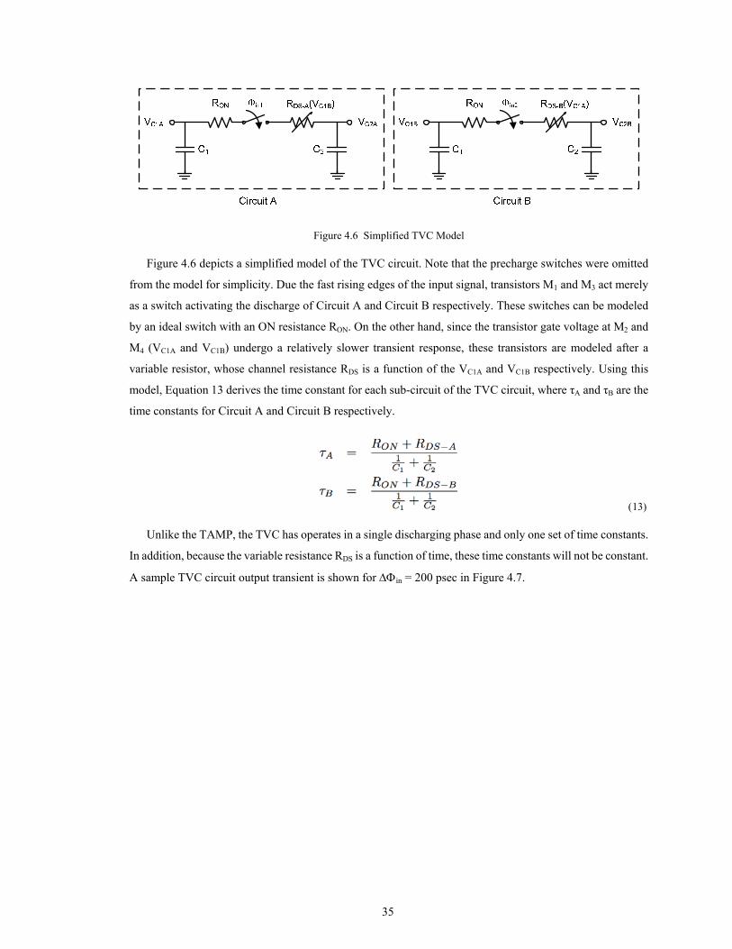
Figure 4.6 Simplified TVC Model
Figure 4.6 depicts a simplified model of the TVC circuit. Note that the precharge switches were omitted
from the model for simplicity. Due the fast rising edges of the input signal, transistors M1 and M3 act merely
as a switch activating the discharge of Circuit A and Circuit B respectively. These switches can be modeled
by an ideal switch with an ON resistance RON. On the other hand, since the transistor gate voltage at M2 and
M4 (VC1A and VC1B) undergo a relatively slower transient response, these transistors are modeled after a
variable resistor, whose channel resistance RDS is a function of the VC1A and VC1B respectively. Using this
model, Equation 13 derives the time constant for each sub-circuit of the TVC circuit, where τA and τB are the
time constants for Circuit A and Circuit B respectively.
(13)
Unlike the TAMP, the TVC has operates in a single discharging phase and only one set of time constants.
In addition, because the variable resistance RDS is a function of time, these time constants will not be constant.
A sample TVC circuit output transient is shown for ΔΦin = 200 psec in Figure 4.7.
35

ΔVout
Figure 4.7 TAMP-based TVC Transient for ΔΦin = 200 psec (C1 = C2 = 4 pF, W = 80 μm, Tr = 250 psec)
A typical transfer curve for this TVC circuit is shown in Figure 4.8 and demonstrates the circuit’s ability
to maintain a fairly linear conversion behavior for relatively small time differences. For larger time
differences however, the transfer characteristic becomes non-linear and saturates demonstrating some range
limitations to the device.
0.05 0.1 0.15 0.2 0.25 0.3 0.35 0.4 0.45
0.05
0.1
0.15
0.2
0.25
0.3
Output Signal Power vs. φin
Δφin
[nsec]
Out
put P
ower
[VR
MS]
Figure 4.8 –TAMP-base TVC Transfer Curve (C1 = C2 = 1 pF, W = 80 μm, Tr = 250 psec)
36

4.4 TVC Behavioral Characterization
Similar to the TAMP-based TDC architecture, the central block in the TVC-based TDC architecture is the
TVC circuit. Since the upper bound on overall performance of any TDC architecture is directly linked to the
characteristics of the front-end block, the design of the TVC circuit will have a direct impact on the
TVC-based TDC’s performance. There are in fact 3 main modifiable parameters in the TVC circuit:
capacitors C1 and C2, and transistor width W. A study on the effects of each parameter will be described in
this chapter.
To properly illustrate the impact of the different circuit parameters on the TVC’s performance, output
signal, distortion and noise were chosen as the main signals of interest for this analysis. In order to perform a
proper SNDR test, a sinusoidal input signal must first be generated. Since the input signal to a TVC circuit is
of the time-domain, a sinusoidal phase modulated clock must be generated as the one illustrated in Figure 4.9.
Φin2
Φin1
1/Ff
1/Fs
1/FΦ
Figure 4.9 – Sinusoidal Phase Modulated Clock Input
A critical concept for fast and accurate DSP-based testing is the notion of coherence. Coherence is
achieved when a waveform is sampled in such a way that the last sample of the first iteration wraps around
smoothly with the first sample of the second iteration. A coherent signal is a signal which has its frequency as
an integer multiple of the fundamental frequency Ff, also known as the frequency resolution. The coherent
frequency can be found with the following relationship where FS is the sampling frequency, N is the number
of samples collected at the sampling rate and M is an integer whose value ranges from 0 to N/2.
37

NFMMFF S
fC == (14)
M is also referred to as the Fourier spectral bin number and it refers to the number of cycles of the signal
completed in N samples. When choosing a value for M, it is important that both M & N are mutually prime,
that is, both numbers do not contain any common factor. The consequence of a non-mutually prime spectral
bin M is the introduction of quantization noise in a coherent signal in the form of periodic errors instead of a
randomly distributed error over the unit test period (UTP). Furthermore non-mutually prime spectral bins will
hit fewer code levels on the DAC and ADC because the same points will be tested repeatedly. This repetition
in testing leads to less robust fault coverage for both the DAC and ADC circuits. Note that careless selection
of spectral bins can lead to misleading results, thus, the importance of proper spectral bin selection.
In the following sections, transient simulations were performed for ΔΦin ranging from 0 to 500 psec in
steps of 10 psec. For each input value, the following parameters were selected: FΦ = 50 MHz, Fs = 50 MHz,
M = 101 and N = 210. The differential output voltage ΔVout was chosen to be sampled at 5 nsec from the rising
edge of Φin1. Then a 1024-point FFT was performed on the sampled data to plot the SNDR plots.
4.4.1 Capacitor C1 = C2 Sweep
The TVC circuit’s operation is mainly based on the transfer of charge from capacitors C1 to C2, therefore,
the choice of capacitor will have a significant impact on the transfer characteristic of the TVC circuit.
Keeping both capacitors C1 and C2 identical, a signal, distortion and noise plots from various capacitor
values, ranging from 1 pF to 4 pF are shown in Figure 4.10. A SNDR plot for the same capacitor sweep is
shown in Figure 4.11. Note that in the SNDR plot, the input magnitude is normalized with respect to 1 nsec.
From the output signal transfer curve, a clear relationship can be seen between the capacitor value and the
allowable input range. To understand this relationship, let us consider circuit behavior for both relatively
small and large ΔΦin.
38

0.05 0.1 0.15 0.2 0.25 0.3 0.35 0.4 0.45 0.5
0.05
0.1
0.15
0.2
0.25
0.3
0.35
Output Signal Power vs. φin
Δφin
[nsec]
Out
put P
ower
[VR
MS]
C
1=C
2=1pF
C1=C
2=2pF
C1=C
2=3pF
C1=C
2=4pF
0.05 0.1 0.15 0.2 0.25 0.3 0.35 0.4 0.45 0.5
0.01
0.02
0.03
0.04
0.05
0.06
0.07
0.08
0.09
Output Distortion Power vs. φin
Δφin
[nsec]
Out
put D
isto
rtio
n P
ower
[VR
MS]
C
1=C
2=1pF
C1=C
2=2pF
C1=C
2=3pF
C1=C
2=4pF
0.05 0.1 0.15 0.2 0.25 0.3 0.35 0.4 0.45 0.5
0.005
0.01
0.015
0.02
0.025
0.03
0.035
0.04
Output Noise Power vs. φin
Δφin
[nsec]
Out
put N
oise
Pow
er [V
RM
S]
C
1=C
2=1pF
C1=C
2=2pF
C1=C
2=3pF
C1=C
2=4pF
Figure 4.10 – TAMP-Based TVC Differential Voltage Signal, Distortion and Noise Plots for Capacitor C1 = C2 Sweep (W = 80 μm, Tr = 250 psec)
39

−40 −35 −30 −25 −20 −15 −10
10
20
30
40
50
60
SNDR Plot for C1=C
2 Sweep
Normalized Input Signal Magnitude Δφin
[dB]
Out
put P
ower
[dB
]
C
1=C
2=1pF
C1=C
2=2pF
C1=C
2=3pF
C1=C
2=4pF
Figure 4.11 – TAMP-Based TVC SNDR Plot for Capacitor C1 = C2 Sweep (W = 80 μm, Tr = 250 psec)
For small ΔΦin, Circuit A and Circuit B start discharging its capacitors at the arrival of Φin1 and Φin2
respectively. During this process, the cross-coupled nature of the TVC slowly increases the resistance in both
M2 and M4 just as in the TAMP OTA circuit. The larger the input time difference ΔΦin, the larger will be
difference between these transistor resistances and this will increase the voltage difference between VC2A and
VC2B. Once the gate-source voltage of transistor both M2 and M4 fall below the transistor threshold voltage Vt,
these transistors will enter cutoff and the output voltage ΔVout can be sampled. Note that for the case where
both capacitors C1 and C2 are identical, both Circuit A and Circuit B will stop discharging simultaneously. To
show this, let us first define the total initial charge Qtot stored on capacitor C1 as
(15)
Once the charge transfer has been initiated, by conservation of charge,
(16)
And since C1 and C2 are identical, we find the following relationship
(17)
And similarly,
(18)
Circuit A continues discharging until transistor M2 falls into cutoff.
40

(19)
Equation 19 indicates that both VGS2 and VGS4 are equivalent, thereby proving that both Circuit A and
Circuit B shut off simultaneously.
For large ΔΦin, that is an input time difference beyond the allowable input range of the TVC, Circuit A
will discharge and reach steady-state prior to the arrival of Φin2. The steady-state equilibrium voltage Veq can
be determined by the supply voltage and capacitors C1 and C2 from the following expression
(20)
In this particular example, Veq will be half the supply voltage. Once Circuit A has reached steady-state,
VC1A will reach Veq and determine the steady-state voltage VC2B to be measured in Circuit B.
(21)
Therefore, for large ΔΦin outside of the input dynamic range, the output voltage will saturate near the
threshold voltage Vt as shown below. This in fact corresponds to the upper limit ΔVout-max found in the output
signal transfer curve in Figure 4.10.
(22)
The effects of small and large ΔΦin on the TVC output transient curve are illustrated in Figure 4.12.
41

Figure 4.12 – Effects of Small and Large ΔΦin on TVC Transient Output
Note that ΔVout-max = Vt sets the maximum output dynamic range and is technology dependent. The input
dynamic range, however, is variable and controlled by the gain-conversion factor γ, which is a function of the
TVC parameters. The output signal transfer curve in Figure 4.10 shows that for smaller capacitances, the
TVC has larger gain γ and smaller linear input range. Note that this behavior is opposite to that of the TAMP
circuit described in chapter 3.6.1. This is attributed to the fact that the TAMP relies on the time constants in
Phase II to amplify the input time difference, whereas in the TVC, there is only a single phase of operation
determined by the time constants in Equation 13. The smaller capacitances lend to smaller time constants,
which accelerates the discharging process in Circuit A allowing it to saturate sooner. The opposite is also true
in that larger capacitances allow for longer discharging times for both sub-circuits, generating smaller output
voltage differences. The noise and distortion plots in Figure 4.10 indicates that an increase in capacitance
values reduces both noise and distortion components.
The SNDR plot in Figure 4.11 shows a decreasing SNDR for various capacitance values. This descending
trend indicates that the operational nature of the TVC is a non-linear process. The basic operation behind the
TVC circuit is that of a charge redistribution process between two capacitors, which is in itself considered
non-linear. Furthermore, the transistors M2 and M4 serve as variable resistors to control the current flow in the
charge transfer. The changing nature of both VGS and VDS in these transistors lend to highly non-linear
resistances. Despite of the TVC’s inherent non-linearity, the TVC circuit can still be operated considered
linear within a certain degree of resolution. For example, if an application requires a resolution of 8-bits, the
allowable linear input dynamic range for this application should be such that the SNDR is above
approximately 48 dB. This translates to an allowable input range from -40dB to -22dB for a 8-bit resolution.
Thus, there is a trade-off relationship between resolution and input dynamic range of the TVC. While, the
maximum allowable input is set by the minimum resolution requirement of an application, the minimum
allowable input is determined by the smallest detectable voltage by the following ADC in the TVC-base TDC
architecture. The SNDR plot also suggests the presence of an optimal capacitance value for peak SNDR
performance.
42

4.4.2 Capacitor C2/C1 Sweep
Just like the TAMP, the TVC can also break capacitor symmetry to provide gain benefits. By varying the
ratio between capacitors C1 and C2, larger gain-conversion factors can be achieved at the expense of reduced
input dynamic range. This result comes at no surprise since the TVC was initially derived from the TAMP
structure. Increasing C2 with respect to C1 results in a faster discharging of C1 compared to C2 as fewer
charges are required to vary the same voltage on a smaller capacitor than on a larger capacitor. With VC1A and
VC1B being cross-coupled to M2 and M4, a larger channel resistance minimizes the charge redistribution
process on one of the sub-circuits and results in a larger differential output voltage. A plot of the effects of
capacitor ratio on the TVC output signal, distortion and noise components are shown in Figure 4.13.
A SNDR plot for the same capacitor ratio sweep is shown in Figure 4.14. Observe that larger C2/C1 ratio
increases SNDR at the expense of a smaller input dynamic range. This can be explained by the fact that by
increasing C2 with respect to C1, although the time constants are increased, VC1A and VC1B experience a faster
change in voltage. This in turn causes the resistances in the cross-coupled transistors M2 and M4 to have a
sharper change from low to high impedance. Thus, the fast changing gate voltages causes these transistors to
behave more like a switch and therefore minimizes the distortion errors introduced by the non-linear
resistance characteristic of the MOS transistor, increasing the overall SNDR of the circuit.
43

0.05 0.1 0.15 0.2 0.25 0.3 0.35 0.4 0.45 0.5
0.05
0.1
0.15
0.2
0.25
0.3
0.35
Output Signal Power vs. φin
for C1 = 1pF
Δφin
[nsec]
Out
put P
ower
[VR
MS]
C2/C
1=0.50
C2/C
1=1
C2/C
1=1.50
C2/C
1=2
0.05 0.1 0.15 0.2 0.25 0.3 0.35 0.4 0.45 0.5
0.02
0.04
0.06
0.08
0.1
Output Distortion Power vs. φin
for C1 = 1pF
Δφin
[nsec]
Out
put D
isto
rtio
n P
ower
[VR
MS]
C2/C
1=0.50
C2/C
1=1
C2/C
1=1.50
C2/C
1=2
0.05 0.1 0.15 0.2 0.25 0.3 0.35 0.4 0.45 0.5
0.01
0.02
0.03
0.04
0.05
0.06
0.07
0.08
0.09
Output Noise Power vs. φin
for C1 = 1pF
Δφin
[nsec]
Out
put N
oise
Pow
er [V
RM
S]
C
2/C
1=0.50
C2/C
1=1
C2/C
1=1.50
C2/C
1=2
Figure 4.13 – TAMP-Based TVC Differential Voltage Signal, Distortion and Noise Plots for Capacitor C2/C1 Sweep (C1 = 1 pF, W = 80 μm, Tr = 250 psec)
44

−40 −35 −30 −25 −20 −15 −10
10
20
30
40
50
60
SNDR Plot for C2/C
1 Ratio Sweep
Normalized Input Signal Magnitude Δφin
[dB]
Out
put P
ower
[dB
]
C
2/C
1=0.50
C2/C
1=1
C2/C
1=1.50
C2/C
1=2
Figure 4.14 – TAMP-Based TVC SNDR Plot for Capacitor C2/C1 Sweep (C1 = 1 pF, W = 80 μm, Tr = 250 psec)
4.4.3 Transistor Width W Sweep
Figure 4.15 shows a plot of the effects of transistor width W on the TVC output signal, distortion and
noise components. Note that in this particular sweep, all transistors were kept the same size as to conserve
symmetry. The result of larger transistor sizes on the TVC performance is a higher gain-conversion factor.
Because of the inverse relation between transistor size and resistance, larger sizes result in smaller
resistances, which reduce the average time constant of the system. This effect is similar to that seen in the
TAMP. Also, due to restrictions on the maximum output voltage in the TAMP-based TVC, a larger gain
translates to an earlier saturation point, hence reducing the allowable input range.
The SNDR plot in Figure 4.16 indicates that larger transistor widths can contribute to higher SNDR by
causing fast switching of M2 and M4 and reducing distortion errors from the MOS resistance. Note also that
while smaller transistor widths lower the peak SNDR of the circuit, the input dynamic range is extended due
to a delayed output saturation point, which pushes distortion components to larger inputs.
45

0.05 0.1 0.15 0.2 0.25 0.3 0.35 0.4 0.45 0.5
0.05
0.1
0.15
0.2
0.25
0.3
0.35
Output Signal Power vs. φin
for C1 = C
2 = 2.8pF
Δφin
[nsec]
Out
put P
ower
[VR
MS]
0.05 0.1 0.15 0.2 0.25 0.3 0.35 0.4 0.45 0.5
0.01
0.02
0.03
0.04
0.05
0.06
0.07
Output Distortion Power vs. φin
for C1 = C
2 = 2.8pF
Δφin
[nsec]
Out
put D
isto
rtio
n P
ower
[VR
MS]
0.05 0.1 0.15 0.2 0.25 0.3 0.35 0.4 0.45 0.5
2
4
6
8
10
12
14
16
x 10−3 Output Noise Power vs. φ
in for C
1 = C
2 = 2.8pF
Δφin
[nsec]
Out
put N
oise
Pow
er [V
RM
S]
W = 20μmW = 40μmW = 60μmW = 80μm
W = 20μmW = 40μmW = 60μmW = 80μm
W = 20μmW = 40μmW = 60μmW = 80μm
Figure 4.15 – TAMP-Based TVC Differential Voltage Signal, Distortion and Noise Plots for Transistor Width W Sweep (C1 = C2 = 2.8 pF, Tr = 250 psec)
46

−40 −35 −30 −25 −20 −15 −10
15
20
25
30
35
40
45
50
55
60
65
SNDR Plot for W Sweep
Normalized Input Signal Magnitude Δφin
[dB]
Out
put P
ower
[dB
]
W = 20μmW = 40μmW = 60μmW = 80μm
Figure 4.16 – TAMP-Based TVC SNDR Plot for Transistor Width W Sweep (C1 = C2 = 2.8 pF, Tr = 250 psec)
4.5 Summary
This chapter introduces a new TVC-based TDC architecture which improves on the TAMP-based TDC’s
shortcomings. The derivation of the new TVC circuit evolved from the TAMP was also presented. In
addition, the TVC’s transfer characteristics were simulated for different capacitor combinations, clearly
illustrating the resolution vs. input range trade-off. The SNDR plots were then plotted to illustrate the TVC’s
mode of operation in the non-linear region.
47
Chapter 5
Experimental Results
5.1 Introduction
In order to provide proof of concept for the TVC-based TDC, a working TVC prototype circuit is built
from discrete components. This chapter presents some TVC design considerations as well as a detailed
implementation of the TVC test bench. Experimental measurements for various TVC configurations are then
shown to confirm simulation results.
5.2 Discrete TVC Design
The TVC circuit was implemented on a V1224 Vector prototype board using discrete MOS transistor
components. STMicroelecetronics 2N7000 NMOS and Zetex ZVP3306A PMOS transistors were used in the
implementation of the prototype circuit. Special care was taken into keeping straight connections and
minimizing wire length to minimize inductance. Moreover, careful consideration was given to component
layout and wire placements to minimize inductance loop. Since the TVC circuit’s output voltage range is
dependent on the threshold voltage Vt, the supply voltage is increased to 5 V to accommodate for the larger
threshold associated with discrete MOS components. The complete circuit diagram and picture are shown
in Figure 5.1 and Figure 5.2. Note that dummy switches were added to the original reset circuitry of the TVC
circuit to reduce the effects of charge injection during switching. These additional switches absorb any
residual charges left from the channel of the precharging transistors during switch off that would have
otherwise gone onto the capacitors. This in effect ensures that the TVC capacitors are properly charged and
discharged to their correct values.
48

Figure 5.1 – Discrete TVC Circuit Schematic
Precharge Network
Figure 5.2 – Discrete TVC Circuit on Vector Prototype Board
5.3 Experiment Setup
In order to fully describe the discrete TVC’s transfer characteristic behavior, the TVC’s differential
output results need to be collected for varying degree of phase inputs. The input phase differences are
generated using an Agilent 81130A Pulse/Pattern Generator. This device can generate four clock sources:
two independent clock sources Φin1 and Φin2, whose phase can be accurately controlled, and their
complements. The experimental test bench was set up to collect repeated voltage measurements for a
specified phase input ∆Φin. The full experimental setup of the TVC circuit can be seen in Figure 5.3
and Figure 5.4.
Main TVC Circuit
Line Driver
49

Figure 5.3 – TVC Test Bench Schematic
Figure 5.4 – TVC Test Bench Setup
50

In order to design the test bench to collect multiple time-to-voltage measurements, a set of reset signals
are generated between measurements to reinitialize the TVC circuit. As shown from the full timing diagram
of the TVC test bench signals in Figure 5.5, the TVC differential output voltage ∆Vout is sampled at a constant
time interval and followed by a reset clock signals. It is important not to have an independent clock source for
the reset clocks, since the slightest mismatch in frequency between Φin1 and the reset clocks can cause the
clocks to shift relative to each other. Therefore, it is necessary for the reset clocks to be synchronized with
Φin1 using a PLL with a phase delay as shown in Figure 6.1. This configuration is only valid assuming that the
Φin1 remains the leading input phase and remains periodic.
Figure 5.5 TVC Test Bench Timing Diagram
However, in the case of aperiodic inputs, the reset pulse must also be aperiodic and thus, it can be
generated by delaying the leading input phase through a chain of delay cells as shown in Figure 6.2. In this
thesis, the latter was used as it proved both effective for periodic and aperiodic inputs.
Since the reset clock constitutes no more than a delayed version of the leading input Φin1, the reset signals
are generated using a set of counters and comparators programmed through an Altera Stratix DSP
development board. Although Φin1 could have been tapped to generate its delayed version, to avoid a loading
mismatch, the complement of Φin1 was used instead because of its availability from the Agilent 81130A
Pulse/Pattern Generator. Figure 5.6 shows the programmed FPGA logic block diagram. Note that the FPGA
uses its internal 80 MHz crystal oscillator as a trigger for the counter blocks. The fact that this oscillator is
asynchronous from the external clocks has no significant effects on the operation of the TVC since the exact
placement of the reset signal need not be accurate as long as it occurs after the data has been sampled and
provides a long enough time for the precharge and discharge phases to complete.
51

Figure 5.6 FPGA Logic Block Diagram for Reset Clock Generation
Due to the 3.3 V supply voltage of the Altera Stratix DSP development board, the generated reset clocks
are limited to 3.3 V. Since the supply voltage on the discrete TVC circuit was set at 5 V, Texas Instruments
SN75112 Dual Line Drivers were used to drive the reset clocks to the supply rail. The results of the TVC
circuit are then sampled, collected and processed through an Agilent Infiniium 54830D Mixed-Signal
Oscilloscope.
5.4 Experimental Results
Measurements were taken by varying the input phase difference between the two sources of the Agilent
81130A Pulse/Pattern Generator pattern generator from 0 to 50 nsec in increments as little as 100 psec. The
frequency of both clocks was set to 400 kHz. While a higher input frequency would be theoretically possible
as long as it allows the TVC enough time to precharge to its initial condition, 400 kHz was chosen purely to
stay within the pattern generator’s band of operation. However at larger frequency ranges, ringing effects
were observed, which can cause significant signal degradation and non-linearities. Figure 5.7 shows the TVC
output transients (VC2A, VC2B and ∆Vout) sampled at 100 MHz with no averaging performed.
Due to the nature of discrete component circuit construction, there are larger noise contributions than
would be expected from an integrated design. This level of voltage noise can have a negative impact on
measurement repeatability and cannot be taken neglected. Large coupling capacitors were put to reduce
supply noise as well as short and flat wire paths along the prototype board to reduce inductance effects.
However, despite these precautions, noise contributions to the TVC output are still significant and proper
noise analysis must be conducted. A voltage histogram test can be performed at the output to measure the
average noise contributions. Figure 5.8 shows the histogram test at the TVC differential output voltage ∆Vout
for a sampling instant at 1.1 µsec from Φin1. The histogram reveals a Gaussian noise function with 96.3% of
the noise within 2σ. The mean of the Gaussian distribution represents the average output voltage measured
from the TVC and the standard deviation corresponds to the average noise value.
52

VC2A
VC2B
∆Vout
Figure 5.7 Oscilloscope Screen Capture of TVC Output with No Averaging (∆Φin=10nsec, C1=C2=2.2nF)
Figure 5.8 Noise Histogram for TVC Differential Output ∆Vout (∆Φin=10nsec, C1=C2=2.2nF)
To reduce the effects of output noise voltage of the TVC, a 4096-point running averaging was performed
by the oscilloscope. This averaging process effectively reduces the output noise by a factor of 64 as shown
from the following relationship
53

(23)
where N is the size of the sequence length and equal to 4096. Note that there is no sampling clock
necessary in our TVC test setup to collect the output differential voltage ∆Vout. The data is collected by
consistently logging the measured ∆Vout at a specific instant following the leading edge Φin1. In this thesis, all
experimental measurements were taken at a 1.1 µsec delay from the rising edge of Φin1, which is define as
being the sampling delay ts as is depicted in Figure 5.9.
∆V out
ts = 1.1 µsec
Figure 5.9 Oscilloscope Screen Capture of TVC Output with 4096-Point Running Average (∆Φin=10nsec, C1=C2=2.2nF)
From the transient response in the figure above, we observe that ∆Vout is relatively constant within the
period of interest and corresponds with earlier Cadence simulation results. The relatively stable nature of the
output suggests the TVC’s robustness to small deviations in sampling instants often seen from clock jitter.
5.5 Transfer Characteristic Testing
A transfer characteristic curve is drawn from the prototype TVC circuit with identical C1 and C2
capacitors of 2.2 nF. The resulting data for an input phase sweep from 0 to 50 nsec is shown in Figure 5.10.
As predicted from simulation results, the transfer curve adopts a small linear region before reaching
saturation near the transistor’s threshold voltage Vt. Thus the linear dynamic range of this TVC configuration
is approximately 500 mV, corresponding to an input range of 7 nsec. The gain is this region is found to be
71.4 mV/ns. The results also indicate the presence of an input offset of -97.51 mV. This can be attributed to
54

slight mismatches in capacitors between Circuit A and Circuit B of the TVC which causes uneven capaciotr
charging. Moreover, since the output voltage is directly related to the amount of charge transferred from C1 to
C2, mismatches in threshold voltage Vt can also cause differences in transconductance between transistors M2
and M4 leading to different steady-state voltages when the transistors reach cutoff. For the discrete
components used, Vt is documented as having large variations. Despite the sensitive nature of the TVC’s
sensitivity to Vt, for an CMOS implementation of the TVC, the effects resulting from such mismatches are
expected to be smaller due to tight CMOS process controls.
Figure 5.10 Discrete TAMP-Based TVC Transfer Curve for C1=C2=2.2nF
Other transfer curves were also measured for different capacitor configurations. A comparison of the
results is depicted in Figure 5.11. In accordance to TVC simulations, for a symmetrical C1 = C2 design, as the
capacitor values increase, there is a drop in gain-conversion factor γ attributed to the increase in the circuit’s
time constant. However, at the expense of a lower gain, this configuration increases its linear range. Varying
degree input offset mismatches between the different TVC configurations is observed and can be eliminated
through proper calibration techniques.
55

Figure 5.11 Discrete TAMP-Based TVC Transfer Curve Comparison
The gain of the TVC can be further improved by having an asymmetrical capacitor design. In accordance
to simulation results, the larger C2/C1 capacitor ratios, the gain-conversion factor can be increased at the
expense of a smaller dynamic range. In the case of a smaller ratio, the TVC can cover a wide range in input
time differences, but at the cost of a lower resolution. This clearly demonstrates the trade-off between
resolution and input dynamic range as observed in simulations.
5.6 DNL and INL Testing
Because the TVC converts analog time domain information into an analog voltage domain, much like any
converter, linearity tests, such as differential nonlinearity (DNL) and integral nonlinearity (INL), can be
performed. While DNL is a measurement of how consistent the step sizes are from one level to the next, INL
measures the accumulated errors in step size. For each of the different capacitor configurations, the input
range was chosen to cover the widest linear range on the TVC’s transfer curve. A best-fit DNL and INL test
were then performed on each configuration with a defined LSB time step of 100ps. It is important to note that
these plots do not bare the full quantitative meaning of traditional ADC or DAC DNL and INL testing, but
rather they serve to give a qualitative comparison in linearity between the different TVC circuit
configurations. The results from each of the tested TVC configuration will be analyzed in the following
sections. For the purpose of comparison between the different configurations, note that the analysis for the
TVC configuration (C1=5.6nF, C2=2.2nF) will not be shown due to the different LSB time step used during
56

measurement testing.
5.6.1 TAMP-Based TVC Configuration 1: C1 = C2 = 2.2 nF
A plot of the linear region of the TAMP-based TVC curve for C1 = C2 = 2.2 nF is shown in Figure 5.12.
The linear range extends from 0 nsec to 7 nsec. Its corresponding DNL and INL curves are shown in Figure
5.12 and Figure 5.13. The DNL error for this first configuration is found to be within ±0.45 LSB, keeping
fairly consistent step sizes. The INL curve shows a maximum absolute error of 0.79 LSB with respect to the
best-fit-line, which translates to an error of 79 psec.
0 1 2 3 4 5 6 7
−50
0
50
100
150
200
250
300
350
TVC Transfer Curve
Δφin
[nsec]
Δ V
out [m
V]
Figure 5.12 Discrete TAMP-Based TVC Linear Region and Best-Fit-Line (C1 = C2 = 2.2 nF)
57

0 1 2 3 4 5 6
−0.4
−0.3
−0.2
−0.1
0
0.1
DNL Curve for TVC
Δφin
[nsec]
DN
L [L
SB
]
Figure 5.13 DNL Curve within Linear Region of Discrete TAMP-Based TVC (C1 = C2 = 2.2 nF)
0 1 2 3 4 5 6 7
−0.6
−0.4
−0.2
0
0.2
0.4
0.6
INL Curve for TVC
Δφin
[nsec]
INL
[LS
B]
Figure 5.14 INL Curve within Linear Region of Discrete TAMP-Based TVC (C1 = C2 = 2.2 nF)
5.6.2 TAMP-Based TVC Configuration 2: C1 = C2 = 5.6 nF
A plot of the linear region of the TAMP-based TVC curve for C1 = C2 = 5.6 nF is shown in Figure 5.15.
Its linear range is larger than for the case of smaller capacitors due to a smaller gain-conversion factor. The
DNL curve in Figure 5.16 shows that the DNL error is within ±0.60 LSB, which is slightly higher than in the
previous configuration. The INL curve in Figure 5.17 indicates a peak INL error of 1.20 LSB. This error is
58

attributed to the initial offset error. However, excluding this first error, the remainder of the INL error is well
within ±1 LSB.
0 5 10 15
−200
−100
0
100
200
300TVC Transfer Curve
Δφin
[nsec]
Δ V
out [m
V]
Figure 5.15 Discrete TAMP-Based TVC Linear Region and Best-Fit-Line (C1 = C2 = 5.6 nF)
0 2 4 6 8 10 12 14
−0.5
−0.4
−0.3
−0.2
−0.1
0
0.1
0.2
0.3
0.4
0.5
DNL Curve for TVC
Δφin
[nsec]
DN
L [L
SB
]
Figure 5.16 DNL Curve within Linear Region of Discrete TAMP-Based TVC (C1 = C2 = 5.6 nF)
59

0 5 10 15
−0.6
−0.4
−0.2
0
0.2
0.4
0.6
0.8
1
1.2INL Curve for TVC
Δφin
[nsec]
INL
[LS
B]
Figure 5.17 INL Curve within Linear Region of Discrete TAMP-Based TVC (C1 = C2 = 5.6 nF)
5.6.3 TAMP-Based TVC Configuration 2: C1 = 2.2 nF, C2 = 5.6 nF
For the case of a non-uniform capacitor configuration (C1 = 2.2 nF, C2 = 5.6 nF), the linear transfer curve
from 0 nesc to 5 nsec is plotted in Figure 5.18. Contrary to the previous case, the larger gain obtained from
this configuration severely limits the linear input dynamic range of the circuit. The DNL and INL curves
in Figure 5.19 and Figure 5.20 show a DNL error within ±0.45 LSB and an INL error within ±1.16 LSB. Like
in the previous case, the large INL error stems mainly from the initial offset voltage. In addition,
measurements indicate signs of large upward and downward bends in the INL curve due to monotonically
increasing and decreasing DNL errors which may cause failure in INL requirements.
60

0 1 2 3 4 5
−300
−200
−100
0
100
200
300
400
500
TVC Transfer Curve
Δφin
[nsec]
Δ V
out [m
V]
Figure 5.18 Discrete TAMP-Based TVC Linear Region and Best-Fit-Line (C1 = 2.2 nF, C2 = 5.6 nF)
0 1 2 3 4
−0.4
−0.3
−0.2
−0.1
0
0.1
0.2
DNL Curve for TVC
Δφin
[nsec]
DN
L [L
SB
]
Figure 5.19 DNL Curve within Linear Region of Discrete TAMP-Based TVC (C1 = 2.2 nF, C2 = 5.6 nF)
61

0 1 2 3 4 5−0.8
−0.6
−0.4
−0.2
0
0.2
0.4
0.6
0.8
1
INL Curve for TVC
Δφin
[nsec]
INL
[LS
B]
Figure 5.20 INL Curve within Linear Region of Discrete TAMP-Based TVC (C1 = 2.2 nF, C2 = 5.6 nF)
5.6.4 INL and DNL Summary
The DNL tests show that all designs experience a DNL error within ±0.60 LSB. However, the INL curve
shows an absolute INL error of approximately 1.20 LSB, most of which stems from large offset errors. These
errors may be considered too large for certain applications requiring very-fine time resolution. For reasonably
good TDC applications, the DNL error should typically be within ±0.25 LSB and the INL error, within ±0.5
LSB. Therefore, for the specified linear range for the different TVC configurations fail to meet these
requirements. However, by selecting a larger LSB size, the TVC may improve linearity errors while
sacrificing resolution. Moreover, note that discrete components were used for the construction of the TVC
circuit, which exposes the circuit to significant noise and ideally, an IC implementation should deem better
results. The INL curves also indicate that the TVC circuit can be configured to cover different ranges of
interest at different resolutions by selecting different capacitor combinations while still maintaining adequate
linearity. A summary of the results from the different TVC configurations is found in Table 5.1.
62

Table 5.1 TAMP-Based TVC Configurations Summary (LSB = 100 psec)
C1 = 2.2nF, C2 = 5.6nF C1 = 2.2nF, C2 = 2.2nF C1 = 5.6nF, C2 = 5.6nF C1 = 5.6nF, C2 = 2.2nF
Input Dynamic Range
0 to 5 nsec 0 to 7 nsec 0 to 15 nsec 0 to 40nsec
Output Dynamic Range
‐321.61 mV to 583.06 mV
‐97.51 mV to 395.37 mV
‐263.04 mV to 302.25 mV
‐139.09 mV to 49.33 mV
BestFitLine Gain γ 18.84 mV/nsec 70.94 mV/nsec 38.05 mV/nsec 484.24 mV/nsec
BestFitLine Offset ‐343.45 mV ‐96.78 mV ‐267.62 mV ‐138.00 mV
Average |INL| 0.36 LSB 0.31 LSB 0.34 LSB N/A
Maximum |INL| 1.16 LSB 0.79 LSB 1.20 LSB N/A
Average |DNL| 0.11 LSB 0.10 LSB 0.15 LSB N/A
Maximum |DNL| 0.45 LSB 0.45 LSB 0.60 LSB N/A
Average Noise 8.80 mV 12.04 mV 9.54 mV 8.71 mV
5.7 Summary
This chapter discussed the implementation of a discrete TVC circuit using a Vector prototype board.
Experimental measurements reveal significant noise contributions to the differential output, which is
mitigated through a 4096-point average. In addition, the TVC design offers a flexible solution for different
range and resolution requirements via different capacitor combinations. Also, the prototype circuit shows
good linearity within a relatively small range of interest.
63

Chapter 6
Conclusions and Future Research
6.1 Conclusions
Time-domain testing remains one of the most challenging obstacles for the semiconductor industry in
mixed-signals testing. With increasing size and complexity of high-performance CMOS ICs, conventional
production testers are inadequate for today’s high-precision time measurement requirements as most timing
quantities to be measured are often of the same order of magnitude as the timing resolution of stand-alone
measurement devices. To mitigate the problem, distance between the tester and the DUT can be minimized
and a custom time measurement device like the TDC can be developed and implemented along side the DUT
on a single chip. However, traditional high-resolution TDC architectures suffer from long dead times and
preventing it to be used in real-time applications.
In this work, a study of the TAMP circuit for high-resolution TDC application is presented. Modification
were made to the original TAMP and simulation results in 0.18µm-CMOS technology were shown to observe
the effects of various circuit parameters on performance. Some design challenges were also discussed and
used to motivate the development of a new TDC using a TAMP-based Time-to-Voltage Converter (TVC),
which provide shorter dead times than most conventional TDC architectures. SNDR simulations were
performed and used to demonstrate the TVC’s high-resolution capability despite its non-linear operational
behavior and limited dynamic input range. Experimental results from a discrete implementation of the TVC
are then discussed to confirm good linearity over a relatively small range of interest as well as the effects of
various capacitor configurations on circuit performance.
64

6.2 Future Research
In this section, future research topics are suggested to extend the TVC concept and demonstrate its
performance in production testing applications. Further work is also outlined to improve on the TAMP-based
TVC linearity and gain-conversion factor.
6.2.1 IC Implementation
In order to further demonstrate the TAMP-based TVC in TDC applications, an IC chip can be fabricated
in 0.18µm-CMOS process. Note that during experimental results, the sampling was performed automatically
by the oscilloscope. Therefore, for on-chip fabrication, a sampling switch needs to be added at the output of
the TVC controlled by a sampling clock. As mentioned in Chapter 5.3, the sampling clock can be generated
from Φin1 using a PLL block or a delay cell. However, note that the addition of either of these structures to the
input of Φin1 leads to asymmetric loading effects to be experienced between inputs Φin1 and Φin2. This in turn
can cause uneven delay between the input phases and variations in rise and fall times Tr, which add to phase
errors. The problem of mismatched loading can be mitigated by using dummy PLLs or delay chains to load
the input of Φin2. Note also that Special care should also be taken in transistor and capacitor matching between
Circuit A and Circuit B of the TVC structure by employing a common centroid layout.
Φin1
Φin2
Dummy PLL
Reset
VC2A
VC2B
Figure 6.1 Generation of TVC Reset Clock for Periodic Inputs with Even-Matching
65

Figure 6.2 Generation of TVC Reset Clock for Aperiodic Inputs with Even-Matching
6.2.2 Calibration
Although the TAMP-based TVC presented in this thesis retains a relatively linear behavior from
time-domain conversion to voltage domain, the relatively short input range prevents this circuit from being
used in many applications where resolution and wide range is required. A possible solution to extend the
dynamic range is through the use of linearization techniques seen in many ADC. The first is to provide an
off-line calibration technique where the non-linear data is stored in digital memory and used as a look-up
table to establish a mapping between the original input and its ideal output [24]. However, this method cannot
take into account variations due to ageing and temperature drifts. Thus, an on-line solution should be
developed through a feedback loop to ensure constant calibration.
6.2.3 Asymmetrical TVC Design
The TAMP-based TVC could be further modified to exhibit larger gains-conversion factors by combining
two asymmetric TVCs with appropriate data selection depending on the order of the input edge arrivals. By
breaking the symmetry in each TVC sub-circuit, more specifically by varying the capacitor combination
between the two sub-circuits as shown in Figure 6.3, the charging rates can be manipulated to generate larger
output voltage differences and achieve larger TVC gains. Note that since the symmetry is broken between the
two sub-circuits, the TAMP can no longer accommodate for both positive and negative ΔΦin. Therefore an
arbiter is necessary to determine the polarity of ΔΦin and select the appropriate result from the two
asymmetric TVC circuits as shown in Figure 6.4.
66

C1 C2
VC2A
Φin1
VC1A
VC1B
Reset
Reset
Precharge Switch
Precharge Switch
C3 C4
VC2B
Φin2
VC1B
VC1A
Reset
Reset
Precharge Switch
Precharge Switch
M2M1 M4M3
Circuit A Circuit B Figure 6.3 Asymmetrical TAMP-based TVC Circuit
MUX
Arbiter
ΔVout1
ΔVout2
TVC1
TVC2
Φin1
Φin2
ΔVout
Figure 6.4 Asymmetrical TVC Architecture with Arbiter Data Selection
67
References
[1] S. Y. Yurish, “Sensors and transducers: Frequency output versus voltage output,” Sensors & Transducers Magazine, vol. 49, no. 11, pp. 302–305, Nov. 2004.
[2] E. Räisänen-Ruotsalainen, T. Rahkonen, and J. Kostamovaara, “An integrated time-to-digital converter with 30-ps single-shot precision,” in IEEE J. Solid-State Circuits, vol. 35, no. 10, pp. 1507–1510, Oct. 2000.
[3] K. Määttä and J. Kostamovaara, “A high-precision time-to-digital converter for pulsed time-of-flight laser radar applications,” in IEEE Trans. on Instrum. Meas., vol. 47, no. 2, pp. 521–536, Apr. 1998.
[4] V. Ramakrishnan and P. T. Balsara, “A wise-range, high-resolution, compact, CMOS time to digital conveter,” in Proc. Int. Conf. VLSI Design (VLSID’06), Jan. 2006.
[5] T. Otsuji, “A picosecond-accuracy 700-MHz range Si-polar time interval counter LSI,” IEEE J. Solid-State Circuits, vol. 28, pp. 941–947, Sept. 1993.
[6] T. Rahkonen, E. Malo, and J. Kostamovaara, “A 3-V fully integrated digital FM demodulator based on a CMOS pulse-shrinking delay line,” in Proc. IEEE Int. Symp. Circuits and Systems (ISCAS’96), vol. 2, pp. 572–575, May 1996.
[7] T. Xia and J. C. Lo, “Time-to-voltage converter for on-chip jitter measurement,” in IEEE Trans. on Instrum. Meas., vol. 52, no. 6, pp. 1738–1748, Dec. 2003.
[8] “International Technology Roadmap for Semiconductors,” [Online]. Available: http://www.itrs.net/Common/2005ITRS/Home2005.htm, 2005.
[9] M. Oulmane and G. W. Roberts, “A CMOS time amplifier for femto-second resolution timing measurement,” in Proc. IEEE Int. Symp. Circuits and Systems (ISCAS’04), vol. 1, pp. 509–512, May 2004.
[10] A.M. Abas, A. Bystrov, D.J. Kinniment, O.V. Maevsky, G. Russell and A.V. Yakovlev, “Time difference amplifier,” Electronic Letters, vol. 38, no. 23, pp. 1437–1438, Nov. 2002.
[11] V. Gutnik and A. Chandrakasan, “On-chip picosecond time measurement,” in Symp. On VLSI Circuits, pp. 52–53, June 2000.
[12] S. Tisa, A. Lotito, A. Giudice, and F. Zappa, “Monolithic time-to-digital converter with 20ps resolution,” in Proc. European Solid-State Circuits Conf., pp. 465–468, Sept. 2003.
68

69
[13] P. Chen, S.-I. Liu, and J. Wu, “A CMOS pulse-shrinking delay element for time interval measurement,” in IEEE Trans. on Circuits and Systems, pp. 954–958, Sept. 2000.
[14] C.-C. Chen, P. Chen, C.-S. Hwang, and W. Chang, “A Precise Cyclic CMOS Time-to-Digital Converter With Low Thermal Sensitivity,” in IEEE Trans. on Nuclear Science, vol. 52, no. 4, pp. 834–838, Aug. 2005.
[15] P. Levine, “High-Resolution Time Measurement and Calibration for On-Chip Test Systems,” M.Eng. thesis, McGill University, Montreal, Qc., Canada, July 2004.
[16] P. Chen, C.-C. Chen, J.-C. Zheng, and Y.-S. Shen, “A PVT Insensitive Vernier-Based Time-to-Digital Converter With Extended Input Range and High Accuracy,” in IEEE Trans. on Nuclear Science, vol. 54, no. 2, pp. 294–302, Apr. 2007.
[17] P. M. Levine and G. W. Roberts, “A high-resolution flash time-to-digital converter and calibration scheme,” in Proc. Int. Test Conf. (ITC’04), pp. 1148–1157, Oct. 2004.
[18] P. Dudek, S. Szczepański, and J. Hatfeld, “A high-resolution CMOS time-to-digital converter utilizing a Vernier delay line," IEEE J. Solid-State Circuits, vol. 35, no. 2, pp. 240–247, Feb. 2000.
[19] R. H. Walden, “Analog-to-digital converter survey and analysis," IEEE J. Selected Areas in Communications, vol. 17, no. 4, pp. 539550, Apr. 1999.
[20] M. Burns, G. W. Roberts, An Introduction to Mixed-Signal IC test and Measurement, New York: Oxford University Press, 2001.
[21] J. A. Gasbarro and M. A. Horowitz, “Integrated pin electronics for VLSI functional testers," IEEE J. Solid-State Circuits, vol. 24, no. 2, pp. 331337, Apr. 1989.
[22] A. H. Chan and G. W. Roberts, “A jitter characterization system using a component-invariant Vernier delay line," in IEEE Trans. on Very Large Scale Integration (VLSI) Systems, vol. 12, no. 1, pp. 7995, Jan. 2004.
[23] M. Hafed, N. Abaskharoun, and G. W. Roberts, “A stand-alone integrated test core for time and frequency domain measurements,” in Proc. Int. Test Conference, pp. 1031–1040, Oct. 2000.
[24] U. Gatti, G. Gazzoli, F. Maloberti, “Improving the linearity in high-speed analog-to-digital converters,” in Proc. IEEE Int. Symp. Circuits and Systems (ISCAS’98), vol. 1, pp. 17–20, June 1998.