A Study of Folding and Interpolating ADC - Idea2IC.html€¦ · 1 A Study of Folding and...
7
1 A Study of Folding and Interpolating ADC Yun Chiu and Dejan Marković Abstract–An architectural exploration and analysis of performance limitations in folding/interpolation analog-to- digital converters (ADCs) is presented. The analysis is based on a behavioral MATLAB/SIMULINK model, which captures non- idealities such as mismatch and non-linearity in the folding amplifiers, interpolation network and comparators. The focus of the study has been placed on the design trade-offs in direct and cascaded folding architectures in CMOS operating at low supply voltages. We propose the differential folding and an efficient radix-5, 2-stage cascaded architecture. In addition, we propose a novel bit alignment scheme that can be used for the cascaded folding structure, which greatly reduces the total number of comparators, which is only 5+5+12=22 for an 8-bit prototype. Monte-Carlo simulation is performed and results are summarized. I. INTRODUCTION With the rapid expansion of broadband digital communication over the past two decades, medium and low- resolution analog-to-digital converters (ADCs) attract a lot of attentions as one of the most important building blocks for the analog front-end. Flash and folding/interpolating architectures stand as the main choices due to their amenability to the continuous device scaling of the digital CMOS process. Compared to the flash architecture, where the hardware complexity is proportional to 2 n (n is the resolution bits), the use of folding reduces the number of comparators by 2 m (m is the folding factor). Comparator number reduction stems from the fact that each comparator is used more than once. In addition to folding, interpolation further reduces the number of preamps required for the fine quantizer. This converter inherits the one-step nature of the flash converter yet greatly reduces the hardware complexity. Therefore it is generally believed to be a smart replacement of the flash architecture. This report is organized as follows. In section 2 we present direct and cascaded ADC architectures. Design tradeoffs in cascaded architecture are presented and discussed in section 3. Summary of the simulation results and comparative performance analysis is given in section 4. Section 5 concludes the report. II. ARCHITECTURAL EXPLORATION Two ADC architectures are analyzed. The first one uses a 6-bit conventional one-stage (direct) folding structure. The second architecture employs cascaded folding. An 8-bit prototype is designed and modeled. A. Direct Architecture The system is partitioned into a 2-b coarse and a 4-b fine sub-converters as shown in Fig. 1. Main building blocks are summarized below. Fine (4-bit) ADC: The folder contains 4 banks of folding amplifiers. Each of them has a folding factor of 4 and contains 5 differential pairs. Mathematical model of the non- linearity of the folding amplifier is constructed based on the square-law saturation characteristic of a MOSFET differential pair. The nonlinear transfer function is cascaded by a finite bandwidth RC load. Coarse (2-bit) ADC: A parallel 2-b coarse ADC is constructed. It contains two MSB comparators placed close to … and of the full scale. The coarse comparator can tolerate very large offset in that its decision is only used as an indicator to resolve the ambiguity inherent in the folding signal. Bit alignment: Due to the built-in parallelism in the fine and coarse sub-converters, their decisions at the proximity of the MSBs may not agree due to random offsets and timing error. Bit alignment logic is designed to solve this problem. B. Cascaded Architecture First we note that a large folding factor developed in a single-stage folding architecture reduces the number of comparators at the cost of an increased capacitive loading at the folder output, and therefore limits the analog bandwidth. Large folding factor is also difficult to realize in one-step architecture because it is hard to avoid overlapping of linear operation ranges between adjacent folding differential pairs. This problem is more prominent in CMOS technology as opposed to bipolar in that the V DSAT value of a MOSFET is usually much larger than the V t (=kT/q) of a BJT. Furthermore, the supply voltage scaling of CMOS circuits exacerbates this problem as the input signal swing is reduced. In contrast, if cascaded folding is employed, all the folds do not need to be generated in one step, allowing a more convenient value of V DSAT to be used. At the same time, the excess capacitive loading due to inactive folding amplifiers is low. Furthermore, cascading gain stages helps to reduce the input-referred offset and non-linearity contribution from the back-end stages, especially the comparators. The metastable region of the comparators is also reduced by the distributed gain. Reference Ladder FB1 FB2 FB3 FB4 Coarse ADC 4x Interpolation Comparators Decode & Bit Align Coarse 6-b D out 4-b 16 2-b T&H V in V bias Fine Fig. 1. A 6-bit folding/interpolating ADC.
-
Upload
nguyenkien -
Category
Documents
-
view
216 -
download
1
Transcript of A Study of Folding and Interpolating ADC - Idea2IC.html€¦ · 1 A Study of Folding and...

1
A Study of Folding and Interpolating ADC
Yun Chiu and Dejan Marković
Abstract–An architectural exploration and analysis of performance limitations in folding/interpolation analog-to-digital converters (ADCs) is presented. The analysis is based on a behavioral MATLAB/SIMULINK model, which captures non-idealities such as mismatch and non-linearity in the folding amplifiers, interpolation network and comparators. The focus of the study has been placed on the design trade-offs in direct and cascaded folding architectures in CMOS operating at low supply voltages. We propose the differential folding and an efficient radix-5, 2-stage cascaded architecture. In addition, we propose a novel bit alignment scheme that can be used for the cascaded folding structure, which greatly reduces the total number of comparators, which is only 5+5+12=22 for an 8-bit prototype. Monte-Carlo simulation is performed and results are summarized.
I. INTRODUCTION
With the rapid expansion of broadband digital communication over the past two decades, medium and low-resolution analog-to-digital converters (ADCs) attract a lot of attentions as one of the most important building blocks for the analog front-end. Flash and folding/interpolating architectures stand as the main choices due to their amenability to the continuous device scaling of the digital CMOS process.
Compared to the flash architecture, where the hardware complexity is proportional to 2n (n is the resolution bits), the use of folding reduces the number of comparators by 2m (m is the folding factor). Comparator number reduction stems from the fact that each comparator is used more than once. In addition to folding, interpolation further reduces the number of preamps required for the fine quantizer. This converter inherits the one-step nature of the flash converter yet greatly reduces the hardware complexity. Therefore it is generally believed to be a smart replacement of the flash architecture.
This report is organized as follows. In section 2 we present direct and cascaded ADC architectures. Design tradeoffs in cascaded architecture are presented and discussed in section 3. Summary of the simulation results and comparative performance analysis is given in section 4. Section 5 concludes the report.
II. ARCHITECTURAL EXPLORATION
Two ADC architectures are analyzed. The first one uses a 6-bit conventional one-stage (direct) folding structure. The second architecture employs cascaded folding. An 8-bit prototype is designed and modeled.
A. Direct Architecture The system is partitioned into a 2-b coarse and a 4-b fine
sub-converters as shown in Fig. 1. Main building blocks are summarized below.
Fine (4-bit) ADC: The folder contains 4 banks of folding amplifiers. Each of them has a folding factor of 4 and contains 5 differential pairs. Mathematical model of the non-linearity of the folding amplifier is constructed based on the square-law saturation characteristic of a MOSFET differential pair. The nonlinear transfer function is cascaded by a finite bandwidth RC load.
Coarse (2-bit) ADC: A parallel 2-b coarse ADC is constructed. It contains two MSB comparators placed close to ¼ and ¾ of the full scale. The coarse comparator can tolerate very large offset in that its decision is only used as an indicator to resolve the ambiguity inherent in the folding signal.
Bit alignment: Due to the built-in parallelism in the fine and coarse sub-converters, their decisions at the proximity of the MSB�s may not agree due to random offsets and timing error. Bit alignment logic is designed to solve this problem.
B. Cascaded Architecture First we note that a large folding factor developed in a
single-stage folding architecture reduces the number of comparators at the cost of an increased capacitive loading at the folder output, and therefore limits the analog bandwidth. Large folding factor is also difficult to realize in one-step architecture because it is hard to avoid overlapping of linear operation ranges between adjacent folding differential pairs. This problem is more prominent in CMOS technology as opposed to bipolar in that the VDSAT value of a MOSFET is usually much larger than the Vt (=kT/q) of a BJT. Furthermore, the supply voltage scaling of CMOS circuits exacerbates this problem as the input signal swing is reduced.
In contrast, if cascaded folding is employed, all the folds do not need to be generated in one step, allowing a more convenient value of VDSAT to be used. At the same time, the excess capacitive loading due to inactive folding amplifiers is low. Furthermore, cascading gain stages helps to reduce the input-referred offset and non-linearity contribution from the back-end stages, especially the comparators. The metastable region of the comparators is also reduced by the distributed gain.
Ref
eren
ce L
adde
r FB1
FB2
FB3
FB4
CoarseADC
4x In
terp
olat
ion
Com
para
tors
Dec
ode
& Bi
t Alig
n
Coarse
6-b
Dout
4-b16
2-b
T&HVin
Vbias
Fine
Fig. 1. A 6-bit folding/interpolating ADC.
donsauer
Text Box
more links at end
EECS247, FALL 200 FINAL PROJECT REPORT
2
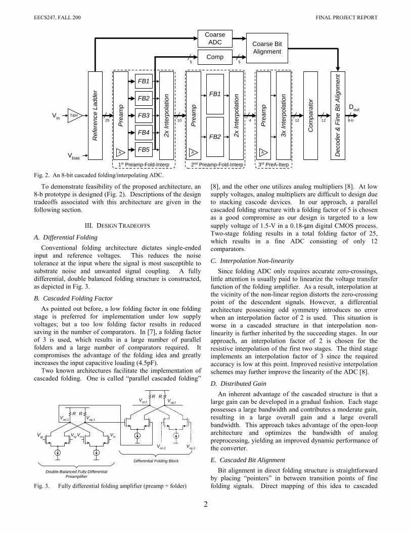
To demonstrate feasibility of the proposed architecture, an 8-b prototype is designed (Fig. 2). Descriptions of the design tradeoffs associated with this architecture are given in the following section.
III. DESIGN TRADEOFFS
A. Differential Folding Conventional folding architecture dictates single-ended
input and reference voltages. This reduces the noise tolerance at the input where the signal is most susceptible to substrate noise and unwanted signal coupling. A fully differential, double balanced folding structure is constructed, as depicted in Fig. 3.
B. Cascaded Folding Factor As pointed out before, a low folding factor in one folding
stage is preferred for implementation under low supply voltages; but a too low folding factor results in reduced saving in the number of comparators. In [7], a folding factor of 3 is used, which results in a large number of parallel folders and a large number of comparators required. It compromises the advantage of the folding idea and greatly increases the input capacitive loading (4.5pF).
Two known architectures facilitate the implementation of cascaded folding. One is called �parallel cascaded folding�
[8], and the other one utilizes analog multipliers [8]. At low supply voltages, analog multipliers are difficult to design due to stacking cascode devices. In our approach, a parallel cascaded folding structure with a folding factor of 5 is chosen as a good compromise as our design is targeted to a low supply voltage of 1.5-V in a 0.18-µm digital CMOS process. Two-stage folding results in a total folding factor of 25, which results in a fine ADC consisting of only 12 comparators.
C. Interpolation Non-linearity Since folding ADC only requires accurate zero-crossings,
little attention is usually paid to linearize the voltage transfer function of the folding amplifier. As a result, interpolation at the vicinity of the non-linear region distorts the zero-crossing point of the descendent signals. However, a differential architecture possessing odd symmetry introduces no error when an interpolation factor of 2 is used. This situation is worse in a cascaded structure in that interpolation non-linearity is further inherited by the succeeding stages. In our approach, an interpolation factor of 2 is chosen for the resistive interpolation of the first two stages. The third stage implements an interpolation factor of 3 since the required accuracy is low at this point. Improved resistive interpolation schemes may further improve the linearity of the ADC [8].
D. Distributed Gain An inherent advantage of the cascaded structure is that a
large gain can be developed in a gradual fashion. Each stage possesses a large bandwidth and contributes a moderate gain, resulting in a large overall gain and a large overall bandwidth. This approach takes advantage of the open-loop architecture and optimizes the bandwidth of analog preprocessing, yielding an improved dynamic performance of the converter.
E. Cascaded Bit Alignment Bit alignment in direct folding structure is straightforward
by placing �pointers� in between transition points of fine folding signals. Direct mapping of this idea to cascaded
FB1
FB2
FB3
FB4 2x In
terp
olat
ion
FB5
Ref
eren
ce L
adde
r
A
1st Preamp-Fold-Interp
FB1
FB2 2x In
terp
olat
ion
2nd Preamp-Fold-Interp
Prea
mp
10
A
Prea
mp
25 4
A
3x In
terp
olat
ion
3rd PreA-Iterp
Prea
mp
12
CoarseADC
T&HVin
Vbias
Comp5
Coarse BitAlignment
5
Com
para
tor
Dec
oder
& F
ine
Bit A
lignm
ent
12 8-b
Dout
Fig. 2. An 8-bit cascaded folding/interpolating ADC.
VrnVrp VinVip
R RVon,1 Vop,1
R RVon,f Vop,f
Double-Balanced Fully-DifferentialPreamplifier
Differential Folding Block
Von,2 Vop,2
Fig. 3. Fully differential folding amplifier (preamp + folder)

EECS247, FALL 200 FINAL PROJECT REPORT
3
folding case results in a brute-force implementation where a large number of coarse comparators are needed. In our 8-bit case, this number would be 5*5=25. Furthermore, these comparators cannot tolerate an offset of more than 1/25 of the full input range. Otherwise, bit alignment error will occur. This translates into a large complexity in terms of both chip area and power consumption.
A closer look at the fine folding signal reveals the possibility of a two-step offset coarse-fine bit alignment scheme. In this approach, a total of 5+5=10 coarse comparators are used, resulting in a saving of 15 comparators. Only 5 of these comparators are required to have a small offset of 6 LSBs. The other 5 can tolerate an offset as large as 1/5 of the input range.
F. Input Sample & Hold Circuit The intrinsic analog parallelism in folding/interpolating
ADC requires good matching in propagation delay between parallel signal paths and a low clock skew. This requirement can be very stringent in an 8-bit converter. A sample and hold circuit (S/H) operating at the front-end may greatly alleviate this problem. But for low supply voltages, the S/H stage may be saved at the cost of degraded performance for high-frequency input signals.
IV. RESULTS
A. 6-bit, ADC A 6-bit direct folding low complexity ADC is modeled.
Please refer to our midterm report for details.
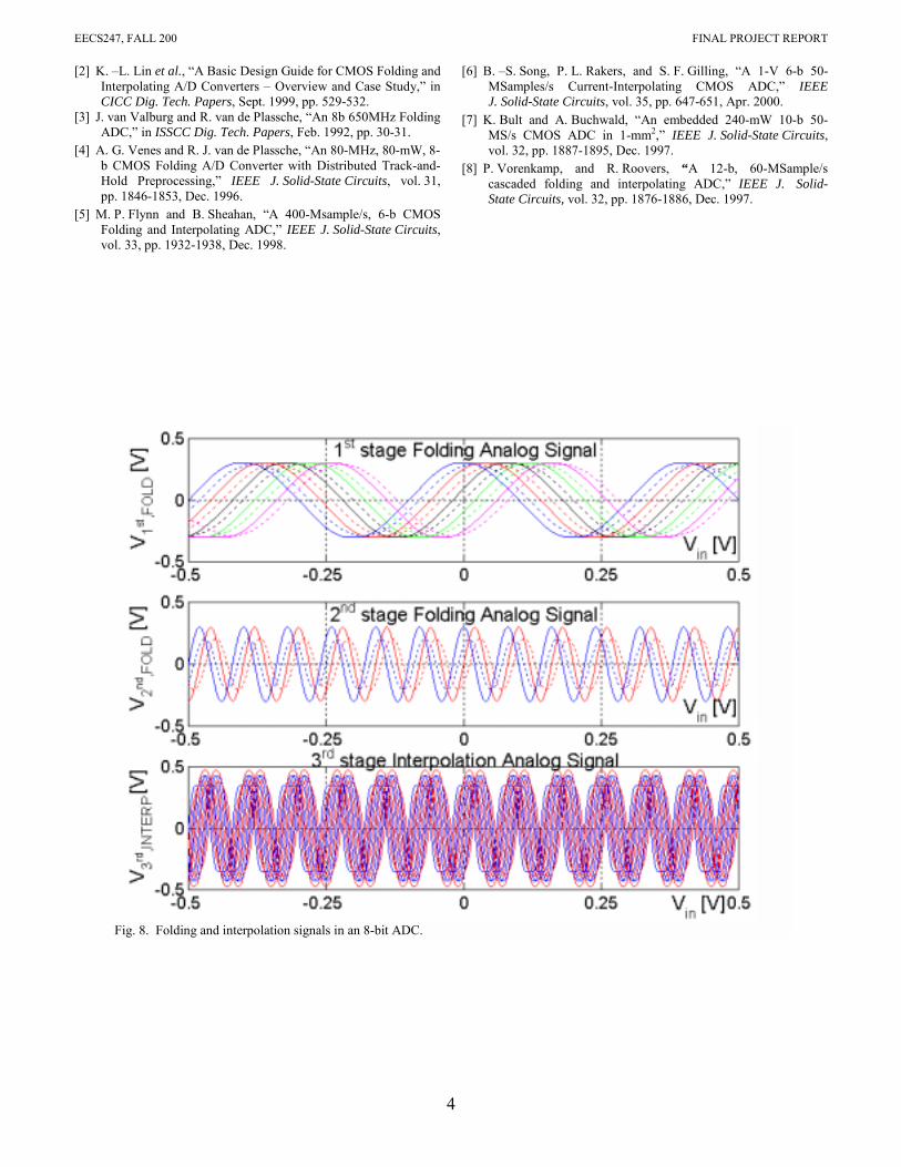
B. 8-bit ADC Cascaded folding scheme is applied to an 8-bit ADC. The
following two tables summarize the design constraints and performance of an 8-bit ADC for various circuit parameters according to SIMULINK simulation. The performance is obtained under the typical parameter values specified in Table 2. Fig. 8-12 illustrate performance of this ADC.
TABLE I: PERFORMANCE SUMMARY Resolution 8.17-bit
# of decision levels 288 Missing code No
Non-monotonic code No Full-scale input VFS 1Vpp
DNL ±0.4LSB INL ±1LSB
SFDR 58dB SNDR 47.3dB
TABLE II: SUMMARY OF DESIGN CONSTRAINTS Parameter Constraint (3σ)
Ref. ladder matching 9-bit 1st stage preamp gain matching 5-bit 2nd stage preamp gain matching 4-bit 3rd stage preamp gain matching 4-bit 1st stage folder gain matching 5-bit 2nd stage folder gain matching 4-bit 1st stage intp. R matching 4-bit 2nd stage intp. R matching 4-bit 3rd stage intp. R matching 4-bit Coarse comparator offset 100 mV Middle comparator offset 50 mV Fine comparator offset 20 mV
V. CONCLUSION
A detailed study of folding and interpolation ADC architecture is performed. A case of an 8-bit cascaded folding ADC is modeled. Various circuit and architecture parameter tradeoffs are evaluated. It is found that the dominant non-linearity error in such a converter is still the mismatch of the reference resistor ladder and the offset of the input preamps. Interpolation greatly improves DNL; however, offers little help on INL. Cascaded folding is an efficient architecture for low complexity low supply voltage implementations.
VI. REFERENCES
[1] B. Nauta and A. G. W. Venes, �A 70MSample/s 110mW 8b CMOS Folding Interpolating A/D Converter,� in ISSCC Dig. Tech. Papers, Feb. 1995, pp. 276-277.
EECS247, FALL 200 FINAL PROJECT REPORT
4
[2] K. �L. Lin et al., �A Basic Design Guide for CMOS Folding and Interpolating A/D Converters � Overview and Case Study,� in CICC Dig. Tech. Papers, Sept. 1999, pp. 529-532.
[3] J. van Valburg and R. van de Plassche, �An 8b 650MHz Folding ADC,� in ISSCC Dig. Tech. Papers, Feb. 1992, pp. 30-31.
[4] A. G. Venes and R. J. van de Plassche, �An 80-MHz, 80-mW, 8-b CMOS Folding A/D Converter with Distributed Track-and-Hold Preprocessing,� IEEE J. Solid-State Circuits, vol. 31, pp. 1846-1853, Dec. 1996.
[5] M. P. Flynn and B. Sheahan, �A 400-Msample/s, 6-b CMOS Folding and Interpolating ADC,� IEEE J. Solid-State Circuits, vol. 33, pp. 1932-1938, Dec. 1998.
[6] B. �S. Song, P. L. Rakers, and S. F. Gilling, �A 1-V 6-b 50-MSamples/s Current-Interpolating CMOS ADC,� IEEE J. Solid-State Circuits, vol. 35, pp. 647-651, Apr. 2000.
[7] K. Bult and A. Buchwald, �An embedded 240-mW 10-b 50-MS/s CMOS ADC in 1-mm2,� IEEE J. Solid-State Circuits, vol. 32, pp. 1887-1895, Dec. 1997.
[8] P. Vorenkamp, and R. Roovers, “A 12-b, 60-MSample/s cascaded folding and interpolating ADC,� IEEE J. Solid-State Circuits, vol. 32, pp. 1876-1886, Dec. 1997.
Fig. 8. Folding and interpolation signals in an 8-bit ADC.

EECS247, FALL 200 FINAL PROJECT REPORT
5
Fig. 9. 8-b ADC output due to ramp input.
Fig. 10. 8-b AND DNL and INL under ideal parameter values.

EECS247, FALL 200 FINAL PROJECT REPORT
6
Fig. 11. 8-b ADC DNL and INL plot with circuit parameters specified in Table. 1.
Fig. 12. Spectrum of the digitized sinusoidal input at 1/5 of the Nyquist frequency.

FURTHER READING
Click any one of the following links to be taken to a website which contains the following documents.
The following are some recent examples of Asynchronous ADC activity off the web.
6 bit Asynchronous December 2006Asynchronous ADC In CAD Mentor GraphicsAsynchronous Data Processing System ASYNCHRONOUS PARALLEL RESISTORLESS ADCFlash Asynchronous Analog-to-Digital ConverterNovel Asynchronous ADC ArchitectureLEVEL BASED SAMPLING FOR ENERGY CONSERVATION IN LARGE NETWORKSA Level-Crossing Flash Asynchronous Analog-to-Digital ConverterWeight functions for signal reconstruction based on level crossingsAdaptive Rate Filtering Technique Based on the Level Crossing SamplingAdaptive Level–Crossing Sampling Based DSP Systems A 0.8 V Asynchronous ADC for Energy Constrained Sensing Applications Spline-based signal reconstruction algorithm from multiple level crossing samplesA New Class of Asynchronous Analog-to-Digital ConvertersEffects of time quantization and noise in level crossing sampling stabilization
Here is some more background information on Analog to Digital converters.
A 1-GS/s 6-bit 6.7-mW ADCA Study of Folding and Interpolating ADCFolding_ADCs_Tutorialshigh speed ADC designInvestigation of a Parallel Resistorless ADC
Here are some patents on the subject.
4,291,299_Analog_to_digital_converter_using_timed4,352,999_Zero_crossing_comparators_with_threshold4,544,914_Asynchronously_controllable_successive_approximation4,558,348_Digital_video_signal_processing_system_using5,001,364_Threshold_crossing_detector5,315,284_Asynchronous_digital_threshold_detector_5,945,934_Tracking_analog_to_digital_converter6,020,840_Method_and_apparatus_for_representing_waveform6,492,929_Analogue_to_digital_converter_and_method6,501,412_Analog_to_digital_converter_including_a_quantizers6,667,707_Analog_to_digital_converter_with_asynchronous_ability6,720,901_Interpolation_circuit_having_a_conversio26,850,180_SelfTimed_ADC6,965,338_Cascade_A_D_converter7,133,791_Two_mean_level_crossing_time_interval
11.19.10_1.20PM [email protected] Sauer