A SOFTWARE-BASED FREQUENCY LOCKED LOOP … main advantage of using a software-based controller ......
12
IJRRAS 10 (1) ● January 2012 www.arpapress.com/Volumes/Vol10Issue1/IJRRAS_10_1_11.pdf 82 A SOFTWARE-BASED FREQUENCY LOCKED LOOP DC MOTOR DRIVE SYSTEM Mohammad A.K. Alia, Tariq M. Younes, Rateb H. Issa & Hussein Sarhan Mechatroncis Engineering Department, Faculty of Engineering Technology, Al-Balqa Applied University ABSTRACT The paper considers controlling DC motor speed using LabVIEW-based frequency locked loop control algorithm which consists of a set of virtual instruments. Power interface circuit is required to supply the motor. In order to realize frequency-lock; a software digital integrator is used by implementing up-down counter. Proportional control term is included in order to control the depth of integral action. The result of the experiment shows acceptable start- stop time characteristics and that motor speed is hold constant independent of motor load changes. Keywords: LabView, Phase-Lock, Digital Integration, DAC, Counter, Optical Encoder. 1. INTRODUCTION DC motors have been widely used in robotics and in industrial variable speed applications because of their desirable speed-torque characteristics and simplicity of control. Feedback motor drive is required in order to achieve high accuracy and better performance. Conventionally, this is achieved by analog servo feedback system in which any change in speed is sensed by tachometer and compared with a fixed reference voltage to generate a correction signal. However, this analog feedback system is not satisfactory where excellent speed regulation and fast dynamic response are required. These features can be achieved by using a phase-locked loop control system [1 ]. In the phase locked loop configuration, motor speed is converted to a digital pulse train, which is synchronized with a reference digital pulse train. In this way, by looking onto a reference frequency, precise control of motor speed is achieved. Reference frequency can be derived from a precision crystal controlled source or any frequency source with the required stability and accuracy. Motor speed is sensed by either a Hall Effect devices or an optical encoder. The Phase Locked Loop (PLL) may be considered as a servo system, which controls the phase of its output signal such a way that the phase error between the output phase and the reference phase reduces to a minimum [2]. Traditionally, the most basic functional block diagram of a PLL is given as in figure 1. This diagram shows the components that every PLL must have, namely: a Phase Detector (PD), a voltage controlled oscillator (VCO), a Loop Filter (LF) and a feedback interconnection. The PD is a nonlinear device whose output contains the phase difference between the two oscillating input signals. The VCO is another nonlinear device which produces an oscillation whose frequency is controlled by a lower frequency input voltage. Concerning the LF, it is a low pass filter used to suppress the noise and high frequency signal components from the PD, and provides a DC controlled signal for VCO. If the PD is linear and the PLL in lock, then the filter output is proportional to a phase error. In general this block contains the required gain and filtering to set the loop‟s overall bandwidth and meet the necessary stability criteria. 2. STRUCTURAL ANALYSIS OF MOTOR DRIVE PLL Hereinafter we shall consider three important issues, namely: the nature of VCO in motor drive loops, the extent of adequacy of existing (PDs) for motor Drives and the need of a phase-frequency or a frequency-phase detecting procedure. There are substantial differences between the PLL used for communication loops and those used for motor speed control. The VCO in conventional communication loop changes frequency very rapidly on command, while there is no real VCO in motor drive PLL. But at first glance, it seems that the motor, motor drive circuit, and the feedback speed encoder have simply replaced the VCO in the classic PLL, and they may be considered as a virtual VCO. In fact this virtual VCO is a little more complicated. The mechanical and electrical time constants of the motor more than just a voltage-in, frequency-out block. Another important issue is the nonlinear characteristics of the different types of detectors. The two most common methods of implementing PDs are (1) analog mixer and (2) digital PDs, which are implemented by sequential logic circuits. The product detectors may be considered as useless in motor drives because they produce no DC for acceleration or deceleration when out of lock, further more lockup may occur on harmonics, thereby yielding incorrect shaft speeds. Analysis of digital phase detectors shows [ ] that while the exact behavior of these digital phase detectors is necessarily nonlinear, the low frequency behavior is often linear. A good example for that is AD9901 PD. Add to that, that the characteristics of the square signal (PDs) are linear over different detection intervals. For triangle (PD) it is (-/2, +/2), for sawtooth PD it is (-, +), and for sequential phase frequency (PFD) it is (-2, +2). Thus, although there is a variety of phase detectors, no one (PD)
Transcript of A SOFTWARE-BASED FREQUENCY LOCKED LOOP … main advantage of using a software-based controller ......

IJRRAS 10 (1) ● January 2012 www.arpapress.com/Volumes/Vol10Issue1/IJRRAS_10_1_11.pdf
82
A SOFTWARE-BASED FREQUENCY LOCKED LOOP DC MOTOR
DRIVE SYSTEM
Mohammad A.K. Alia, Tariq M. Younes, Rateb H. Issa & Hussein Sarhan
Mechatroncis Engineering Department, Faculty of Engineering Technology, Al-Balqa Applied University
ABSTRACT
The paper considers controlling DC motor speed using LabVIEW-based frequency locked loop control algorithm
which consists of a set of virtual instruments. Power interface circuit is required to supply the motor. In order to
realize frequency-lock; a software digital integrator is used by implementing up-down counter. Proportional control
term is included in order to control the depth of integral action. The result of the experiment shows acceptable start-
stop time characteristics and that motor speed is hold constant independent of motor load changes.
Keywords: LabView, Phase-Lock, Digital Integration, DAC, Counter, Optical Encoder.
1. INTRODUCTION
DC motors have been widely used in robotics and in industrial variable speed applications because of their desirable
speed-torque characteristics and simplicity of control. Feedback motor drive is required in order to achieve high
accuracy and better performance. Conventionally, this is achieved by analog servo feedback system in which any
change in speed is sensed by tachometer and compared with a fixed reference voltage to generate a correction signal.
However, this analog feedback system is not satisfactory where excellent speed regulation and fast dynamic
response are required. These features can be achieved by using a phase-locked loop control system [1 ]. In the phase
locked loop configuration, motor speed is converted to a digital pulse train, which is synchronized with a reference
digital pulse train. In this way, by looking onto a reference frequency, precise control of motor speed is achieved.
Reference frequency can be derived from a precision crystal controlled source or any frequency source with the
required stability and accuracy. Motor speed is sensed by either a Hall Effect devices or an optical encoder. The
Phase Locked Loop (PLL) may be considered as a servo system, which controls the phase of its output signal such a
way that the phase error between the output phase and the reference phase reduces to a minimum [2]. Traditionally,
the most basic functional block diagram of a PLL is given as in figure 1. This diagram shows the components that
every PLL must have, namely: a Phase Detector (PD), a voltage controlled oscillator (VCO), a Loop Filter (LF) and
a feedback interconnection. The PD is a nonlinear device whose output contains the phase difference between the
two oscillating input signals. The VCO is another nonlinear device which produces an oscillation whose frequency
is controlled by a lower frequency input voltage. Concerning the LF, it is a low pass filter used to suppress the noise
and high frequency signal components from the PD, and provides a DC controlled signal for VCO. If the PD is
linear and the PLL in lock, then the filter output is proportional to a phase error. In general this block contains the
required gain and filtering to set the loop‟s overall bandwidth and meet the necessary stability criteria.
2. STRUCTURAL ANALYSIS OF MOTOR DRIVE PLL
Hereinafter we shall consider three important issues, namely: the nature of VCO in motor drive loops, the extent of
adequacy of existing (PDs) for motor Drives and the need of a phase-frequency or a frequency-phase detecting
procedure. There are substantial differences between the PLL used for communication loops and those used for
motor speed control. The VCO in conventional communication loop changes frequency very rapidly on command,
while there is no real VCO in motor drive PLL. But at first glance, it seems that the motor, motor drive circuit, and
the feedback speed encoder have simply replaced the VCO in the classic PLL, and they may be considered as a
virtual VCO. In fact this virtual VCO is a little more complicated. The mechanical and electrical time constants of
the motor more than just a voltage-in, frequency-out block. Another important issue is the nonlinear characteristics
of the different types of detectors. The two most common methods of implementing PDs are (1) analog mixer and
(2) digital PDs, which are implemented by sequential logic circuits. The product detectors may be considered as
useless in motor drives because they produce no DC for acceleration or deceleration when out of lock, further more
lockup may occur on harmonics, thereby yielding incorrect shaft speeds. Analysis of digital phase detectors shows [
] that while the exact behavior of these digital phase detectors is necessarily nonlinear, the low frequency behavior is
often linear. A good example for that is AD9901 PD. Add to that, that the characteristics of the square signal (PDs)
are linear over different detection intervals. For triangle (PD) it is (-/2, +/2), for sawtooth PD it is (-, +), and for
sequential phase frequency (PFD) it is (-2, +2). Thus, although there is a variety of phase detectors, no one (PD)

IJRRAS 10 (1) ● January 2012 Alia & al. ● Frequency Locked Loop Dc Motor Drive System
83
is optimal or even applicable in each situation. Their usefulness depends greatly on the type of PLL they will be
used in, and on the input signals that they will be encountering [3,4].
The third issue is detecting sequence. In motor drives the explicit variable is speed and not phase. PDs are used to
recover the information contained in the phase of the reference signal, where in motor drive there is no information
in the phase of the reference signal. Consequently, motor speed controls don not require phase lock, but only
integration of the frequency error ():
kdtw fr (1)
Where =2f.
Taking in consideration the above mentioned facts it is advisable to eliminate the frequency error at first, and then to
realize phase correspondence by auxiliary means as required.
3. THE BLOCK DIAGRAM OF MOTOR SPEED USING PLL
Now it is obvious that we do need a frequency motor drive loop instead of a phase motor drive loop[5]. Frequency
motor drive loop must have a pure integration in the signal path in order to reduce the error between r and f to
zero. This coincides with the fact where the traditional (PD) has a transfer function equal to K/S. Because of the
digital nature of the feedback, digital integration is recommended [5,6]. Digital integration may be realized by using
a digital up down counter, with a subsequent Digital to Analog (D/A) conversion. D/A is carried out by using
Frequency to Voltage (F/V) converter or DAC. In order to facilitate better dynamic performance to the PLL, it is
imperative to include a proportional control component in addition to the integral action. This gives the designer
possibility to soften the severity of the integral action as required. For the circuit to the work in a phase lock mode
an additional signal path is required.
Figure 1. PLL block diagram
This path starts at the LSB of the counter and includes a differential operational amplifier. The amplifier compares
the DC component of the counter LSB output to Vcc/2 [6]. Any difference in integrated and causes a change in the
speed. Only when the DC component of LSB output is exactly equal to Vcc/2 (i.e. 50% duty cycle) will integrator
amplifier output causes to change, and the phases of the speed encoder and reference frequencies are 180 apart [7].
The two signals are actually phaselocked at 180. The block diagram is shown in figure No(1),where
Km- monostable “gain”
G1- error amplifier gain (dimensionless)
M- monostable filter time constant
Ki- integration “gain” (V/count)
1, 2- op amp time constants (sec)
K- phase gain (dimensionless)
A1- transconductance (A/V)
f –carrier filter time constant (sec)
N- number of lines on the disc(dimensionless)
KT- motor torque constant (oz-in./A)
J- total inertia (oz-in.sec2)
KD- damping constant (oz-in./1000rpm)
4. PRACTICAL INVESTIGATION OF FREQUENCY LOCKED DC MOTOR DRIVE
The frequency looked motor drive controller consists of a set of virtual instruments (VIs), which are interconnected
to each other in order to realize the required control algorithm. A detailed description for the VIs is given in
appendix No(1). The required VIs are:
- Analog input acquire waveform VI
- The digital Integrator VI
- Digital to analog Converter VI
- Analog output VI

IJRRAS 10 (1) ● January 2012 Alia & al. ● Frequency Locked Loop Dc Motor Drive System
84
The main advantage of using a software-based controller [8,9] is the gained flexibility in selection of controller
parameters, tuning by that the controller in right direction. The output of the Data Acquisition (DAQ) board (PCI-
MIO-16E-1) is fed to a power interface circuit, which drive the motor. The motor is PM, Dc type with the following
parameters: supply voltage 24 V, In=0.6 mA, P=15 W, Ra=6 and the nominal speed is 1500 rpm.
The feedback incremental transmissive optical encoder was assembled at the laboratory of process control. The disk
of the encoder has 300 windows. The output of the encoder is connected to a Schmitt trigger IC (CD40105DE) in
order to square the encoder output pulses. Schmitt trigger provides standard CMOS output levels. The output of
Schmitt trigger is connected to two decade frequency dividers (CD4017B). The motor and power interface are parts
of training board type (DELLREZO-DL-2314) which exists at the laboratory of process control- Mechatronics
Engineering Department. The feedback signal is fed to a counter on the DAQ board. The frequency is measured
using software VI(period Icon VI), and the speed is measured using the formula [10]
300
60
fn (2)
The complete experimental setup is given in figure 2.
Figure 2. The experimental setup
5. EXPERIMENTAL RESULTS
Figure 3 shows no-load motor starting and stopping time characteristics.
Figure 3. No -load motor starting and stopping time characteristics

IJRRAS 10 (1) ● January 2012 Alia & al. ● Frequency Locked Loop Dc Motor Drive System
85
At the beginning the reference frequency makes the counter count to increase because it is large than the tachometric
frequency which makes the counter count to decrease. As a result of that the counter increments up rapidly trying to
reach a steady state quickly, where as each reference rising edge generates one step more and on the other side each
tachometric rising edge makes one step down. Rising time is about 0.56 s. when the tachometric frequency equals to
the reference frequency the counter count is still constant. When the motor is turned off, tachometric frequency is
higher than the reference, the counter count starts to decrease till reaching zero condition or reset state.
Figure 4 shows that the rise time is decreased when the reference frequency was increases from 41 Hz to 200 Hz.
Figure 4. Effect of frequency change on rising time
6. CONCLUSIONS
1- The feasibility of using LabVIEW –based frequency locked motor drive system is demonstrated.
Precise speed regulation, stabilization is achieved and the system has the ability to recover to the rated
speed as a result of load change.
2- The proposed system offers many advantages such as accurate speed control and digital control
possibility.
3- Realizing a software-based controller, makes it possible to tune controller parameters to match the
controlled object performance criteria, without having a rigorous identification of the controlled
process.
7. APPENDIX 1.
LabVeiw VIs used in research.
7.1 Analog input Acquire WaveForm VI
In order to control the motor speed, it is necessary to get a feedback signal which represents the instantaneous value
of the motor speed. This feedback signal shall be subtracted from a reference speed value and as a result of that
speed error will be evaluated. Feedback signal is introduced to the DAQ board using Analog input Acquire
WaveForm VI . the front panel and the block daigrm of Analog input Acquire Waveform VI are shown in figures 5
and 6.
Figure 5. Front panel of Analog Input Acquire Waveform VI

IJRRAS 10 (1) ● January 2012 Alia & al. ● Frequency Locked Loop Dc Motor Drive System
86
Figure 6. Block diagram of Analog Input Acquire Waveform VI
Function:
This VI must be supported by a data acquisition device (DAQ) board to acquire one hundred samples from the
feedback (tachometer) signal at the analog input channel with sample rate of one thousand samples /second.
Notice that the feedback input signal must range between a high limit of (+10) and a low limit of (–10) volts to be
acquiring correctly. These two limits is assembled into a cluster by Bundle VI, then we use the Build Array VI to
get an array of clusters which represent the input limits of Analog Input Acquire Waveform VI.
AI Acquire Waveform VI can configure its output to Scaled Array or Waveform data type, in our application we
select the Scaled Array option, then the array passes to Index Array VI to get the feedback signal and show it using
the feedback (tachometer) signal waveform graph.
If an error occurred, the General Error Handler VI returns a description of the error and optionally displays a
dialog box. This error is transmitted to the Unbundle Status VI to use with the stop button (when it is pressed) to
give the option of stopping the VI.
At the end of the acquiring process, the feedback (tachometer) signal passes to the following VIs.
7.2 Monostable VI
This VI generates a train of pulses as a response to an input signal. The generated pulses are with a predetermined
duration no matter what the duration of the input pulses is. Figure 7 shows the main function of the monostable VI.
Figure 7. Function of Monostable IC
It can be notified from the figure above that changing the frequency of the input signal changes the duration
(therefore the average) of the produced signal. The duration of the produced signal can be adjusted by changing the
value of the duration control in the VI.
For our application the input signal represents the feedback signal from the encoder (speed signal), while the output
train of pulses, which are produced by PC, are fed to the motor. The PC (Lab VIEW and DAQ) stands for the
monostable action
Due to the inaccurate speed-measuring device, and because of the quick variation of speed-reading, we can‟t apply
the feedback signal as the input of monostable VI. Instead of that we extract the parameters of feedback (Amplitude,
Frequency and pulse duration), after that we used them to generate a train of pulses that represent the actual
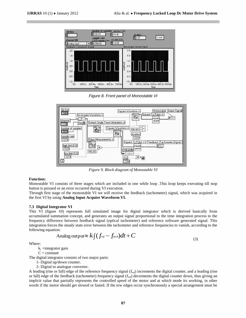
feedback signal. The Front panel and block diagram of Monostable VI are shown in figures 8 and 9.
IJRRAS 10 (1) ● January 2012 Alia & al. ● Frequency Locked Loop Dc Motor Drive System
87
Figure 8. Front panel of Monostable VI
Figure 9. Block diagram of Monostable VI
Function:
Monostable VI consists of three stages which are included in one while loop .This loop keeps executing till stop
button is pressed or an error occurred during VI execution.
Through first stage of the monostable VI we will receive the feedback (tachometer) signal, which was acquired in
the first VI by using Analog Input Acquire Waveform VI.
7.3 Digital Integrator VI
This VI (figure 10) represents full simulated image for digital integrator which is derived basically from
accumulated summation concept, and generates an output signal proportional to the time integration process to the
frequency difference between feedback signal (optical tachometer) and reference software generated signal. This
integration forces the steady state error between the tachometer and reference frequencies to vanish, according to the
following equation:
Cdtffk tachrefi )( output Analog (3)
Where:
ki =integrator gain
C = constant
The digital integrator consists of two major parts:
1- Digital up/down counter.
2- Digital to analogue converter.
A leading (rise or fall) edge of the reference frequency signal (fref) increments the digital counter, and a leading (rise
or fall) edge of the feedback (tachometer) frequency signal (fref) decrements the digital counter down, thus giving an
implicit value that partially represents the controlled speed of the motor and at which mode its working, in other
words if the motor should get slowed or fasted. If the tow edges occur synchronously a special arrangement must be

IJRRAS 10 (1) ● January 2012 Alia & al. ● Frequency Locked Loop Dc Motor Drive System
88
applied to avoid count ambiguities, the up/down counting output connected to software DAC for both positive and
negative values that produces an analogue output directly proportional to the stored binary number.
Assuming that the motor starts from rest, at the beginning the reference frequency drives the counter contents up
very rapidly, because very few count down edges are produced by the slowly rotating motor. As the counter contents
increase, an increasing error voltage is developed at the output of the D/A converter. This error voltage is fed to the
motor, which speeds up, thereby causing more count down edges. As ftach approaches fref, the counter contents in-
creases slowly. At the instant, when ftach = fref the counter contents remains stationary. The stored count develops
just enough output to drive the motor towards equilibrium by keeping fref = ftach, thereby producing a “frequency
locked” condition. Note that this is not true phase lock, because the phases are not detected yet.
Figure 10. Front panel of Digital Integrator VI
Function
Digital Integrator VI consists of four stages, as in the monostable vi these stages are included in a while loop with
stop button connected to it‟s conditional terminal, therefore, the VI keeps executing until the stop button is pressed
or an error occurred during the vi execution.It is possible to control the delay time (in milliseconds) between the
loop iterations by manipulating the value Millisecond Multiple.
The block diagram of the first stage digital integrator is shown in figure 11. In the first stage we generate the
reference signal inside a continuous while loop. Using a Square waveform VI, that generates a square waveform
with adjustable Frequency, Amplitude, and Phase parameters, then we get the reference signal by converting this
square waveform to a pulse (1 and 0 amplitude) by using Square To Pulse VI, after that this reference signal is fed
to the third stage immediately.
Figure 11. The block diagram of first stage digital integrator VI
In digital integrator VI second stage(figure 12) we will receive the feedback (tachometer) signal, which was
acquired in the analog input Acquire Waveform VI, with the help of data acquisition device (DAQ).
Due to the inaccurate speed-measuring device, we can‟t apply the feedback signal as the input of digital integrator
VI. Instead of that we extract the feedback signal parameters (Amplitude, Phase, and frequency) by using the
Extract Single Tone Information VI, and Pulse Measurements VI, that described in details in the previous VI.

IJRRAS 10 (1) ● January 2012 Alia & al. ● Frequency Locked Loop Dc Motor Drive System
89
After that we use the extracted parameters to generate a train of pulses that represent the real feedback signal using a
Square waveform VI, that generates a square waveform with adjustable Frequency, Amplitude, and Phase
parameters, then we get the Feedback (Tachometer) Signal by converting this square waveform to a pulse (1 and 0
amplitude) by using Square To Pulse VI.
After monitoring this Signal by using Feedback (Tachometer) Signal waveform graph, it is fed to the third stage
immediately.
Figure 12. The second stage of block diagram of digital integrator VI
The most important stage in the digital integrator VI is the third one which is shown in figure 13. In this stage we
detect the leading (rising) edges of both the Reference and the Feedback Signals by the assistance of two while
loop‟s shift registers:
Reference shift register for reference signal and Feedback shift register for feedback signal, then we use the Get
Y Value vi, that returns the amplitude value from the input signal specified in index which we connect to an 1024
times counter by Index shift register, the 1024 count is due to software and hardware capabilities.
In our case we need two shift register elements to remember the last two iteration values (the latest value at the
top element), so the process of detecting the rising edge is done while the two-shift register elements transfer the
signals amplitude values from one loop iteration to the next one, so we can compare these amplitudes by the use of
Greater? VI that returns a Boolean indication when a rising edge has just occurred .In other words when the latest
(top) amplitude value is greater than the previous one (below).
Figure 13. The third stage of block diagram of digital integrator VI
In the fourth stage (figure 14) we use Up\Down Count shift register (to round the Up\Down Count value between
the while loop iterations) and three nested case structures (shown in figure 15) (controlled by the Boolean
indication) to enable the reference signal's rising edges to increment the up\down count (this appears in the second
true case), and to enable the feedback signal „s rising edges to decrement it (this appears in the third true case). In

IJRRAS 10 (1) ● January 2012 Alia & al. ● Frequency Locked Loop Dc Motor Drive System
90
order to avoid count ambiguities If the two rising edges occurred synchronously a special case is added to ignore the
two edges (this appears in the first true case, and the third false case).
Note: The shift register must be initialized by the zero initial value to reset the shift register for every execution for
the while loop.
Due to the sign of the count‟s (positive or negative), the count value is fed to the positive or to the negative 16-bit
Digital To Analog Converter (DAC) VI (which will be described later) to produce an analogue output directly
proportional to the stored binary number. This analog output is shown by using u\d count waveform graph, which is
included in one time running For Loop, and the Positive and Negative least significant bits is monitored by using
two Boolean indicators.
Figure 14. The fourth stage of the block diagram of digital integrator VI
Figure 15. The three cases of the block diagram of digital integrator VI
7.4 Digital To Analog Converter (DAC) VI
The digital to analog converter, better known as the DAC, is a major interface circuit that forms the bridge between
the analog and digital worlds. DACs are the core of many circuits and in displays, and many computers – controlled
devices.
A DAC is an electronic component that converts digital logic levels (bits) into an analog voltage. The output of a
DAC is the arithmetic sum of all the input bits weighted in a particular manner:

IJRRAS 10 (1) ● January 2012 Alia & al. ● Frequency Locked Loop Dc Motor Drive System
91
15
0
i
i
WiBiDAC (4)
Where:
Wi : The weighting factor
Bi : The bit value (1 or 0)
i : The index of the bit number, In the case of a binary weighting Wi = 2i
The front panel of 16-bit DAC VI is shown in figure 16.
Figure 16. The front panel 16 –bit DAC VI
Figures 17 and 18 show the block diagram for positive and negative 16 –bit DAC.
Figure 17. The block diagram for positive 16 –bit DAC
IJRRAS 10 (1) ● January 2012 Alia & al. ● Frequency Locked Loop Dc Motor Drive System
92
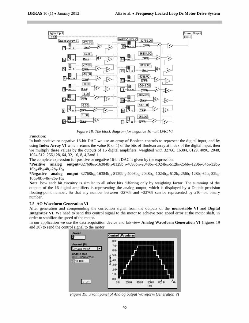
Figure 18. The block diagram for negative 16 –bit DAC VI
Function:
In both positive or negative 16-bit DAC we use an array of Boolean controls to represent the digital input, and by
using Index Array VI which returns the value (0 or 1) of the bits of Boolean array at index of the digital input, then
we multiply these values by the outputs of 16 digital amplifiers, weighted with 32768, 16384, 8129, 4096, 2048,
1024,512, 256,128, 64, 32, 16, 8, 4,2and 1.
The complete expression for positive or negative 16-bit DAC is given by the expression:
*Positive analog output=32768b15-16384b14-8129b13-4096b12-2048b11-1024b10-512b9-256b8-128b7-64b6-32b5-
16b4-8b3-4b2-2b1-1b0
*Negative analog output=32768b15-16384b14-8129b13-4096b12-2048b11-1024b10-512b9-256b8-128b7-64b6-32b5-
16b4-8b3-4b2-2b1-1b0
Note: how each bit circuitry is similar to all other bits differing only by weighting factor. The summing of the
outputs of the 16 digital amplifiers is representing the analog output, which is displayed by a Double-precision
floating-point number. So that any number between -32768 and +32768 can be represented by a16- bit binary
number.
7.5 AO Waveform Generation VI
After generation and compounding the correction signal from the outputs of the monostable VI and Digital
Integrator VI, We need to send this control signal to the motor to achieve zero speed error at the motor shaft, in
order to stabilize the speed of the motor.
In our application we use the data acquisition device and lab view Analog Waveform Generation VI (figures 19
and 20) to send the control signal to the motor.
Figure 19. Front panel of Analog output Waveform Generation VI

IJRRAS 10 (1) ● January 2012 Alia & al. ● Frequency Locked Loop Dc Motor Drive System
93
Figure 20. Block diagram of Analog output Waveform Generation VI
Function
This VI must be supported by a data acquisition device (DAQ) board to generate one thousand update /second from
the control signal at the analog output channel.
Notice that the feedback input signal must range between a high limit of (+10) and a low limit of (–10) volts to be
generated correctly. These two limits is assembled into a cluster by Bundle VI, then we use the Build Array VI to
get an array of clusters which represent the input limits of Analog Output Waveform Generation VI.
Analog output Waveform Generation VI can configure its input to Scaled Array or Waveform data type, in our
application we select the Scaled Array option, so we use the build Array VI to get the control Waveform ,and show
it using the control signal waveform graph.
If an error occurred, the General Error Handler VI returns a description of the error and optionally displays a
dialog box. This error is transmitted to the Unbundle Status VI to use with the stop button (when it is pressed) to
give the option of stopping the VI.
At the end of the generation process, the control waveform signal passes to the motor.
8. REFERENCES
[1] Phase lock loops and frequency synthesis , Venceslav F. Kroupa, John Wiley and Sons LTD, 2003. Chichester
UK. ISBN 0-470-84866-9.
[2] Ultrahigh speed phase/frequency discriminator . Analog devices, Inc,1999, AD9901, Noorwood, Ma02062-
9106, USA.
[3] Phase Locked Loop techniques – A survey Guan-Chyun, James C. Hung, IEEE transaction on Industrial
Electronics Vol 43, N 6, December 1996.
[4] Design Notes on precision phase locked speed control for DC motors, Unitrode Corporation- 1999, 7
continental BLVD, Merrimack, NH 030 USA.
[5] Phase locked loops: A control Centric Tutorial. Daniel Abramovitch, Agilent Albratories, communication and
optics research Lab, 3500 DeeCreek Road, M/S:250-9 Palo Alto, CA 94304, USA.
[6] Speed Control DC Motor under varying load using phase-locked loop systems, Wisnu Djatmiko, Bamang
Sutopo, Proceeding of international conference on electrical, electronics, communication and information.
CECI.2001, March 7-8, Jakarta.
[7] Phase lock Loops for DC Motor speed control , Dana F. Geiger, Johan Wiley and Sons, 1981, New York,
USA.
[8] Phase-Locked Loops, Design, Simulation and applications, Rolan E. Best, sixth edition, Mc Graw Hill, 2007 ,
New York, USA.
[9] Phase Locked Loop Circuit Design, Worceste Polytechnic Institute, Prentice Hall, 1991, New Jersey, USA,
ISBN 0-13-662743-9.
[10] Phase Lock Basic, William F. Egan, PhD Conta Clara University John Wiley and Soms, INC. Publication, 2n
edition,2007, USA.