A SIMPLE 1-BYTE 1-CLOCK RC4 HARDWARE …A SIMPLE 1-BYTE 1-CLOCK RC4 HARDWARE DESIGN AND ITS...
10
A SIMPLE 1-BYTE 1-CLOCK RC4 HARDWARE DESIGN AND ITS IMPLEMENTATION IN FPGA COPROCESSOR FOR SECURED ETHERNET COMMUNICATION Rourab Paul 1 , Sangeet Saha 2 , J K M Sadique Uz Zaman 3 , Suman Das 4 , Amlan Chakrabarti 5 and Ranjan Ghosh 6 Email :{rourabpaul 1 , sangeet.saha87 2 , jkmsadique 3 , aami.suman 4 }@gmail.com, [email protected] 5 , [email protected] 6 A.K.Choudhury School of Information Technology 1,5 , Dept. of Computer Science and Engineering 2 and Institute of Radio Physics and Electronics 3,4,6 , University of Calcutta, 92 A. P. C. Road, Kolkata – 700 009, India Abstract In the field of cryptography till date the 1-byte in 1-clock is the best known RC4 hardware design [1], while the 1-byte in 3clocks is the best known implementation [2,3]. The design algorithm in [1] considers two consecutive bytes together and processes them in 2 clocks. The design of 1-byte in 3-clocks is too much modular and clock hungry. In this paper considering the RC4 algorithm, as it is, a simpler RC4 hardware design providing higher throughput is proposed in which 1-byte is processed in 1-clock. In the design two sequential tasks are executed as two independent events during rising and falling edges of the same clock and the swapping is directly executed using a MUX-DEMUX combination. The power consumed in behavioral and structural designs of RC4 are estimated and a power optimization technique is proposed. The NIST statistical test suite is run on RC4 key streams in order to know its randomness property. The encryption and decryption designs are respectively embedded on two FPGA boards with RC4 in a custom coprocessor followed by Ethernet communication. Keywords: Cryptography, RC4, Stream Cipher, Hardware Design, FPGA, Coprocessor, X-power. 1. Introduction RC4 is a widely used stream cipher whose algorithm is very simple. It has withstood the test of time in spite of its simplicity. The RC4 was proposed by Ron Rivest in 1987 for RSA Data Security and was kept as trade secret till 1994 when it was leaked out [4]. Today RC4 is a part of many network protocols, e.g. SSL, TLS, WEP, WPA and many others. There were many cryptanalysis to look into its key weaknesses [4, 5] followed by many new stream ciphers [6, 7]. RC4 is still the popular stream cipher since it is executed fast and provides high security. There exist hardware implementations of some of the stream ciphers in the literature [8-11]. Since about 2003 when FPGA technology has been matured to provide cost effective solutions, many researchers started hardware implementation of RC4 as a natural fall out [2,3]. The FPGA technology turns out to be attractive since it provides soft core processor having design specific functional capability of a main processor (MicroBlaze [12]) along with reconfigurable logic blocks that can be synthesized to a desired custom coprocessor, embedded memories and IP cores. One can design RC4 algorithm totally as an executable code for the soft core processor (main processor) only or in custom coprocessor hardware operated by the main processor. Because of the system overhead, any single instruction if executed in the main processor takes at least 3 clocks, while the identical one when executed in a coprocessor takes 1-clock as the latter is customized
Transcript of A SIMPLE 1-BYTE 1-CLOCK RC4 HARDWARE …A SIMPLE 1-BYTE 1-CLOCK RC4 HARDWARE DESIGN AND ITS...
A SIMPLE 1-BYTE 1-CLOCK RC4 HARDWARE DESIGN AND ITS IMPLEMENTATION IN FPGA COPROCESSOR
FOR SECURED ETHERNET COMMUNICATION Rourab Paul1, Sangeet Saha2, J K M Sadique Uz Zaman3, Suman Das4,
Amlan Chakrabarti5 and Ranjan Ghosh6
Email :{rourabpaul1, sangeet.saha872, jkmsadique3, aami.suman4}@gmail.com, [email protected], [email protected]
A.K.Choudhury School of Information Technology1,5 , Dept. of Computer Science and Engineering2 and Institute of Radio Physics and Electronics3,4,6,
University of Calcutta, 92 A. P. C. Road, Kolkata – 700 009, India
Abstract In the field of cryptography till date the 1-byte in 1-clock is the best known RC4 hardware design [1], while the
1-byte in 3clocks is the best known implementation [2,3]. The design algorithm in [1] considers two
consecutive bytes together and processes them in 2 clocks. The design of 1-byte in 3-clocks is too much
modular and clock hungry. In this paper considering the RC4 algorithm, as it is, a simpler RC4 hardware design
providing higher throughput is proposed in which 1-byte is processed in 1-clock. In the design two sequential
tasks are executed as two independent events during rising and falling edges of the same clock and the
swapping is directly executed using a MUX-DEMUX combination. The power consumed in behavioral and
structural designs of RC4 are estimated and a power optimization technique is proposed. The NIST statistical
test suite is run on RC4 key streams in order to know its randomness property. The encryption and decryption
designs are respectively embedded on two FPGA boards with RC4 in a custom coprocessor followed by
Ethernet communication.
Keywords: Cryptography, RC4, Stream Cipher, Hardware Design, FPGA, Coprocessor, X-power.
1. Introduction RC4 is a widely used stream cipher whose algorithm is very simple. It has withstood the test of time in
spite of its simplicity. The RC4 was proposed by Ron Rivest in 1987 for RSA Data Security and was kept as
trade secret till 1994 when it was leaked out [4]. Today RC4 is a part of many network protocols, e.g. SSL,
TLS, WEP, WPA and many others. There were many cryptanalysis to look into its key weaknesses [4, 5]
followed by many new stream ciphers [6, 7]. RC4 is still the popular stream cipher since it is executed fast and
provides high security.
There exist hardware implementations of some of the stream ciphers in the literature [8-11]. Since
about 2003 when FPGA technology has been matured to provide cost effective solutions, many researchers
started hardware implementation of RC4 as a natural fall out [2,3]. The FPGA technology turns out to be
attractive since it provides soft core processor having design specific functional capability of a main processor
(MicroBlaze [12]) along with reconfigurable logic blocks that can be synthesized to a desired custom
coprocessor, embedded memories and IP cores. One can design RC4 algorithm totally as an executable code for
the soft core processor (main processor) only or in custom coprocessor hardware operated by the main
processor. Because of the system overhead, any single instruction if executed in the main processor takes at
least 3 clocks, while the identical one when executed in a coprocessor takes 1-clock as the latter is customized
to handle the specific task. Besides the clock advantage, the coprocessor based design makes the system
throughput faster by another fold since it is executed in parallel with the main processor.
In this paper, RC4 algorithm is considered as it is and exploiting conventional VHDL features a design
methodology is proposed processing of 1-byte in 1-clock. The said design is implemented in a custom
coprocessor functioning in parallel with a main processor (Xilinx Spartan3E XC3S500e-FG320 FPGA
architecture) followed by secured data communication between two FPGA boards through their respective
Ethernet ports – each of the two boards performs RC4 encryption and decryption engines separately. The
performance of our design in terms of number of clocks proved to be better than the previous works [1 – 3]. The
clock gating technology is introduced to save dynamic power. In order to see the resilience of RC4, a battery of
statistical tests as mentioned in the NIST document [14] is undertaken and it is found that the randomness
property of its key streams is reasonably good.
The paper is organized as follows. The RC4 algorithm is briefly described in Sec. 2. In Sec. 3 the
1-byte-1-clock design and its hardware implementations are described. The communication experiment set up
along with the results of relative comparisons is narrated in Sec. 4. The power optimization using clock gating
technology is discussed in Sec.5. The randomness test of RC4 algorithm undertaken following the NIST
statistical tests suite is discussed in Sec. 6 along with its results. The conclusion is discussed in Sec. 7.
2. RC4 Algorithm RC4 has a S-Box S[N], N = 0 to 255 and a secret key, key[l] where l is typically between 5 and 16,
used to scramble the S-Box [N]. It has two sequential processes, namely KSA (Key Scheduling Algorithm) and
PRGA (Pseudo Random Generation Algorithm) which are stated below in Algorithms 1 and 2 respectively. Algorithm 1: KSA Algorithm 2: PRGA
3. Hardware Implementation of 1-byte 1-clock design
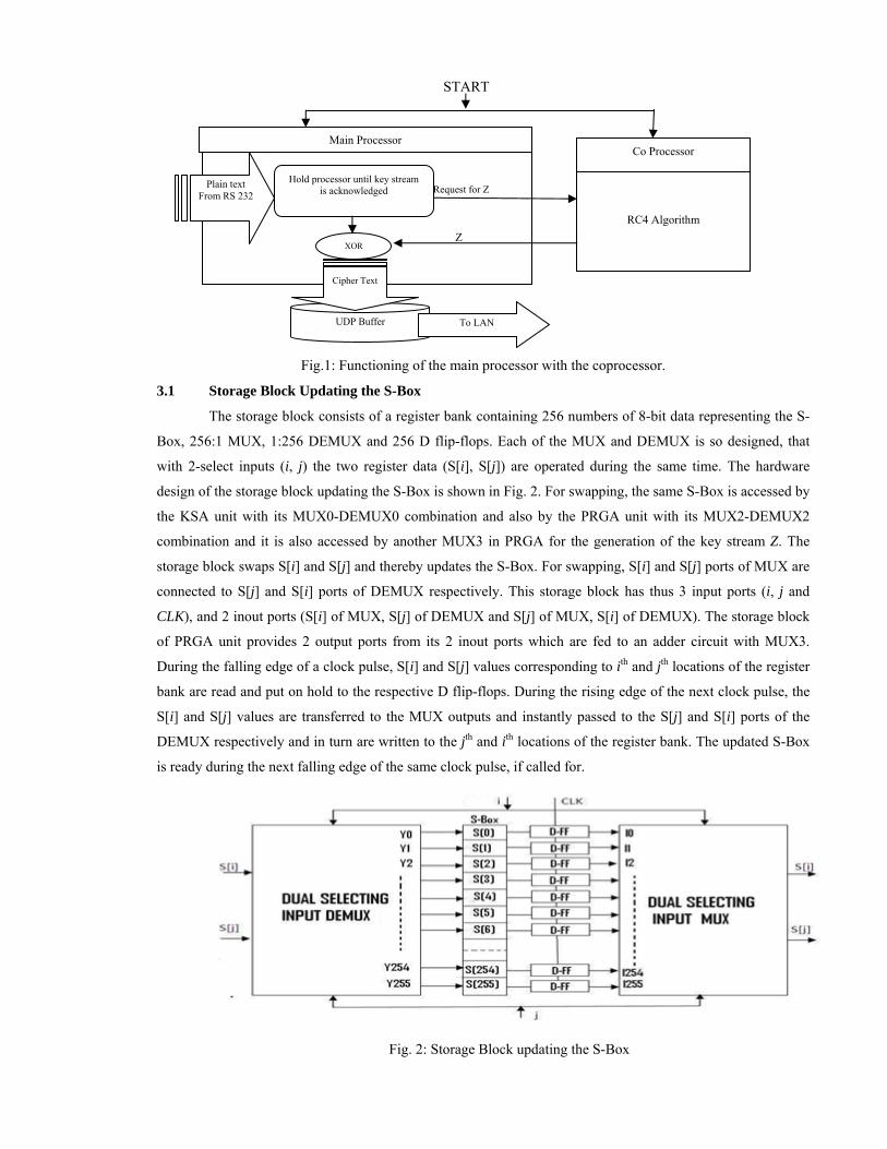
Fig. 1 shows key operations performed by the main processor in conjunction with a coprocessor till the
ciphering of the last text character. The hardware for realizing RC4 algorithm comprises of KSA and PRGA
units, which are designed in the coprocessor as two independent units, and the XOR operation is designed to be
done in the main processor. The central idea of the present embedded system implementation of one RC4 byte
in 1-clock is the hardware design of a storage block shown in Fig. 2, which is used in the KSA as well as in the
PRGA units. The storage block contains a common S-Box connected to dual select MUX-DEMUX
combination and executes the swap operation following line 9 of Algorithm 1 and line 6 of Algorithm 2, in
order to update the S-Box. The swap operation in hardware is explained in the following sub-section.
1. N = 256; 2. for i = 0 to (N-1) //Initialization module 3. S[i] = i; // Identity permutation 4. K[i] = key[i % l]; 5. end for; 6. j = 0; //Storage module 7. for i = 0 to (N-1) 8. j = (j + S[i] + K[i]) % N; 9. swap (S[i], S[j]); 10. end for;
1. N = 256; 2. i = j = 0; 3. while (TRUE)//Generating Key stream Z 4. i = (i + 1) % N; 5. j = (j + S[i]) % N; 6. swap (S[i] , S[j]); 7. t = (S[i] + S[j]) % N 8. output Z = S[t]; 9. end while;
START
Fig.1: Functioning of the main processor with the coprocessor.
3.1 Storage Block Updating the S-Box
The storage block consists of a register bank containing 256 numbers of 8-bit data representing the S-
Box, 256:1 MUX, 1:256 DEMUX and 256 D flip-flops. Each of the MUX and DEMUX is so designed, that
with 2-select inputs (i, j) the two register data (S[i], S[j]) are operated during the same time. The hardware
design of the storage block updating the S-Box is shown in Fig. 2. For swapping, the same S-Box is accessed by
the KSA unit with its MUX0-DEMUX0 combination and also by the PRGA unit with its MUX2-DEMUX2
combination and it is also accessed by another MUX3 in PRGA for the generation of the key stream Z. The
storage block swaps S[i] and S[j] and thereby updates the S-Box. For swapping, S[i] and S[j] ports of MUX are
connected to S[j] and S[i] ports of DEMUX respectively. This storage block has thus 3 input ports (i, j and
CLK), and 2 inout ports (S[i] of MUX, S[j] of DEMUX and S[j] of MUX, S[i] of DEMUX). The storage block
of PRGA unit provides 2 output ports from its 2 inout ports which are fed to an adder circuit with MUX3.
During the falling edge of a clock pulse, S[i] and S[j] values corresponding to ith and jth locations of the register
bank are read and put on hold to the respective D flip-flops. During the rising edge of the next clock pulse, the
S[i] and S[j] values are transferred to the MUX outputs and instantly passed to the S[j] and S[i] ports of the
DEMUX respectively and in turn are written to the jth and ith locations of the register bank. The updated S-Box
is ready during the next falling edge of the same clock pulse, if called for.
Fig. 2: Storage Block updating the S-Box
RC4 Algorithm
Co Processor
UDP Buffer
Request for Z
Z
Main Processor
Hold processor until key stream is acknowledged
Plain text From RS 232
XOR
Cipher Text
To LAN
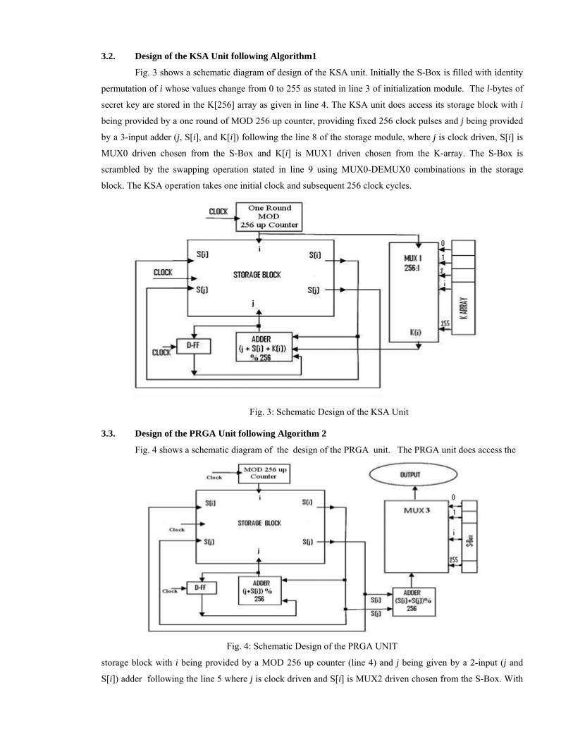
3.2. Design of the KSA Unit following Algorithm1
Fig. 3 shows a schematic diagram of design of the KSA unit. Initially the S-Box is filled with identity
permutation of i whose values change from 0 to 255 as stated in line 3 of initialization module. The l-bytes of
secret key are stored in the K[256] array as given in line 4. The KSA unit does access its storage block with i
being provided by a one round of MOD 256 up counter, providing fixed 256 clock pulses and j being provided
by a 3-input adder (j, S[i], and K[i]) following the line 8 of the storage module, where j is clock driven, S[i] is
MUX0 driven chosen from the S-Box and K[i] is MUX1 driven chosen from the K-array. The S-Box is
scrambled by the swapping operation stated in line 9 using MUX0-DEMUX0 combinations in the storage
block. The KSA operation takes one initial clock and subsequent 256 clock cycles.
Fig. 3: Schematic Design of the KSA Unit
3.3. Design of the PRGA Unit following Algorithm 2
Fig. 4 shows a schematic diagram of the design of the PRGA unit. The PRGA unit does access the
Fig. 4: Schematic Design of the PRGA UNIT
storage block with i being provided by a MOD 256 up counter (line 4) and j being given by a 2-input (j and
S[i]) adder following the line 5 where j is clock driven and S[i] is MUX2 driven chosen from the S-Box. With
up
co
st
3.
φ0
th
op
T
Th
fr
R
F
R
F
R
F
Th
fir
ge
4.
en
(D
in
al
is
na
pdated j and c
ombination of
tream Z is selec
.4 Timing
Let φi d
0. It is observe
he rising edge
perations are sh
Timing Analysi
he MOD 256 u
rom 0 to 255 fo
Rising edge of
alling edge of
Rising edge of
alling edge of
Rising edge of
alling edge of
he series conti
rst round and t
enerating Zn, th
. ExperTwo X
ngines separate
DTE) through R
n the Microbla
lgorithm comp
s implemented
arrated in Tabl
current i, the s
the storage blo
cted from the S
g analysis of th
denotes the ith
ed that a signal
of the previou
hown in Fig. 5
is of PRGA
up counter sho
or each 256 sub
φ0: Initialize j0
φ0: Start count
φ1: S[i1]↔S[j1
φ1: i2→2; j2=(j
φ2: S[i2]↔S[j2
φ2: i3→3; j3=(j
inues generatin
the clock repea
he PRGA requ
rimental SeXilinx FPGA S
ely and shown
RS 232 ports.
aze softcore p
prising KSA an
in the main pro
le 1.
swapping of S
ock. Following
S-Box using M
he PRGA Ope
clock cycle fo
l value gets up
us clock cycle
.
Fig. 5. Clock-
own in Fig. 4 is
bsequent clock
0 = 0.
ter i1 =1; j1=(j0
1]; Z1=(S[i1]+S
j1+S[i2])%256;
2]; Z2=(S[i2]+S
j2+S[i3])%256;
ng successive
ats (n+1) times
ires (n+1) cloc
tup and ReSpartan3E (XC
n in Fig 6, are c
Two experime
processor [12]
nd PRGA units
ocessor using S
S[i] and S[j] is
g the line 7, S
MUX 3 (line 8).
eration
r i ≥ 0. It is as
pdated during a
. The symbol
-wise descripti
s so designed t
k cycles.
0 + S[i1])%256;
S[j1])%256 = 1s
; Read S[i2], S[
S[j2])%256 = 2n
; Read S[i3], S[
keys (Z’s). If
s. After genera
cks and its thro
sults 3S500e-FG320
connected thro
ents are undert
] and its code
s is designed in
System C. The
s executed foll
[i] and S[j] giv
ssumed that the
a falling edge
↔ indicates s
on of PRGA o
that i starts fro
; Read S[i1],S[jst Key stream.
[j2]. nd Key stream.
[j3].
the text charac
ting Zn during
oughput per byt
0) boards, each
ough Ethernet p
taken. In expt
e was written
n a coprocesso
e hardware reso
lowing line 6
ve a value of t
e PRGA unit s
of a clock cyc
swap operation
operation
om 1, goes up t
j1].
cters are n and
the rising edg
te is (1+1/n).
h with RC4 en
ports and to re
. 1, the whole
using system
or using VHDL
ource usage for
using MUX2-
t based on whi
starts when clo
le if it is chan
n. The clock-w
to 255 and then
d n > 254, i =
e of φn, PGRA
ncryption and
espective hyper
design was im
C. In expt. 2
L and the XOR
r experiments
-DEMUX2
ich the key
ck cycle is
ged during
wise PRGA
n it repeats
0 after the
A stops. For
decryption
r terminals
mplemented
2, the RC4
R operation
1 and 2 are
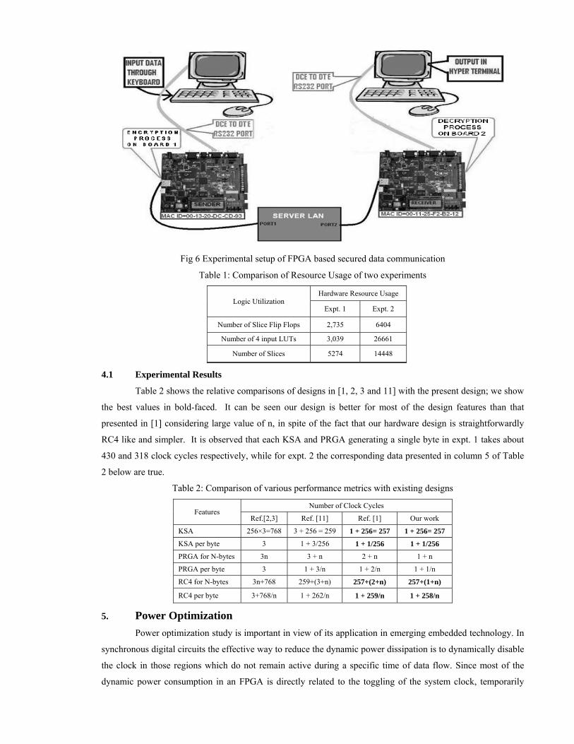
Fig 6 Experimental setup of FPGA based secured data communication
Table 1: Comparison of Resource Usage of two experiments
Logic Utilization Hardware Resource Usage
Expt. 1 Expt. 2
Number of Slice Flip Flops 2,735 6404
Number of 4 input LUTs 3,039 26661
Number of Slices 5274 14448
4.1 Experimental Results
Table 2 shows the relative comparisons of designs in [1, 2, 3 and 11] with the present design; we show
the best values in bold-faced. It can be seen our design is better for most of the design features than that
presented in [1] considering large value of n, in spite of the fact that our hardware design is straightforwardly
RC4 like and simpler. It is observed that each KSA and PRGA generating a single byte in expt. 1 takes about
430 and 318 clock cycles respectively, while for expt. 2 the corresponding data presented in column 5 of Table
2 below are true.
Table 2: Comparison of various performance metrics with existing designs
Features Number of Clock Cycles
Ref.[2,3] Ref. [11] Ref. [1] Our work
KSA 256×3=768 3 + 256 = 259 1 + 256= 257 1 + 256= 257
KSA per byte 3 1 + 3/256 1 + 1/256 1 + 1/256
PRGA for N-bytes 3n 3 + n 2 + n 1 + n
PRGA per byte 3 1 + 3/n 1 + 2/n 1 + 1/n
RC4 for N-bytes 3n+768 259+(3+n) 257+(2+n) 257+(1+n)
RC4 per byte 3+768/n 1 + 262/n 1 + 259/n 1 + 258/n
5. Power Optimization
Power optimization study is important in view of its application in emerging embedded technology. In
synchronous digital circuits the effective way to reduce the dynamic power dissipation is to dynamically disable
the clock in those regions which do not remain active during a specific time of data flow. Since most of the
dynamic power consumption in an FPGA is directly related to the toggling of the system clock, temporarily
disabling the clock in inactive regions is the most straightforward method of minimizing power consumption.
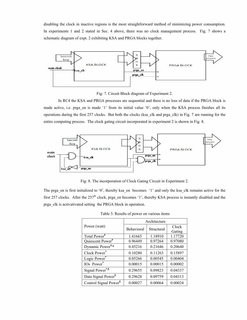
In experiments 1 and 2 stated in Sec. 4 above, there was no clock management process. Fig. 7 shows a
schematic diagram of expt. 2 exhibiting KSA and PRGA blocks together.
Fig: 7. Circuit Block diagram of Experiment 2.
In RC4 the KSA and PRGA processes are sequential and there is no loss of data if the PRGA block is
made active, i.e. prga_en is made ‘1’ from its initial value ‘0’, only when the KSA process finishes all its
operations during the first 257 clocks. But both the clocks (ksa_clk and prga_clk) in Fig. 7 are running for the
entire computing process. The clock gating circuit incorporated in experiment 2 is shown in Fig. 8.
Fig: 8. The incorporation of Clock Gating Circuit in Experiment 2. The prga_en is first initialized to ‘0’, thereby ksa_en becomes ‘1’ and only the ksa_clk remains active for the
first 257 clocks. After the 257th clock, prga_en becomes ‘1’, thereby KSA process is instantly disabled and the
prga_clk is activativated setting the PRGA block in operation.
Table 3. Results of power on various items
Power (watt) Architecture
Behavioral Structural Clock Gating
Total Power# 1.41665 1.18910 1.17720 Quiescent Power# 0.96449 0.97264 0.97080 Dynamic Power#,* 0.45216 0.21646 0.20640 Clock Power* 0.10280 0.11263 0.15897 Logic Power* 0.05266 0.00545 0.00404 IOs Power* 0.00015 0.00015 0.00002 Signal Power*,$ 0.29655 0.09823 0.04337 Data Signal Power$ 0.29628 0.09759 0.04313 Control Signal Power$ 0.00027 0.00064 0.00024
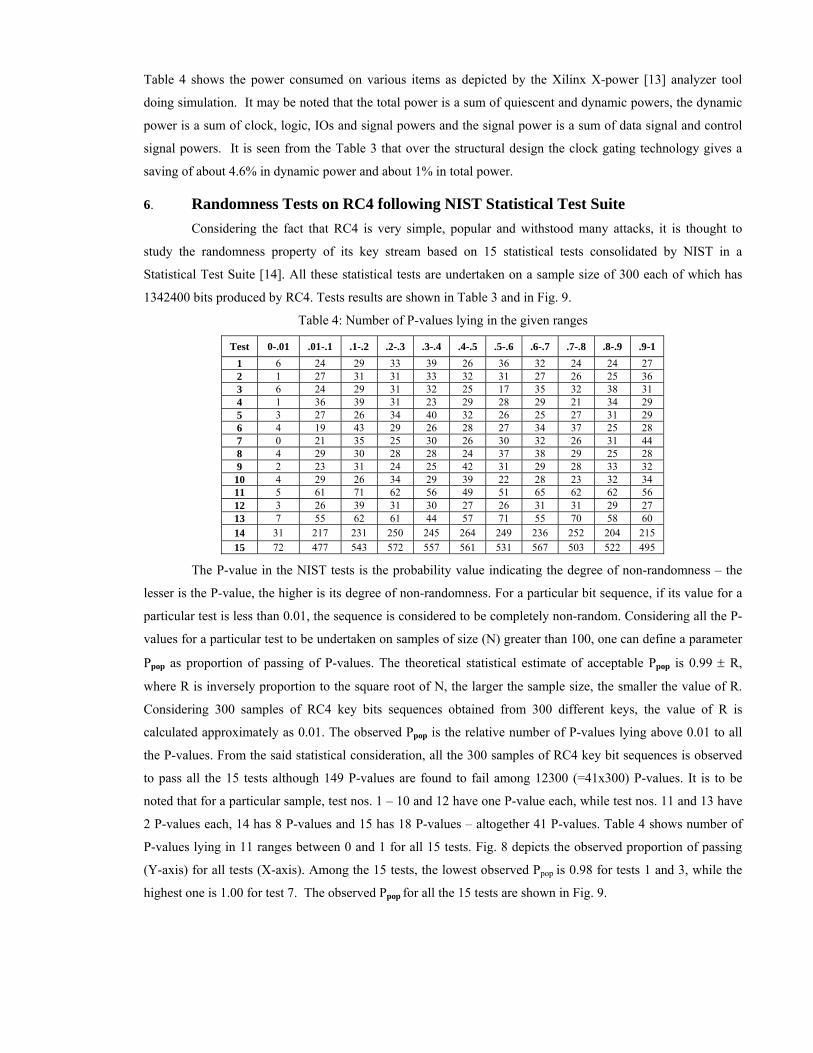
Table 4 shows the power consumed on various items as depicted by the Xilinx X-power [13] analyzer tool
doing simulation. It may be noted that the total power is a sum of quiescent and dynamic powers, the dynamic
power is a sum of clock, logic, IOs and signal powers and the signal power is a sum of data signal and control
signal powers. It is seen from the Table 3 that over the structural design the clock gating technology gives a
saving of about 4.6% in dynamic power and about 1% in total power.
6. Randomness Tests on RC4 following NIST Statistical Test Suite Considering the fact that RC4 is very simple, popular and withstood many attacks, it is thought to
study the randomness property of its key stream based on 15 statistical tests consolidated by NIST in a
Statistical Test Suite [14]. All these statistical tests are undertaken on a sample size of 300 each of which has
1342400 bits produced by RC4. Tests results are shown in Table 3 and in Fig. 9.
Table 4: Number of P-values lying in the given ranges
Test 0-.01 .01-.1 .1-.2 .2-.3 .3-.4 .4-.5 .5-.6 .6-.7 .7-.8 .8-.9 .9-1 1 6 24 29 33 39 26 36 32 24 24 27 2 1 27 31 31 33 32 31 27 26 25 36 3 6 24 29 31 32 25 17 35 32 38 31 4 1 36 39 31 23 29 28 29 21 34 29 5 3 27 26 34 40 32 26 25 27 31 29 6 4 19 43 29 26 28 27 34 37 25 28 7 0 21 35 25 30 26 30 32 26 31 44 8 4 29 30 28 28 24 37 38 29 25 28 9 2 23 31 24 25 42 31 29 28 33 32 10 4 29 26 34 29 39 22 28 23 32 34 11 5 61 71 62 56 49 51 65 62 62 56 12 3 26 39 31 30 27 26 31 31 29 27 13 7 55 62 61 44 57 71 55 70 58 60 14 31 217 231 250 245 264 249 236 252 204 215 15 72 477 543 572 557 561 531 567 503 522 495
The P-value in the NIST tests is the probability value indicating the degree of non-randomness – the
lesser is the P-value, the higher is its degree of non-randomness. For a particular bit sequence, if its value for a
particular test is less than 0.01, the sequence is considered to be completely non-random. Considering all the P-
values for a particular test to be undertaken on samples of size (N) greater than 100, one can define a parameter
Ppop as proportion of passing of P-values. The theoretical statistical estimate of acceptable Ppop is 0.99 ± R,
where R is inversely proportion to the square root of N, the larger the sample size, the smaller the value of R.
Considering 300 samples of RC4 key bits sequences obtained from 300 different keys, the value of R is
calculated approximately as 0.01. The observed Ppop is the relative number of P-values lying above 0.01 to all
the P-values. From the said statistical consideration, all the 300 samples of RC4 key bit sequences is observed
to pass all the 15 tests although 149 P-values are found to fail among 12300 (=41x300) P-values. It is to be
noted that for a particular sample, test nos. 1 – 10 and 12 have one P-value each, while test nos. 11 and 13 have
2 P-values each, 14 has 8 P-values and 15 has 18 P-values – altogether 41 P-values. Table 4 shows number of
P-values lying in 11 ranges between 0 and 1 for all 15 tests. Fig. 8 depicts the observed proportion of passing
(Y-axis) for all tests (X-axis). Among the 15 tests, the lowest observed Ppop is 0.98 for tests 1 and 3, while the
highest one is 1.00 for test 7. The observed Ppop for all the 15 tests are shown in Fig. 9.
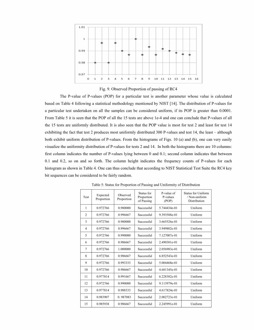
Fig. 9. Observed Proportion of passing of RC4
The P-value of P-values (POP) for a particular test is another parameter whose value is calculated
based on Table 4 following a statistical methodology mentioned by NIST [14]. The distribution of P-values for
a particular test undertaken on all the samples can be considered uniform, if its POP is greater than 0.0001.
From Table 5 it is seen that the POP of all the 15 tests are above 1e-4 and one can conclude that P-values of all
the 15 tests are uniformly distributed. It is also seen that the POP value is most for test 2 and least for test 14
exhibiting the fact that test 2 produces most uniformly distributed 300 P-values and test 14, the least – although
both exhibit uniform distribution of P-values. From the histograms of Figs. 10 (a) and (b), one can very easily
visualize the uniformity distribution of P-values for tests 2 and 14. In both the histograms there are 10 columns:
first column indicates the number of P-values lying between 0 and 0.1; second column indicates that between
0.1 and 0.2, so on and so forth. The column height indicates the frequency counts of P-values for each
histogram as shown in Table 4. One can thus conclude that according to NIST Statistical Test Suite the RC4 key
bit sequences can be considered to be fairly random.
Table 5: Status for Proportion of Passing and Uniformity of Distribution
Test Expected Proportion
Observed Proportion
Status for Proportion of Passing
P-value of P-values (POP)
Status for Uniform / Non-uniform
Distribution
1 0.972766 0.980000 Successful 5.744434e-01 Uniform
2 0.972766 0.996667 Successful 9.393588e-01 Uniform
3 0.972766 0.980000 Successful 3.665526e-01 Uniform
4 0.972766 0.996667 Successful 3.949802e-01 Uniform
5 0.972766 0.990000 Successful 7.127007e-01 Uniform
6 0.972766 0.986667 Successful 2.490301e-01 Uniform
7 0.972766 1.000000 Successful 2.056983e-01 Uniform
8 0.972766 0.986667 Successful 6.852543e-01 Uniform
9 0.972766 0.993333 Successful 5.004468e-01 Uniform
10 0.972766 0.986667 Successful 4.681345e-01 Uniform
11 0.977814 0.991667 Successful 6.228382e-01 Uniform
12 0.972766 0.990000 Successful 9.113979e-01 Uniform
13 0.977814 0.988333 Successful 4.617824e-01 Uniform
14 0.983907 0. 987083 Successful 2.002723e-01 Uniform
15 0.985938 0.986667 Successful 2.245991e-01 Uniform
(a) (b)
Fig.. 10. Uniformity Distribution of P-values of (a) Test 2 and (b) Test 14.
7. Conclusion The proposed 1-byte-1-clock RC4 design in FPGA is a coprocessor based design functioning in
parallel with a main processor. The encryption engine of the design implemented in one board successfully
communicates through its Ethernet port to another board containing the decryption engine. The present 1-byte
1-clock processing exploits conventional VHDL features and circuit-wise it is much simpler than the processing
of 2-bytes together in 2 clocks [1], leading to a throughput little better than that presented in [1, 11]. The clock
gating technology incorporated in the structural design is found to reduce dynamic power by about 5%. From
the statistical randomness studies, RC4 is found to be producing reasonably fair random key bit sequences.
8. References [1] S. Sen Gupta, K. Sinha, S. Maitra, and B. P. Sinha, “One Byte per Clock: A Novel RC4 Hardware”, Proc.
of Indocrypt 2010, pp. 347–363. [2] P. Kitsos, G. Kostopoulos, N. Sklavos and O. Koufopavlou., “Hardware Implementation of the RC4 stream
Cipher”, In Proc. of 46th IEEE Midwest Symposium on Circuits & Systems ’03, Cairo, Egypt, 2003. [3] D.P.Matthews Jr. “System and method for a fast hardware implementation of RC4”, US Patent No.
6549622, Campbell, CA, April, 2003. [4] S.Paul and B.Preneel, “A New weakness in the RC4 Key Stream Generator and an approach to improve the
security of the cipher”, Fast Software Encryption, Lecture Notes in Computer Science, LNCS 3017, Springer, Berlin, 2004, pp.245–259.
[5] S. Maitra and G. Paul, “Analysis of RC4 and proposal of additional layers for better security margin”, Indocrypt 2008, LNCS 5365, pp. 27–39, 2008.
[6] T. Good and M. Benaissa, "Hardware results for selected Stream Cipher candidates", sasc. crypto.rub.de/files/ sasc2007_191.pdf
[7] P. Leglise, FX. Standaert, G.Rouvroyand J. Quisquater, "Efficient implementation of recent stream ciphers on reconfigurable hardware devices", Proc. of the 26th Symposium on Information Theory in the Benelux”, Benelux (May 19-20, 2005), pp. 261 – 268.
[8] M. Galanis, P. Kitsos, G. Kostopoulos, N. Sklavos and C. Goutis, “Comparison of the Hardware Implementation of stream ciphers”, Int. Arab J. of Information Technology, Vol 2, No. 4, pp. 267 – 274, 2005.
[9] P. Leglise, F. Standaert, G. Rouvroy, J. Quisquater, “Efficient Implementation of Recent Stream Ciphers on Reconfigurable Hardware Devices”, Proc. of the 26th Symposium on Information Theory in the Benelux”, Benelux, May 19-20, 2005.
[10] M. Galanis, P. Kitos, G. Kostopoulos, N. Sklavos, O. Koufopavlou and C. Goutis, "Comparison of the hardware architectures and FPGA implementation of stream ciphers", Proc. Int. Conf. on Electronics, Circuits and Systems (ICECS 2004), pp. 571 - 574, IEEE March 2005.
[11] D.P.Matthews Jr., “Methods and apparatus for accelerating ARC4 processing”, US Patent No.7403615, Morgan Hill, CA, July, 2008.
[12] http://www.xilinx.com/tools/microblaze.htm [13] http://www.xilinx.com/support/documentation/sw_manuals/xilinx11/ug733.pdf [14] A Statistical Test Suite for Random and Pseudorandom Number Generators for Cryptographic
Applications, NIST, April 2010.