A Shimadzu Group Company Kratos AXIS Ultra DLD The small spot, parallel imaging, multi-technique...
136
A Shimadzu Group A Shimadzu Group Company Company www.kratos.com Kratos AXIS Ultra DLD The small spot, parallel imaging, multi-technique photoelectron spectrometer Dr Chris Blomfield Applications of high resolution XPS & AES
-
Upload
arleen-harmon -
Category
Documents
-
view
220 -
download
2
Transcript of A Shimadzu Group Company Kratos AXIS Ultra DLD The small spot, parallel imaging, multi-technique...

A Shimadzu Group CompanyA Shimadzu Group Company
www.kratos.com
Kratos AXIS UltraDLD
The small spot, parallel imaging, multi-technique photoelectron spectrometer
Dr Chris Blomfield
Applications of high resolution XPS & AES

A Shimadzu Group CompanyA Shimadzu Group Company
2
Kratos Analytical Ltd
Kratos headquarters Manchester UKservice/sales centresNew York, Tokyo,Singapore, Frankfurt

A Shimadzu Group CompanyA Shimadzu Group Company
3

A Shimadzu Group CompanyA Shimadzu Group Company
4
• ES-100 launched 1969• XSAM series 1980-90• Axis series launched 1995
– Axis HS 3 detectors 35– Axsi HSi 5 detectors40– Axis 165 8 detectors 45– Axis Ultra imaging 195– Axis Nova 40
Total units 355
All featuring common Axis technology– Virtual probe– Magnetic lens– Coaxial charge neutraliser– Spectral resolution and sensitivity
19
69
ES-100 ES-200 ES-
300
XSAM series HS
19
84
20
04
AXIS NovaAXIS UltraDLD
20
03
AXIS Ultra
19
97
AXIS 165
19
94
AXIS HSi
19
91

A Shimadzu Group CompanyA Shimadzu Group Company
5
What is the surface?
• What happens at surfaces is extremely important in a vast range of applications from environmental corrosion to medical implants.
• A surface can be thought of as the interface between different phases (solid, liquid or gas).
• We can think of the surface as the top layer of atoms but in reality the state of this layer is very much influenced by the 2 – 10 atomic layers below it (~0.5 – 3 nm).
• Surface modification treatments are often in the range of 10 – 100 nm thick. >100 nm can be thought of as the bulk.
• Surface analysis encompasses techniques which probe the properties in all these ranges.
A Shimadzu Group CompanyA Shimadzu Group Company
6
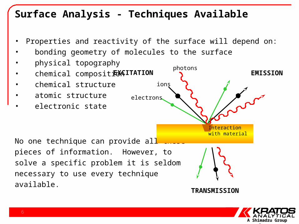
• Properties and reactivity of the surface will depend on:
• bonding geometry of molecules to the surface
• physical topography
• chemical composition
• chemical structure
• atomic structure
• electronic state
No one technique can provide all these
pieces of information. However, to
solve a specific problem it is seldom
necessary to use every technique
available.
photons
ions
electrons
EMISSION
TRANSMISSION
Interaction with material
EXCITATION
Surface Analysis - Techniques Available
A Shimadzu Group CompanyA Shimadzu Group Company
7
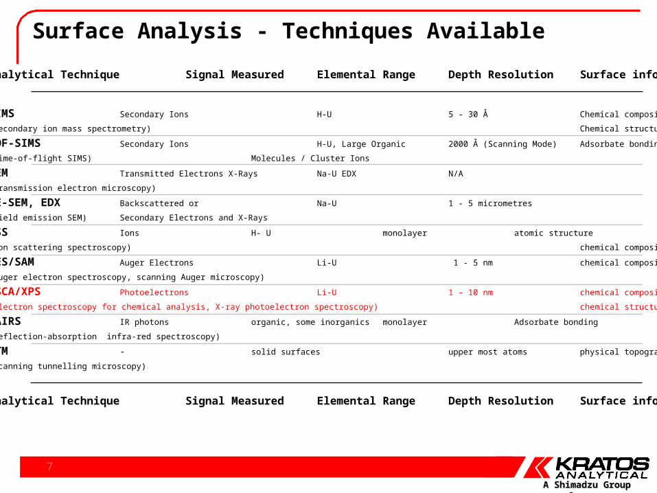
Analytical Technique Signal Measured Elemental Range Depth Resolution Surface info.
SIMS Secondary Ions H-U 5 - 30 Å Chemical composition
(secondary ion mass spectrometry) Chemical structure
TOF-SIMS Secondary Ions H-U, Large Organic 2000 Å (Scanning Mode) Adsorbate bonding
(time-of-flight SIMS) Molecules / Cluster Ions
TEM Transmitted Electrons X-Rays Na-U EDX N/A
(transmission electron microscopy)
FE-SEM, EDX Backscattered or Na-U 1 - 5 micrometres
(field emission SEM) Secondary Electrons and X-Rays
ISS Ions H- U monolayer atomic structure
(ion scattering spectroscopy) chemical composition
AES/SAM Auger Electrons Li-U 1 - 5 nm chemical composition
(Auger electron spectroscopy, scanning Auger microscopy)
ESCA/XPS Photoelectrons Li-U 1 – 10 nm chemical composition
(electron spectroscopy for chemical analysis, X-ray photoelectron spectroscopy) chemical structure
RAIRS IR photons organic, some inorganics monolayer Adsorbate bonding
(reflection-absorption infra-red spectroscopy)
STM - solid surfaces upper most atoms physical topography
(scanning tunnelling microscopy)
Analytical Technique Signal Measured Elemental Range Depth Resolution Surface info,
Surface Analysis - Techniques Available

A Shimadzu Group CompanyA Shimadzu Group Company
8
Surface Analysis - Techniques Available
A Shimadzu Group CompanyA Shimadzu Group Company
9
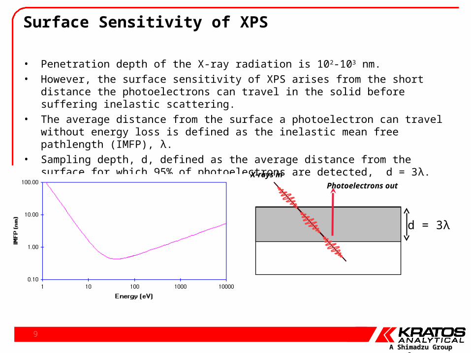
Surface Sensitivity of XPS
• Penetration depth of the X-ray radiation is 102-103 nm.• However, the surface sensitivity of XPS arises from the short distance the photoelectrons
can travel in the solid before suffering inelastic scattering. • The average distance from the surface a photoelectron can travel without energy loss is
defined as the inelastic mean free pathlength (IMFP), λ.• Sampling depth, d, defined as the average distance from the surface for which 95% of
photoelectrons are detected, d = 3λ.
dPhotoelectrons out
X-rays in
d = 3λ

A Shimadzu Group CompanyA Shimadzu Group Company
10
What information do we get from XPS?
• Surface sensitivity - photoelectron signal from first 1-10 layers of atoms and molecules.
• Identification of all elements (except H & He) at concentrations >0.1atomic%*.
• Quantitative determination of the elemental composition.• Information about the chemical state (molecular environment)
of the element.• Non-destructive analysis, including depth profiles, from the top
10 nm.• Destructive depth profiles of inorganic materials for 100s of nm.• Lateral variations in surface composition at >3µm resolution.• ‘Finger printing’ of materials using valance band.
• *Sensitivity - a sample with a surface of size 1 cm2 - this will have ca. 1015 atoms in the surface layer. In order to detect the presence of impurity atoms present at the 1% level, a technique must be sensitive to ca. 10 13 atoms. Contrast this with a spectroscopic technique used to analyse a 1 cm3 bulk liquid sample i.e. a sample of ca. 1022 molecules. The detection of 1013 molecules in this sample would require 1 ppb (one part-per-billion) sensitivity - very few techniques can provide anything like this level of sensitivity.

A Shimadzu Group CompanyA Shimadzu Group Company
11
The X-ray Photoelectron Spectroscopy Experiment
• Prof. Kai Siegbahn, Uppsala University, pioneered the technique of XPS, producing the first well defined spectrum in 1954 & was awarded a Noble prize for his work in 1981.
• Since then the basic building blocks of the X-ray photoelectron spectrometer have not changed.
• However, UHV technology and electronics have improved!
X-ray source
UHV analysischamber
Electron energy analyser
Electron detector
sample

A Shimadzu Group CompanyA Shimadzu Group Company
12
The Photoelectron Spectrum – Surveys/Wide ScansWhich elements are present and how much have we got?
Cu 2p
O KLL Auger
O 1s
N 1s
C 1s
Cu LMM Auger
Cu 3p
Cu 3sCl 2p
Cl 2s
• The energy of the photoelectron peak is indicative of the element from which it originated.
• The number of electrons (peak area) is related to the elemental concentration.
• Both photoemission and Auger peaks observed in a spectrum.
• Peaks are superimposed on a rising background, due to inelastically scattered photoelectrons.

A Shimadzu Group CompanyA Shimadzu Group Company
13
O 1s
C 1s
O KLLAuger
O 1s C 1s
The Photoelectron Spectrum – High ResolutionWhat chemical state are the elements in?
High resolution spectra show the subtle shifts
in energy of photoelectrons originating form
different chemical environments.
A Shimadzu Group CompanyA Shimadzu Group Company
14
Chemical State Information
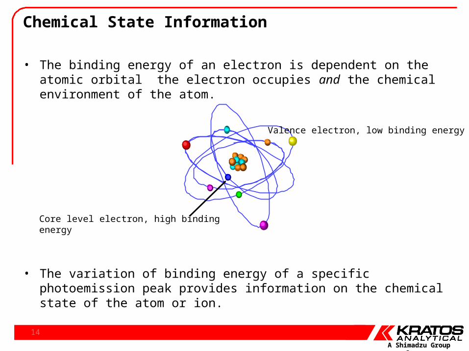
• The binding energy of an electron is dependent on the atomic orbital the electron occupies and the chemical environment of the atom.
• The variation of binding energy of a specific photoemission peak provides information on the chemical state of the atom or ion.
Core level electron, high binding energy
Valence electron, low binding energy

A Shimadzu Group CompanyA Shimadzu Group Company
15
Chemical State Information
• Typical binding energies for C 1s photoemission peaks from organic materials
• functional group binding energy (eV)
• hydrocarbon C-H, C-C 285.0• amine C-N 286.0• alcohol, ether C-O-H, C-O-C 286.5• fluorocarbon C-F 287.8• carbonyl C=O 288.0• 2F bound to a carbon -CH2CF2- 290.6• 3F bound to a carbon -CF3 293-294
• Typical chemical shifts for O 1s photoemission peaks from organic materials
• functional group binding energy (eV)
• carbonyl -C=O, O-C=O 532.2• alcohol, ether -O-H, O-C-O 532.8• ester C-O-C=O 533.7
A Shimadzu Group CompanyA Shimadzu Group Company
16
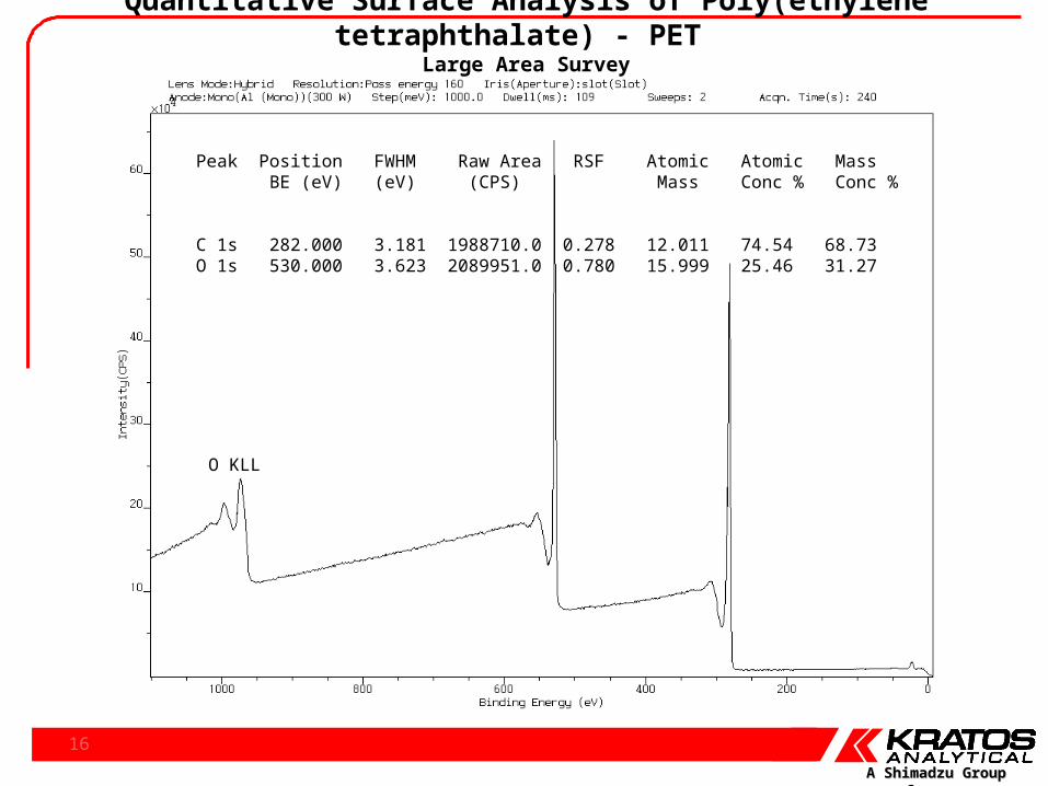
Quantitative Surface Analysis of Poly(ethylene tetraphthalate) - PET Large Area Survey
O KLL
Peak Position FWHM Raw Area RSF Atomic Atomic Mass BE (eV) (eV) (CPS) Mass Conc % Conc % C 1s 282.000 3.181 1988710.0 0.278 12.011 74.54 68.73 O 1s 530.000 3.623 2089951.0 0.780 15.999 25.46 31.27
A Shimadzu Group CompanyA Shimadzu Group Company
17
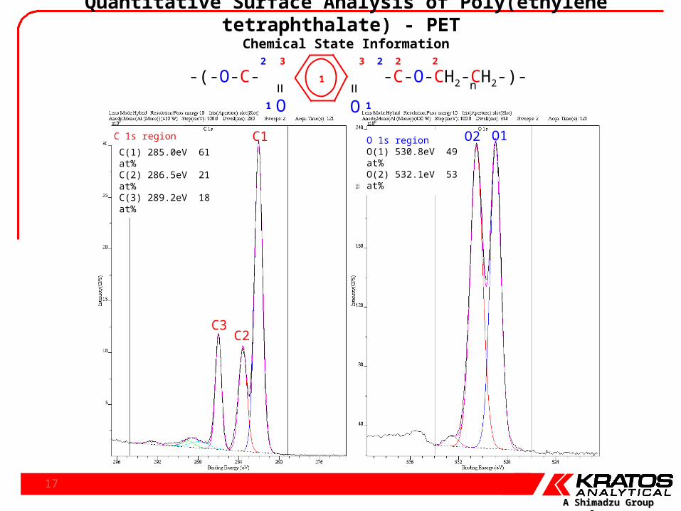
Quantitative Surface Analysis of Poly(ethylene tetraphthalate) - PET Chemical State Information
C 1s region O 1s regionO(1) 530.8eV 49 at% O(2) 532.1eV 53 at%
C(1) 285.0eV 61 at%C(2) 286.5eV 21 at%C(3) 289.2eV 18 at%
C3C2
C1 O1O2
-(-O-C- -C-O-CH2-CH2-)-= =
O On
2223
1
32
1
1

A Shimadzu Group CompanyA Shimadzu Group Company
18
Monochromated vs non-monochromated X-ray source
Monochromated Al Kα excited Ag spectrum
Non-monochromated Mg Kα excited Ag spectrum
FWHM 0.97 eV
FWHM 0.46 eV
satellite
Things to note: loss of rising background, narrower peaks, loss of satellite peaks, movement of Auger peaks
Ag 3d
Ag 3p3/2
Ag 3p1/2
Ag 3p3/2Ag 3p1/2
Ag 3d5/2
Ag 3d3/2
Ag 3d5/2
Ag 3d3/2Ag 3d
Ag 3s
Ag 3s
Ag MNV Auger
satellite

A Shimadzu Group CompanyA Shimadzu Group Company
19
Beyond Large Area Spectroscopy
thin film
<10 nm
thicker layer or multilayers heterogeneous surface
angle resolved XPS depth profile parallel imaging selected area spectroscopy
A Shimadzu Group CompanyA Shimadzu Group Company
20
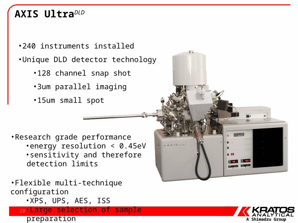
AXIS UltraDLD
•Research grade performance•energy resolution < 0.45eV•sensitivity and therefore detection limits
•Flexible multi-technique configuration•XPS, UPS, AES, ISS•Large selection of sample preparation
•240 instruments installed
•Unique DLD detector technology
•128 channel snap shot
•3um parallel imaging
•15um small spot

A Shimadzu Group CompanyA Shimadzu Group Company
21
Axis Ultra performance
1.0E+03
1.0E+04
1.0E+05
1.0E+06
1.0E+07
0.4 0.5 0.6 0.7 0.8 0.9 1 1.1 1.2 1.3
Resolution (eV)
Sen
siti
vity
(cp
s)
Hybrid 110um 55um 27um
5eV
40eV
10eV
20eV
80eV

A Shimadzu Group CompanyA Shimadzu Group Company
22
Instrument overview
1 Al monochromatic source2 Mg/Al achromatic source3 Low energy floating ion gun4 165mm radius HSA & SMA5 Transfer lens & aperture/iris6 TMP 250 l/s for STC
Options
7 10 kV Field emission source8 UPS lamp
1.2.3.
4.
5.
6.
8.7.

A Shimadzu Group CompanyA Shimadzu Group Company
23
Configuration
1 Al monochromatic source2 Mg/Al achromatic source3 Low energy floating ion gun4 CCTV camera port (not shown)5 Magnetic lens6 Ion pump offset from SAC7 TMP 250 l/s for STC
Options
8 10 kV Field emission source9 UPS lamp
1.
2.
3.
4.
6.
5.
7.
8.
9.

A Shimadzu Group CompanyA Shimadzu Group Company
24
Si 2p Spectrum – pass energy 5 eV
FWHM Si 2p3/2 0.367 eV
Peak height 5403 cpsPeak fitted spectrum Si 2p3/2
Si 2p1/2
oxides
Native oxide

A Shimadzu Group CompanyA Shimadzu Group Company
25
Large area (700 x 300 microns) Ag 3d5/2 Fermi Edge spectrum recorded at 5 eV pass energy and 600 W X-ray power.
16% - 84% Edge resolution = 0.233 eV
Ag Fermi edge - RT – pass energy 5 eV
Ag EF < 250meV

A Shimadzu Group CompanyA Shimadzu Group Company
26
Ag 3d5/2 peak resolution (FWHM) = 0.445 eV, ~250KCPS
Ag 3d5/2 – pass energy 5 eV
A Shimadzu Group CompanyA Shimadzu Group Company
www.kratos.com
High sensitivity means high detection limits or fast analysis time

A Shimadzu Group CompanyA Shimadzu Group Company
28
Typical high sensitivity available
• Improved detection limits <0.05% allow analysis of low concentrations of elements
– Al-Zn-In anodes are used to protect marine steel structures from corrosion.
– study with XPS of the active In element – reveals surface segregation to a maximum of 4% over 1 year
exposure

A Shimadzu Group CompanyA Shimadzu Group Company
29
Overlap with Ca 2s
In 3d3/2 used for quantification
Low concentration In 3d quantification

A Shimadzu Group CompanyA Shimadzu Group Company
30
XPS shows surface concentration of In during corrosion
• Cut anode surface used to represent bulk– XPS In 0.02wt%
– GDOES In 0.0185wt%
• As cast anode surface ~1wt% In• Corrosion tests show an increase to 4wt% over 1 year
simulated corrosion

A Shimadzu Group CompanyA Shimadzu Group Company
www.kratos.com
Analysis of insulators

A Shimadzu Group CompanyA Shimadzu Group Company
32
Origin of Charge Neutralisation Electrons
Magnetic Lens Pole Piece
(2) Charge balance plate (-ve potential)
(1) Filament
(3) Low Energy Electron Trajectory in the Magnetic Field
Sample
1) Electrons are thermionically emitted from the charge neutraliser filament.
2) Negative potential of the charge balance plate forces the charge neutralisation electrons towards the sample. There is no direct line of sight of the filament with the sample.
3) The low energy electrons are confined by the magnetic field of the magnetic immersion lens, following an oscillating path between sample and charge balance plate.
4) As sample develops a positive charge, charge neutralisation electrons are attracted to the surface.

A Shimadzu Group CompanyA Shimadzu Group Company
33
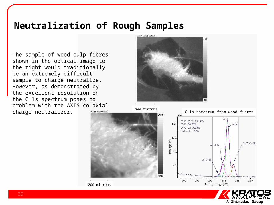
200 microns
800 micronsC 1s spectrum from wood fibres
Neutralisation of Rough Samples
The sample of wood pulp fibres shown in the optical image to the right would traditionally be an extremely difficult sample to charge neutralise. However, as demonstrated by the excellent resolution on the C 1s spectrum poses no problem with the AXIS co-axial charge neutraliser.

A Shimadzu Group CompanyA Shimadzu Group Company
34
Charge Neutralization
•Fully automatic system standard parameter for 99% of samples
•Simple software electron only source
•No Ar* ions
•Works on topographic samples
There are only three parameters to define for the charge neutralisation system.
Normal user operation of neutraliser

A Shimadzu Group CompanyA Shimadzu Group Company
35
Neutralization of Rough Samples
+++++
++++
+++
rough sample surface
Kratos neutralisation system - electrons following a spiral path
Collimated electrons or ions from a low energy electron/ion source
For a rough sample, parts of the surface may be shadowed from neutralisation electrons originating from a collimated electron gun so that the sample will only be partially neutralised. This is overcome by the Kratos charge neutralisation system, where the low energy electrons reach the sample from all directions as a result of their spiral trajectory
A Shimadzu Group CompanyA Shimadzu Group Company
36
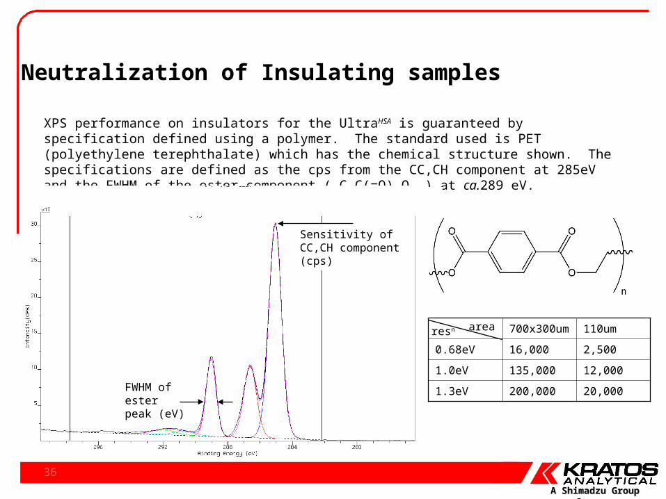
Neutralization of Insulating samples
XPS performance on insulators for the UltraHSA is guaranteed by specification defined using a polymer. The standard used is PET (polyethylene terephthalate) which has the chemical structure shown. The specifications are defined as the cps from the CC,CH component at 285eV and the FWHM of the ester component ( C-C(=O)-O- ) at ca.289 eV.
700x300um 110um
0.68eV 16,000 2,500
1.0eV 135,000 12,000
1.3eV 200,000 20,000
resn area
Sensitivity of CC,CH component (cps)
FWHM of ester peak (eV)
A Shimadzu Group CompanyA Shimadzu Group Company
37
0
50000
100000
150000
200000
250000
300000
350000
400000
450000
0.6 0.7 0.8 0.9 1 1.1 1.2 1.3 1.4
FWHM O=C-O (eV)
Sen
siti
vity
C-H
(cp
s)
Measured Spec
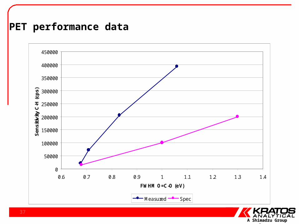
PET performance data

A Shimadzu Group CompanyA Shimadzu Group Company
38
10 eV PE FWHM = 0.68eV
40eV PE FWHM = 0.83 eV
Clear loss of chemical resolution evidenced in carbonyl peak
Effect of PE on measured data
A Shimadzu Group CompanyA Shimadzu Group Company
39
200 microns
800 micronsC 1s spectrum from wood fibres
Neutralization of Rough Samples
The sample of wood pulp fibres shown in the optical image to the right would traditionally be an extremely difficult sample to charge neutralize. However, as demonstrated by the excellent resolution on the C 1s spectrum poses no problem with the AXIS co-axial charge neutralizer.
A Shimadzu Group CompanyA Shimadzu Group Company
40
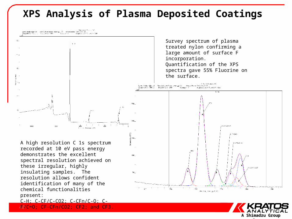
XPS Analysis of Plasma Deposited Coatings
Survey spectrum of plasma treated nylon confirming a large amount of surface F incorporation. Quantification of the XPS spectra gave 55% Fluorine on the surface.
A high resolution C 1s spectrum recorded at 10 eV pass energy demonstrates the excellent spectral resolution achieved on these irregular, highly insulating samples. The resolution allows confident identification of many of the chemical functionalities present: C-H; C-CF/C-CO2; C-CFn/C-O; C-F/C=O; CF-CFn/CO2; CF2; and CF3.

A Shimadzu Group CompanyA Shimadzu Group Company
41
XPS Analysis of Plasma Deposited Coatings
High resolution C 1s spectrum of wet chemical fluorosolvent treated nylon after 1 wash and 5 washes demonstrating loss of surface coating
Overlay of C 1s spectra recorded from the wet chemical fluorosolvent treated fabric before washing, after 5 washes and after 5 washes and ironing.
Wet chemical treatment
5 Washes
5 washes + ironing

A Shimadzu Group CompanyA Shimadzu Group Company
www.kratos.com
Small area analysis

A Shimadzu Group CompanyA Shimadzu Group Company
43
The Selected Area Aperture

A Shimadzu Group CompanyA Shimadzu Group Company
44
Selected Area ApertureThe selected area aperture is used to define a small analysis area at the surface. There are two approaches that may be adopted to allow XPS analysis from areas in the micron range. One approach is ti insert an aperture into the electrostatic lens column, as shown in the figures below, to forma virtual probe at the surface. An alternative approach is to use a focussed excitation source with the transfer lens collecting photoelectrons from the irradiated area. Selected area spectroscopy and mapping is descried in greater detail in technical note MO224 (available from Kratos Analytical).
110m analysis area 27m analysis area
Selected area apertures
Angle defining iris
Analyser entrance slit
Ele
ctro
stat
ic le
ns c
olum
n
Ele
ctro
stat
ic le
ns c
olum
n
A Shimadzu Group CompanyA Shimadzu Group Company
45
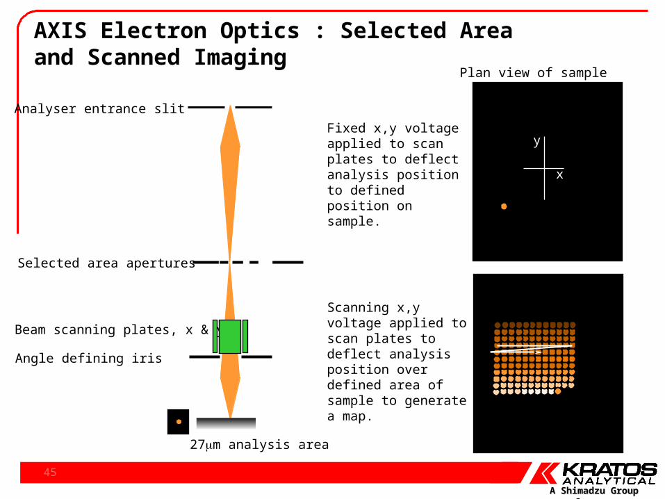
AXIS Electron Optics : Selected Area and Scanned Imaging
x
yFixed x,y voltage applied to scan plates to deflect analysis position to defined position on sample.
Scanning x,y voltage applied to scan plates to deflect analysis position over defined area of sample to generate a map.
Selected area apertures
Angle defining iris
Analyser entrance slit
Beam scanning plates, x & y
27m analysis area
Plan view of sample

A Shimadzu Group CompanyA Shimadzu Group Company
46
Plasma modification and Patterning
• Substrate : Polystyrene with surface modified by exposure to CFx containing plasma.
• TEM grid then used as a mask and sample reintroduced into a plasma chamber.
• Substrate and grid exposed to C-O, C-N containing plasma.
• Can pattern be observed?• What further information can be extracted from the images?
PSC-O,C-Nfunctional groups
PSCFx
functional groups

A Shimadzu Group CompanyA Shimadzu Group Company
47
Plasma modification and Patterning
- Large area (300x700um) survey scan from patterned area
F 1s
O 1s
N 1s
C 1s
- F 1s parallel image for 60 sec.
As the sample was a clear polymer sheet with thin plasma modified layer there was nothing to see optically.
A large area (300x700um) survey spectrum acquired from the sample showed photoelectron peaks from fluorine, oxygen, nitrogen and carbon.
A quick parallel image corresponding to the fluorine gave a well resolved grid pattern.
To better characterise the chemistry of the surface small spot spectra were acquired.

A Shimadzu Group CompanyA Shimadzu Group Company
48
Defining the selected area spectrum position
The parallel image is used to define the position for the small spot spectra by simply clicking with the mouse and importing the position into the acquisition software shown to the right.
The virtual probe is deflected to the defined position using the beam scanning plates.
CF3
CF2
CC,CH
CO,CN
CC,CH
CO,CN

A Shimadzu Group CompanyA Shimadzu Group Company
www.kratos.com
Imaging XPS
A Shimadzu Group CompanyA Shimadzu Group Company
50
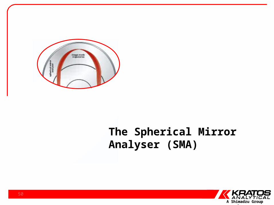
The Spherical Mirror Analyser (SMA)
A Shimadzu Group CompanyA Shimadzu Group Company
51
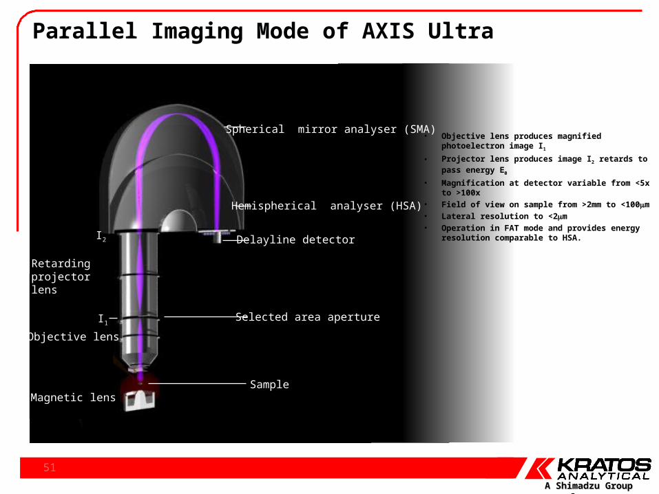
Parallel Imaging Mode of AXIS Ultra
Outer hemisphere of HSA
Charge neutraliser
Spherical mirror analyser (SMA)
Hemispherical analyser (HSA)
Magnetic lensSample
Selected area aperture
Objective lens
Delayline detector
Retarding projectorlens
• Objective lens produces magnified photoelectron image I1
• Projector lens produces image I2 retards to pass energy E0
• Magnification at detector variable from <5x to >100x
• Field of view on sample from >2mm to <100m
• Lateral resolution to <2m
• Operation in FAT mode and provides energy resolution comparable to HSA.
I1
I2
A Shimadzu Group CompanyA Shimadzu Group Company
52
SMA and Parallel Imaging
• Fast Parallel XPS Imaging• as the sample is moved, so the photoelectron image moves.
• Lateral Resolution specification < 3 m• Fixed analyser transmission (FAT) mode
• energy resolution constant at all binding energies.• good energy resolution at all binding energies.
• ‘Real time’ chemical state XPS imaging• ability to differentiate between elements in different chemical states.

A Shimadzu Group CompanyA Shimadzu Group Company
53
Variable Field of View - Real Time Imaging of Au grid
2 mm fov
400 m fov
200 m fov• Au images acquired in less than 60 secs.
• Field of view (f.o.v.) changed by selecting predefined lens modes for a specific magnification. The new f.o.v. is displayed within seconds.
800 m fov 400 m fov

A Shimadzu Group CompanyA Shimadzu Group Company
54
XPS Imaging of 5 m Cu Bars
2.2 m edge
25m from centre of bars
After acquisition of the image a line scan can be generated. The line-scan can be processed to provide edge measurements, giving an indication of lateral resolution
A Shimadzu Group CompanyA Shimadzu Group Company
55
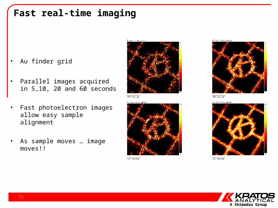
Fast real-time imaging
• Au finder grid
• Parallel images acquired in 5,10, 20 and 60 seconds
• Fast photoelectron images allow easy sample alignment
• As sample moves … image moves!!

A Shimadzu Group CompanyA Shimadzu Group Company
56
Large area fast parallel imaging
3.2 x 3.2mm image7um spatial resolution300 sec total acquisition time
1.6 x 1.6mm image3um spatial resolution300 sec total acquisition time
A Shimadzu Group CompanyA Shimadzu Group Company
57
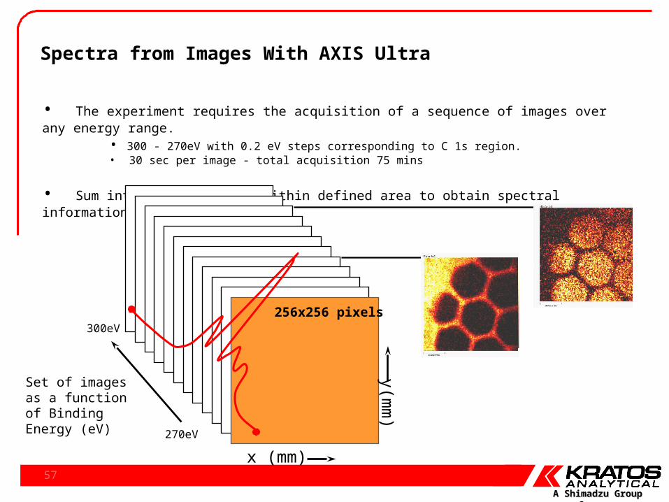
Spectra from Images With AXIS Ultra
• The experiment requires the acquisition of a sequence of images over any energy range.• 300 - 270eV with 0.2 eV steps corresponding to C 1s region.• 30 sec per image - total acquisition 75 mins
• Sum intensity of pixels within defined area to obtain spectral information form that area
Set of images as a function of Binding Energy (eV)
x (mm)
y(m
m)
256x256 pixels
270eV
300eV

A Shimadzu Group CompanyA Shimadzu Group Company
58
Spectra from images
As generatedspectrum generated from significant PCA components
It is possible to use the image dataset to reconstruct a spectrum. The example below shows a spectrum generated from a single pixel (blue) using the raw images. When the noise has been removed from the image dataset using the PCA approach a much more convincing spectrum is shown.
This spectrum was defined from a single pixel 1.4 x 1.4um area ! It is possible to generate a spectrum from any of the 256 x 256 pixels on the imaged area – over 65,500 spectra !!

A Shimadzu Group CompanyA Shimadzu Group Company
59
Spectra from Images
C 1s spectrum generated from 5x5 pixels
CC,CH
CO
C=O
-CF2
-CF3
• After generating spectrum from images it is then possible to deconvolute the data and fit with components.
• An image may then be generated corresponding to a specific component.
– Has the advantage that peak shifts may be accommodated in by the model.
– Integrating area under the peak allows chemical state images show relative concentrations.

A Shimadzu Group CompanyA Shimadzu Group Company
60
Quantitative Elemental and Chemical State Imaging
CH, CC CO, CN C=O CF2
-CF3 Fluorine Nitrogen Oxygen

A Shimadzu Group CompanyA Shimadzu Group Company
www.kratos.com
Large area imaging – image stitching

A Shimadzu Group CompanyA Shimadzu Group Company
62
glass
ZTO (ZnSnO)
CTO (CdSnO)
CdSCdTe
Approximate thickeness / nm
2020
1000-350
1000-350
CdTe / CdS / ZTO / CTO / glass stack
XPS imaging used for film continuity

A Shimadzu Group CompanyA Shimadzu Group Company
63
100 m
In photoelectron image90 sec acquisition
Na photoelectron image240 sec acquisition
100 m
NREL CIGS Sample : XPS images

A Shimadzu Group CompanyA Shimadzu Group Company
64
1mm
1mm
In XPS image(9x4) stitch
Na XPS image(9x4) stitch
NREL CIGS Sample : XPS stitched images

A Shimadzu Group CompanyA Shimadzu Group Company
65
NREL CIGS Sample : XPS stitched images
Overlay of In (9x4) stitched image (red) and Na (9x4) stitched image (blue)
A Shimadzu Group CompanyA Shimadzu Group Company
66
Na
1s
Cu
2p
O K
LL
In M
NN
In 3
p
In 3
p
O 1
s
In 3
d
Na
KL
L
C 1
s
Se
3p
Se
LM
M
Se
3dN
a 2
s
Ga
3d /
In
4d
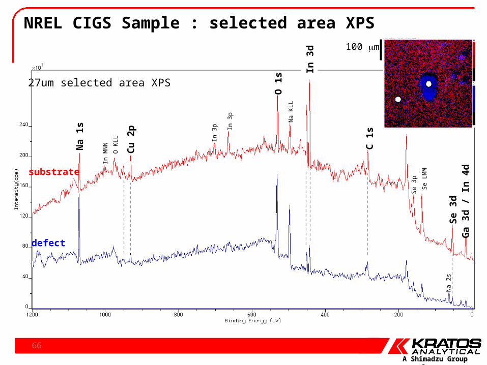
27um selected area XPS
100 m
defect
substrate
NREL CIGS Sample : selected area XPS
A Shimadzu Group CompanyA Shimadzu Group Company
www.kratos.com
Angle resolved XPS

A Shimadzu Group CompanyA Shimadzu Group Company
68
Angular Dependence of XPS
d
d ~ 8-10 nm
d
photoelectrons
X-rays
photoelectrons
X-rays

A Shimadzu Group CompanyA Shimadzu Group Company
69
Si wafer with native oxide
0° to sample normal
Bulk Sensitive
70° to sample normal
Surface Sensitive
Si oxide
Si Hydroxide
Si 2p1/2
Si 2p3/2
Si Bulk
Si OxideCarbon

A Shimadzu Group CompanyA Shimadzu Group Company
70
Native oxide on Si wafer
0
5
10
15
20
25
30
35
40
45
50
0 10 20 30 40 50 60 70 80
Angle (degree)
Ato
mic
Co
nce
ntr
atio
n (
%) O 1s
C 1s
Si Oxide
Si Metal
Si wafer with native oxide
• Si sample with native oxide was not cleaned prior to analysis.
• Sample tilted from 0° through 70° with steps of 10°
• The contribution from Si oxide and Si hydroxide convoluted components have been combined.

A Shimadzu Group CompanyA Shimadzu Group Company
71
MEMs Depth Profile Reconstruction for Si wafer with native oxide
MEMs - Reconstructed Depth Profile
0
10
20
30
40
50
60
70
80
90
100
0.0 0.5 1.0 1.5 2.0 2.5 3.0 3.5 4.0 4.5 5.0
Depth (nm)
Ato
mic
Co
nc
en
tra
tio
n (
%)
O 1s
C 1s
Si Oxide
Si Metal
0
20
40
60
80
100
120
0 1 2 3 4 5
Ato
mic
Co
nce
ntr
atio
n [
%]
Depth [nm]
Reconstructed depth profiles alfa =37.0392 c = 4.89436
Si MetalPrior:Si Metal

A Shimadzu Group CompanyA Shimadzu Group Company
72
Substrate Substrate
O
OO
OO
F
OO
O
OO
O F
OO
OO
O
OO
OO
S u b s t r a t eS u b s t r a t e
O
OO
OO
F
OO
O
OO
O F
OO
OO
O
OO
OO
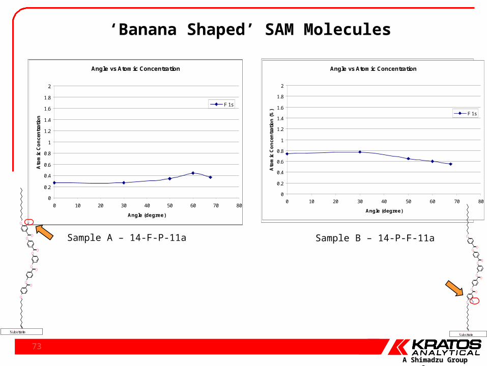
Sample A – 14-F-P-11a Sample B – 14-P-F-11a
• Chemical Formula – C59H69FO10
• HF used for the removal of native oxide on Si wafer.
• Hydrogen terminated Si-surface covalently reacts with alkene chain end to form strong Si-C bonds
• Detailed studies using AFM, water contact angle and ATR-FTIR techniques have shown that the monolayer is densely packed and well ordered.
‘Banana Shaped’ SAM Molecules
A Shimadzu Group CompanyA Shimadzu Group Company
73
Angle vs Concentration
0
10
20
30
40
50
60
0 10 20 30 40 50 60 70 80
Angle (degree)
Ato
mic
Co
nce
ntr
atio
n (
%)
F 1s
O 1s
C 1s
Si Oxide
Si Metal
Angle Vs. Concentration
0
10
20
30
40
50
60
70
0 10 20 30 40 50 60 70 80
Angle (degree)
Ato
mic
co
nce
ntr
atio
n (
%)
F 1s
O 1s
C 1s
Si Oxide
Si Metal
Sample A – 14-F-P-11a Sample B – 14-P-F-11a
Angle vs Atomic Concentration
0
0.2
0.4
0.6
0.8
1
1.2
1.4
1.6
1.8
2
0 10 20 30 40 50 60 70 80
Angle (degree)
Ato
mic
Co
nce
ntr
atio
n
F 1s
Angle vs Atomic Concentration
0
0.2
0.4
0.6
0.8
1
1.2
1.4
1.6
1.8
2
0 10 20 30 40 50 60 70 80
Angle (degree)
Ato
mic
Co
nce
ntr
atio
n (
%)
F 1s
Substrate
O
OO
OO
F
OO
O
OO
S u b s t r a t e
O
OO
OO
F
OO
O
OO
Substrate
O F
OO
OO
O
OO
OO
S u b s t r a t e
O F
OO
OO
O
OO
OO
‘Banana Shaped’ SAM Molecules

A Shimadzu Group CompanyA Shimadzu Group Company
74
MEMs Reconstructed Depth Profile
0.0
10.0
20.0
30.0
40.0
50.0
60.0
70.0
80.0
90.0
100.0
0 1 2 3 4 5 6 7 8 9 10
Depth (nm)
Ato
mic
Co
nce
ntr
atio
n (
%)
F 1s * 5
O 1s
C 1s
Si Oxide
Si Metal
MEMs Depth Profile Reconstruction – Sample A
Substrate
O
OO
OO
F
OO
O
OO
S u b s t r a t e
O
OO
OO
F
OO
O
OO

A Shimadzu Group CompanyA Shimadzu Group Company
75
MEMs Reconstructed Depth Profile
0.0
10.0
20.0
30.0
40.0
50.0
60.0
70.0
80.0
90.0
100.0
0 1 2 3 4 5 6 7 8 9 10
Depth (nm)
Ato
mic
Co
nce
ntr
atio
n (
%)
F 1s * 5
O 1s
C 1s
Si Oxide
Si Metal
MEMs Depth Profile Reconstruction – Sample B
Substrate
O F
OO
OO
O
OO
OO
S u b s t r a t e
O F
OO
OO
O
OO
OO

A Shimadzu Group CompanyA Shimadzu Group Company
76
MEMs Depth Profile Reconstruction
0
2
4
6
8
10
12
14
16
0 1 2 3 4 5 6 7 8 9 10
Depth (nm)
Ato
mic
Co
nc
en
tra
tio
n (
%)
Sample A *5
Sample B *5
Substrate
O F
OO
OO
O
OO
OO
S u b s t r a t e
O F
OO
OO
O
OO
OO
Sample A
Substrate
O
OO
OO
F
OO
O
OO
S u b s t r a t e
O
OO
OO
F
OO
O
OO
Sample B
MEMs Depth Profile Reconstruction – Depth Distribution of Fluorine

A Shimadzu Group CompanyA Shimadzu Group Company
77
XPS depth profiling - inorganics
• Accepted standard technique for analysis of inorganic samples• Improvements in small spot XPS mean small etch craters can be
used• Etch rates in the range of 1 – 50nm min-1 (Ta2O5)
• Recent advances in ion gun technology have lead to lower primary ion energies for improved interface resolution.
A Shimadzu Group CompanyA Shimadzu Group Company
78
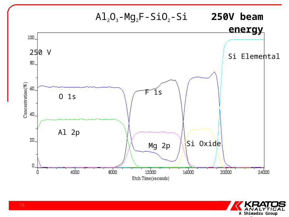
250 V
O 1s
Al 2p
F 1s
Mg 2p Si Oxide
Si Elemental
Al2O3-Mg2F-SiO2-Si 250V beam energy

A Shimadzu Group CompanyA Shimadzu Group Company
79
width of 1st Al layerfwhm 58nm
width of last Al layerfwhm 63nm
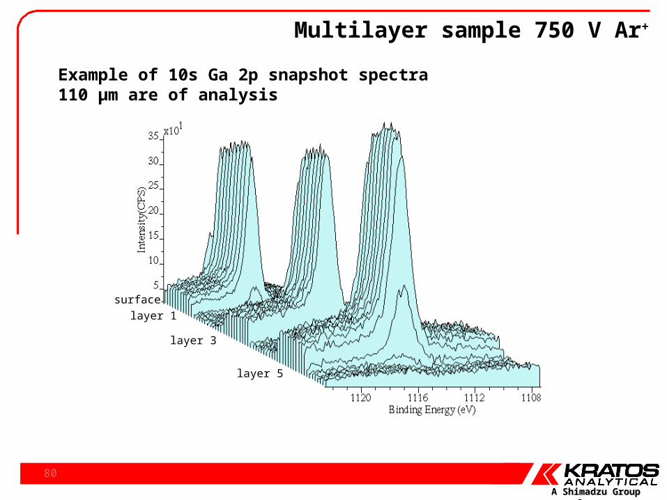
Multilayer sample 750 V Ar+Etch conditions: 750 V, 3 x 3 mm raster, 60 s etch cycles. Etch rate on Ta2O5: 2.3 nm/minAcquisition: 10 s snapshot spectra, cycle time 2min 50 sTotal acquisition time: ~14 hours
A Shimadzu Group CompanyA Shimadzu Group Company
80
surface
layer 1
layer 3
layer 5
Example of 10s Ga 2p snapshot spectra 110 µm are of analysis
Multilayer sample 750 V Ar+

A Shimadzu Group CompanyA Shimadzu Group Company
81
Si 2p region
Si (elemental)
Si (carbide)
Si (oxide)
Si 2p region
SiC/Si : high resolution snapshot spectra

A Shimadzu Group CompanyA Shimadzu Group Company
82
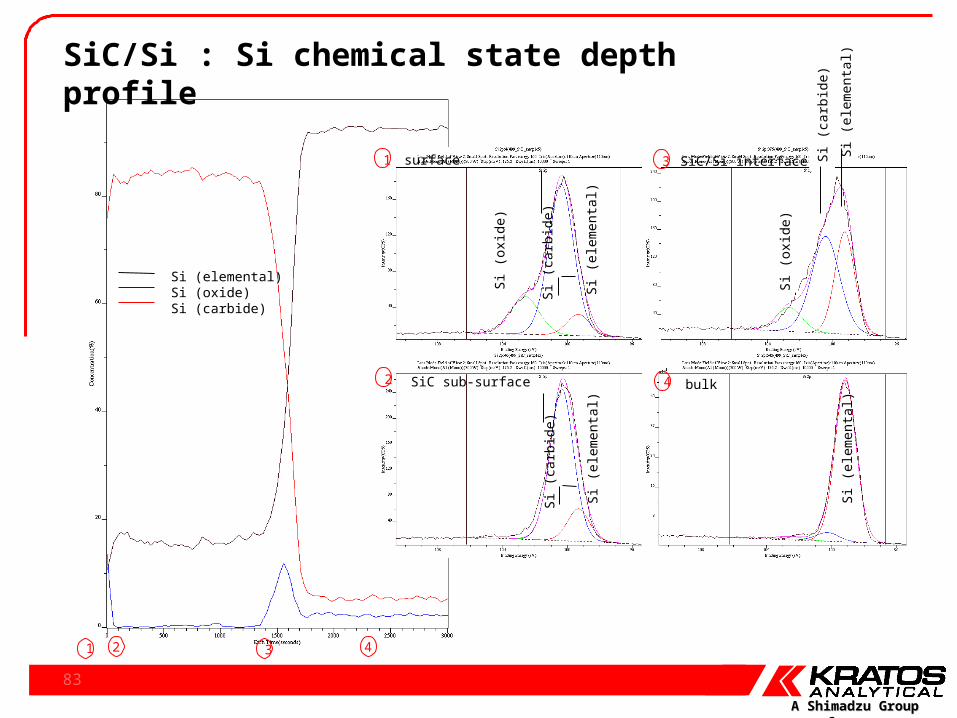
SiC/Si : Elemental depth profile
Oxygen
Silicon
Carbon
750 V Ar+ ions3x3mm rastered crater
A Shimadzu Group CompanyA Shimadzu Group Company
83
SiC/Si : Si chemical state depth profile
Si (
elem
enta
l)
Si (
carb
ide)
Si (
oxid
e)
Si (
elem
enta
l)
Si (
carb
ide)
Si (
oxid
e)
Si (
elem
enta
l)
Si (
elem
enta
l)
Si (
carb
ide)
2 41 3
1
2
3
4
Si (elemental)Si (oxide)Si (carbide)
surface
bulk
SiC/Si interface
SiC sub-surface

A Shimadzu Group CompanyA Shimadzu Group Company
www.kratos.com
Auger electron spectroscopy - AES

A Shimadzu Group CompanyA Shimadzu Group Company
85
FE-Auger Electron Source
Field emission electron source and ion pump shown here in situ on an AXIS Ultra.

A Shimadzu Group CompanyA Shimadzu Group Company
86
Hi Magnification SEM with Linescan
5 microns
266 nm resolution measured using 80% - 20% line scan from SiO2 / Si sample.
A Shimadzu Group CompanyA Shimadzu Group Company
87
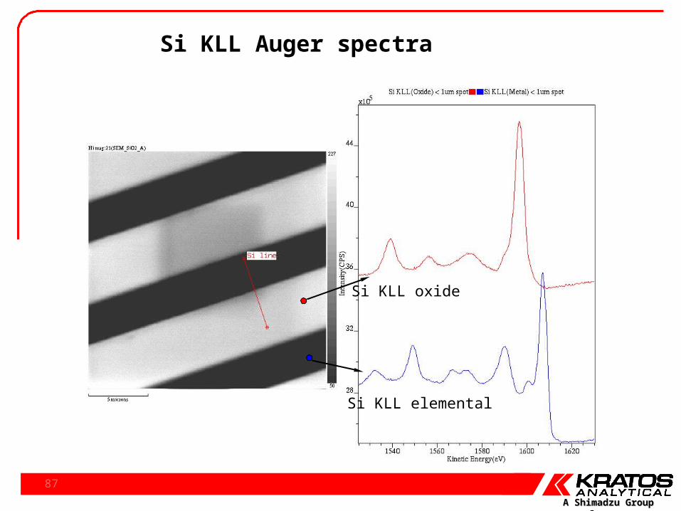
Si KLL Auger spectra
Si KLL oxide
Si KLL elemental
A Shimadzu Group CompanyA Shimadzu Group Company
88
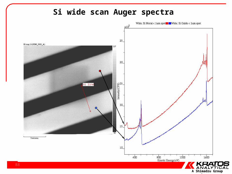
Si wide scan Auger spectra

A Shimadzu Group CompanyA Shimadzu Group Company
89
O KLL Auger map and SEM
20 microns 20 microns

A Shimadzu Group CompanyA Shimadzu Group Company
90
Atmospheric corrosion of nickel SEM images
I.Odnevall & C. Leygraf J.Electrochem. Soc., vol 144, No. 10, October 1997, 3518-3525
The atmospheric corrosion of nickel in a rural atmosphere – the formation of sulfate-containingcorrosion products with a characteristic dendritic morphology.

A Shimadzu Group CompanyA Shimadzu Group Company
91
Atmospheric corrosion of nickel AES after light etch
X
X
S
C
O
NiNi Ni
NiNi
Ni
CO
AES spectra show the presence of sulfur in the dendritic structure only.
dendrite
substrate

A Shimadzu Group CompanyA Shimadzu Group Company
92
Atmospheric corrosion of nickel AES maps
S (p-b) map O (p-b) map Ni (p-b) map
The images shown are peak - background maps.

A Shimadzu Group CompanyA Shimadzu Group Company
93
Duplex stainless steel UNS S32750 SEM & AES
X
X
Fe
NiNi
FeFe
CrCr
C
Fe
NiNi
FeCrCr
C
Fe
The sample was etched to remove the surface oxide before the SEMand AES were acquired. There was a slight difference in the Cr intensitybetween the two areas. Cr and Ni maps were acquired to investigateany spatial differences in their concentrations.
M. Femenia, J. Panl & C. Leygraf J.Electrochem. Soc., 151, (10) B581-B585 (2004)
In duplex stainless steels the alloying elements are not uniformly distributedbetween the two phases (austenite and ferrite). For example Cr and Mo partitionto the ferrite phase and Ni and N to the austenite.
aust
enite
ferr
ite
ferr
iteaustenite - light
ferrite - dark

A Shimadzu Group CompanyA Shimadzu Group Company
94
Duplex stainless steel UNS S32750 AES maps
Cr p-b map Ni p-b map
The Cr concentration is highest in the ferrite where the Ni concentration is lowest (austenite). The N concentration should be highest in the austenite region. Further AES spectra, with longer acquisition times, were recorded to try and detect the low level of nitrogen present.

A Shimadzu Group CompanyA Shimadzu Group Company
95
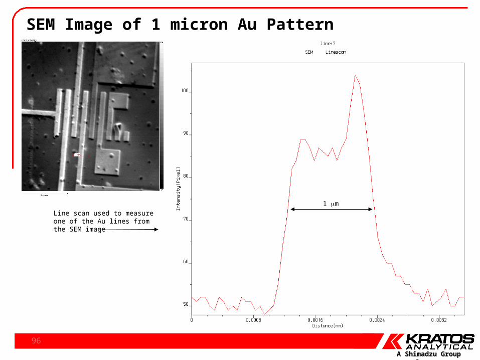
SEM Image of 1 micron Au Pattern on integrated IC
An SEM image of the Au pattern was recorded using a 30 micron field of view.
A Shimadzu Group CompanyA Shimadzu Group Company
96
SEM Image of 1 micron Au Pattern
1 m
Line scan used to measure one of the Au lines from the SEM image

A Shimadzu Group CompanyA Shimadzu Group Company
97
Au MNN
Al KLL
O KLL
C KLL
Au OPP
S LMM
Al LMM
Auger Spectroscopy
Auger spectra were recorded from on one of the pads (red) and the substrate (blue)

A Shimadzu Group CompanyA Shimadzu Group Company
98
Back Scattered Image of 1 micron Au Pattern
Sample was then etched and a back scattered image recorded with a 10 micron field of view.

A Shimadzu Group CompanyA Shimadzu Group Company
99
Auger Maps
Auger maps were recorded of the Au MNN and Al KLL peaks. Images displayed below are peak minus background maps recorded using 64 x 64 pixels and 100 ms dwell time. Total time for each image was 410 seconds (820 seconds for peak and background).
Au MNN Map Al KLL Map

A Shimadzu Group CompanyA Shimadzu Group Company
100
Auger Maps
Overlay of Au MNN and Al KLL peak minus background maps recorded using 150 x 150 pixels and 50 ms dwell time.

A Shimadzu Group CompanyA Shimadzu Group Company
101
Auger Maps: 100nm spatial resolution100 nm 80/20 resolution measured across a feature in Auger mapping mode.
A Shimadzu Group CompanyA Shimadzu Group Company
102
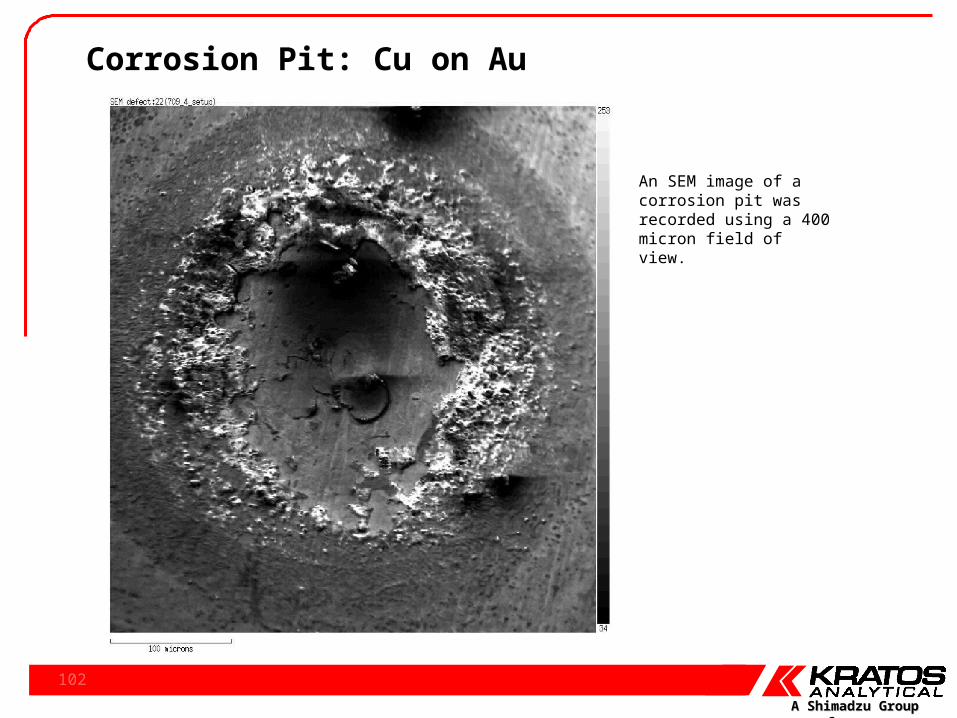
Corrosion Pit: Cu on Au
An SEM image of a corrosion pit was recorded using a 400 micron field of view.
A Shimadzu Group CompanyA Shimadzu Group Company
103
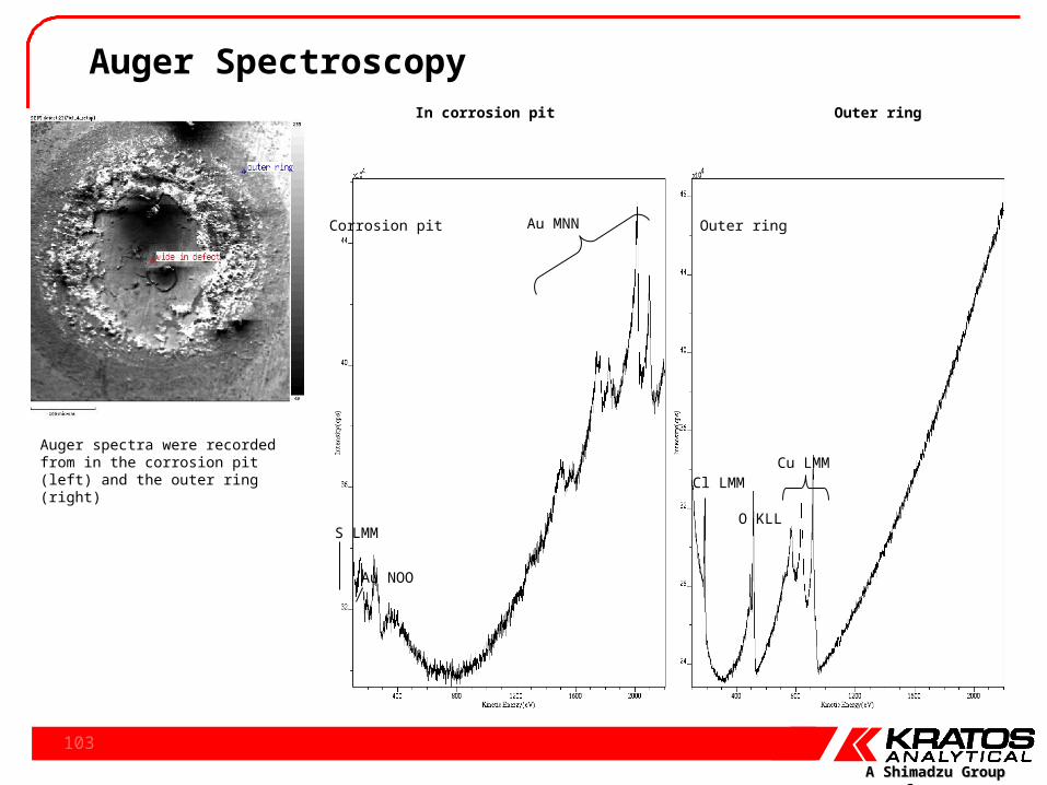
Auger Spectroscopy
Auger spectra were recorded from in the corrosion pit (left) and the outer ring (right)
In corrosion pit Outer ring
Au MNN
Au NOO
S LMM
Cu LMM
O KLL
Cl LMM
Corrosion pit Outer ring
A Shimadzu Group CompanyA Shimadzu Group Company
104
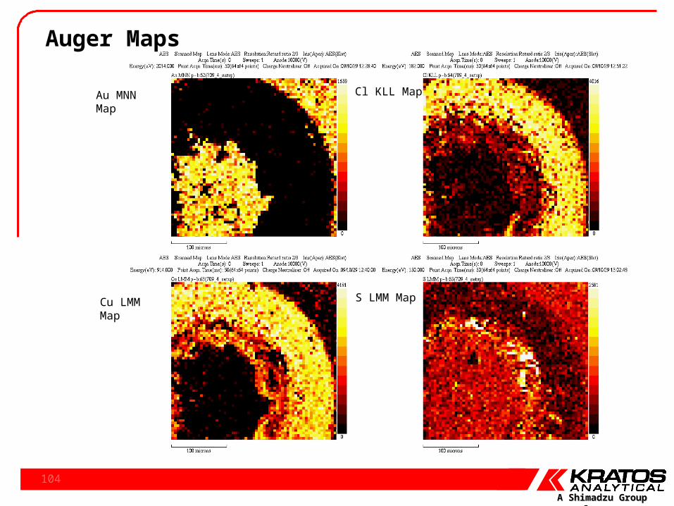
Auger Maps
Au MNN Map
Cl KLL Map
Cu LMM Map
S LMM Map

A Shimadzu Group CompanyA Shimadzu Group Company
105
Sample 4 : Auger Maps
Overlay of Au (red), Cu (green) and Cl (blue) peak minus background Auger maps

A Shimadzu Group CompanyA Shimadzu Group Company
106
SEM Image of Corrosion Pit following an etch
An SEM image of a corrosion pit was recorded following an Ar ion etch

A Shimadzu Group CompanyA Shimadzu Group Company
107
Auger Spectroscopy of corrosion product
Auger spectrum recorded from the corrosion product
Cu LMM
O KLLCl LMM

A Shimadzu Group CompanyA Shimadzu Group Company
108
Ultra Violet Photon Source
Optimized for maximum He (I) or He (II) (or Ne (l)/Ne (ll)) output.
1mm diameter guide to give a maximum lamp current of 37mA at17.5W
Minimum step size energy scale is 0.25meV in UPS mode.

A Shimadzu Group CompanyA Shimadzu Group Company
109
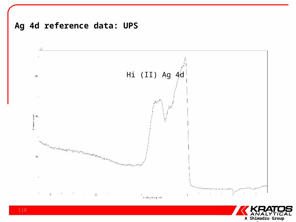
Ag EF = 95 meV.
Ag 4d reference data: UPS
>1.5MCPS
A Shimadzu Group CompanyA Shimadzu Group Company
110
Ag 4d reference data: UPS
Hi (II) Ag 4d

A Shimadzu Group CompanyA Shimadzu Group Company
111
XPS/UPS of synthetic diamond
Optical image of synthetic diamond
A Shimadzu Group CompanyA Shimadzu Group Company
112
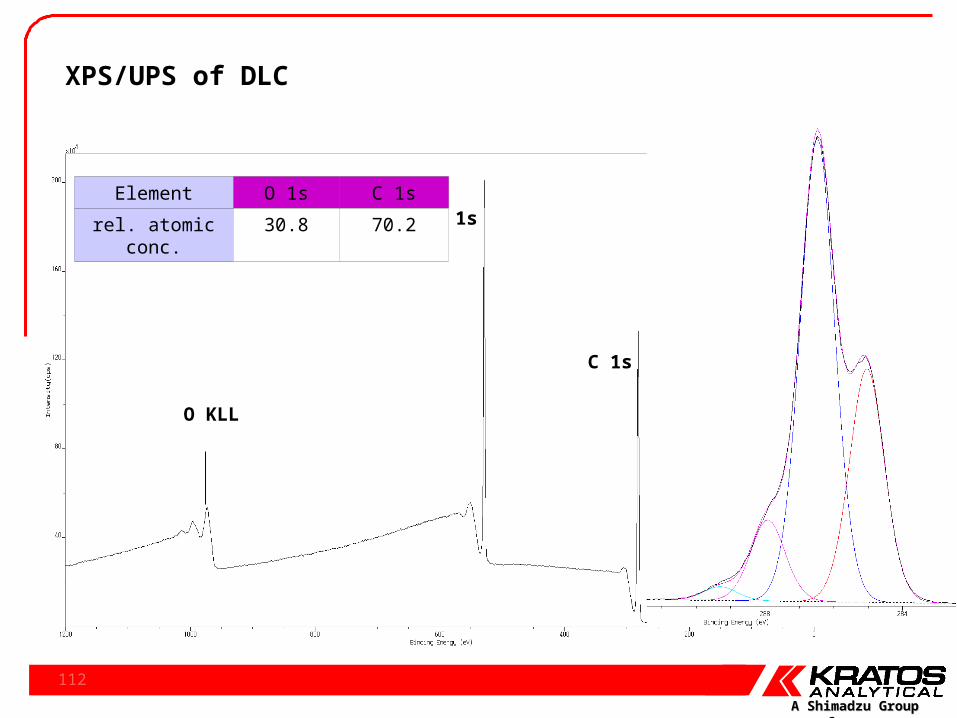
O 1s
C 1s
O KLL
XPS/UPS of DLC
Element O 1s C 1s
rel. atomic conc. 30.8 70.2

A Shimadzu Group CompanyA Shimadzu Group Company
113
Sample Heating
0
50
100
150
200
250
300
350
400
450
0.00 10.00 20.00 30.00 40.00 50.00 60.00
Heating time (minutes)
Tem
per
atu
re (
ºC)
Sample temperature (ºC)
Set temperature (ºC)
Sample heated to 450°C to reduce contamination
In-situ heating of DLC sample
Heating and cooling controlled directly from software
A Shimadzu Group CompanyA Shimadzu Group Company
114
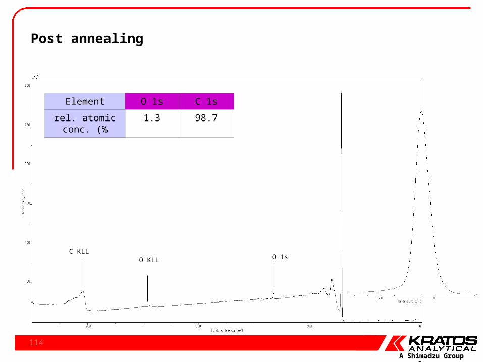
O 1sO KLL
Element O 1s C 1s
rel. atomic conc. (%
1.3 98.7
C KLL
Post annealing

A Shimadzu Group CompanyA Shimadzu Group Company
115
Heated Diamond Sample – He (I) UPS
EO= 17.8eV
EF = 0.73eV
Φ= 21.22eV – (17.8eV – 0.73eV)
Φ= 4.15eV

A Shimadzu Group CompanyA Shimadzu Group Company
116
Teflon tube
Silicon containing plasma
Small area XPS and XPS imaging

A Shimadzu Group CompanyA Shimadzu Group Company
117
Plasma treated polymer tube : survey spectrascanned spectra
plasma treatedend of tube
cut end of tube
Si 2
p
Si 2
s
C 1
s
N 1
s
O 1
s
F 1
s
F K
LL
O K
LL
survey spectra from 110um analysis area

A Shimadzu Group CompanyA Shimadzu Group Company
118
elemental concentration line scan
0
10
20
30
40
50
60
70
0 2000 4000 6000 8000 10000 12000
distance / um
conc
entr
atio
n (r
elat
ive
at. %
)
F 1s
O 1s
N 1s
C 1s
Si 2p
Concentration line scan by 110um, classic small area analysis
Several mm’s
Plasma

A Shimadzu Group CompanyA Shimadzu Group Company
119
Plasma treated polymer tube : high resolution spectrascanned spectra
N 1s region Si 2p1s region
plasma treatedend of tube
cut end of tube
plasma treatedend of tube
cut end of tube
C 1s region
plasma treatedend of tube
cut end of tube
plasma treatedend of tube
cut end of tube

A Shimadzu Group CompanyA Shimadzu Group Company
120
Carbon chemical state line scan
0
10
20
30
40
50
60
70
0 2000 4000 6000 8000 10000 12000
distance / um
rela
tive
co
nce
ntr
atio
n (
%)
C 1s CC,CH
C 1s C-O/CN
C 1s CF/C=O
C 1s CF2
C 1s CF3
CC
,CH
C-O
/C-N
C=
O/C
FC
F2
CF
3
CC
,CH
C-O
/C-N
C=
O/C
FC
F2
CF
3
CC
,CH
C-O
/C-N
C=
O/C
F
CF
2
CF
3
CC
,CH
C-O
/C-N
C=
O/C
F
CF
2
CF
3
plasma treated end
bulk polymer end
representative C 1s spectra as a function of position from the end of the tube
Plasma treated polymer tube : high resolution spectra

A Shimadzu Group CompanyA Shimadzu Group Company
121
Plasma treated polymer tube : Chemical state images
CC,CH (peak-background)parallel image at 285eV120 sec acquisition
CF2 (peak-background)parallel image at 292eV120 sec acquisition
overlay of CC,CH (red) with CF2 (green) parallel images
A Shimadzu Group CompanyA Shimadzu Group Company
122
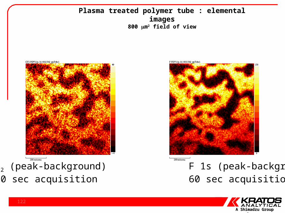
Plasma treated polymer tube : elemental images800 m2 field of view
CF2 (peak-background) F 1s (peak-background)120 sec acquisition 60 sec acquisition

A Shimadzu Group CompanyA Shimadzu Group Company
123
Plasma treated polymer tube : chemical state & elemental images400 m2 field of view
CC,CH (peak-background)parallel image at 285eV180 sec acquisition
CF2 (peak-background)parallel image at 292eV180 sec acquisition
F 1s (peak-background)parallel image at 689eV90 sec acquisition

A Shimadzu Group CompanyA Shimadzu Group Company
124
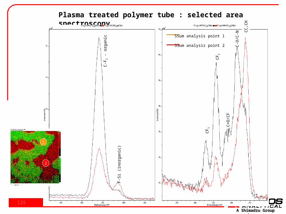
55um analysis areap1 (substrate)
55um analysis areap2 (plasma polymer)
F 1s
O 1s
N 1s
C 1s
Si 2pSi 2s
F 1s
O 1sN 1s
C 1s
Si 2pSi 2s
Plasma treated polymer tube : selected area spectroscopy400 m2 field of view
Analysis position Atomic Concn %
Fluorine Oxygen Nitrogen Carbon Silicon
Point 1 45.87 4.66 1.74 45.34 2.39
Point 2 27.33 9.87 6.11 50.07 6.72
A Shimadzu Group CompanyA Shimadzu Group Company
125
Plasma treated polymer tube : selected area spectroscopy400 m2 field of view
2
1
55um analysis point 1
55um analysis point 2
F-S
i (in
orga
nic)
C-F
2 -
org
anic
CC
,CH
C-O
/C-N
C=
O/C
F
CF
2
CF
3

A Shimadzu Group CompanyA Shimadzu Group Company
126
F 1s image 30 sec per image
Total acquisition time 5 mins
open, plasma treated end cut end of tube
Stitched images - 12 x 800 m2 field of view
Si concentration F concentration
A Shimadzu Group CompanyA Shimadzu Group Company
127
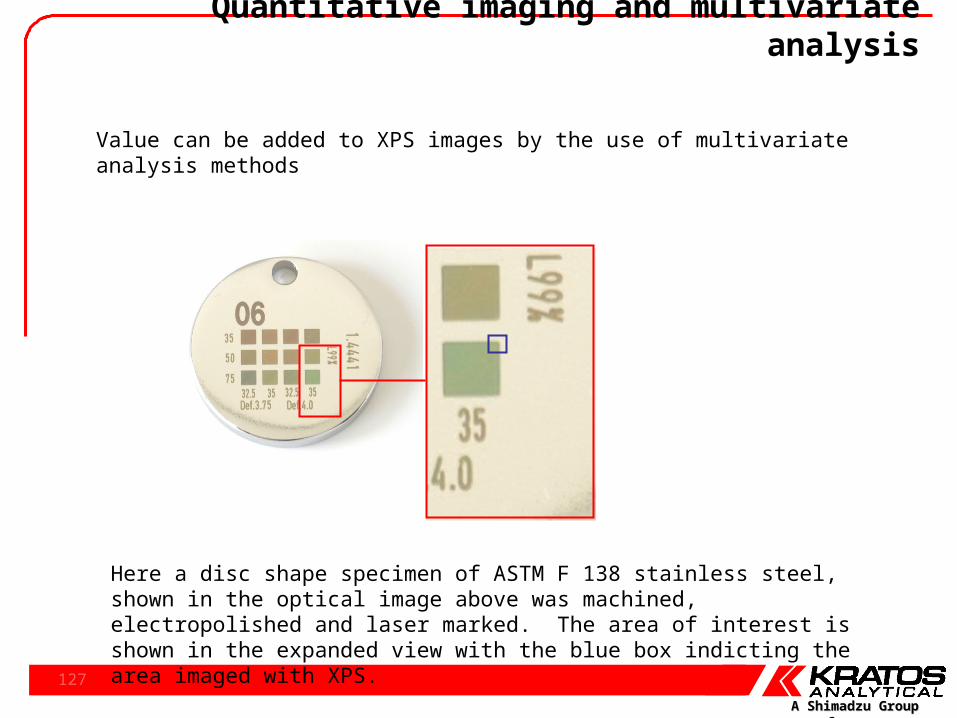
Value can be added to XPS images by the use of multivariate analysis methods
Here a disc shape specimen of ASTM F 138 stainless steel, shown in the optical image above was machined, electropolished and laser marked. The area of interest is shown in the expanded view with the blue box indicting the area imaged with XPS.
Quantitative imaging and multivariate analysis

A Shimadzu Group CompanyA Shimadzu Group Company
128
Printed using CasaXPS
Summed pixels (raw data)
x 10-2
14
16
18
20
22
24
26
28
30
32
CPS
720 718 716 714 712 710 708 706 704 702 700 698Binding Energy (eV)
Medical grade stainless steel Fe 2p images
Sum of pixels(raw data)
binding energy
Fe 2p images719eV 710eV (oxide) 706.5eV (metal) 700eV background
Fe 2p3/2
Acquire
Fe 2p3/2 multi-spectral images 720-698eV, 0.25eV steps, 30 s per image
Cr 2p multi-spectral images, 0.25eV steps, 30 s per image
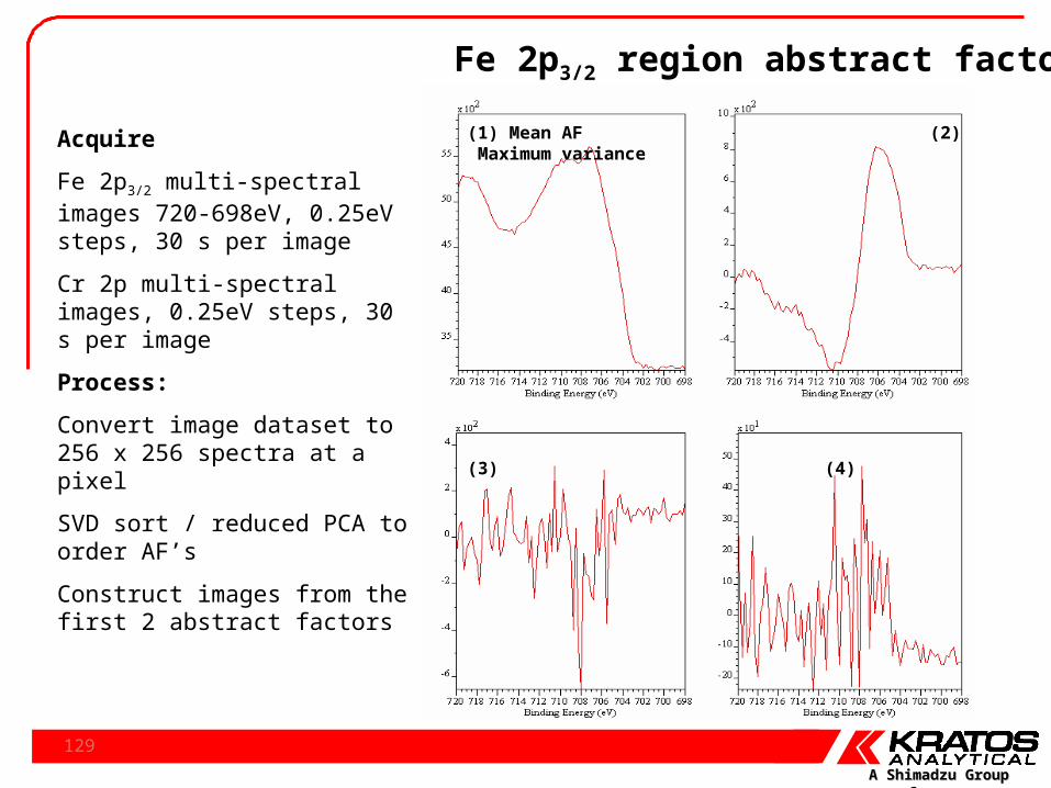
A Shimadzu Group CompanyA Shimadzu Group Company
129
Acquire
Fe 2p3/2 multi-spectral images 720-698eV, 0.25eV steps, 30 s per image
Cr 2p multi-spectral images, 0.25eV steps, 30 s per image
Process:
Convert image dataset to 256 x 256 spectra at a pixel
SVD sort / reduced PCA to order AF’s
Construct images from the first 2 abstract factors
(1) Mean AF (2) Maximum variance
(3) (4)
Fe 2p3/2 region abstract factors

A Shimadzu Group CompanyA Shimadzu Group Company
130
Raw & SVD/reduced PCA processed data
Printed using CasaXPS
Pr:Fe/1
x 10-2
14
16
18
20
22
24
26
28
30
32
CP
S
720 718 716 714 712 710 708 706 704 702 700 698Binding Energy (eV)
Raw data
SVD/reduced PCA processed
Summed pixel intensity from 256x256 pixels
Printed using CasaXPS
Fe/1
x 10-2
16
18
20
22
24
26
28
30
CP
S
720 718 716 714 712 710 708 706 704 702 700 698Binding Energy (eV)
Printed using CasaXPS
Fe/1
x 10-2
18
20
22
24
26
28
30
32
34
36
38
CP
S
720 718 716 714 712 710 708 706 704 702 700 698Binding Energy (eV)
Fit components to processed data corresponding to Fe oxide and Fe metal
Single pixel spectrum from metallic regionSingle pixel spectrum from oxide region

A Shimadzu Group CompanyA Shimadzu Group Company
131
Quantitative Cr and Fe images
• Cr image (red) shows enhanced concentration at the edge of the laser marked area
• Cr rich region at ‘corrosion front’• Fe metal (green) across entire sample but much lower concentration on laser
marked area• oxide layer thicker in laser marked area attenuates the Fe metallic
signal
Chromium relative atomic concentration image
Iron (metal) relative atomic concentration image

A Shimadzu Group CompanyA Shimadzu Group Company
132
Fe 2p 3/2
METALFe 2p 3/2
OXIDE
False colour range used to assign pixels
Raw pixels then summed to give “true” spectra from oxide and metal region
Pixel grouping

A Shimadzu Group CompanyA Shimadzu Group Company
133
Image stitching – high spatial resolution over large image areas
glass slide
poly(hydroxyethyl methacrylate)(pHEMA)
Acrylate, diacrylate, dimethylacrylate and triacrylate
combinations (as above)
D.G. Anderson, S. Levenberg & R. Langer Nature Biotechnology 22 (7) 863-866
Monomers used to generate sample array
1:40pm BO+PS+AS+SS TuA1 Room 201
“High throughput surface chemical analysis of polymer microarrays: Wettability, protein adsorption and cell response”

A Shimadzu Group CompanyA Shimadzu Group Company
134
Quantitative elemental stitched images
2mm 2mm 2mm
Fluorine (peak-background) Oxygen (peak-background) Carbon (peak-background)
● Quantitative elemental images corrected for transmission function and RSF● Thermal scale now indicates relative atomic concentration at a pixel
- each pixel represents 6.25um on the surface

A Shimadzu Group CompanyA Shimadzu Group Company
135
Quantitative elemental stitched images
Fluorine11.4 at%
0 at%
90.6 at% 60.8 at%Carbon
Oxygen32.5 at%
7.1 at%
2mm

A Shimadzu Group CompanyA Shimadzu Group Company
136
10 reasons why Axis Ultra is best selling XPS
• Only instrument to offer 0.48eV @ 400,000CPS• Excellent performance on insulators < 0.68eV PET• Largest analyser 165mm radius• DLD – pulse counting quantitative parallel imaging• DLD – snapshot mode 128 data channels• Fully automated control of all spot sizes• Electron only charge neutralisation system• Smallest analysis area 15um• Two analysers optimised for imaging and spectroscopy• Electrostatic deflection system for small area spectroscopy