A Scalable Time-based Integrate-and-Fire Neuromorphic...
23
A Scalable Time-based Integrate-and-Fire Neuromorphic Core with Brain-Inspired Leak and Local Lateral Inhibition Capabilities Muqing Liu, Luke R. Everson, Chris H. Kim Dept. of ECE, University of Minnesota, Minneapolis, MN [email protected] 1
Transcript of A Scalable Time-based Integrate-and-Fire Neuromorphic...

A Scalable Time-based Integrate-and-Fire Neuromorphic Core with Brain-Inspired Leak
and Local Lateral Inhibition Capabilities
Muqing Liu, Luke R. Everson, Chris H. Kim
Dept. of ECE, University of Minnesota, Minneapolis, MN
1
Outline
• Background
• Time Based Neural Networks
• Leaky Neuron and Local Lateral Inhibition
• Digit Recognition Application
• Measurement Results
• Conclusion
2

Neuromorphic Computing
• Biological neuron behavior: Weight multiplication (synapse) → Weight integration (cell body) → Threshold comparison & fire.
• Applications: Image recognition/classification, natural language processing, speech recognition, etc.
3
Biological neuron model
* synaptic weights: excitatory (+) or inhibitory (-)
Artificial neuron model
http://juanribon.com/design/nerve-cell-body-diagram.php

Prior Arts: Deep Learning Processor
• Circuit/Architecture innovations:
− Data reuse in convolutional neural network.
− Utilize sparsity by data gating/zero skipping.
− Reduced weight precision ���� binary neural networks.
4
(108KB)
Peak Performance:
16.8 – 42.0 GOPS
(1OP = 1MAC)
Power:
278mW @ 1V
4000µm4000µ
m
21mW @ 1.1V
3.9 TOPS/W @1.1V
235mW @ 1.1VEyeriss: DCNN Accelerator
DNPU: Reconfigurable CNN-
RNN Processor
TSMC 65nm LP 1P9M 65nm 1P8M CMOS
[1] Y.-H. Chen, et al., ISSCC, 2016. [2] D. Shin, et al., ISSCC, 2017.
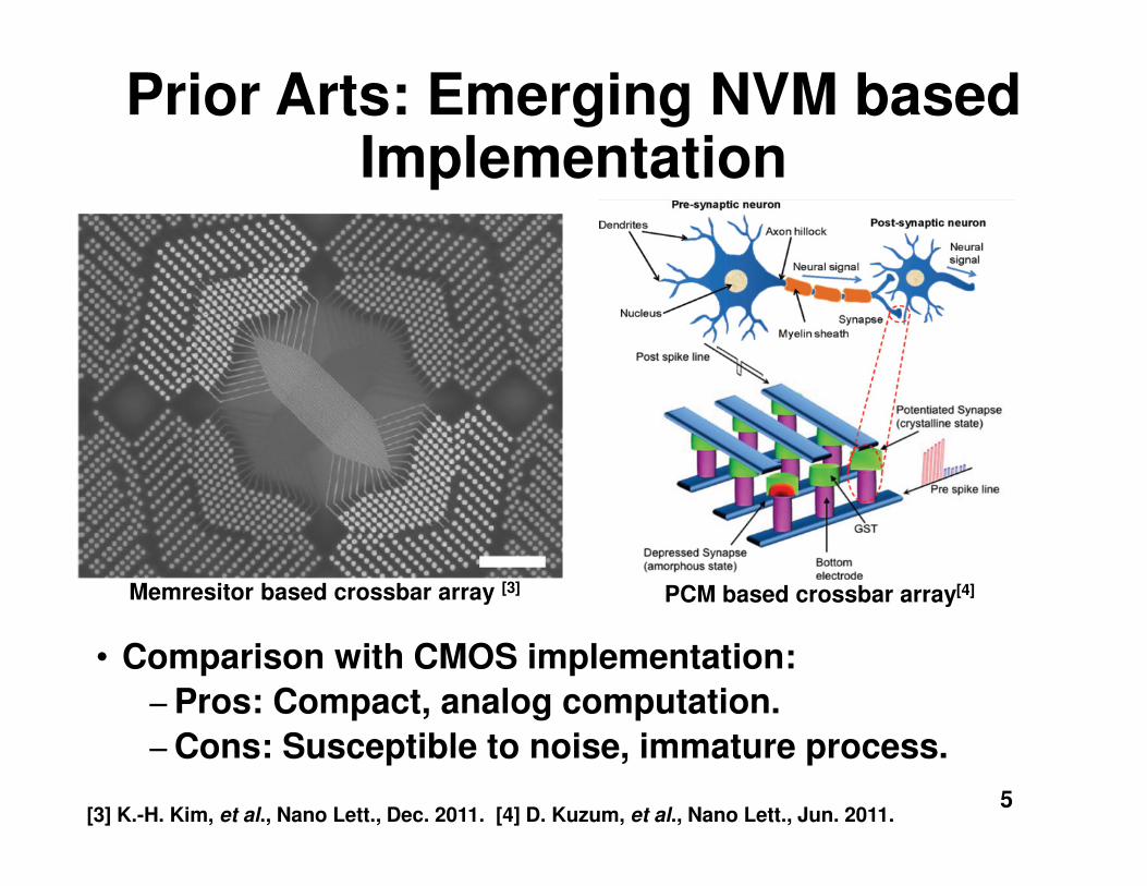
Prior Arts: Emerging NVM based Implementation
• Comparison with CMOS implementation:
− Pros: Compact, analog computation.
− Cons: Susceptible to noise, immature process.
5
Memresitor based crossbar array [3] PCM based crossbar array[4]
[3] K.-H. Kim, et al., Nano Lett., Dec. 2011. [4] D. Kuzum, et al., Nano Lett., Jun. 2011.

Time-based vs. Digital Implementation
6
x1·w1 +x2·w2 + ··· + xi·wi
x1·w1 x2·w2 xi·wi
Time
Delay1 Delay2 Delayi
Accumulate
∑∑∑∑
= Delay1 + Delay2 + ··· + Delayi
y = i xi·wi ∑∑∑∑y = i xi·wi
= x1·w1 +x2·w2 + ··· + xi·wi
N-bit Multipliers
x1
w1
∑
M-bit Adder
Activationx2
w2
xi
wi
Time-based Neural Network Digital Neural Network
Time-based Digital
Core circuits
Pros
Cons
Programmable delay circuits
Multipliers & adders
Area and power efficient High resolution
Moderate resolutionLarge area and power
consumption

Comparison with Previous Time-based Neural Network
7

Proposed Time-based Neural Net
8
SRAMSRAM
DCO with 128 Programmable Delay Stages
X0,X1
8b CounterDQ
QB
DQ
QB
DQ
QB
DQ
QB
Compare & Fire
C0C1C6C7
LLI
LEAKNeuron control logic
SPIKE
rstrstrstrst
Threshold8
Leaky Integrate & Fire, Local Lateral Inhibition
SRAM
SRAMSRAMSRAM
SRAMSRAMSRAM
SRAMSRAMSRAM
EN_DCO
SRAMSRAMSRA
MSRAMSRAMSRA
MSRAMSRAMSRA
MSRAMSRAMSRA
M
W0,1<2:0>
∑∑∑∑ ⋅⋅⋅⋅
====
wiXi
TDCOX2,X3
W2,3<2:0>X124,X125
W124,125<2:0>X126,X127
W126,127<2:0>
∑∑∑∑Delayi
∝ ∝ ∝ ∝
SPIKE

Proposed Time-based Neural Net
• Input pixel: Xi
− Determines whether a stage is activated or not.
• Weight: Wi<2:0>
− Determines how many capacitors are turned on asload in that stage.
9
SRAMSRAM
Programmable Delay Stage
Xi
SRA
M
Wi<2:0>
4C
SRA
M
WL
Xi
wi<2> wi<1> wi<0>
2C C
3 SRAM cells
5.9
µm
8.1µm
3 SRAM cells
SRA
M
SRA
M
Xi Xi
Unit cell layout (2 stages)
*BL,BLB omitted
for simplicity

64x128 Time-based Neural Network
• 8 DCO cores are groupedtogether to implement locallateral inhibition.
• 64 DCO neuromorphiccores in total.
• 121 out of 128 DCO stagesare used as programmableinputs.
• Remaining 7 stages are
reserved for calibration.
10

Frequency Calibration and Linearity Test
• Frequency variation between 10 DCOs
− Before calibration: 1.17%, after calibration: 0.10%.
11
Fre
qu
en
cy
(a
.u.)
000
001
010
011
100
101
110
111
Fre
qu
en
cy
(a.u
.)

• Leaky neuron: Ions diffuse through the neuron cell .
• Local lateral inhibition: Active neuron strives tosuppress the activities of its neighbors.
12
Lateral inhibition: Mach band illusion[4]Electrical modeling of cell membrane[3]
[3] W. Gerstner, et al., Neuronal Dynamics. [4] Wikipedia.
Bio-Inspired Features: Leaky Neuron and Local Lateral Inhibition (LLI)

Time-based Leak and LLI
13
DQ
QB
DQ
QB
rst
DQ
QB
rst
DQ
QB
rst
Compare & FireSPIKE
Time-based Leaky Integrate & Fire Neuron
Time-based Local Lateral Inhibition (LLI)
C
Threshold
LEAK
LLI
SPIKE<0> SPIKE<1> SPIKE<2> SPIKE<7>
LEAK
(LSB reset)
C0C1C6C7
rst
From
DCO
Neighbor
counter
bit reset
Ʃ+
-Ʃ
+
-Ʃ
+
-Ʃ
+
-Ʃ
+
-
• Leak enabled:− LSB of every counter
is reset periodically.
• LLI enabled:− Specific bits in the
neighboring countersare reset after a DCOspikes.
− The fastest DCO resetsthe other DCOs moreoften than it is reset byothers.

Leak and LLI
• Leak: Uniformly lower spiking frequency.
• LLI: Preferentially lower spiking frequency.
• Goal: Higher contrast between different neuron outputs.
14
*None: No leak and no LLI, basic DCO operation.
DCO No.0
Sp
ike
Fre
qu
en
cy
DCO No.0S
pik
e F
req
ue
nc
y*None LEAK
Sharper contrast
*None LLI
Sharper contrast

Handwritten Digit Recognition
15
• Input database: MNIST.
• Learning method: Supervised learning.
• Learning network: Single-layer & multi-layer perceptronnetwork.

Single-layer Digit Recognition
16
• Single-layer architecture: Proof-of-concept for time-based neural network

Multi-layer Digit Recognition
17
• Multi-layer architecture: Demonstrates the scalability ofthe core.

Measurement Results
18
*None: No leak and no LLI, basic DCO operation.
65nm LP CMOS, 1.2V, 25oC
82
84
86
88
90
92
94
Single-layer with 11x11
images
Two-layer with 11x11
images
Two-layer with 4-patch
22x22 images
Rec
og
nit
ion
Acc
ura
cy (
%)
Measured (*None)
Simulation
Measured (Leaky)
• Measured recognition accuracy from hardware iscomparable to software simulation results.

Measurement Results
19
9100
300
500
700
900
1100
1300
1500
0 1 2 3 4 5 6 7 8
Sp
ike C
ou
nt
1700
*None LLI1.7%
17.7%
(Target) Digit
65nm LP CMOS, 1.2V, 25oC
• Spike count difference between digit “2” and “0”
− Without LLI: 1.7%, with LLI: 17.7 %.
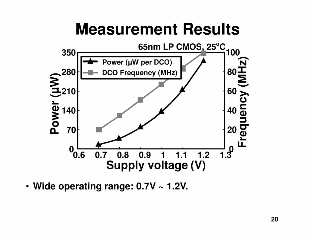
Measurement Results
20
0
70
140
210
280
350P
ow
er
(µW
)
0.6 0.7 0.8 0.9 1 1.1 1.2 1.3
Supply voltage (V)
0
20
40
60
80
100
Fre
qu
en
cy (
MH
z)
DCO Frequency (MHz)
Power (µW per DCO)
65nm LP CMOS, 25oC
• Wide operating range: 0.7V ~ 1.2V.

Performance Comparison
21
[5] D. Miyashita, et al., ASSCC, 2017. [6] K. J. Lee, et al., ISSCC, 2016. [7] J. K. Kim, et al., VLSI, 2015.
This work
ApplicationHand writing recognition
Technology 65nm
Area 0.24mm2 (64 DCOs)
Voltage 1.2V
Frequency 99MHz (nominal DCO freq.)
FunctionMulti-layer perceptron
network
Performance Comparison
16.6GE/PEc
Power
ISSCC’16 [6]
Object detection + intention prediction
65nm
16.0mm2
1.2V
250MHz
Deep neural network
330mW
Power Efficiency
309G ÷ N spikes/s/W(N=spiking thresholda)
-
320.4 µW/DCO
Circuit Type Time-based Analog + Digital
VLSI’15 [7]
Object Recognition
65nm
1.8mm2
0.45V
Spiking LCA with classification
5.7pJ/pixel (memory+logic)
3.65mW
-
Digital
40MHz (Inference)
ASSCC’17 [5]
Hand writing recognition
65nm
3.61mm2 (32K PEs)
-
Convolutional neural network
48.2TSOp/s/W
-
Time-based
-
862GOPS/W
862GOPS/W
-
-5.7pJ/pixel
(memory+logic)
-
-
37.4TOPS/Wd
0.43pJ/pixel (logic)e
Note
a. N=16 in our measurements.
b. SOp/s/W: Synaptic operation (SOp). In DCO based time-domain neural network, one oscillation of DCO is equivalent to 121 SOp.
c. 1GE: 1.44um2(65nm). PE: processing element.
d. Operation: One operation is defined as one multiplication and accumulation (MAC). In DCO based time-domain neural network, one oscillation of DCO is equivalent to 121 3-bit MAC.
e. Used spiking threshold of 16, and only accounted for the power consumption of core logic circuits, memory power is not included, since weight is not updated during the inference.
Hardware Efficiency
- 76.5GE/PE - -
76.5GE/PE
48.2TSOp/s/W37.4TSOp/s/Wb
- -

Die Photo and Performance Summary
22
Conclusion
• Neural network function is computed in timedomain using standard digital circuits with higharea and power efficiency.
• Implemented brain-inspired leak and locallateral inhibition features to enhance thecontrast between neuron outputs.
• 65nm test chip measurements confirm 91%hand-written digit recognition accuracy.
23