A Robust 96.6-dB-SNDR 50-kHz-Bandwidth Switched-Capacitor … · 2017-07-25 · sensors Article A...
19
sensors Article A Robust 96.6-dB-SNDR 50-kHz-Bandwidth Switched-Capacitor Delta-Sigma Modulator for IR Imagers in Space Instrumentation † Michele Dei 1, *, Stepan Sutula 1 , Jose Cisneros 1 , Ernesto Pun 2 , Richard Jan Engel Jansen 3 , Lluís Terés 1,4 and Francisco Serra-Graells 1,4 1 Instituto de Microelectrónica de Barcelona IMB-CNM(CSIC), 08193 Barcelona, Spain; [email protected] (S.S.); [email protected] (J.C.); [email protected] (L.T.); [email protected] (F.S.-G.) 2 Arquimea Ingenierìa S.L.U., 28918 Madrid, Spain; [email protected] 3 European Space Research and Technology Centre, 2201 AG Noordwijk, The Netherlands; [email protected] 4 Department of Microelectronics and Electronic Systems of Universitat Autònoma de Barcelona, 08193 Barcelona, Spain * Correspondence: [email protected]; Tel.: +34-935-94-77-00 (ext. 2492) † This paper is an extended version of our paper published in Proceedings of the IEEE International Symposium on Circuits and Systems, Montréal, QC, Canada, 22–25 May 2016; pp. 61–64. Academic Editor: A. G. Unil Perera Received: 13 April 2017; Accepted: 31 May 2017; Published: 2 June 2017 Abstract: Infrared imaging technology, used both to study deep-space bodies’ radiation and environmental changes on Earth, experienced constant improvements in the last few years, pushing data converter designers to face new challenges in terms of speed, power consumption and robustness against extremely harsh operating conditions. This paper presents a 96.6-dB-SNDR (Signal-to-Noise-plus-Distortion Ratio) 50-kHz-bandwidth fourth-order single-bit switched-capacitor delta-sigma modulator for ADC operating at 1.8 V and consuming 7.9 mW fit for space instrumentation. The circuit features novel Class-AB single-stage switched variable-mirror amplifiers (SVMAs) enabling low-power operation, as well as low sensitivity to both process and temperature deviations for the whole modulator. The physical implementation resulted in a 1.8-mm 2 chip integrated in a standard 0.18-μm 1-poly-6-metal (1P6M) CMOS technology, and it reaches a 164.6-dB Schreier figure of merit from experimental SNDR measurements without making use of any clock bootstrapping, analog calibration, nor digital compensation technique. When coupled to a 2048 × 2048 IR imager, the current design allows more than 50 frames per minute with a resolution of 16 effective number of bits (ENOB) while consuming less than 300 mW. Keywords: infrared imager (IR); analog-to-digital converter (ADC); delta-sigma modulator (DSM); switched capacitors (SC); class-AB operational amplifiers 1. Introduction High levels of miniaturization are required in space for the realization of sensitive optical and radiation detector arrays. These detector arrays are used to map the particles, as well as the photons originating from stars and planets over the whole energy spectrum with the purpose to monitor the state of vegetation and pollution on Earth, as well as investigating the physical state and functioning of our surrounding universe. From the different detector arrays for the observation of particles, X-rays, UV, visible, infrared and far infrared radiation, the imaging of near and far infrared proves to be the most challenging. These detector arrays consist of multi-millions of pixels that have to readout at Sensors 2017, 17, 1273; doi:10.3390/s17061273 www.mdpi.com/journal/sensors
Transcript of A Robust 96.6-dB-SNDR 50-kHz-Bandwidth Switched-Capacitor … · 2017-07-25 · sensors Article A...

sensors
Article
A Robust 96.6-dB-SNDR 50-kHz-BandwidthSwitched-Capacitor Delta-Sigma Modulator for IRImagers in Space Instrumentation †
Michele Dei 1,*, Stepan Sutula 1, Jose Cisneros 1, Ernesto Pun 2, Richard Jan Engel Jansen 3,Lluís Terés 1,4 and Francisco Serra-Graells 1,4
1 Instituto de Microelectrónica de Barcelona IMB-CNM(CSIC), 08193 Barcelona, Spain;[email protected] (S.S.); [email protected] (J.C.);[email protected] (L.T.); [email protected] (F.S.-G.)
2 Arquimea Ingenierìa S.L.U., 28918 Madrid, Spain; [email protected] European Space Research and Technology Centre, 2201 AG Noordwijk, The Netherlands;
[email protected] Department of Microelectronics and Electronic Systems of Universitat Autònoma de Barcelona,
08193 Barcelona, Spain* Correspondence: [email protected]; Tel.: +34-935-94-77-00 (ext. 2492)† This paper is an extended version of our paper published in Proceedings of the IEEE International
Symposium on Circuits and Systems, Montréal, QC, Canada, 22–25 May 2016; pp. 61–64.
Academic Editor: A. G. Unil PereraReceived: 13 April 2017; Accepted: 31 May 2017; Published: 2 June 2017
Abstract: Infrared imaging technology, used both to study deep-space bodies’ radiation andenvironmental changes on Earth, experienced constant improvements in the last few years,pushing data converter designers to face new challenges in terms of speed, power consumptionand robustness against extremely harsh operating conditions. This paper presents a 96.6-dB-SNDR(Signal-to-Noise-plus-Distortion Ratio) 50-kHz-bandwidth fourth-order single-bit switched-capacitordelta-sigma modulator for ADC operating at 1.8 V and consuming 7.9 mW fit for spaceinstrumentation. The circuit features novel Class-AB single-stage switched variable-mirror amplifiers(SVMAs) enabling low-power operation, as well as low sensitivity to both process and temperaturedeviations for the whole modulator. The physical implementation resulted in a 1.8-mm2 chipintegrated in a standard 0.18-µm 1-poly-6-metal (1P6M) CMOS technology, and it reaches a 164.6-dBSchreier figure of merit from experimental SNDR measurements without making use of any clockbootstrapping, analog calibration, nor digital compensation technique. When coupled to a 2048× 2048IR imager, the current design allows more than 50 frames per minute with a resolution of 16 effectivenumber of bits (ENOB) while consuming less than 300 mW.
Keywords: infrared imager (IR); analog-to-digital converter (ADC); delta-sigma modulator (DSM);switched capacitors (SC); class-AB operational amplifiers
1. Introduction
High levels of miniaturization are required in space for the realization of sensitive opticaland radiation detector arrays. These detector arrays are used to map the particles, as well as thephotons originating from stars and planets over the whole energy spectrum with the purpose to monitorthe state of vegetation and pollution on Earth, as well as investigating the physical state and functioningof our surrounding universe. From the different detector arrays for the observation of particles, X-rays,UV, visible, infrared and far infrared radiation, the imaging of near and far infrared proves to bethe most challenging. These detector arrays consist of multi-millions of pixels that have to readout at
Sensors 2017, 17, 1273; doi:10.3390/s17061273 www.mdpi.com/journal/sensors

Sensors 2017, 17, 1273 2 of 19
increasingly higher speeds and higher accuracy at minimal power expenditure, such as to minimizethe induced thermal noise. At the turn of the century, the state-of-the-art detector array technologyand readout electronics [1,2] consisted of 2048× 2048 detector arrays manufactured either with CCDand CMOS technology with HgCdTe detector material for the infrared radiation (IR). Commonconfigurations of pixel readout circuitry comprise source follower (SF), capacitive transimpedanceamplifier (CTIA) and direct injection (DI) depending on the flux quantity over the exposure periodof time and the specific wavelength range of the application. The detector array control and signalconversion component in [3] could readout up to 36 channels in parallel. Per channel signal conversioncould be realized at 100 kS/s to 14 bit accuracy per ADC for 1.3 mW power. The control and signalconversion component set the detector supply, bias voltages and supplied the detector readout clockingscheme, as well as configuration via a serial bus. This detector array with the attached readoutcomponent together with the control and signal conversion component proved to be successful andhas been used in many payload missions as employed for astronomical observation on Earth.
Over the ensuing years, the scientific requirements for increasing precision and resolution ledto larger detector arrays [4], higher accuracy through the suppression of the detector dark currents [5,6]and increasing dynamic range [7]. With improved readout electronic components [8], linearity couldbe increased and noise minimized to cover and exceed the current generation of control and signalconversion components [9,10] under development. Detector array sizes increased from 2048× 2048to 4096× 4096. At the same time, the dynamic range as expressed as the ratio of the maximum electroncharge to noise has increased from 14 bits to 16 bits. The increased detector size has led to an increase inreadout channels that have to be processed in parallel with a minimum increase in power consumptionsuch as to minimize the thermal noise. The increased detector signal dynamic range beyond 90 dB hasto be addressed with an improved ADC, which is described in the following sections.
Typically, the component should consume less than 600 mW of power such as to allow efficientheat extraction in space. In addition to being radiation tolerant and having highly reliability, it shouldoperate under an extended temperature range, including cryogenic temperatures down to 35 K.At least 36 ADC and with each of them an offset correction DAC should be provided to shift thedetector output voltage range. After offset correction, programmable gain should ensure that the fulldetector output signal range can be converted with the ADC. A sampler prior to the ADC shouldenable correlated double sampling, as well as speeding-up the readout by combining the channels viaa multiplexer. The channels require also a programmable current source DAC to bias their open drainreadout transistor. Moreover, each of the channels should have its own dedicated reference voltagewith overcurrent and short circuit protection. The detector supply should also be provided. Thehouse keeping ADCs should be supported with the current source to allow temperature readout fromtemperature sensors, as well as monitoring currents and reference voltages. In Figure 1a, a functionaldiagram of the detector and readout control and signal conversion component is depicted. As thedetector with the readout circuit can be tiled to cover a larger surface area, the control and conversioncomponent should not be larger in size than the detector itself.
The control and signal conversion component should provide the detector and its readout circuitwith supply, bias voltages, configuration data, detector pixel reset and readout clocking signals, as wellas provide the signal conditioning and conversion. In addition to these detector and readout supports,control and processing functions, it should monitor supply current, temperature and reference voltageand should transmit the collected data to the connected data processing unit through a high speeddigital interface (HSDI). These operations are controlled by an on-chip sequencer that can be configuredby the connected data processing unit.
The functional and operation requirements on this image detector control and signal conversioncomponent put demanding constraints on the ADC in terms of accuracy, bandwidth, powerconsumption and area.
This paper presents a low-power SC ΔΣM for ADC with a 96.6-dB peak Signal-to-Noise-plus-Distortion Ratio (SNDR) and a 50-kHz bandwidth, operating at the nominal 1.8-V supply voltage of the

Sensors 2017, 17, 1273 3 of 19
CMOS process, and it does not require any analog calibration, DEM or digital compensation technique.This performance is mainly achieved by the introduction of Class-AB single-stage variable-mirroramplifiers (VMAs), first proposed by these authors in [11], combined with a power-aware modulatordiscrete-time (DT) architecture and a five-phase SC scheme. This work was introduced in [12], butextensive new material is included here concerning ΔΣM architecture selection and performance,circuit-block specifications, switched-VMA operation, ΔΣM robustness against technology mismatch,process and temperature variations and expanded state-of-the-art comparison.
Figure 1. Application-specific integrated circuit (ASIC) concept for IR imagers in space instrumentation.
The presented paper is organized as follows: Section 2 reviews the state-of-the-art ΔΣ-ADCswith emphasis on the current application. Section 3 describes the selection of the ΔΣM architecturebased on power and robustness considerations. Then, the ΔΣM SC topology with switched-VMAsand a five-phase switching scheme is analyzed in Section 4, together with the amplifiers’ requiredperformance. Section 5 proposes the Class-AB single-stage switched VMA to be used in all amplifierblocks of the noise shaper, providing a detailed analysis of its circuit operation. Section 6 presentsthe ΔΣM robustness against process and temperature from transistor-level simulations. Finally,the experimental results in 0.18 µm-CMOS technology and a comparative analysis with state-of-the-arthigh-resolution ADCs are reported in Section 7.
2. ΔΣ ADC for Space Instrumentation
The integration of high-resolution data converters in CMOS technologies with increasing processvariability and supply-voltage downscaling has become a circuit design challenge. This fact canbe noticed by the small number of circuit implementations reported in the literature, like [13–23],compared to other regions of the ADC design universe with similar figure of merit values [24].
From the architectural viewpoint, both discrete-time (DT) and continuous-time (CT) delta-sigmamodulators (ΔΣMs) are the common choice for high-resolution data converters, as they tend to relaxthe specifications of analog blocks at the expense of increasing oversampling ratios. Continuous-time

Sensors 2017, 17, 1273 4 of 19
strategies based on active-Resistor-Capacitor (RC) [13,15,18,21,23] or transconductor-capacitor(Gm-C) [19] implementations are attractive due to their built-in anti-aliasing filtering and the low-speedrequirements for their active circuits. However, CT techniques can suffer from both clock-jitter andtechnology sensitivity, and special attention must be paid to excess loop delays in the feedback DAC.Moreover, CT noise shapers may require in practice accurate tuning circuits. On the other hand,discrete-time (DT) ΔΣM realizations relying on switched-capacitor (SC) [14,16,17,20,22] or switched-RC(SRC) [25] circuits can exploit their advantages in terms of low sensitivity to clock jitter, the highlinearity of integrated capacitors and matching-based design methodologies. All of these points usuallycompensate for the increase of circuit area, which, in turn, can be mitigated if CMOS technologies withstacked metal-insulator-metal (MIM) or fringing capacitors are available.
Recent advances in CT shapers proved excellent power efficiency, despite the aforementionedshortcomings. On the other hand, robustness and DT shapers are essential for the required application.Hence, a deeper analysis of DT-SC shapers’ power consumption is needed. In this latter case, powerconsumption is identified by two contributions: static current is constantly drawn from the suppliesto bias the active blocks, plus an impulsive current is needed to charge the capacitors at the pace ofthe clock frequency. In SC ΔΣMs, this problem is aggravated due to the oversampling nature of themodulation. Moreover, even in the condition of constant zero input, the modulator internal statevariables are incessantly updated at each clock cycle due to the non-linear feedback of the system.This implies that the dynamic power consumption is practically independent of the input signal level.When operated in Class-A, the amplifiers’ bias currents must be at least on the same level as thepeak impulsive currents demanded for the given settling requirements, making the static currentcontribution dominant over the dynamic one. To avoid this issue, active blocks operating in Class-ABare a common choice [26]. Finally a further 50% reduction of static power consumption can be achievedemploying the switched-OpAmp technique [27], which consists of turning off the amplifiers duringtheir inactive clock phase.
3. ΔΣ Architecture Selection
Figure 2 presents the one-bit fourth-order feedforward single-loop ΔΣM architecture chosen for thehigh-resolution ADC, targeting a 16-bit dynamic range, a 50-kHz bandwidth and a 2.4-Vpp differentialinput full-scale. In this sense, the 16-bit specification is initially extended to SNDRmax = 110 dBin order to gain a two-bit safety margin for the rest of the ΔΣM circuit design methodology. AlthoughFigure 2 is a behavioral DT model only, several design decisions have already been made at this levelaffecting its CMOS circuit implementation, especially from the power-consumption viewpoint.
Coefficient Value
a1 0.2
a2 0.4
a3 0.1
a4 0.1
b1 1
b2 1
b3 1
b4 2
Figure 2. Differential-signal discrete-time (DT) model of the 1-bit 4th-order feedforward single-loopΔΣM architecture. The a1−4, b1−4 values are alike the ones used in [28].
The first and most noticeable design choice in the ΔΣM of Figure 2 is about the use of a single-looparchitecture instead of multi-stage noise-shaping (MASH) alternatives [29]. This decision is related

Sensors 2017, 17, 1273 5 of 19
to the difficulty of obtaining the high-resolution analog matching between MASH stages required tobenefit from the feedforward error-cancellation mechanism. In counterpart, and because of the highloop order demanded by the target dynamic range, special care must be taken to select a safe set ofgain coefficients to ensure modulator stability, as explained later in this section.
Secondly, multiple feedforward paths [30] are incorporated into the ΔΣM of Figure 2.This architectural strategy allows reducing the signal components following the first integratorand investing in the high-gain integrating stages to process quantization noise mainly. As a result,specifications for the integrators’ amplifiers can be relaxed due to the lower signal content in theinternal full scale. In practice, it can be shown that a reduction of circuit power consumption can beobtained when using feedforward paths for a given order of noise shaping [31].
Architectures based on multi-bit quantizers are attractive mainly because they allow one to reducethe slew rate requirements of OpAmps by lowering the amplitude of error signals inside the noiseshaper with a clear benefit in terms of power consumption. Multi-bit quantization can be achievedusing arrays of comparators, but circuit complexity increases exponentially with the number of bits.Power-efficient implementation of multi-bit quantization is currently a hot topic: solutions based onthe successive approximation register (SAR) quantizer [15,32] or tracking quantizers [33] are popularsince their power consumption scales linearly with the number of bits [32]. Alternatively, quantizersoperating time-to-digital conversion (TDC) received special attention as they also promise to bevery power efficient [34]. Nevertheless, to the authors knowledge, robust implementations againsttemperature process and voltage corners are hard to find. Finally, mismatch in the unit elementsof the feedback DAC affects negatively the SNDR, and correction techniques, either calibration [13]or dynamic element matching [35], need to be employed at the cost of increased circuit complexity.Clearly, in all of the reviewed multi-bit solutions, quantizer/DAC power is traded for amplifiers’power. In this design, we opted for the single-bit quantizer solution due to its robustness againsttechnology mismatch, its inherent linearity and design simplicity, while power optimization is enabledthanks to the new family of Class-AB amplifiers. It must be said that the use of these special amplifiersdoes not prevent multi-bit solutions to be employed.
At this point, there is a clear trade off between shaping order and oversampling ratio (OSR).Selecting a high-order shaping solution effectively lowers the OSR, so circuit speed requirements,but at the cost of increasing ΔΣM-loop instability issues. On the other hand, high OSR values requiremore power-efficient circuits, but they can reduce both the number of active blocks and also thearea of the input sampler. Based on the 110-dB SNDRmax target, a fourth-order shaping transferfunction is chosen in Figure 2 combined with a moderate OSR of 136, which results in a samplingrate of 13.6 MS/s for a 50-kHz bandwidth. The behavioral simulation of the final ΔΣM architecturegives the results of Figure 3 when including the thermal noise of the input sampler. In particular, themaximum tolerated noise floor to satisfy the SNDRmax specification at room temperature imposes aminimum single-ended input sampling capacitance (Cs1) exceeding 41 pF.
Although the chosen ΔΣM architecture differs from the latter by the absence of the z−1 delay inthe first and third stages due to the switched-OpAmp operation explained in the next section, the sameset of coefficients proves the good robustness against technology mismatching up to more than 5%,as noticed from the behavioral simulation results of Figure 4a.
Transient settling errors are studied for the DT integrators of Figure 2 to foresee possiblepower consumption bottlenecks before starting with the actual SC circuit design of the next section.A non-linear model is built for this purpose inspired by the combined response of the amplifier slewrate (SR) and gain-bandwidth product (GBW) [36]. The results obtained from the correspondingbehavioral simulation of Figure 4b reveal that a maximum settling error below 0.04% should beensured when designing each amplifier circuit.
The digital output stream dout in Figure 2 is finally processed by an attached FPGA, which isin charge of filtering the out-of-band modulation noise and decimating the sample rate down to the

Sensors 2017, 17, 1273 6 of 19
original Nyquist bandwidth of the signal. A dedicated decimator filter has not been implemented hereto allow for reconfigurability with respect to different IR sensor setups.
103 104 105 106
Frequency [Hz]
−160
−140
−120
−100
−80
−60
−40
−20
0
Pow
ersp
ectr
alde
nsit
y[d
BFS]
80 dB/dec
−125 −100 −75 −50 −25 0Input amplitude [dBIFS]
0
20
40
60
80
100
120
SND
R,S
NR
,SD
R[d
B]
SNDRSNRSDR
−10 −8 −6 −4 −2106112118124(a) (b)
Figure 3. Behavioral simulation results for the ΔΣM of Figure 2 considering quantization errorsand input-sampler thermal noise: output spectra for −3.35-dBIFS (IFS: internal full scale) 13.28-kHzeight-cycle input with SNDR = 110 dB (a) and dynamic range at the same frequency (b).
0.0 2.5 5.0 7.5 10.0Coefficient mismatch error [%]
−20
0
20
40
60
80
100
120
SND
R[d
B]
SimulationcasesFull scale,worst caseHalf full scale,worst case
0.001 0.01 0.1 1.0Integrator settling error [%]
100
102
104
106
108
110
112
114
116
SND
R[d
B]
(a) (b)
Figure 4. Simulated SNDR losses in the ΔΣM architecture of Figure 2 due to coefficient technologymismatch; worst case interpolation lines are given for input full scale (solid) and half full scale(dashed) (a); SNDR losses due to settling error at integrator outputs (b).
4. ΔΣ Modulator SC Topology
Figure 5 shows the SC network proposed for implementing the one-bit fourth-order feedforwardsingle-loop ΔΣM architecture of Figure 2. The sizing of the sampling capacitor for each stage detailed

Sensors 2017, 17, 1273 7 of 19
in Table 1 is derived from the Cs1 thermal-noise specification of the previous section and the followingnoise-shaping scaling rule [31]:
Csi = Cs1π2i−2
OSR2i−2 (2i− 1)
i
∏k=2
1a2
k−1for i > 1, (1)
where ak−1 stands for the gain of the (k− 1)-th integrator. The other capacitor sizes of Table 1 directlycome from the rest of the coefficients of Figure 2. It is worth noting at this point the large capacitancevalues obtained for the first stage (i.e., Cs1, Cfb and Ci1). This challenging specification, which allowsone to keep the signal full scale within the nominal CMOS supply voltage (1.8 V) and to avoid anybootstrapping at the input stage, demands very efficient Class-AB amplifiers for low-power operation,as proposed in the next section.
Figure 5. SC topology proposed for the ΔΣM architecture of Figure 2 with the switched-variable-mirroramplifier (SVMA) and five-phase switching scheme. The phase subindex indicates the special state(1 = closed, 0 = open) during ADC initialization (den = 0).
Table 1. Capacitor sizing in pF for the SC ΔΣM of Figure 5.
Capacitance Value Capacitance Value Capacitance Value
Cfb 21.16 Cff0 0.92
Cs1 42.32 Ci1 211.6 Cff1 0.92
Cs2 3.68 Ci2 9.2 Cff2 0.92
Cs3 0.92 Ci3 9.2 Cff3 0.92
Cs4 0.92 Ci4 9.2 Cff4 1.84
Switched-OpAmp operation is employed in all integrators of the ΔΣM. In our context, its mainpurpose is not only to replace the critical series switches at the output of each stage, which can introducedistortion issues due to their signal-dependent resistance, but also to save DC current consumptionthanks to the 50% duty cycle of each amplifier. In this sense, the clock phase controlling the on-offstate of each amplifier in Figure 5 is indicated inside its symbol following the same nomenclatureas for the rest of the switching elements. It is important to highlight that all switches are implementedusing simple complementary N/PMOS transmission gates and operated at the nominal supply voltageof the target CMOS technology without any clock-bootstrapping technique, which is incompatiblewith the high-reliability standards of space applications since it heavily overstress the gate oxideof the sampling devices, degrading the signal quality and finally shortening their lifetime [37].
As already discussed in the previous section, a passive capacitive divider is employed in Figure 5for the summation of all feedforward signals coming from the nested paths. This solution has a double

Sensors 2017, 17, 1273 8 of 19
benefit in terms of low-power operation, since it avoids the DC current consumption of OpAmp-basedactive summers, and it relaxes the timing requirements for the quantization block. This fact, togetherwith the low sensitivity of single-bit quantization to circuit non-idealities, such as voltage offset,enables the use of a very simple regenerative comparator circuit as the quantizer, like [38], but withoutthe preamplifier stage. Finally, the SC implementation of the single-bit feedback DAC of Figure 5shares some part of its capacitors with the input sampler in order to reduce the overall circuit area.
The ΔΣM phase splitter is presented in Figure 6a. It employs a specific five-phase circuit in chargeof generating dedicated control signals for each NMOS and PMOS device used in the four switchlocations of the SC integrators plus the quantizer. The generated sequence of Figure 6b ensures thatthe right-hand switches of the sampling capacitors Cs1−4 of Figure 5 are opened before their left-handcounterparts [28]. In other words, the first switch to be opened for each sampling capacitor is alwaysconnected to the common reference (i.e., differential-signal ground). In this way, when the switchconnected to the other terminal of the same sampling capacitor is also opened, no signal-dependentcharge can be injected in this later terminal because the former terminal is already in high impedance.As a result, no distortion components are ideally introduced in the differential sampling, but only aconstant amount, which is rejected by the amplifier common mode feedback (CMFB). Concerningthe input sampler and the feedback DAC switch cases, it is found that by combining minimumchannel length and width optimization of purely standard complementary N/PMOS transmissiongates without gate bootstrapping, the resulting sampled signal can achieve in practice SDR valuesabove 125 dB for the target CMOS technology.
Figure 6. Clock phase splitter and initializer for the SC ΔΣM of Figure 5 (a) and five-phase switchingchronogram for the NMOS driving case (b).
Table 2 summarizes the loading conditions and speed requirements for each particular switchedVMA of Figure 5. In this sense, Cload stands for the equivalent single-ended load capacitance, whilethe particular feedback gain factor of the x-th amplifier can be expressed as:
βfbx =
Cix
Csx + Cfb + Cix, x = 1;
Cix
Csx + Cix, x > 1.
(2)
Concerning settling time (tsett), the final specification value of Table 2 is obtained by combiningthe maximum allowed error from the behavioral analysis of Figure 4b together with the selected OSRand a conservative 25% of clock period reserved for the non-overlapping guard intervals of Figure 6b.

Sensors 2017, 17, 1273 9 of 19
Table 2. Specifications for the SC ΔΣM amplifiers of Figure 5.
Parameter SVMA1 SVMA2 SVMA3,4 Units
Cload 53.4 4.47 2.68 pF
βfbx 0.77 0.71 0.91 -
tsett (0.035%) <28 <28 <28 ns
5. Class-AB Switched-VMA Circuit
Figure 7a presents the low-power Class-AB single-stage VMA topology employed for eachamplifier of the SC ΔΣM of Figure 5. In what follows, all MOSFET bulk terminals are connectedto their respective supply rail. The VMA Class-AB control, first introduced by these authors in [11]as Type-II, is split into the two boxed paths of Figure 7a for the individual and symmetrical controlof the NMOS and PMOS output transistors. The full topology can be understood as a variable-gaincurrent mirror (A-size devices) with a non-linear voltage control (B- and C-size devices). Alternatively,it can be classified as a source-degeneration technique [39], but with the novelty of being dynamicand specifically designed to cancel process and temperature dependencies.
Figure 7. Simplified topology of the Type-II Class-AB single-stage VMA (a); equivalent right-half circuitof the NMOS boxed path in the DC operating point Iinp ≡ Iinn ≡ Itail/2 (b) and for the maximumClass-AB positive output when Iinp ' and Itail Iinn ' 0 (c); the dotted line in (b) indicates a virtualshort circuit.
The core of the VMA topology of Figure 7a consists of the B-sized cross-coupled matched pairintroduced here to supply the local positive feedback responsible for emphasizing the Class-ABbehavior. However, in order to prevent from an excess of positive feedback gain, which wouldotherwise latch the entire amplifier circuit, an additional C-sized pair is attached. In practice,the optimum balance between positive and negative feedback can be simply achieved by the designof the device matching ratios B and C.
The first advantage of the proposed VMA to be highlighted is the fact that Class-AB current peaksare generated at the output transistors only, with the known benefits in terms of low-power operation.Actually, the rest of the devices are operating in Class-A through the bias current sources Itail and Icmfb,being the latter part of the CMFB loop, as explained at the end of this section.

Sensors 2017, 17, 1273 10 of 19
The second feature is related to the Class-AB control itself. Under no output driving requirements,the VMA structure becomes fully balanced, and the resulting operating point at the output transistorsis simply controlled by the 1:1 current mirror of Figure 7b fed with half Itail (or Icmfb) tail current.On the contrary, when a strong differential input signal is present, the VMA core tends to modifyits current-mirror topology up to the edge case of Figure 7c. Hence, the resulting dynamic ratioof this Class-AB current mirror gives the name to the variable-mirror amplifier. It can be shownthat the maximum Class-AB peak current in all regions of operation, from weak to strong inversion,is found to be:
Imax
Itail= 1 +
1C
ABA + B + C
(3)
In practice, a good rule of thumb for optimizing the above Class-AB modulation index againstparasitic poles is to choose:
A ≡ B + CImax
Itail= 1 +
B/C2
(4)
Figure 8a shows how easily Class-AB modulation can be designed by just choosing differentmatching ratios between the A, B and C device multiplicities. Furthermore, since the Class-A operatingpoint and the maximum Class-AB current are fully based on device matching only, the VMA operationexhibits very low sensitivity to both process and temperature variations, as verified in Figure 8b.
Figure 8. Simulated Class-AB current transfer curve for the VMA topology of Figure 7 at several B/Cratios using A ≡ B + C .
= 8 (a); and under technology and temperature combined corners for theB/C ≡ 3 case (b).
Last but not least, the VMA topology of Figure 7a can be still considered a single-stage amplifier,so it does not require internal frequency-compensation capacitors, with the consequent circuitarea reduction, and it features short on-off settling times when operating as a switched-OpAmp.On the other hand, single stage amplifiers tends to suffer from low DC open-loop gain factors. In orderto cope with this issue, the full switched-VMA (SVMA) circuit presented in Figure 9 includes cascodedevices (MC1-4) at the output branches.

Sensors 2017, 17, 1273 11 of 19
Figure 9. The switched-VMA circuit with cascode output and common mode feedback (CMFB) usedin all of the ΔΣM SC integrators of Figure 5.
The switched-OpAmp operation required by the SC ΔΣM of Figure 5 is implementedin the proposed SVMA by means of the X-controlled switches at the output transistors of the tailcurrent mirrors (MT1,2). Hence, regular amplification is performed for X high, while, during X phases,the SVMA is powered down by completely cutting off Itail and Icmfb. Again, thanks to the single-stagenature of the SVMA and the lack of internal compensation capacitors, a high-speed power on-offswitched-OpAmp operation can be easily achieved.
Concerning DC open-loop gain, output cascoding (MC) has been adopted to achieve the gainfigures demanded by the target dynamic range. The suitable biasing of these stacked devicesfor a maximum output full-scale voltage is obtained from the optimum sizing of simple currentmirrors (MA) [40].
The general design methodology to size the signal-path transistors of Figure 9 is asfollows: the input differential pairs (MI1-4) are operated in moderate inversion to maximize thetransconductance to current ratio; thanks to the output cascode devices’ MC, minimum channel lengthcan be selected for the entire Class-AB core (MD1-4, MG1-4, ML1-4, MU1-4 and MZ1-4) in order toscale down internal parasitic capacitance; finally, the rule of thumb given in (4) is followed whendesigning the maximum Class-AB modulation index of the SVMA. For further details, a practical VMAcircuit design example can be found in [11].
Finally, the mandatory CMFB loop for the fully-differential SVMA is implemented in Figure 9through the control of the tail current Icmfb of the NMOS input pair. For this purpose, a passivecapacitive divider Ccmfb is attached to the differential output. Every time the SVMA is poweredoff, the ΔΣM SC network of Figure 5 together with MB devices precharge both Ccmfb elements. DuringSVMA on states, any common-mode output error is amplified and propagated to Icmfb with the correctnegative feedback supplied by the current subtraction between the MB1 and MB2 devices.

Sensors 2017, 17, 1273 12 of 19
6. Simulation Results
Based on the complete amplifier circuit of Figure 9, each SVMA block of the SC ΔΣM ofFigure 5 has been sized independently to achieve the performance requirements stated in Table 2.As an example, the electrical simulation results for the first-integrator SVMA are detailed in Table 3to show its robustness against process and temperature deviations. Furthermore, it is worth notingthe remarkable SVMA performance in terms of common-mode rejection ratio (CMRR) and powersupply rejection ratio (PSRR) even under technology mismatch, as shown in Figure 10.
Table 3. Simulated performance of SVMA1 under process and temperature corners.
Parameter Typical 20 ◦C Fast−40 ◦C Slow 80 ◦C Units
G(DC) 74.1 74.7 73.9 dB
Itail 1 1 1 mA
Imax 7.41 7.8 7.1 mA
SR 139 146 133 V/µs
GBW 221 250 206 MHz
PM (βfb) 55.8 48.9 62.8 ◦
tsett (0.035%) 16.41 14.24 19.57 ns
0
5
10
15
20
25Integrator 1 CMRR Integrator 2 CMRR
@50 [email protected] MHz
Integrator 3 CMRR
60 80 100 1200
5
10
15
20
25Integrator 1 PSRR
60 80 100 120
Integrator 2 PSRR
60 80 100 120
Integrator 3 PSRR
CMRR, PSRR [dB]
%of
sam
ples
Figure 10. Simulated CMRR and PSRR deviations due to technology mismatch for each SVMA blockof the SC ΔΣM of Figure 5.
The full SC ΔΣM schematic of Figure 5, together with the optimized SVMA circuits, has beenverified through electrical simulations using the transient-noise analysis of Cadence© Spectre© with theconservative-option profile. Each 13.28-kHz cycle of the input signal required about 6 h of computationtime running a single thread on a 2.5-GHz 64-bit Intel© Xeon© E5-2640 CPU with 64-GB RAM. Thislarge simulation-time figure illustrates the need for the ΔΣM behavioral model of Section 3 to perform

Sensors 2017, 17, 1273 13 of 19
optimization at the architecture level. Table 4 summarizes the 16-cycle simulation results for the fullset of technology and temperature corners. As can be seen, the proposed ΔΣM circuit exhibits very lowsensitivity to both process and temperature deviations. These results emphasize again the robustnessof the proposed SVMA circuits and allow one to operate the full modulator without calibration.
Table 4. ΔΣM simulated SNDR at −2-dBFS under process and temperature corners.
Slow Typical Fast
−40 ◦C 110.2 109.2 111.4 dB
27 ◦C 110.6 111.3 110.7 dB
80 ◦C 110.7 109.3 109.6 dB
The post-layout simulation for the typical process and 27 ◦C temperature conditions returned asubstantial drop of the SNDRmax down to 103 dB. This degradation is mainly caused by two factors.First, and as can be seen from the chip photo of Figure 11, the differential signal path is routed followinga local matching strategy instead of the classic global layout symmetry typical of fully-differentialcircuits. This choice sought to avoid signal coupling by minimizing the routing intersections, but it hasbeen later demonstrated that its use introduces important parasitic asymmetries between the positiveand negative paths of the differential signal. Second, and with less impact, convergence parameterswere relaxed for the post-layout simulation in order to keep feasible CPU-time values.
7. Experimental Results
The ΔΣM was fabricated in a standard 0.18-µm 1-poly-6-metal CMOS technology with MIM(Metal-Insulator-Metal) capacitors, as shown in Figure 11, occupying an overall silicon area of 1.8 mm2
without the pads.
Figure 11. Microscope photography of the ΔΣM circuit in 0.18-µm CMOS technology (a); the core areais 1.8 mm2. Test PCB (b).
The experimental characterization of Figure 12 was performed using the SRS DS360 functiongenerator (Stanford Research Systems, Inc., Sunnyvale, CA, USA), which features low-noise (1 µVrms)and low-distortion (below −100 dB) harmonic stimulus. A dedicated low-noise PCB was built togenerate the three external voltage references (Vcom, Vfbp and Vfbn) needed in the SC schematic of

Sensors 2017, 17, 1273 14 of 19
Figure 5. Regarding the clock signaling, a low-cost square-waveform generator was selected with0.5-nsrms jitter. The measured results show that the ΔΣM achieves a 96.6-dB peak SNDR, 105.3-dBpeak SFDR and a 97-dB DR for 2.4-Vpp differential full scale and 50-kHz bandwidth. Compared to thesimulation results of the previous section, experimental data return an extra 6-dB drop in dynamicrange. Although the authors cannot give a unique reason for this extra loss, there are several effects thatcould be directly related to this degradation: first, substrate noise simulation was not available duringthe electrical design, and second, on-chip decoupling capacitors has not been added. In this sense,relying only on off-chip decoupling was revealed to be insufficient to avoid noise coupling with thecritical signal paths. Unwanted and subtle interference couplings can also happen as soon as signalsare extracted or inserted into the ASIC through wire bondings. Since wires propagating the clock andthe digital output stream, both pulsed at 13.6 MHz, are placed in the proximity of the very sensitiveinput signals, the possibility of coupling cannot be excluded even if a fully-differential configuration isadopted. A possible way to relieve this issue could be the use of the low-voltage-differential-signaling(LVDS) on the digital inputs/outputs. Here, standard digital pads provided with the design kit havebeen used; nevertheless, the target 16-bit specification is effectively achieved thanks to the two-bitsafety margin adopted early in Section 3.
103 104 105 106
Frequency [Hz]
−160
−140
−120
−100
−80
−60
−40
−20
0
Pow
ersp
ectr
alde
nsit
y[d
BFS]
80 dB/dec
SimulatedMeasured
−100 −80 −60 −40 −20 0Input Amplitude [dBFS]
0
20
40
60
80
100
SND
R,S
NR
,SFD
R[d
B]
(a) (b)SNDRSNRSFDR
Figure 12. Measured and simulated ΔΣM output spectra for a−2-dBFS and 13.28-kHz input. EquivalentSNDR values are 96.6 dB and 103 dB, respectively (a). Experimental ΔΣM dynamic range measured at13.28 kHz (b).
Concerning temperature sensitivity, the test has been performed by means of a DycometalCCK-40/81 climatic chamber in the range between −35 ◦C and 70 ◦C ensuring an relative humidity(RH) between 50% and 60%. In principle the climatic chamber can operate in the wider range of(−40; 150) ◦C, but due to the physical connections with the external power sources and the input signalgenerator, the RH could not have been kept stable for temperatures higher than 70 ◦C. Results, shownin Figure 13, demonstrate deviations below ±4 dB in the explored temperature range. This value,which resulted in being larger than the simulation estimations, can be ascribed to the thermal sensitivityof the PCB components, specially the reference voltage regulators employed for the modulator voltagereferences. In this case, the on-board voltage references are a scaled replica of the 1.8 V supplyemploying standard potentiometers followed by a unity-gain buffer (ICL7621 low-noise OpAmpsfrom Intersil, Milpitas, CA, USA).

Sensors 2017, 17, 1273 15 of 19
−40 −20 0 20 40 60 80Temperature [oC]
−4
−2
0
2
4
SND
Rde
viat
ion
[dB]
Figure 13. Measured SNDR deviation under temperature variations.
The whole ΔΣM circuit operates at the nominal supply voltage of 1.8 V and consumes 7.9 mW,which results in the following Schreier figure of merit:
FOMS = SNDR + 10 log(
BWPD
)= 164.6 dB. (5)
Table 5 shows an extensive comparison of the state-of-the-art high-resolution CMOS ADCs [13–23]including the measured SNDRmax and the corresponding FOMS. References are classified accordingto the requirements of supply bootstrapping and analog calibration.
As can be noticed, this work is well positioned with respect to existing references operating at thenominal supply voltage of the CMOS technology and not making use of any kind of analog calibrationor digital post-compensation. Furthermore, the work presented here features the highest experimentalFOMS if resistor-less restriction is also of concern. It is worth highlighting here that the design of theSVMAs was probably too conservative for this first-time usage in SC ΔΣMs, so further improvementsin FOMS should be in principle reachable with the proposed solution.
Table 5. Comparison of CMOS ADCs with SNDR exceeding 90 dB. SAR, successiveapproximation register.
[13] [14] [15] [16] [17] [18] [19] [20] [21] [22] [23] This Work
Technology (nm) 350 180 28 350 250 180 180 160 180 180 180 180
Architecture ΔΣ ΔΣ ΔΣ ΔΣ ΔΣ ΔΣ ΔΣ SAR +ΔΣ ΔΣ ΔΣ ΔΣ ΔΣ
Modulator order 2 2 2 5 4 2 5 2 3 3 3 4
Circuit technique RC + SC SC RC SC SC RC + SC RC + Gm-C SC RC SC RC SC
Supply voltage (V) 0.7 1, 3.3 5 3.3 1.8 1.8 5 1.8 1.8
Diff. full scale (Vpp) 6.6 5.7 1.4 1.8 4.4 2.4
Sampling rate (MS/s) 6.14 5 24 5.12 20 6.14 41.7 0.05 57.5 0.15 6.144 13.6
Bandwidth (kHz) 20 25 24 20 1000 20 200 0.0125 600 0.1 24 50
Supply power (mW) 18 0.87 1.13 55 475 37 210 0.0063 21 0.505 0.28 7.9
Area (mm2) 0.82 2.16 0.022 5.6 20.2 0.65 6 0.38 0.99 0.8 1.33 1.8
DR (dB) 106 100 100.6 111 103 102 98 103.6 97
SFDRmax (dB) 102.6 90 100.8 107.6 105.3
SNDRmax (dB) 97 95 98.5 105 95 90 100.6 98.5 96.6
FOMS (dB) 157.5 169.6 171.8 160.6 166.2 ∗ 152.3 149.8 182.8 ∗ 164.6 ∗ 153.6 177.8 164.6
Bootstrap-free X X X X X X X X X X
Calibration-free X X X X X X X X X X X
∗ FOMS values not obtained from SNDRmax, but from DR, SNR or SFDR figures. Circuit technique acronyms: RC,resistor-capacitor; SC, switched-capacitor; Gm-C, transconductor-capacitor.
While the FOMS clearly lumps the speed-resolution-power trade-offs in one single number,it ignores other design trade-offs, like total chip area and feasible connectivity in a multiplexed channelsystem like the one needed in an IR imager. For the specific application depicted in Figure 1, theauthors propose a companion performance parameter taking into account the following aspects: (i) the
Sensors 2017, 17, 1273 16 of 19
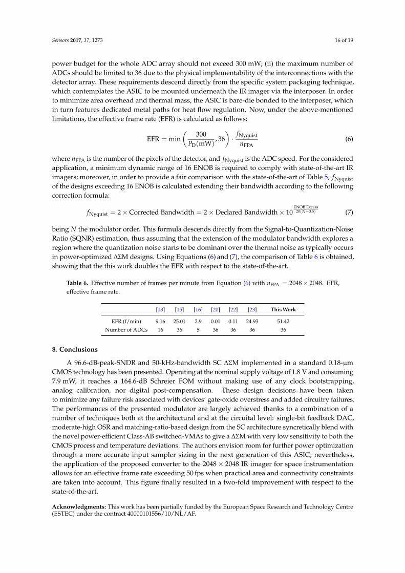
power budget for the whole ADC array should not exceed 300 mW; (ii) the maximum number ofADCs should be limited to 36 due to the physical implementability of the interconnections with thedetector array. These requirements descend directly from the specific system packaging technique,which contemplates the ASIC to be mounted underneath the IR imager via the interposer. In orderto minimize area overhead and thermal mass, the ASIC is bare-die bonded to the interposer, whichin turn features dedicated metal paths for heat flow regulation. Now, under the above-mentionedlimitations, the effective frame rate (EFR) is calculated as follows:
EFR = min(
300PD(mW)
, 36)· fNyquist
nFPA(6)
where nFPA is the number of the pixels of the detector, and fNyquist is the ADC speed. For the consideredapplication, a minimum dynamic range of 16 ENOB is required to comply with state-of-the-art IRimagers; moreover, in order to provide a fair comparison with the state-of-the-art of Table 5, fNyquist
of the designs exceeding 16 ENOB is calculated extending their bandwidth according to the followingcorrection formula:
fNyquist = 2×Corrected Bandwidth = 2×Declared Bandwidth× 10ENOB Excess
20(N+0.5) (7)
being N the modulator order. This formula descends directly from the Signal-to-Quantization-NoiseRatio (SQNR) estimation, thus assuming that the extension of the modulator bandwidth explores aregion where the quantization noise starts to be dominant over the thermal noise as typically occursin power-optimized ΔΣM designs. Using Equations (6) and (7), the comparison of Table 6 is obtained,showing that the this work doubles the EFR with respect to the state-of-the-art.
Table 6. Effective number of frames per minute from Equation (6) with nFPA = 2048× 2048. EFR,effective frame rate.
[13] [15] [16] [20] [22] [23] This Work
EFR (f/min) 9.16 25.01 2.9 0.01 0.11 24.93 51.42
Number of ADCs 16 36 5 36 36 36 36
8. Conclusions
A 96.6-dB-peak-SNDR and 50-kHz-bandwidth SC ΔΣM implemented in a standard 0.18-µmCMOS technology has been presented. Operating at the nominal supply voltage of 1.8 V and consuming7.9 mW, it reaches a 164.6-dB Schreier FOM without making use of any clock bootstrapping,analog calibration, nor digital post-compensation. These design decisions have been takento minimize any failure risk associated with devices’ gate-oxide overstress and added circuitry failures.The performances of the presented modulator are largely achieved thanks to a combination of anumber of techniques both at the architectural and at the circuital level: single-bit feedback DAC,moderate-high OSR and matching-ratio-based design from the SC architecture syncretically blend withthe novel power-efficient Class-AB switched-VMAs to give a ΔΣM with very low sensitivity to both theCMOS process and temperature deviations. The authors envision room for further power optimizationthrough a more accurate input sampler sizing in the next generation of this ASIC; nevertheless,the application of the proposed converter to the 2048× 2048 IR imager for space instrumentationallows for an effective frame rate exceeding 50 fps when practical area and connectivity constraintsare taken into account. This figure finally resulted in a two-fold improvement with respect to thestate-of-the-art.
Acknowledgments: This work has been partially funded by the European Space Research and Technology Centre(ESTEC) under the contract 40000101556/10/NL/AF.

Sensors 2017, 17, 1273 17 of 19
Author Contributions: In this research work, M.D. and S.S. were responsible for the design and the implementationof the ΔΣ-modulator presented under the tight surveillance of F.S.-G. R.J.E.J. provided the application backgroundand the system specifications along with constant feedback during the design phase of the circuit. Measurementsetup and tests were performed by S.S. and J.C. with the help E.P. The manuscript was written by F.S.-G., M.D.and R.J.E.J. and proofread by L.T., who also was the lead manager of the project.
Conflicts of Interest: The authors declare no conflict of interest.
References
1. Beletic, J.; Blank, R.; Gulbransen, D.; Lee, D.; Loose, M.; Piquette, E.; Sprafke, T.; Tennant, W.; Zandian, M.;Zino, J. Teledyne Imaging Sensors: Infrared imaging technologies for Astronomy & Civil Space.In Proceedings of the SPIE High Energy, Optical, and Infrared Detectors for Astronomy III, Marseille,France, 23 June 2008.
2. Bai, Y.; Bajaj, J.; Beletic, J.W.; Farris, M.C.; Joshi, A.; Lauxtermann, S.; Petersen, A.; Williams, G. TeledyneImaging Sensors: Silicon CMOS imaging technologies for X-ray, UV, visible and near infrared. In Proceedingsof the SPIE High Energy, Optical, and Infrared Detectors for Astronomy III, Marseille, France, 23 June 2008.
3. Loose, M.; Beletic, J.; Blackwell, J.; Garnett, J.; Wong, S.; Hall, D.; Jacobson, S.; Rieke, M.; Winters, G.The SIDECAR ASIC — Focal plane electronics on a single chip. In Proceedings of the SPIE Cryogenic OpticalSystems and Instruments XI, San Diego, CA, USA, 31 July 2005.
4. Finger, G.; Baker, I.; Downing, M.; Alvarez, D.; Ives, D.; Mehrgan, L.; Meyer, M.; Stegmeier, J.; Weller, H.J.Development of HgCdTe large format MBE arrays and noise-free high speed MOVPE EAPD arraysfor ground based NIR astronomy. In Proceedings of the International Conference on Space Optics, Tenerife,Spain, 7–10 October 2014.
5. De Borniol, E.; Rothman, J.; Salveti, F.; Feautrier, P. SWIR HgCdTe avalanche photodiode focal plane arrayperformance evaluation. In Proceedings of the International Conference on Space Optics, Tenerife, Spain,7–10 October 2014.
6. Knowles, P.; Hipwood, L.; Baker, I.; Weller, H. Advances in Selex ES infrared detectors for space and astronomy.In Proceedings of the International Conference on Space Optics, Tenerife, Spain, 7–10 October 2014.
7. Jorden, P.; Jerram, P.; Jordan, D.; Pratlong, J.; Robbins, M.K. e2v CCD and CMOS sensors and systemsdesigned for astronomical applications. Proc. SPIE 2016, 9915, doi:10.1117/12.2239429.
8. Guellec, F.; Boulade, O.; Cervera, C.; Moreau, V.; Gravrand, O.; Rothman, J.; Zanatta, J.-P. ROIC developmentat CEA for SWIR detectors: Pixel circuit architecture and trade-offs. In Proceedings of the InternationalConference on Space Optics, Tenerife, Spain, 7–10 October 2014.
9. Gao, P.; Dupont, B.; Dierickx, B.; Müller, E.; Verbruggen, G.; Gielis, S.; Valvekens, R. Cryogenix andradiation-hard ASIC for interfacing large format NIR/SWIR detector arrays. In Proceedings of the InternationalConference on Space Optics, Tenerife, Spain, 7–10 October 2014.
10. Påhlsson, P.; Steenari, D.; Øya, P.; Berge, H.K.O.; Meier, D.; Olsen, A.; Hasanbegovic, A.; Altan, M.A.;Najafiuchevler, B.; Talebi, J.; et al. NIRCA ASIC for the readout of focal plane arrays. In Proceedings of theSPIE Infrared Technology and Applications XLII, Baltimore, MD, USA, 17 April 2016.
11. Sutula, S.; Dei, M.; Terés, L.; Serra-Graells, F. Variable-Mirror Amplifier: A New Family of Process-IndependentClass-AB Single-Stage OTAs for Low-Power SC Circuits. IEEE Trans. Circuits Syst. I 2016, 63, 1101–1110.
12. Sutula, S.; Dei, M.; Terés, L.; Serra-Graells, F. A calibration-free 96.6-dB-SNDR non-bootstrapped 1.8-V7.9-mW delta-sigma modulator with class-AB single-stage switched VMAs. In Proceedings of the IEEEInternational Symposium on Circuits and Systems, Montreal, QC, Canada, 22–25 May 2016; pp. 61–64.
13. Nguyen, K.; Adams, B.; Sweetland, K.; Chen, H.; McLaughlin, K. A 106 dB SNR hybrid oversampling ADCfor digital audio. In Proceedings of the IEEE International Solid-State Circuits Conference, San Francisco,CA, USA, 10 February 2005; pp. 176–591.
14. Park, H.; Nam, K.; Su, D.K.; Vleugels, K.; Wooley, B.A. A 0.7-V 870-µW Digital-Audio CMOS Sigma-DeltaModulator. IEEE J. Solid-State Circuits 2009, 44, 1078–1088.
15. Wang, T.C.; Lin, Y.H.; Liu, C.C. A 0.022 mm2 98.5 dB SNDR hybrid audio delta-sigma modulator with digitalELD compensation in 28 nm CMOS. In Proceedings of the IEEE Asian Solid-State Circuits Conference,KaoHsiung, Taiwan, 10–12 November 2014; pp. 317–320.

Sensors 2017, 17, 1273 18 of 19
16. Yang, Y.; Chokhawala, A.; Alexander, M.; Melanson, J.; Hester, D. A 114-dB 68-mW chopper-stabilized stereomulti-bit audio A/D converter. In Proceedings of the IEEE International Solid-State Circuits Conference,San Francisco, CA, USA, 13 February 2003; pp. 56–477.
17. Brewer, R.; Gorbold, J.; Hurrell, P.; Lyden, C.; Maurino, R.; Vickery, M. A 100 dB SNR 2.5 MS/s Output DataRate ΔΣ ADC. In Proceedings of the IEEE International Solid-State Circuits Conference, San Francisco, CA,USA, 10 February 2005; pp. 172–173.
18. Morrow, P.; Chamarro, M.; Lyden, C.; Ventura, P.; Abo, A.; Matamura, A.; Keane, M.; O’Brien, R.; Minogue, P.;Mansson, J.; et al. A 0.18µm 102 dB-SNR Mixed CT SC Audio-Band ΔΣ ADC. In Proceedings of the IEEEInternational Solid-State Circuits Conference, San Francisco, CA, USA, 10 February 2005; pp. 178–592.
19. Silva, P.; Breems, L.; Makinwa, K.; Roovers, R.; Huijsing, J. An 118 dB DR CT IF-to-Baseband ΣΔ Modulatorfor AM/FM/IBOC Radio Receivers. In Proceedings of the IEEE International Solid-State Circuits Conference,San Francisco, CA, USA, 5–9 February 2006; pp. 151–160.
20. Chae, Y.; Souri, K.; Makinwa, K. A 6.3µW 20 b Incremental Zoom-ADC with 6 ppm INL and 1µVOffset. In Proceedings of the IEEE International Solid-State Circuits Conference, San Francisco, CA, USA,17–21 February 2013; pp. 276–277.
21. Bandyopadhyay, A.; Adams, R.; Khiem, N.; Baginski, P.; Lamb, D.; Tansley, T. A 97.3 dB SNR, 600 kHz BW,31 mW Multibit Continuous Time ΔΣ ADC. In Proceedings of 2014 Symposium on VLSI Circuits Digest ofTechnical Papers, Honolulu, HI, USA, 10–13 June 2014; pp. 1–2.
22. Xu, L.; Gönen, B.; Fan, Q.; Huijsing, J.; Makinwa, K.A.A. A 110 dB SNR ADC with ±30 V InputCommon-Mode Range and 8µV Offset for Current Sensing Applications. In Proceedings of the IEEEInternational Solid-State Circuits Conference, San Francisco, CA, USA, 22–26 February 2015; pp. 90–91.
23. Billa, S.; Sukumaran, A.; Pavan, S. A 280µW 24 kHz-BW 98.5 dB-SNDR chopped single-bit CT ∆ΣMAchieving <10 Hz 1/f Noise Corner without Chopping Artifacts. In Proceedings of the IEEE InternationalSolid-State Circuits Conference, San Francisco, CA, USA, 31 January–4 February 2016; pp. 276–277.
24. Murmann, B. ADC Performance Survey 1997–2015. Available online: http://web.stanford.edu/~murmann/adcsurvey.html (accessed on 1 June 2017).
25. Kim, M.; Ahn, G.; Hanumolu, P.; Lee, S.; Kim, S.; You, S.; Kim, J.; Temes, G.; Moon, U. A 0.9 V 92 dBDouble-Sampled Switched-RC ΔΣ Audio ADC. IEEE J. Solid-State Circuits 2006, 43, 1195–1206.
26. Rabii, S.; Wooley, B.A. A 1.8 V Digital-Audio Sigma-Delta Modulator in 0.8µm CMOS. IEEE J. Solid-StateCircuits 1997, 32, 783–796.
27. Crols, J.; Steyaert, M. Switched-OpAmp: An Approach to Realize Full CMOS Switched-Capacitor Circuits atVery Low Power Supply Voltages. IEEE J. Solid-State Circuits 1994, 29, 936–942.
28. Yao, L.; Steyaert, M.; Sansen, W. A 1-V, 1-MSs, 88-dB Sigma-Delta Modulator in 0.13-µm Digital CMOSTechnology. In Proceedings of 2005 Symposium on VLSI Circuits Digest of Technical Papers, Kyoto, Japan,16–18 June 2005; pp. 180–183.
29. De la Rosa, J.M. Sigma-Delta Modulators: Tutorial Overview, Design Guide, and State-of-the-Art Survey.IEEE Trans. Circuits Syst. I 2011, 58, 1–21.
30. Silva, J.; Moon, U.; Steensgaard, J.; Temes, G.C. A wideband low-distortion Delta-Sigma ADC topology.IEEE Electron. Lett. 2001, 37, 737–738.
31. Porrazzo, S.; Cannillo, F.; Hoof, C.V.; Cantatore, E.; van Roermund, A.H.M. A Power-Optimal DesignMethodology for High-Resolution Low-Bandwidth SC ∆Σ Modulators. IEEE Trans. Instrum. Meas. 2012,61, 2896–2904.
32. Wu, B.; Zhu, S.; Xu, B.; Chiu, Y. 15.1 A 24.7 mW 45 MHz-BW 75.3 dB-SNDR SAR-assisted CT ΔΣ modulatorwith 2nd-order noise coupling in 65 nm CMOS. In Proceedings of the IEEE International Solid-State CircuitsConference, San Francisco, CA, USA, 31 January–4 February 2016; pp. 270–271.
33. Dorrer, L.; Kuttner, F.; Santner, A.; Kropf, C.; Puaschitz, T.; Hartig, T.; Punzenberger, M. A ContinuousTime ∆Σ ADC for Voice Coding with 92 dB DR in 45 nm CMOS. In Proceedings of the IEEE InternationalSolid-State Circuits Conference, San Francisco, CA, USA, 3–7 February 2008; pp. 502–631.
34. Maghari, N.; Moon, U.K. A Third-Order DT ΔΣModulator Using Noise-Shaped Bi-Directional Single-SlopeQuantizer. IEEE J. Solid-State Circuits 2011, 46, 2882–2891.
35. Van de Plassche, R.J. CMOS Integrated Analog-to-Digital and Digital-to-Analog Converters; Kluwer AcademicPublishers: Dordrecht, The Netherlands, 2003.

Sensors 2017, 17, 1273 19 of 19
36. Malcovati, P.; Brigati, S.; Francesconi, F.; Maloberti, F.; Cusinato, P.; Baschirotto, A. Behavioral Modeling ofSwitched-Capacitor Sigma-Delta Modulators. IEEE Trans. Circuits Syst. I 2003, 50, 352–364.
37. Chen, J.; Ker, M. Circuit Performance Degradation of Sample-and-Hold Amplifier Due to Gate-OxideOverstress in a 130-nm CMOS Process. In Proceedings of the 2006 13th International Symposium on thePhysical and Failure Analysis of Integrated Circuits, Singapore, 3–7 July 2006; pp. 45–48.
38. Yukawa, A. A CMOS 8-Bit High-Speed A/D Converter IC. IEEE J. Solid-State Circuits 1985, 20, 775–779.39. Baruqui, F.; Petraglia, A. Linearly Tunable CMOS OTA With Constant Dynamic Range Using Source-Degenerated
Current Mirrors. IEEE Trans. Circuits Syst. II Express Briefs 2006, 53, 797–801.40. Aguirre, P.; Silveira, F. Bias Circuit Design for Low-Voltage Cascode Transistors. In Proceedings of the 19th
Annual Symposium on Integrated Circuits and Systems Design, Ouro Preto, Brazil, 28 August–1 September2006; pp. 94–97.
© 2017 by the authors. Licensee MDPI, Basel, Switzerland. This article is an open accessarticle distributed under the terms and conditions of the Creative Commons Attribution(CC BY) license (http://creativecommons.org/licenses/by/4.0/).