
A Reconfigurable Network-on-Chip Architecture for Optimal ...
21
HAL Id: hal-01054544 https://hal.inria.fr/hal-01054544 Submitted on 7 Aug 2014 HAL is a multi-disciplinary open access archive for the deposit and dissemination of sci- entific research documents, whether they are pub- lished or not. The documents may come from teaching and research institutions in France or abroad, or from public or private research centers. L’archive ouverte pluridisciplinaire HAL, est destinée au dépôt et à la diffusion de documents scientifiques de niveau recherche, publiés ou non, émanant des établissements d’enseignement et de recherche français ou étrangers, des laboratoires publics ou privés. Distributed under a Creative Commons Attribution| 4.0 International License A Reconfigurable Network-on-Chip Architecture for Optimal Multi-Processor SoC Communication Vincenzo Rana, David Atienza, Marco Domenico Santambrogio, Donatella Sciuto, Giovanni Micheli To cite this version: Vincenzo Rana, David Atienza, Marco Domenico Santambrogio, Donatella Sciuto, Giovanni Micheli. A Reconfigurable Network-on-Chip Architecture for Optimal Multi-Processor SoC Communication. 19th IFIP WG 10.5/IEEE International Conference on Very Large Scale Integration (VLSI-SoC), Oct 2008, Rhodes Island, India. pp.232-250, 10.1007/978-3-642-12267-5_13. hal-01054544
Transcript of A Reconfigurable Network-on-Chip Architecture for Optimal ...

HAL Id: hal-01054544https://hal.inria.fr/hal-01054544
Submitted on 7 Aug 2014
HAL is a multi-disciplinary open accessarchive for the deposit and dissemination of sci-entific research documents, whether they are pub-lished or not. The documents may come fromteaching and research institutions in France orabroad, or from public or private research centers.
L’archive ouverte pluridisciplinaire HAL, estdestinée au dépôt et à la diffusion de documentsscientifiques de niveau recherche, publiés ou non,émanant des établissements d’enseignement et derecherche français ou étrangers, des laboratoirespublics ou privés.
Distributed under a Creative Commons Attribution| 4.0 International License
A Reconfigurable Network-on-Chip Architecture forOptimal Multi-Processor SoC Communication
Vincenzo Rana, David Atienza, Marco Domenico Santambrogio, DonatellaSciuto, Giovanni Micheli
To cite this version:Vincenzo Rana, David Atienza, Marco Domenico Santambrogio, Donatella Sciuto, Giovanni Micheli.A Reconfigurable Network-on-Chip Architecture for Optimal Multi-Processor SoC Communication.19th IFIP WG 10.5/IEEE International Conference on Very Large Scale Integration (VLSI-SoC), Oct2008, Rhodes Island, India. pp.232-250, �10.1007/978-3-642-12267-5_13�. �hal-01054544�

A Reconfigurable Network-on-Chip
Architecture for Optimal Multi-Processor SoC
Communication
Vincenzo Rana1, David Atienza2,3, Marco Domenico Santambrogio1,Donatella Sciuto1, and Giovanni De Micheli4
1 Dipartimento di Elettronica e Informazione (DEI) - Politecnico di Milano,Via Ponzio 34/5, 20133 - Milano, Italy.E-mail: {rana, santambr, sciuto}@elet.polimi.it
2 Embedded Systems Laboratory (ESL) - Ecole Polytechnique Federale deLausanne (EPFL), ESL-IEL-STI-EPFL, Station 11, 1015-Lausanne, Switzerland.E-mail: [email protected]
3 Depto. de Arquitectura de Computadores y Automatica (DACYA) - UniversidadComplutense de Madrid (UCM), Avda. Complutense S/N, 28040-Madrid, Spain.
4 Integrated Systems Laboratory (LSI) - EPFL, LSI-ISIM-IC-EPFL, Station 14,1015-Lausanne, Switzerland.E-mail: [email protected]
Summary. Network-on-Chip (NoC) has emerged as a very promising paradigm fordesigning scalable communication architecture for Systems-on-Chips (SoCs). How-ever, NoCs designed to fulfill the bandwidth requirements between the cores of anSoC for a certain set of running applications may be highly sub-optimal for anotherset of applications. In this context, methods that can lead to versatility enhance-ments of initial NoC designs to changing working conditions, imposed by variablesets of executed real-life applications at each moment in time, are very importantfor designing competitive NoCs in industrial SoCs.
In this work, we present a run-time reconfigurable NoC framework based on thepartial dynamic reconfiguration capabilities of Field-Programmable Gate Arrays(FPGAs). This new NoC framework can dynamically create/delete express lines be-tween SoC components (implementing dynamically circuit-switching channels) andperform run-time NoC topology and routing-table reconfigurations to handle in-terconnection congestion, with a very limited performance overhead. Moreover, weshow in our experimental results that the addition of these dynamic reconfigurationcapabilities into basic NoCs using our framework only implies a very limited areaoverhead (around 10% on average) with respect to the initial NoC designs; thus, itcan bring great benefits when compared to traditional non-reconfigurable NoC de-sign approaches for worst-case bandwidth requirements in SoCs with many possiblesets of running applications.

2 V. Rana, D. Atienza, M. D. Santambrogio, D. Sciuto, G. De Micheli
Key words: Networks on Chips, Systems on Chips, Topology Reconfigura-tion, Express Lines, Dynamic Reconfiguration, FPGA.
1 Introduction and problem description
Latest applications ported to embedded systems (e.g., scalable video render-ing, communication protocols) demand a large computation power, while mustrespect other critical embedded design constraints, such as, short time-to-market, low energy consumption or reduced implementation size.
Thus, embedded systems are complex Systems-on-Chip (SoCs) that con-sist of a large number of components, such as, processing elements, storagedevices and even reconfigurable devices, such as Field-Programmable Gate Ar-rays (FPGAs), to enhance the flexibility of final SoCs to be used in differentenvironments [15, 5]. Nevertheless, one of the most critical areas of MPSoCdesign is the definition of the suitable interconnect subsystem for all theseSoC components, due to architectural and physical scalability concerns [3]. Infact, traditional shared bus interconnects are relatively easy to design, but donot scale well for latest and forthcoming SoC consumer platforms.
In order to cope with the large communication demands of such SoCs, theuse of modular and scalable Networks-on-Chips (NoCs) has been proposed [3].Then, designing custom-tailored NoC interconnects that satisfy the perfor-mance and design constraints of the SoC for all the different combinationsof possible executed applications is a key goal to achieve optimal commercialproducts [13, 2]. However, as general-purpose processor cores are used to runsoftware tasks of different applications in SoCs, the communication betweenthe cores cannot be precharacterized and fully optimized, since the applicationprocesses can be mapped differently to the cores, typically with the support ofthe compiler. Thus, to provide predictable performance of the NoC, the band-width capacity of the different links must be sufficient to support the peakrate of traffic on the links of the possible different mappings of the tasks ontothe final SoC. Otherwise, the network might experience traffic congestion andthe latency for the traffic streams and, hence, the interconnect performancewill become unacceptable, which needs to be avoided to provide appropriateconsumer devices. As a result, NoCs designs that guarantee worst-case band-width conditions of SoC operation with multiple concurrent application oftenleads to over-sized topologies and links on regular operation of the SoC. In thiscontext, the development of new methods and frameworks that increase therun-time versatility of initial static NoC designs to adapt to different workingconditions, originated by the diversity of sets of applications at each moment,is an important research area in the NoC domain.
In this paper we introduce a novel run-time reconfigurable NoC framework,which exploits the partial dynamic reconfiguration capabilities of FPGAs toadapt at run-time the implemented NoC interconnect to the specific work-ing requirements of the final SoC at each moment in time. In particular, the

Reconfigurable Network-on-Chip Architecture 3
proposed NoC framework is able to reduce the latency of interconnecting theincluded SoC components by dynamically establishing or deleting a numberof dedicated point-to-point connections between them (or express lines in theNoC literature [3]), which is particularly suited for video and audio stream-ing. Thus, circuit-switching communication can be dynamically configured inthe SoC. In addition, our framework enables a fast dynamic reconfigurationof routing tables (few cycles) and overall NoC topologies (few milliseconds),which provides new promising means to overcome congestion and consequentlyprovide more reliable and high-performance NoC designs. Furthermore, ourexperimental results show that the addition of the dynamic reconfigurationcapabilities in basic NoCs using our framework only involves limited area over-heads (around 10% on average) with respect to initial NoC designs withoutreconfiguration capabilities. Hence, the proposed reconfigurable NoC frame-work is viable to be considered in commercial designs of SoCs.
It is possible to fully exploit the reconfigurable NoC proposed in this workin order to establish dedicated (among 2 or more switches of the network)and long (circuit-switching) communication channels among the cores of thereconfigurable system. This can be really useful, for instance, in the case ofaudio and video streaming that have to be dynamically carried out at run-time, without the possibility to obtain detailed information at design time.In this case, in fact, the proposed approach enables to dynamically reconfig-ure the communication infrastructure accordingly to the need that arise atrun-time, in order to meet both latency and throughput requirements. Thisis possible since the reduction of the number of hops between two switchesdirectly decreases the latency between them and the introduction of a newexpress line in the topology directly increases the overall throughput of theNoC.
The rest of the paper is organized as follows. In Section 2 we overviewprevious work in the field on reconfigurable NoCs. Then, in Section 3 weintroduce our reconfigurable NoC architecture, spanning from the includedbasic NoC architecture to the additional components to enable the NoC Next,in Section 4 we discuss the major reconfiguration capabilities and methods toimplement them in the proposed adaptive NoC framework. Later, in Section 5we present the area, performance and latency evaluation of the reconfigurationcapabilities of our framework in a real implementation on a large commercialFPGA implementing a multi-processor SoC. Finally, in Section 6 we draw themain conclusions of this work.
2 State of the art
In recent years, several works focused their attention into the definition ofa reconfigurable communication infrastructure for reconfigurable Systems-on-chip. For instance, in [11] the authors present a methodology for developingdynamic network reconfiguration processes, but they define a reconfiguration

4 V. Rana, D. Atienza, M. D. Santambrogio, D. Sciuto, G. De Micheli
just as the change from one routing function to another while the network isup and running. For this reason they present a theoretical work based on thelimiting assumption (not valid in the approach presented in this paper) thatthe network topology can be considered fixed (like in [7]).
The work presented in [6] describes an integrated modeling, simulationand implementation tool for reconfigurable NoCs. The work is based on theoptimization of a single given application and no details are given about thereconfigurable architecture of the NoC and about reconfiguration mechanisms.In addition to this, flow control is not supported and the proposed NoCs arequite expensive in terms of area usage (2733 slices, around 30% of the totalslices of a Xilinx Virtex II Pro XC2VP20 device), for a 2x2 torus running at85 MHz, while the proposed approach, with a lower area usage, allows thecreation of a 3x3 mesh running at 170 MHz.
In [1], a dynamically reconfigurable NoC architecture is presented. ThisNoC can be dynamically configured with respect to routing, switching anddata packet size, but all the required resources have to be allocated at designtime, since at run-time it is only possible to dynamically change a limitednumber of parameters. A similar approach can be found in [10], where theproposed NoC can be configured at run-time, but only with respect to mem-ories content, resources addressing and control parameters, while topology,buffers size and port connections have to be determined at design time.
In [9], a scalable dynamic NoC for dynamically reconfigurable FPGAs(CuNoC) is presented. The main idea behind CuNoC approach is to fill thewhole reconfigurable devices with very small communication units called CUs,that can establish a communication channel between two different cores. Themain drawback of this approach is, in addition to the huge power consumption,the high latency for each communication. In fact, the number of hops requiredfor a communication is very high on average, as each packet has to passthrough a high number of CUs (each one having a latency of 2 clock cycles),since it is not possible neither to define a custom topology nor to configureexpress lines between CUs. Furthermore, if an obstacle is present betweentwo cores that need to communicate, it is necessary to go around it, whichincreases the number of hops of each packet.
In [14] the authors present CoNoChi, that is an adaptable NoC for dynam-ically reconfigurable hardware design. The reconfigurable device is divided ina matrix, and each cell of this matrix can hold either a computational moduleor a communication element (a switch or point-to-point interconnect). Sinceit is not possible to pass through a computational module, each communica-tion channel has to go around all the computational elements placed on thereconfigurable device; thus, express lines cannot be configured at run-time. Inaddition to this, the area requirement for a single switch is very high, as itvaries from 463 to 493 slices (around 5% of a XC2VP20 device). Then, theworking frequency is quite low (it ranges from 66 to 73 MHz) and the actuallatency of each switch is 5 clock cycles, which can be a significant penalty forinterconnection mechanisms nowadays.

Reconfigurable Network-on-Chip Architecture 5
3 The proposed reconfigurable architecture
3.1 Reconfiguration support
In order to configure an FPGA with the desired functionality, we need to useone or more bitstreams. A bitstream is a binary file in which configurationinformation for a particular Xilinx device is stored, that is where all the datato be copied on to the configuration SRAM cells, the configuration memory,are stored, along with the proper commands for controlling the chip func-tionalities. Therefore Virtex devices, such as Virtex II Pro and Virtex 4, areconfigured by loading application specific data into their configuration mem-ory, as shown in Figure 1. On the Virtex FPGAs the configuration memory is
Fig. 1. Configuration memory setup
segmented into frames. Virtex devices are partially reconfigurable and a frameis the smallest unit of reconfiguration. According to the device, this elementcan span the entire length of the FPGA, such as in the Virtex II Pro context,or just part of it, as in Virtex 4 devices. The number of frames and the bitsper frame are specific for each device family. The number of frames is propor-tional to CLB width. Bitstreams can be either partial or full. A full bitstreamconfigures the whole configuration memory and is used for static design or atthe beginning of the execution of a dynamic reconfiguration system, to definethe initial state of SRAM cells. Partial bitstreams configure only a portion ofthe device and are one of the end products of any partial reconfiguration flow.

6 V. Rana, D. Atienza, M. D. Santambrogio, D. Sciuto, G. De Micheli
FPGAs provide different means for configuration, under the form of differ-ent interfaces to the configuration logic on the chip. There are several modesand interfaces to configure a specific FPGA family, among them the the IEEE1149.1 Joint Test Action Group (JTAG) download cable (the one used inthis work), the SelectMAP interface, for daisy-chaining the configuration pro-cess of multiple FPGAs, configuration loading from PROMs or compact flashcards, microcontroller-based configuration, an Internal Configuration AccessPort (ICAP) and so on, depending on the specific family. The ICAP providesan interface which can be used by internal logic to reconfigure and read backthe configuration memory. In every FPGA a configuration logic is built on thechip, with the purpose of implementing the different interfaces for exchangingconfiguration data and to interpret the bitstream to configure the device. Aset of configuration registers defines the state of this configuration logic ata given moment in time. Configuration registers are the memory where thebitstream file has direct access. Actual configuration data is first written bythe bitstream into these registers and then copied by the configuration logicon the configuration SRAMs.
3.2 Architecture description
As previously hinted, the communication infrastructure of the proposed ar-chitecture is based on the NoC paradigm. Furthermore, in order to exploita 2-layered approach, in which the computational layer is completely decou-pled from the communication layer, the proposed reconfigurable architecturemainly consists of two different parts: a static part and a reconfigurable part.
The static part consists of all the computational elements and the net-work interfaces. On the one hand, computational elements can be furtherdivided into two categories. The first one consists of masters, that are the ac-tive components of the system, such as microprocessors (either a soft-core, asa MicroBlaze, or a hard-core as a PowerPC), that can initialize new transac-tions on the network (deployed in the communication layer); these componentsare connected to the communication infrastructure through NI initiators (seeFigure 2). The second one consists of slaves, such as memories, that repre-sent the components that act in a passive mode, by receiving and answeringtransaction coming from active elements; these components are connected tothe communication infrastructure through NI targets (see Figure 2).
The static part consists of all the computational elements and the net-work interfaces. Computational elements can be further divided into masters(that are the active components of the system, such as microprocessors, thatcan initialize new transactions on the network and that are connected to thecommunication infrastructure through NI initiators, as shown in Figure 2)and slaves (such as memories, that represent the components that act in apassive mode, by receiving and answering transaction coming from active el-ements, and that are connected to the communication infrastructure throughNI targets, as shown in Figure 2).

Reconfigurable Network-on-Chip Architecture 7
Static Reconfigurable
MB
PPC
Slave
NIInitiator
NITarget
NIInitiator
Static
MB
Slave
NIInitiator
NITarget
OPB
OPB
PLB
OPB
PLB
NoC SlaveNI
TargetPLB
NoC protocol
OPB / PLB bus
Busmacro
Fig. 2. Interfaces between static and reconfigurable parts
The reconfigurable part is composed by all the reconfigurable elements,used to adapt at run-time the structure of the system implemented on theFPGA. These elements can be either computational components or elementsused to update the communication infrastructure. Network interfaces towardthe communication infrastructure can implement bridges between On-chipPeripheral Bus (OPB), Processor Local Bus (PLB) or Open Core Protocol(OCP) and the network protocol, as shown in Figure 2. The only part of net-work interfaces (both initiator and target network interfaces) that has to bemodified at run-time are routing tables, that are used to dynamically changethe routing of packets on the network. Thus, all the network interfaces havebeen placed into the static part of the system and routing tables have beendeployed on BRAM blocks. In this way it is possible to dynamically mod-ify routing tables by changing the content of BRAM blocks at run-time, asdescribed in Section 4.1.
This architectural solution enables connecting the static parts to the re-configurable ones by using network interfaces that are considerably thinner ofthe ones used within the static part of the system. Regarding this static part,the used interconnect can be either OPB and PLB buses, or on an ad-hocpoint-to-point communication infrastructure, as shown in Figure 2.
4 Reconfiguration features
Each reconfigurable part of the system can be dynamically reconfigured atrun-time to modify either a part or the whole underlying communication in-frastructure. This reconfiguration can be done by the reconfiguration con-troller (see Figure 3), which is a master component present on the static part,trough partial reconfiguration operations.
The reconfiguration controller is connected both to the external dynamicmemory (DDR) interface and to the ICAP interface through the OPB bus.

8 V. Rana, D. Atienza, M. D. Santambrogio, D. Sciuto, G. De Micheli
Static
MB
PPC
Slave
Initiator
Target
Initiator
OPB
OPB
PLB
BRAM block
BRAM block
BRAM block
Read
Read
Read
Reconfiguration controller ICAP interface
OPB
Memory (DDR) interface
Fig. 3. A static part with a reconfiguration controller
The DDR memory is used to store partial bitstreams that can be used toreconfigure at run-time the reconfigurable device. In order to perform a re-configuration process, the reconfiguration controller has to read the desiredbitstream from the memory and to pass it to the ICAP interface, connectedto the ICAP component, that will take care of the physical reconfigurationprocess. The reconfiguration controller is aware of both the current configu-ration of the reconfigurable NoC (routing tables, topology and express lines)and the current communication requirements, such as the cores that have tocommunicate and the required bandwidth and latency. In this way, the con-troller is able to adapt the underlying communication infrastructure in orderto satisfy communication requirements, even when they vary at run-time.
As previously hinted, the proposed reconfigurable NoC can be dynami-cally adapted to the current operating scenario by modifying network inter-faces routing tables at run-time, as described in Section 4.1. Furthermore, adynamic change into the proposed reconfigurable NoC can also involve eitherthe connection among switches (by inserting or removing express lines) or thewhole topology, as described in Section 4.2.
4.1 Path reconfiguration
Storing routing tables in BRAM blocks allows to dynamically change them atrun-time in two different ways. The first solution is to write the new routingtable with a simple write operation on the selected BRAM block. This writeoperation can be performed by the reconfiguration controller, that has to man-age both the physical reconfiguration and the modification of BRAMs content,

Reconfigurable Network-on-Chip Architecture 9
since routing tables have to be always consistent with respect to the currenttopology of the network. Using the reconfiguration controller for writing onBRAM blocks makes it necessary to directly connect it to each BRAM block,increasing the complexity and the area usage of the reconfigurable system.
A second solution consists of performing a partial dynamic reconfigurationof BRAM blocks, as described in [12]. This reconfiguration has to be performedby the reconfiguration controller, but in this case there is no need to directlyconnect it to each BRAM block, since these elements are updated by thecontroller using the configuration memory; thus, no area overhead is intro-duced. Performing this kind of reconfiguration enables dynamically changingBRAM blocks content (routing tables), in order to change the functionalityof the network interfaces at run-time, while leaving unaltered all the logicimplementing the functionality of the system; this allows a complete decou-pling between routing tables and the logic that implements both the staticand the reconfigurable components. The main drawback of this solution is theincrement of the time overhead of the network reconfigurations, as stated inSection 5.
4.2 Express lines and topology reconfiguration
In order to exploit express lines reconfiguration, it is necessary to define areconfigurable architecture that consists of several reconfigurable parts, inwhich it is possible to deploy the switches of the NoC. This can be done bymeans of the Early Access Partial Reconfiguration design flow [8] defined byXilinx. This flow allows to implement a reconfigurable architecture containingan arbitrary set of reconfigurable regions (which shape is a rectangle spanningthe whole height of the reconfigurable device, for FPGA of Virtex, Virtex IIand Virtex II Pro families, or an arbitrary rectangle for FPGA of Virtex IVand Virtex V families). Both the static architecture and each reconfigurablemodule, which need to be placed in a single reconfigurable region, can be con-figured on the target device by using a specific bitstream, namely, a completebitstream for the static part and a partial bitstreams for the reconfigurablemodules. All the bitstreams generated by this flow are the ones used by thepreviously described reconfiguration controller to change the current configu-ration of the system; in other words, the reconfiguration controller is able toselect a partial bitstream to be configured on the device in order to changethe underlying communication infrastructure. In particular, if an express linehas to be placed between to switches that belong to the same reconfigurableregion, the reconfiguration controller has to configure a new version of the re-configurable region in which the two switches are directly connected (througha new connection). A similar procedure can be applied to completely changethe topology of the NoC. In this case, a deeper modification of the selectedreconfigurable part is needed, in order to make it possible to change the num-ber and the kind of the switches of the same reconfigurable part (and thus ofthe whole NoC).

10 V. Rana, D. Atienza, M. D. Santambrogio, D. Sciuto, G. De Micheli
The number of express lines that can be established between two reconfig-urable regions has to be decided at design-time, since each bus-macro (whichenables to establish a single reliable communication channel among differentregions) has to be placed during the place and route phase of the architecture.Furthermore, the maximum number of express lines, which is always in theorder of tens for FPGA of Virtex II, Virtex II Pro, Virtex IV and Virtex Vfamilies, is limited by the amount of available resources along the edge amongreconfigurable and static regions; hence, it strictly depends both on the targetreconfigurable device and on the shape of each reconfigurable or static region.
5 Experimental results
This section presents a set of experimental results that validate the perfor-mance of the proposed reconfigurable architecture. These results have beenachieved by implementing the proposed reconfigurable architectures on a Xil-inx Virtex II Pro (XC2VP20) device. However, the same approach can beeasily adapted to another device, even in a different family, such as Virtex IVand Virtex V.
5.1 Routing tables reconfiguration analysis
Regarding routing tables reconfiguration, it can be performed in a fewclock cycles if it is performed with a simple write operation. In particular,if routing tables reconfiguration is performed directly by the reconfigurationcontroller, the latency of the reconfiguration is only 2 clock cycles (0.02 µs
at 100 MHz). On the other hand, by performing a partial dynamic config-uration of BRAMs, even if both the area and the complexity overheads arenot increased, the latency of the reconfiguration is considerably higher (2.24ms at 100 MHz). Table 1 summarizes all the experimental results related todynamic routing table reconfiguration.
Table 1. Routing tables reconfiguration experimental results
Reconfiguration Timing overhead Timing overhead Area Complexitymodel (Clock cycles) (ms) @ 100 MHz overhead increment
Write operation(reconfiguration controller) 2 0.00002 yes yes
Partial dynamicreconfiguration of asingle BRAM block 224242 2.24 no no

Reconfigurable Network-on-Chip Architecture 11
5.2 Express lines and topology reconfiguration analysis
Even if express lines reconfiguration and topology reconfiguration canbe used in order to achieve different modifications of the underlying network,from the timing overhead point of view, they are characterized by the samevalues, because the time required to reconfigure a reconfigurable region isexactly the same in both cases. Since the reconfiguration on Xilinx Virtex IIPro devices can only be performed with a 1D approach, the reconfigurationlatency is directly related to the width of the reconfigurable region that has tobe reconfigured. For instance the reconfiguration latency for a 4 slices widthregion, which can be filled with up to two switches, is around 21 ms, while a20 slices width region, which can include up to ten switches, requires around104 ms, as shown in Table 2,
Table 2. Express lines and topology reconfiguration results
Width of the Reconfiguration Bitstreamreconfigurable slot (slices) latency (ms) size (Kb)
4 21 32
6 30 46
8 41 62
10 52 78
12 63 94
14 75 112
16 80 120
18 93 140
20 104 156
In particular, regarding express lines reconfiguration, it can be ex-ploited both to reduce the traffic on a part of the NoC and to decrease thelatency between two switches. In order to better explain how it is possible todynamically configure express lines on the proposed reconfigurable architec-ture, let us consider a simple 3x3 mesh network, similar to the one presentedin Figure 4 (A). Without any express line, if the MicroBlaze 0 (MB 0) has tocommunicate with Slave 4, 3 hops (a path to a destination on a network canbe considered as a series of hops, through switches) are necessary in order togo from Switch 0 (to which MB 0 is connected through an initiator networkinterface) to Switch 5 (to which Slave 4 is connected through a target networkinterface). To this end, each packet has to pass, for instance, through Switch1 and Switch 2, in order to reach its final destination. In a similar way, thecommunication between PPC 0 and Slave 3 requires at least 2 hops (betweenSwitch 6 and Switch 8), since each packet has also to pass through Switch 7.
In the proposed reconfigurable architecture, it is possible to configure adirect connection between the port 3 of Switch 0 and the port 4 of Switch 5,
12 V. Rana, D. Atienza, M. D. Santambrogio, D. Sciuto, G. De Micheli
Switch0
Switch1
Switch2
Switch3
Switch4
Switch5
Switch6
Switch7
Switch8
Initiator
Target
Initiator
Initiator
Target
Target
Target Initiator
Initiator
Target
3
20
1
3
20
1
3
20
1
3
20
1
3
20
1
3
20
1
2
0
1
2
10
2
10
3
3
3
MB 0
Slave 0
PPC 0
Slave 1
Slave 2
MB 2
Slave 3
MB 3
Slave 4
MB 1
4
4
Static 0 Reconfigurable 0 Static 1 Reconfigurable 1 Static 2 Reconfigurable 2 Static 3
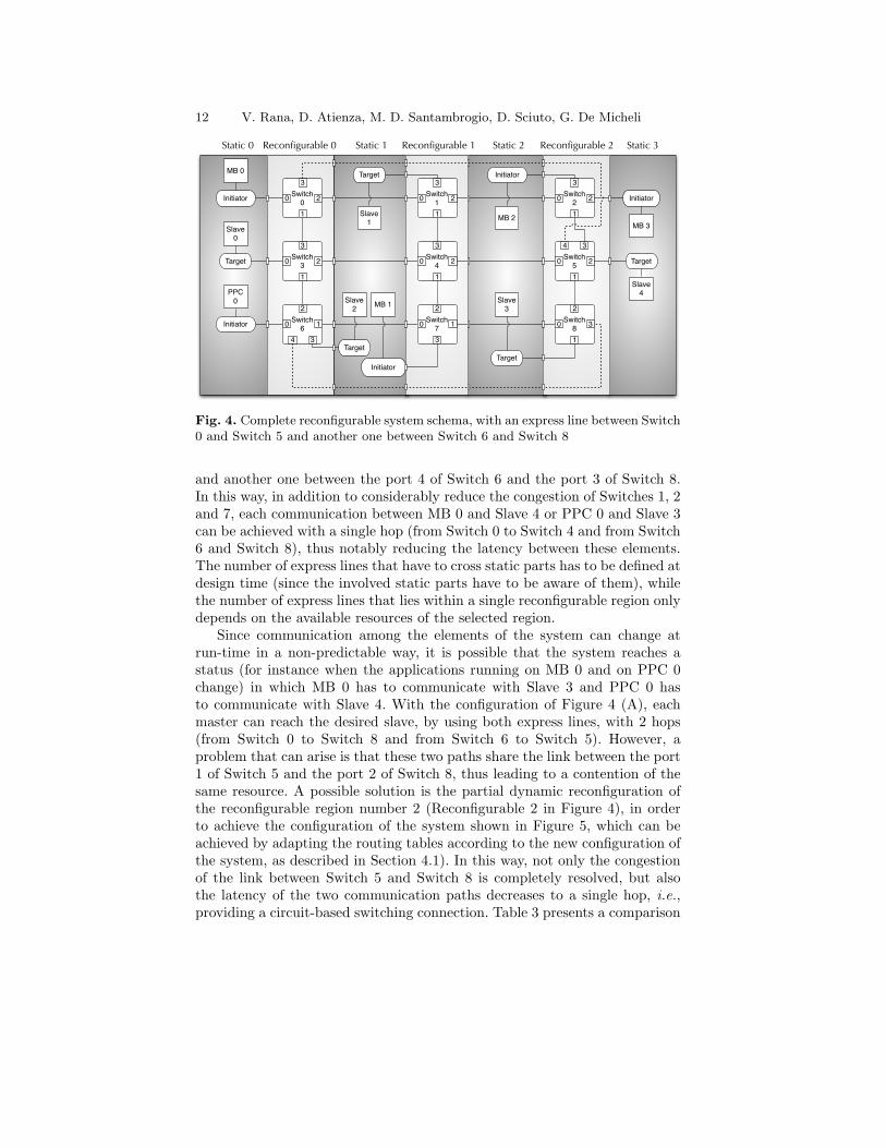
Fig. 4. Complete reconfigurable system schema, with an express line between Switch0 and Switch 5 and another one between Switch 6 and Switch 8
and another one between the port 4 of Switch 6 and the port 3 of Switch 8.In this way, in addition to considerably reduce the congestion of Switches 1, 2and 7, each communication between MB 0 and Slave 4 or PPC 0 and Slave 3can be achieved with a single hop (from Switch 0 to Switch 4 and from Switch6 and Switch 8), thus notably reducing the latency between these elements.The number of express lines that have to cross static parts has to be defined atdesign time (since the involved static parts have to be aware of them), whilethe number of express lines that lies within a single reconfigurable region onlydepends on the available resources of the selected region.
Since communication among the elements of the system can change atrun-time in a non-predictable way, it is possible that the system reaches astatus (for instance when the applications running on MB 0 and on PPC 0change) in which MB 0 has to communicate with Slave 3 and PPC 0 hasto communicate with Slave 4. With the configuration of Figure 4 (A), eachmaster can reach the desired slave, by using both express lines, with 2 hops(from Switch 0 to Switch 8 and from Switch 6 to Switch 5). However, aproblem that can arise is that these two paths share the link between the port1 of Switch 5 and the port 2 of Switch 8, thus leading to a contention of thesame resource. A possible solution is the partial dynamic reconfiguration ofthe reconfigurable region number 2 (Reconfigurable 2 in Figure 4), in orderto achieve the configuration of the system shown in Figure 5, which can beachieved by adapting the routing tables according to the new configuration ofthe system, as described in Section 4.1). In this way, not only the congestionof the link between Switch 5 and Switch 8 is completely resolved, but alsothe latency of the two communication paths decreases to a single hop, i.e.,providing a circuit-based switching connection. Table 3 presents a comparison

Reconfigurable Network-on-Chip Architecture 13
among the latency introduced by the NoC of Figure 4, the NoC of Figure 5and a NoC in which express lines are not taken into account.
Switch0
Switch1
Switch2
Switch3
Switch4
Switch5
Switch6
Switch7
Switch8
Initiator
Target
Initiator
Initiator
Target
Target
Target Initiator
Initiator
Target
3
20
1
3
20
1
3
20
1
3
20
1
3
20
1
3
20
1
2
0
1
2
10
2
10
3
3
3
MB 0
Slave 0
PPC 0
Slave 1
Slave 2
MB 2
Slave 3
MB 3
Slave 4
MB 1
4
4
Static 0 Reconfigurable 0 Static 1 Reconfigurable 1 Static 2 Reconfigurable 2 Static 3
Fig. 5. Complete reconfigurable system schema, with an express line between Switch0 and Switch 8 and another one between Switch 6 and Switch 5
Table 3. Latency introduced by the NoC
Source Target Figure 4 Figure 5 Mesh without express lines(number of hops) (number of hops) (number of hops)
MB 0 Slave 0 2 2 2
MB 0 Slave 1 2 2 2
MB 0 Slave 2 3 3 3
MB 0 Slave 3 3 2 5
MB 0 Slave 4 2 3 4
PPC 0 Slave 0 2 2 2
PPC 0 Slave 1 4 4 4
PPC 0 Slave 2 1 1 1
PPC 0 Slave 3 2 3 3
PPC 0 Slave 4 3 2 4
An important consideration is that, while the partial reconfiguration of thereconfigurable region 2 is performed, the communication among other partsof the system does not need to be interrupted, as long as it does not affectthe region that is reconfigured. For instance, if MB 1 has to communicate

14 V. Rana, D. Atienza, M. D. Santambrogio, D. Sciuto, G. De Micheli
with Slave 0 or Slave 1, this communication can take place even during thereconfiguration of the reconfigurable region 2.
The physical implementation of the previously presented architecture isshown in Figure 6, where A indicates the static part, while B, C and D rep-resent the three reconfigurable regions (which width is, respectively, 16, 20,and 14 slices - the 18%, 22% and 16% of a XC2VP20 device). All the recon-figurable regions have been filled with three switches each one, in order toimplement the previously presented 3x3 mesh.
Fig. 6. Physical implementation of the reconfigurable 3x3 mesh
Table 4 shows the experimental results regarding area usage and recon-figuration latency of the proposed architecture on a XC2VP20 device. Thebus-macro overhead consists of 288 slices, while the complete 3x3 mesh re-quires 2237 slices. Thus, the overhead introduced by the proposed approachrepresents the 10% (on average) of the initial NoC.
Furthermore, it is possible to configure at least two express lines in theimplemented architecture, and since each express line of the presented designhas a latency lower than 4 ns, it is possible to exploit each direct connectionwithin a single clock cycle at 100 MHz (while the latency required by theconnection passing through Switch 1, Switch 2 and Switch 5 is greater then40 ns, i.e., 4 clock cycles).
On the other hand, a topology reconfiguration can be exploited on thesame architecture in order to adopt a specific NoC for each application that

Reconfigurable Network-on-Chip Architecture 15
Table 4. Area usage and reconfiguration latency results
Area usage Area Reconfiguration(slices) usage (%) latency (ms)
Reconfigurableregion B 800 8.6 80
Reconfigurableregion C 637 6.9 104
Reconfigurableregion D 800 8.6 75
Complete3x3 mesh 2237 24.1 259
Bus-macrooverhead 288 3.1
has to be run on the system. In order to completely change the topology of theNetwork-On-Chip, a deeper modification of the selected reconfigurable partis needed, since both the number and the kind of the switches of the samereconfigurable part can be changed. As an example, let us consider that MB0 has to communicate with both Slave 0 and Slave 2 with the lowest latencypossible. In order to satisfy this strict requirement, it is necessary to changethe original topology of the network, by altering the mesh (in particular, theoriginal reconfigurable slot number 0 shown in Figure 7 A) as shown in Figure7 B. In the reconfigurable module shown in Figure 7 B, in fact, MB 0, Slave0 and Slave 2 are all connected to Switch 0, in order to make it possible forMB 0 to reach Slave 0 and Slave 2 without any hop.
Another case in which a reconfiguration of the topology can lead to meetcommunication requirements is, for instance, when both MB 0 has to commu-nicate with Slave 2 and MB 1 has to communicate with Slave 0 with the lowestlatency possible. In this case, the reconfigurable module shown in Figure 7 Ccan be configured in the reconfigurable slot number 0 (Reconfigurable 0), inorder to connect both MB 0 and Slave 2 to Switch 0, and MB1 and Slave 0 toSwitch 6. Thanks to this reconfiguration of the topology it is possible to estab-lish both the required communication channels without any overhead in termsof hops between switches, since all the components that has to communicatebetween them have been connected to the same switch.
We have validated the proposed approach with three different versions ofreal-life SoC benchmarks, namely, a video processing application of 32 cores(A), a Video Object Plane Decoder of 34 cores (B) and an image processingapplication of 23 cores (C). We refer the readers to [4] for the communicationcharacteristics of these benchmarks. As shown in Figure 8, if these differentapplications have to deployed on the same system, it is possible to employeither a static network or three specific NoCs, each one designed ad-hoc forthe particular application. The second choice can be adopted if the time in-

16 V. Rana, D. Atienza, M. D. Santambrogio, D. Sciuto, G. De Micheli
Switch
0
Switch
3
Switch
6
3
20
1
3
20
1
2
10
3
4
Reconfigurable 0
Switch
0
Switch
6
3
20
1
2
10
3
Reconfigurable 0
4
Switch
0
Switch
6
3
20
1
2
10
3
Reconfigurable 0
4
B) C)A)
Fig. 7. Alteration of the original mesh topology through the reconfiguration of theoriginal reconfigurable slot 0 (Reconfigurable 0) (A) with two different versions ofthe subnetwork (B and C)
terval that occurs between two consecutive applications is greater than thetime overhead required by the reconfiguration process; thus, it is possible totransparently change the underlying NoC.
A B C
Static NoC
Application
Static CI
NoC 1 NoC 2Proposed CI NoC 3
Time1 2 3 4 5 6 7
X Y
Fig. 8. Temporal evolution of a generic system
In order to test the application of our dynamically reconfigurable frame-work in this context, we have developed a static NoC and three specific onesfor each of the three aforementioned SoC benchmarks application. As shownin Figure 9, the static NoC consists of 6 switches (1 switch of 8x8, 2 switchesof 9x9, 2 switches 10x10 and 1 switch of 11x11), whileboth NoC 1 (for ap-plication A) and NoC 3 (for application C) consists of 4 switches (3 switchesof 10x10 and 1 switch of 11x11) and NoC 2 (for application B) consists of4 switches (1 switch of 10x9, 2 switches of 10x10 and 1 switch of 10x11), asshown in Figure 10. The static NoC option, as shown in Table 5, is character-ized by a higher area usage, a higher average power consumption (evaluated

Reconfigurable Network-on-Chip Architecture 17
as proposed in [2]) and a higher average latency, with respect to the three ad-hoc NoCs specifically designed for each application. Using the specific NoCs,it can be reported reductions of 34% in latency and 24% in power consump-tion. Finally, the overall latency for the reconfiguration of the NoC to be usedat run-time is very limited, making it applicable in real-life scenarios whereapplications are switched dynamically by users.
Fig. 9. Topology of the static NoC
As previously hinted, the reconfiguration latency of a reconfigurable regionstrictly depends on its size. For instance, the reconfiguration latency for a 4slices width region (that can be filled with up to two switches) is around 21ms, while a 20 slices width region (that can be filled with up to ten switches)requires around 104 ms.
Table 5. Specific NoCs experimental results
NoC Number Average latency Average powerof switches (clock cycles) consumption (mW)
Static NoC 6 5.96 278.021
NoC 1 4 3.9 211.789
NoC 2 4 4 204.308
NoC 3 4 4.07 216.519

18 V. Rana, D. Atienza, M. D. Santambrogio, D. Sciuto, G. De Micheli
Fig. 10. Topology of the NoC 2
Finally, Table 6 presents a comparison among state-of-the-art solutionsand our approach, which shows the clear benefits of our approach regard-ing area overhead reduction, timing performance improvements and enhance-ments of the reconfiguration features.
6 Conclusions
NoCs have been proposed as a very promising scalable communication paradigmSoCs. However, methods that provide versatility enhancements of initial NoCdesigns to changing working conditions, imposed by variable sets of executedapplications at run-time, are key to design competitive NoCs in industrialSoCs. In this work we have presented a novel NoC reconfigurable frameworkthat can reconfigure the NoC topology at run-time, as well as enabling pathreconfiguration and express lines creation/removal, while introducing an over-head on average of 10% of an initial static NoC design. Moreover, our exper-imental results have shown that in the proposed framework, on average, areconfigurable switch only occupies 41% of the slices needed by a CoNoChiswitch, the state-of-the-art reconfigurable NoC approach, whereas our recon-

Reconfigurable Network-on-Chip Architecture 19
Table 6. Area overhead, timing performance and features comparison among stateof the art solutions and the proposed approach
Approach CuNoC CoNoChi Proposed([9]) ([14]) work
Switch size (slices) from 72 to 491 from 363 to 493 from 86 to 267
Communication All theinfrastructure available 2727 forsize (slices) resources NA a 3x3 mesh
Frequency (MHz) from 272 to 336 from 66 to 111 170
Single switchlatency (clock cycles) 2 5 1
Single switchlatency (ns) from 6 to 7.4 from 45 to 76 5.9
Flow control NA NA Supported
Pathreconfiguration Not supported NA Supported
Express linesreconfiguration Not supported Not supported Supported
Topologyreconfiguration Not supported Supported Supported
figurable NoC can run at almost double the frequency (170 MHz vs. 88.5 MHz)of CoNoChi. Finally, our approach introduces less than one tenth of the la-tency introduced by a CoNochi switch (respectively, 5.9 ms and 60.5 ms).Thus, it is a promising framework to be applied to commercial NoC-basedSoC solutions.
Acknowledgments
This work was partially supported by the HiPEAC network of excellence(www.hipeac.net), the Swiss NSF Research Grant 20021-109450/1 and Span-ish Government Research Grants TIN2005-5619, TIN2008-00508 and CSD00C-07-20811.
References
1. B. Ahmad, A.T. Erdogan, and S. Khawam. Architecture of a dynamicallyreconfigurable noc for adaptive reconfigurable mpsoc. Adaptive Hardware andSystems, 2006. AHS 2006. First NASA/ESA Conference on, pages 405–411,15-18 June 2006.
2. F. Angiolini, P. Meloni, S. Carta, L. Benini, and L. Raffo. Contrasting a NoCand a traditional interconnect fabric with layout awareness. In Proceedings ofDesign, Automation and Test in Europe Conference (DATE’06), pages 124–129,Munich, Germany, 2006.

20 V. Rana, D. Atienza, M. D. Santambrogio, D. Sciuto, G. De Micheli
3. Luca Benini and Giovanni De Micheli, editors. Networks on chips: Technologyand Tools. Morgan Kaufmann Publishers, San Francisco, CA, USA, 2006.
4. Davide Bertozzi, Antoine Jalabert, Srinivasan Murali, Rutuparna Tamhankar,Stergios Stergiou, Luca Benini, and Giovanni De Micheli. Noc synthesis flowfor customized domain specific multiprocessor systems-on-chip. IEEE Trans.Parallel Distrib. Syst., 16(2):113–129, 2005.
5. Gordon Brebner and Delon Levi. Networking on chip with platform fpgas.In Proceedings of the 2003 International Conference on Field-ProgrammableTechnology (FPT), pages 13–20, December 2003.
6. D. Ching, P. Schaumont, and I. Verbauwhede. Integrated modeling and gen-eration of a reconfigurable network-on-chip. Parallel and Distributed Process-ing Symposium, 2004. Proceedings. 18th International, pages 139–, 26-30 April2004.
7. A. Hansson and K. Goossens. Trade-offs in the configuration of a networkon chip for multiple use-cases. Networks-on-Chip, 2007. NOCS 2007. FirstInternational Symposium on, pages 233–242, 7-9 May 2007.
8. Xilinx Inc. Early Access Partial Reconfiguration Guide. Xilinx Inc., 2006.9. S. Jovanovic, C. Tanougast, S. Weber, and C. Bobda. Cunoc: A scalable dy-
namic noc for dynamically reconfigurable fpgas. Field Programmable Logic andApplications, 2007. FPL 2007. International Conference on, pages 753–756,27-29 Aug. 2007.
10. A. Kumar, A. Hansson, J. Huisken, and H. Corporaal. An fpga design flowfor reconfigurable network-based multi-processor systems on chip. Design, Au-tomation and Test in Europe Conference and Exhibition, 2007. DATE ’07, pages1–6, 16-20 April 2007.
11. Olav Lysne, Timothy Mark Pinkston, and Jose Duato. A methodology fordeveloping dynamic network reconfiguration processes. icpp, 00:77, 2003.
12. Alessio Montone, Vincenzo Rana, Marco Domenico Santambrogio, and Do-natella Sciuto. Harpe: a harvard-based processing element tailored for partialdynamic reconfigurable architectures. 22nd IEEE International Parallel andDistributed Processing Symposium - 15th Reconfigurable Architectures Work-shop, April 2008.
13. Srinivasan Murali, Martijn Coenen, Andrei Radulescu, Kees Goossens, and Gio-vanni De Micheli. Mapping and configuration methods for multi-use-case net-works on chips. In Proceedings of the 2006 conference on Asia South Pacificdesign automation (ASP-DAC), pages 146–151, New York, NY, USA, 2006.ACM Press.
14. T. Pionteck, R. Koch, and C. Albrecht. Applying partial reconfiguration tonetworks-on-chips. Field Programmable Logic and Applications, 2006. FPL ’06.International Conference on, pages 1–6, 28-30 Aug. 2006.
15. A. Vicentelli and G. Martin. A vision for embedded systems: Platform-baseddesign and software. IEEE Design and Test - Special Issue of Computers,18(6):23–33, November 2001.