
A RECONFIGURABLE COMPUTING PLATFORM FOR REAL …etd.lib.metu.edu.tr/upload/12613628/index.pdf · A...
154
A RECONFIGURABLE COMPUTING PLATFORM FOR REAL TIME EMBEDDED APPLICATIONS A THESIS SUBMITTED TO THE GRADUATE SCHOOL OF NATURAL AND APPLIED SCIENCES OF MIDDLE EAST TECHNICAL UNIVERSITY BY FAT ˙ IH SAY IN PARTIAL FULFILLMENT OF THE REQUIREMENTS FOR THE DEGREE OF PHILOSOPHY OF DOCTORATE IN ELECTRICAL AND ELECTRONICS ENGINEERING SEPTEMBER 2011
Transcript of A RECONFIGURABLE COMPUTING PLATFORM FOR REAL …etd.lib.metu.edu.tr/upload/12613628/index.pdf · A...

A RECONFIGURABLE COMPUTING PLATFORM FOR REAL TIME EMBEDDEDAPPLICATIONS
A THESIS SUBMITTED TOTHE GRADUATE SCHOOL OF NATURAL AND APPLIED SCIENCES
OFMIDDLE EAST TECHNICAL UNIVERSITY
BY
FATIH SAY
IN PARTIAL FULFILLMENT OF THE REQUIREMENTSFOR
THE DEGREE OF PHILOSOPHY OF DOCTORATEIN
ELECTRICAL AND ELECTRONICS ENGINEERING
SEPTEMBER 2011

Approval of the thesis:
A RECONFIGURABLE COMPUTING PLATFORM FOR REAL TIME EMBEDDED
APPLICATIONS
submitted by FATIH SAY in partial fulfillment of the requirements for the degree ofPhilosophy of Doctorate in Electrical and Electronics Engineering Department, MiddleEast Technical University by,
Prof. Dr. Canan ÖzgenDean, Graduate School of Natural and Applied Sciences
Prof. Dr. Ismet ErkmenHead of Department, Electrical and Electronics Engineering
Assoc. Prof. Dr. Cüneyt F. BazlamaçcıSupervisor, Electrical and Electronics Engineering Dept., METU
Examining Committee Members:
Prof. Dr. Hasan Cengiz GüranElectrical and Electronics Engineering Dept., METU
Assoc. Prof. Dr. Cüneyt Fehmi BazlamaçcıElectrical and Electronics Engineering Dept., METU
Prof. Dr. Volkan AtalayComputer Engineering Dept., METU
Prof. Dr. Semih BilgenElectrical and Electronics Engineering Dept., METU
Assist. Prof. Dr. Oguz ErginComputer Engineering Dept., TOBB ETÜ
Date:

I hereby declare that all information in this document has been obtained and presentedin accordance with academic rules and ethical conduct. I also declare that, as requiredby these rules and conduct, I have fully cited and referenced all material and results thatare not original to this work.
Name, Last Name: FATIH SAY
Signature :
iii

ABSTRACT
A RECONFIGURABLE COMPUTING PLATFORM FOR REAL TIME EMBEDDEDAPPLICATIONS
SAY, Fatih
Ph.D., Department of Electrical and Electronics Engineering
Supervisor : Assoc. Prof. Dr. Cüneyt F. Bazlamaçcı
September 2011, 136 pages
Today’s reconfigurable devices successfully combine ‘reconfigurable computing machine’
paradigm and ‘high degree of parallelism’ and hence reconfigurable computing emerged as a
promising alternative for computing-intensive applications. Despite its superior performance
and lower power consumption compared to general purpose computing using microproces-
sors, reconfigurable computing comes with a cost of design complexity. This thesis aims to
reduce this complexity by providing a flexible and user friendly development environment to
application programmers in the form of a complete reconfigurable computing platform.
The proposed computing platform is specially designed for real time embedded applications
and supports true multitasking by using available run time partially reconfigurable architec-
tures. For this computing platform, we propose a novel hardware task model aiming to min-
imize logic resource requirement and the overhead due to the reconfiguration of the device.
Based on this task model an optimal 2D surface partitioning strategy for managing the hard-
ware resource is presented. A mesh network-on-chip is designed to be used as the communi-
cation environment for the hardware tasks and a runtime mapping technique is employed to
lower the communication overhead.
iv

As the requirements of embedded systems are known prior to field operation, an offline design
flow is proposed for generating the associated bit-stream for the hardware tasks. Finally, an
online real time operating system scheduler is given to complete the necessary building blocks
of a reconfigurable computing platform suitable for real time computing-intensive embedded
applications.
In addition to providing a flexible development environment, the proposed computing plat-
form is shown to have better device utilization and reconfiguration time overhead compared
to existing studies.
Keywords: Reconfigurable Computing, Hardware Real Time Operating System, Hardware
Partitioning, Network-on-chip
v

ÖZ
GERÇEK ZAMANLI UYGULAMALAR IÇIN YENIDEN YAPILANDIRILABILINIRBILISIM PLATFORMU
SAY, Fatih
Doktora, Elektrik-Elektronik Mühendislig Bölümü
Tez Yöneticisi : Doç. Dr. Cüneyt Fehmi Bazlamaçcı
Eylül 2011, 136 sayfa
Günümüzün yeniden yapılandırılabilinir donanımları, ‘yeniden yapılandırılabilinir bilisim’
paradigmasını ve ‘yüksek dereceli paralelligi’ birlikte sunmaktadır. Bu donanımlarla yeniden
yapılandırılabilinir bilisim, yogun islem gücü gerektiren uygulamalar için gelecek vaat eden
bir alternatif çözüm olarak ortaya çıkmıstır. Mikroislemcilerin kullanıldıgı genel amaçlı
bilisime kıyasla üstün performans ve düsük güç tüketimi sunmasına karsın, yeniden yapı-
landırılabilinir bilisim oldukça karmasık bir tasarım süreci gerektirmektedir. Bu tez çalıs-
ması yeniden yapılandırılabilinir bilisim platformunu bir bütün halinde sunarak ve uygulama
gelistirenler için esnek ve kullanıcı dostu bir gelistirme ortamı saglayarak bu karmasıklıgı
azaltmayı amaçlamaktadır.
Önerilen bilisim platformu gerçek zamanlı gömülü uygulamalar için özel olarak tasarlan-
mıs olup, çalısma sırasında donanımın kısmen yeniden yapılandırılmasını destekleyen do-
nanım mimarileri kullanarak gerçek anlamda çoklu görevleri desteklemektedir. Bu bilisim
ortamında kullanılmak üzere, uygulamalar için ihtiyaç duyulan donanım kaynak gereksinimi
ve bu donanımın yeniden yapılandırmasının getirdigi ek zaman yükünü asgariye indirmek
amacı ile yeni bir donanım görev modeli öneriyoruz. Bu görev modeline dayalı olarak, do-
vi

nanım kaynaklarını en uygun biçimde yöneten iki boyutlu bir donanım yüzeyi bölümleme
stratejisi sunulmaktadır. Bu donanım yüzeyinde donanımsal görevler için haberlesme or-
tamını saglamak için gözenek yapıda bir yonga üstü ag tasarlanmıstır. Ayrıca bu ag üstün-
deki iletisim yükünü azaltmak için çalısma anında donanım üstüne uygun yerlesimi yapacak
teknik gelistirilmistir.
Gömülü sistemlerin ihtiyaçları önceden bilindiginden, donanım görevlerinin yapılandırma
bilgilerinin çevrim dısı bir tasarım akısı ile olusturulması önerilmektedir. Son olarak, gerçek
zamanlı ve yüksek islem gücü gerektiren gömülü uygulamalara uygun bir yeniden yapı-
landırılabilinir bilisim ortamının gerekli tüm bilesenlerini saglamak için çevrimiçi ve gerçek
zamanlı isletim sistemi görev zamanlayıcısı tanımlanmıstır.
Esnek bir gelistirme ortamı saglamanın yanında, önerilen bilisim ortamının literatürdeki çalıs-
malara göre daha iyi donanım kaynak kullanımı ve daha kısa yeniden yapılandırma süresi
sundugu gösterilmistir.
Anahtar Kelimeler: Yeniden Yapılandırılabilinir Bilisim, Donanımsal Gerçek Zamanlı Isletim
Sistemi, Donanım Bölüstürmesi, Yonga Üstü Ag
vii

To my wife, my son and my little daughter
viii

ACKNOWLEDGMENTS
First, I must thank my advisor, Assoc. Prof. Dr. Cüneyt Fehmi Bazlamaçcı for his support
during both my MSc and PhD studies. This work would not have been possible without his
guidance, advice, criticism and encouragements.
I would also like to express my gratitude to my dissertation committee members; Prof. Dr.
Hasan Cengiz Güran and Prof. Dr. Volkan Atalay. They have provided many useful insights
and helpful feedback during this process.
I would like to acknowledge my company ASELSAN Inc. for the encouragement and support
during my MSc and PhD studies.
Last but not the least, I must thank my wife, Sifa Say, whose love and support are crucial for
anything I have ever accomplished. I also thank our kids, Eren and Berra for bringing me
sunshine and happiness.
ix

TABLE OF CONTENTS
ABSTRACT . . . . . . . . . . . . . . . . . . . . . . . . . . . . . . . . . . . . . . . . iv
ÖZ . . . . . . . . . . . . . . . . . . . . . . . . . . . . . . . . . . . . . . . . . . . . . vi
ACKNOWLEDGMENTS . . . . . . . . . . . . . . . . . . . . . . . . . . . . . . . . . ix
TABLE OF CONTENTS . . . . . . . . . . . . . . . . . . . . . . . . . . . . . . . . . x
LIST OF TABLES . . . . . . . . . . . . . . . . . . . . . . . . . . . . . . . . . . . . xiii
LIST OF FIGURES . . . . . . . . . . . . . . . . . . . . . . . . . . . . . . . . . . . . xiv
LIST OF ABBREVIATIONS . . . . . . . . . . . . . . . . . . . . . . . . . . . . . . . xviii
CHAPTERS
1 INTRODUCTION . . . . . . . . . . . . . . . . . . . . . . . . . . . . . . . 1
1.1 Motivation . . . . . . . . . . . . . . . . . . . . . . . . . . . . . . . 3
1.2 Contributions . . . . . . . . . . . . . . . . . . . . . . . . . . . . . 3
1.3 Thesis Organization . . . . . . . . . . . . . . . . . . . . . . . . . . 4
2 BACKGROUND AND RELATED WORK . . . . . . . . . . . . . . . . . . 6
2.1 Surface Partitioning and Placement . . . . . . . . . . . . . . . . . . 6
2.2 Context Loading . . . . . . . . . . . . . . . . . . . . . . . . . . . . 12
2.3 Operating System Support . . . . . . . . . . . . . . . . . . . . . . . 13
3 COMPUTING PLATFORM MODEL . . . . . . . . . . . . . . . . . . . . . 17
3.1 Operating System Model . . . . . . . . . . . . . . . . . . . . . . . 19
3.2 Reconfigurable Hardware Model . . . . . . . . . . . . . . . . . . . 20
3.3 Hardware Task Model . . . . . . . . . . . . . . . . . . . . . . . . . 23
3.4 Execution Block Model . . . . . . . . . . . . . . . . . . . . . . . . 28
3.5 Surface Partitioning Model . . . . . . . . . . . . . . . . . . . . . . 29
3.6 Placement Model . . . . . . . . . . . . . . . . . . . . . . . . . . . 32
x

3.7 Reduced Hardware Task Model . . . . . . . . . . . . . . . . . . . . 32
3.8 Context Loading Model . . . . . . . . . . . . . . . . . . . . . . . . 34
4 USER BLOCK SIZE SELECTION . . . . . . . . . . . . . . . . . . . . . . 35
4.1 Problem Formulation . . . . . . . . . . . . . . . . . . . . . . . . . 37
4.2 Problem Analysis . . . . . . . . . . . . . . . . . . . . . . . . . . . 40
4.3 Literature survey on BPP-1 . . . . . . . . . . . . . . . . . . . . . . 41
4.4 Greedy Heuristic for User Block Size Selection . . . . . . . . . . . 42
4.5 Quality Analysis for Greedy Heuristic . . . . . . . . . . . . . . . . 44
5 INTER BLOCK COMMUNICATION NETWORK ARCHITECTURE . . . 46
5.1 Communication Requirements . . . . . . . . . . . . . . . . . . . . 46
5.1.1 Task Level Communication Requirements . . . . . . . . . 47
5.1.2 Memory Access Requirements . . . . . . . . . . . . . . . 47
5.1.3 Operating System Services Communication Requirements 48
5.2 Literature Survey on NoC . . . . . . . . . . . . . . . . . . . . . . . 49
5.3 Inter Block Communication Network Architecture . . . . . . . . . . 51
5.3.1 IBCN Topology . . . . . . . . . . . . . . . . . . . . . . . 52
5.3.2 IBCN Switching and Flow Control . . . . . . . . . . . . . 53
5.3.3 IBCN Routing . . . . . . . . . . . . . . . . . . . . . . . 54
5.3.4 IBCN Switch Structure . . . . . . . . . . . . . . . . . . . 55
5.3.5 IBCN Packet Format . . . . . . . . . . . . . . . . . . . . 60
6 HARDWARE TASK PLACEMENT AND MAPPING PROBLEM . . . . . . 62
6.1 Literature Survey on Mapping Problem . . . . . . . . . . . . . . . . 63
6.2 Traffic Modeling . . . . . . . . . . . . . . . . . . . . . . . . . . . . 65
6.3 Problem Definition . . . . . . . . . . . . . . . . . . . . . . . . . . . 67
6.4 Problem Formulation . . . . . . . . . . . . . . . . . . . . . . . . . 71
6.5 Problem Analysis . . . . . . . . . . . . . . . . . . . . . . . . . . . 71
6.6 Ad-Hoc Mapping Solution . . . . . . . . . . . . . . . . . . . . . . 72
6.6.1 Phase-1: Region Allocation . . . . . . . . . . . . . . . . 73
6.6.2 Phase-2: User Block Placement . . . . . . . . . . . . . . 77
6.7 Quality Analysis for The Mapping . . . . . . . . . . . . . . . . . . 78
xi

7 HARDWARE OPERATING SYSTEM . . . . . . . . . . . . . . . . . . . . . 81
7.1 Offline Bitstream Generation . . . . . . . . . . . . . . . . . . . . . 82
7.2 Hardware Operating System Components . . . . . . . . . . . . . . . 83
7.2.1 Hardware Operating System Kernel . . . . . . . . . . . . 84
7.2.2 Host Communication Controller . . . . . . . . . . . . . . 85
7.2.3 Local Communication Controller . . . . . . . . . . . . . . 85
7.2.4 Hardware Task Scheduler . . . . . . . . . . . . . . . . . . 86
7.2.5 Mapping Engine . . . . . . . . . . . . . . . . . . . . . . 89
7.2.6 Reconfiguration Manager . . . . . . . . . . . . . . . . . . 90
8 IMPLEMENTATION OF THE RECONFIGURABLE COMPUTING PLAT-FORM . . . . . . . . . . . . . . . . . . . . . . . . . . . . . . . . . . . . . . 91
8.1 IBCN Implementation Results . . . . . . . . . . . . . . . . . . . . . 91
8.2 Mapping Engine Implementation Results . . . . . . . . . . . . . . . 94
8.2.1 Free Rectangle List Generator Circuitry . . . . . . . . . . 94
8.2.2 Phase-1 Circuitry . . . . . . . . . . . . . . . . . . . . . . 96
8.2.3 Phase-2 Circuitry . . . . . . . . . . . . . . . . . . . . . . 98
8.3 System Area Circuitry Implementation Results . . . . . . . . . . . . 100
9 COMPUTATIONAL STUDY . . . . . . . . . . . . . . . . . . . . . . . . . . 102
9.1 Computational Study Results on Reconfigurable Device Utilization . 102
9.2 Computational Study Results on Reconfiguration Overhead . . . . . 105
9.3 Comparison Results on Device Utilization and Reconfiguration Over-head . . . . . . . . . . . . . . . . . . . . . . . . . . . . . . . . . . 108
10 APPLICATION EXAMPLE . . . . . . . . . . . . . . . . . . . . . . . . . . 110
11 CONCLUSIONS AND FUTURE WORK . . . . . . . . . . . . . . . . . . . 115
11.1 Contributions . . . . . . . . . . . . . . . . . . . . . . . . . . . . . 115
11.2 Future Work . . . . . . . . . . . . . . . . . . . . . . . . . . . . . . 117
REFERENCES . . . . . . . . . . . . . . . . . . . . . . . . . . . . . . . . . . . . . . 119
APPENDIX
A COMPUTATIONAL STUDY RESULTS . . . . . . . . . . . . . . . . . . . . 125
CURRICULUM VITAE . . . . . . . . . . . . . . . . . . . . . . . . . . . . . . . . . 136
xii

LIST OF TABLES
TABLES
Table 5.1 IBCN message types and their characteristics . . . . . . . . . . . . . . . . 49
Table 5.2 IBCN flit type encoding . . . . . . . . . . . . . . . . . . . . . . . . . . . . 61
Table 8.1 IBCN FIFO implementation . . . . . . . . . . . . . . . . . . . . . . . . . 92
Table 8.2 IBCN virtual channel FIFO implementation . . . . . . . . . . . . . . . . . 93
Table 8.3 IBCN switch control logic implementations . . . . . . . . . . . . . . . . . 93
Table 8.4 IBCN switch implementations . . . . . . . . . . . . . . . . . . . . . . . . 93
Table 8.5 Circuit size and performance of SAC components on Xilinx Virtex6 LX760 100
Table 10.1 Parameters of individual hardware tasks in the application example . . . . . 113
xiii

LIST OF FIGURES
FIGURES
Figure 1.1 Performance and cost comparison of ASIC, GPP and programmable hardware 2
Figure 2.1 Arbitrary shaped hardware task circuitry based surface partitioning . . . . 8
Figure 2.2 Rectangle shaped hardware task circuitry based surface partitioning . . . . 8
Figure 2.3 An example 1D block partitioning of the reconfigurable hardware surface . 10
Figure 2.4 An example 2D block partitioning of the reconfigurable hardware surface . 12
Figure 3.1 Computational model overview . . . . . . . . . . . . . . . . . . . . . . . 18
Figure 3.2 Operating system model . . . . . . . . . . . . . . . . . . . . . . . . . . . 20
Figure 3.3 CLB architecture for Altera Stratix-4 . . . . . . . . . . . . . . . . . . . . 21
Figure 3.4 CLB architecture for Xilinx Virtex-4 . . . . . . . . . . . . . . . . . . . . 21
Figure 3.5 Universal reconfigurable hardware assumption . . . . . . . . . . . . . . . 22
Figure 3.6 Spatial partitioning on the independent data set . . . . . . . . . . . . . . . 25
Figure 3.7 Spatial partitioning on the dependent data set . . . . . . . . . . . . . . . . 25
Figure 3.8 An example hardware task dependency graph . . . . . . . . . . . . . . . . 27
Figure 3.9 An interface template for an execution block . . . . . . . . . . . . . . . . 29
Figure 3.10 3x3 user block allocation . . . . . . . . . . . . . . . . . . . . . . . . . . . 30
Figure 3.11 Proposed surface partitioning model for 3x3 user block . . . . . . . . . . . 31
Figure 3.12 Merging example: Four reconfigurable devices merged into a virtual re-
configurable device . . . . . . . . . . . . . . . . . . . . . . . . . . . . . . . . . 31
Figure 3.13 A placement example: surface partitioning for a set of four tasks . . . . . . 32
Figure 3.14 a) An example hardware task b) its reduced hardware task . . . . . . . . . 33
Figure 4.1 Problem of user block size selection . . . . . . . . . . . . . . . . . . . . . 37
xiv

Figure 4.2 Pseudo code for greedy heuristic user block size selection . . . . . . . . . 43
Figure 4.3 Pseudo code for finding effective circuit size . . . . . . . . . . . . . . . . 44
Figure 5.1 IBCN topology for 3x3 surface partitioning . . . . . . . . . . . . . . . . . 53
Figure 5.2 IBCN switch structure . . . . . . . . . . . . . . . . . . . . . . . . . . . . 56
Figure 5.3 Physical location of IBCN switch buffers . . . . . . . . . . . . . . . . . . 56
Figure 5.4 Two virtual channel based buffer architecture in IBCN . . . . . . . . . . . 57
Figure 5.5 An example 5x5 IBCN topology with FIFOs . . . . . . . . . . . . . . . . 58
Figure 5.6 IBCN Switch control logic architecture . . . . . . . . . . . . . . . . . . . 59
Figure 5.7 A switching table for a switch having virtual channels in horizontal direction 60
Figure 5.8 IBCN flit format . . . . . . . . . . . . . . . . . . . . . . . . . . . . . . . 61
Figure 6.1 An example traffic demand for user blocks of a reduced task graph level . . 67
Figure 6.2 An example hardware surface usage and memory traffic load for access
points . . . . . . . . . . . . . . . . . . . . . . . . . . . . . . . . . . . . . . . . 68
Figure 6.3 Physical mapping of the user blocks onto reconfigurable hardware surface
to minimize the Manhattan distance . . . . . . . . . . . . . . . . . . . . . . . . 69
Figure 6.4 Physical mapping of the user blocks onto reconfigurable hardware surface
to balance access point loads . . . . . . . . . . . . . . . . . . . . . . . . . . . . 69
Figure 6.5 Physical mapping of the user blocks onto reconfigurable hardware surface
to minimize latency due to path blocking . . . . . . . . . . . . . . . . . . . . . . 70
Figure 6.6 A non rectangle shaped mapping disturbing existing communication . . . . 74
Figure 6.7 Pseudo code for region allocation phase . . . . . . . . . . . . . . . . . . . 76
Figure 6.8 A virtual rectangle based mapping example . . . . . . . . . . . . . . . . . 79
Figure 7.1 Offline bitstream generation process . . . . . . . . . . . . . . . . . . . . . 83
Figure 7.2 Hardware operating system components . . . . . . . . . . . . . . . . . . . 84
Figure 7.3 Node structure in the hardware task representation . . . . . . . . . . . . . 87
Figure 8.1 Free rectangle list generator block diagram . . . . . . . . . . . . . . . . . 95
Figure 8.2 Worst case condition for free list generation circuitry . . . . . . . . . . . 96
xv

Figure 8.3 Region allocation circuitry block diagram . . . . . . . . . . . . . . . . . 97
Figure 8.4 Physical mapping circuitry block diagram . . . . . . . . . . . . . . . . . 98
Figure 8.5 SAC implementation for Xilinx Virtex6 LX760 . . . . . . . . . . . . . . . 101
Figure 9.1 Ratio of e f f ective_size() to whole circuit size with respect to PF for
TS R = 1.75 case . . . . . . . . . . . . . . . . . . . . . . . . . . . . . . . . . . . 104
Figure 9.2 ρtotal with respect to PF for TS R = 1.75 case . . . . . . . . . . . . . . . . 105
Figure 9.3 Ratio of ρtotal with our proposal to that of 2D fixed partitioning [20,21]
against PF for TS R = 1 . . . . . . . . . . . . . . . . . . . . . . . . . . . . . . . 106
Figure 9.4 Ratio of ρtotal with our proposal to that of 2D fixed partitioning [20,21]
against TS R for EBS R = 1 . . . . . . . . . . . . . . . . . . . . . . . . . . . . . 106
Figure 9.5 Reconfiguration overhead as percentage of total task turn around time vari-
ation against ET2RTR for different values of PF . . . . . . . . . . . . . . . . . . 107
Figure 9.6 Achieved reconfiguration overhead as percentage of reconfiguration over-
head without task partitioning versus ET2RTR for different values of PF . . . . . 108
Figure 9.7 Ratio of reconfiguration overhead our proposal to reconfiguration overhead
with [26,27] against PF . . . . . . . . . . . . . . . . . . . . . . . . . . . . . . . 109
Figure 9.8 Ratio of ρtotal with our proposal to that of [26,27] against PF . . . . . . . 109
Figure 10.1 Application example: Image and sensor fusion to detect and track airborne
threats . . . . . . . . . . . . . . . . . . . . . . . . . . . . . . . . . . . . . . . . 110
Figure 10.2 Complete reconfigurable computing solution for the application example . 112
Figure A.1 Ratio of e f f ective_size() to whole circuit size with respect to PF for
TS R = 1 case . . . . . . . . . . . . . . . . . . . . . . . . . . . . . . . . . . . . 125
Figure A.2 ρtotal with respect to PF for TS R = 1 case . . . . . . . . . . . . . . . . . 126
Figure A.3 Ratio of e f f ective_size() to whole circuit size with respect to PF for
TS R = 1.25 case . . . . . . . . . . . . . . . . . . . . . . . . . . . . . . . . . . . 126
Figure A.4 ρtotal with respect to PF for TS R = 1.25 case . . . . . . . . . . . . . . . . 127
Figure A.5 Ratio of ρtotal with our proposal to that of 2D fixed partitioning [20,21]
against PF for TS R = 1.25 . . . . . . . . . . . . . . . . . . . . . . . . . . . . . 127
xvi

Figure A.6 Ratio of e f f ective_size() to whole circuit size with respect to PF for
TS R = 1.5 case . . . . . . . . . . . . . . . . . . . . . . . . . . . . . . . . . . . 128
Figure A.7 ρtotal with respect to PF for TS R = 1.5 case . . . . . . . . . . . . . . . . 128
Figure A.8 Ratio of ρtotal with our proposal to that of 2D fixed partitioning [20,21]
against PF for TS R = 1.5 . . . . . . . . . . . . . . . . . . . . . . . . . . . . . . 129
Figure A.9 Ratio of ρtotal with our proposal to that of 2D fixed partitioning [20,21]
against PF for TS R = 1.75 . . . . . . . . . . . . . . . . . . . . . . . . . . . . . 129
Figure A.10Ratio of e f f ective_size() to whole circuit size with respect to PF for
TS R = 2.25 case . . . . . . . . . . . . . . . . . . . . . . . . . . . . . . . . . . . 130
Figure A.11ρtotal with respect to PF for TS R = 2.25 case . . . . . . . . . . . . . . . . 130
Figure A.12Ratio of ρtotal with our proposal to that of 2D fixed partitioning [20,21]
against PF for TS R = 2.25 . . . . . . . . . . . . . . . . . . . . . . . . . . . . . 131
Figure A.13Ratio of e f f ective_size() to whole circuit size with respect to PF for
TS R = 3 case . . . . . . . . . . . . . . . . . . . . . . . . . . . . . . . . . . . . 131
Figure A.14ρtotal with respect to PF for TS R = 3 case . . . . . . . . . . . . . . . . . 132
Figure A.15Ratio of ρtotal with our proposal to that of 2D fixed partitioning [20,21]
against PF for TS R = 3 . . . . . . . . . . . . . . . . . . . . . . . . . . . . . . . 132
Figure A.16Ratio of e f f ective_size() to whole circuit size with respect to PF for
TS R = 4 case . . . . . . . . . . . . . . . . . . . . . . . . . . . . . . . . . . . . 133
Figure A.17ρtotal with respect to PF for TS R = 4 case . . . . . . . . . . . . . . . . . 133
Figure A.18Ratio of ρtotal with our proposal to that of 2D fixed partitioning [20,21]
against PF for TS R = 4 . . . . . . . . . . . . . . . . . . . . . . . . . . . . . . . 134
Figure A.19Ratio of e f f ective_size() to whole circuit size with respect to PF for
TS R = 5 case . . . . . . . . . . . . . . . . . . . . . . . . . . . . . . . . . . . . 134
Figure A.20ρtotal with respect to PF for TS R = 5 case . . . . . . . . . . . . . . . . . 135
Figure A.21Ratio of ρtotal with our proposal to that of 2D fixed partitioning [20,21]
against PF for TS R = 5 . . . . . . . . . . . . . . . . . . . . . . . . . . . . . . . 135
xvii

LIST OF ABBREVIATIONS
AP : Access Point
BPP-1 : One dimensional Bin Packing Problem
CLB : Configurable Logic Block
EB : Execution Block
ET2RTR : Execution Time to Reconfiguration Time Ratio
GPP : General Purpose Processor
IBCN : Inter Block Communication Network
PF : Parallelism Factor
PRTR : Partially Run-Time Reconfigurable
SAC : System Area Circuitry
UB : User Block
UBS : User Block Size
xviii

CHAPTER 1
INTRODUCTION
The classical computer with general purpose processors (GPP) is based on Von-Neumann
Model, where the application program resides in memory and at each cycle, an instruction is
fetched, decoded and executed. GPP based computation has lots of advantages, like design
flexibility, architecture compatibility, high level application programming and operating sys-
tem support. However, due to this strong serial execution cycle, execution time is bounded by
cycle time, which is limited. Another limitation is due to underlying processor instruction set.
The same generic instruction set must be used for different applications. Therefore we need
an alternative solution for the computing intensive applications.
In order to get rid of the limitation of Von-Neumann computing mode, the reconfigurable
computing machine paradigm is introduced as a potential remedy for computing-intensive
applications by Estrin [1]. This paradigm is based on a fixed plus variable architecture, where
the fixed part is similar to GPP and variable part is a hardware whose behavior changes during
the program execution. The power of this paradigm is the variable hardware which can per-
form a computation in a parallel and optimum manner. As a first case study, Jacobean matrix
multiplication application is mapped to this computing model and 4 to 10 times execution
speed improvement is achieved [1].
The idea of reconfigurable computing was not practical, until the invention of first recon-
figurable device; Xilinx SRAM based Field Programmable Gate Array (FPGA), in the 80s.
Until this milestone, the alternative for GPP is to use an application specific integrated cir-
cuit (ASIC), which achieves the best performance in terms of both execution time and power
consumption. However, ASIC comes with a large non-recurring engineering cost and time
to market and with no design flexibility to adopt to changes in the system. In the early days,
1

the FPGAs were used just as a fast prototype and low cost replacement to ASICs. As de-
picted in Figure-1, the FPGAs provide an intermediate solution in terms of design cost and
performance between GPP and ASIC for the design of embedded systems.
Figure 1.1: Performance and cost comparison of ASIC, GPP and programmable hardware
Being a fine grained architecture, the first generations of FPGA were requiring too much con-
figuration time to load context for configuration and it was only allowed to reconfigure the
whole FPGA. Therefore, these devices were not suitable for reconfigurable computing plat-
forms requiring the hardware to be changed frequently. Hence, some coarse grained recon-
figurable hardware architectures (like, MorphoSys [2] and Chimera [3]) are proposed. These
devices are configured in very short time. However, as these devices have very limited logic
resources, their application area is very limited and cannot be used in computing intensive ap-
plications. On the other hand, with large number of logical resources and massive parallelism
features, the first generations of FPGA were useful as a co-processor to accelerate part of an
application and 10 to 100 times performance was achieved in terms of execution time. The
literature includes a number of case studies that demonstrate such performance gain [2-7].
Also, FPGAs are used in commercial available high performance computing (HPC) clusters
such as Cray X1 [8] and SGI RASC RC200 [9].
The idea of reconfigurable computing paradigm became more realistic and powerful with
the introduction of partially run-time reconfigurable (PRTR) FPGA, which allows reprogram-
ming one part of the reconfigurable hardware in a short time while the remaining part is still
operational. With this feature, the PRTR FPGA became a candidate for the variable hard-
2

ware. Besides, partially run-time reconfiguration PRTR allows context loading of more than
one application onto device and thus allows true multitasking.
1.1 Motivation
The reconfigurable devices like FPGAs were designed to provide the performance levels of
ASIC with the design flexibility similar to software development. For these purposes, high
level hardware description languages like Verilog and VHDL are developed. These languages
with commercially available synthesis and placement routing tools allow the application pro-
grammer to develop his circuitry without burdening himself into the underlying hardware de-
tails. However, this flexibility is valid if the reconfigurable devices are used as an alternative
to ASIC.
Despite its advantages in execution time improvements and true multiprocessing, the recon-
figurable computing doesn’t give the design flexibility as compared to software development
for GPP. For the GPP based computing platform, there are lots of operating systems that man-
age the computing resources and hide the details of underlying hardware from the user. In
addition, an application developed for a GPP based computing platform can run on a different
computing GPP based computing platform without any difficulty.
To the best of our knowledge, existing reconfigurable computing platforms and the resource
management techniques are far away from the flexibility provided by GPP. Therefore, in this
thesis study a complete reconfigurable computing platform with necessary design support and
management technique is presented. While hiding details of the reconfigurable computing
platform, our management technique utilizes the hardware resources in an efficient manner to
boost system performance.
1.2 Contributions
The contributions of this dissertation can be summarized as follows:
• A novel hardware task model for a reconfigurable computing platform that targets a true
multitasking environment for real time and computing-intensive embedded applications
3

is presented. This task model results in better reconfigurable hardware utilization and
faster task turnaround time as compared to existing methods.
• The surface of reconfigurable hardware is managed using the proposed task model.
For this purpose, a novel 2D surface partitioning strategy is proposed using a mathe-
matical model for finding the optimal surface partitioning parameters. The resulting
optimization problem is then solved using a greedy heuristic based on one-dimensional
bin packing problem.
• A 2D mesh network-on-chip (NoC) is specially developed as the communication envi-
ronment for handling the requirements of the proposal.
• An ad-hoc online mapping technique is presented to keep the communication overhead
on the proposed NoC low.
• An offline bit stream generation process is formulated and presented.
• Finally, based on the developed surface partitioning strategy and the task model, a real
time hardware operating system scheduler is proposed to support true hardware multi-
tasking.
The proposed components form all the necessary building blocks of a complete reconfigurable
computing platform suitable for real time computing-intensive embedded applications.
Results of our extensive computational study show that a considerable performance improve-
ment is achieved compared to existing methods for different type of applications classified by
circuit size and parallelism. In addition, a real life sensor fusion application example suitable
for our proposal is presented. This sensor fusion application which detects and tracks threats
in an airborne defense system also indicates how well our proposal is.
1.3 Thesis Organization
The rest of the thesis is organized as follows. First, an extensive literature survey on ex-
isting resource management and operating system approaches for reconfigurable computing
is given in Chapter 2. Chapter 3 presents the assumed reconfigurable hardware model and
our novel hardware task model including its corresponding execution block model (hardware
4

template). Our 2D surface partitioning approach is also presented in Chapter 3. Starting from
Chapter 4, we give the implementation details of the components of the proposed reconfig-
urable computing platform. Our mathematical formulation, analysis and solution of optimal
2D surface partitioning process are presented in Chapter 4. Then the architectural details of
the 2D mesh network-on-chip (NoC) with a literature survey on existing NoC architectures
is given in Chapter 5. Chapter 6 introduces our mapping problem. After a brief related work
subsection, the details of our ad-hoc mapping technique are discussed. In Chapter 7, our
special hardware operating system scheduler supporting real time requirements and off-line
bit-stream generation process are all discussed. In Chapter 8, an implementation of our recon-
figurable computing platform is given based on a commercially available FPGA and the logic
requirements of our management circuitry and NoC architecture is given. The performance
of our proposal is evaluated on an extensive computational study in Chapter 9. Chapter 10
includes a real life application example suitable to be implemented on our proposed platform.
Finally this thesis ends with our conclusions.
5

CHAPTER 2
BACKGROUND AND RELATED WORK
With today’s sophisticated commercial tools, an application programmer can develop appli-
cations using commercially available reconfigurable hardware. This development process
is straightforward as long as all the tasks can fit into the targeting reconfigurable hardware.
However, when the overall logic requirements of the tasks exceed the hardware logic capacity,
then special techniques are needed to manage the reconfigurable hardware and schedule the
tasks by configuring its hardware context onto the reconfigurable hardware over time. From
the application programmer’s perspective, the development of this mapping and scheduling
techniques is not an easy job. Therefore a reconfigurable computing platform with necessary
management and scheduling support is needed.
This thesis work aims to provide a complete reconfigurable computing platform for computing
intensive real time embedded applications. The computing platform objectives are to give a
design flexibility to an application programmer and manage the reconfigurable hardware in
such a way that both device utilization is maximized and execution time of the tasks are
minimized.
While achieving these objectives, the proposed solution leverages the existing studies in liter-
ature. In the upcoming section, a discussion of the distinction of this study from those existing
works is given.
2.1 Surface Partitioning and Placement
In our reconfigurable computing platform, true multitasking is supported and hence the related
context of the circuitry for the tasks must be loaded onto the reconfigurable device surface at
6

runtime. Therefore there is a need for a management technique to partition the reconfigurable
device surface.
The performance criterion for the surface partitioning technique is the utilization of avail-
able reconfigurable hardware surface. This reconfigurable hardware utilization factor directly
affects system performance. For non real time systems, if the reconfigurable hardware uti-
lization is low, the tasks must wait for a long time to have enough free space and start context
loading, which will result in a slower computing platform in the sense of execution time. In
a similar fashion, for real time systems the effect of low reconfigurable hardware utilization
will be large task rejection ratio if it is allowed to reject task when there is not enough free
space. In this case, it is the system designer’s responsibility to handle such rejected tasks,
which makes the computing platform much more complicated to users. If task rejection is not
allowed, then a larger reconfigurable hardware is needed and this will result in larger cost and
power consumption, which are very critical factors in today’s embedded systems.
Surface partitioning techniques also determine the circuitry shape of the hardware tasks. An
attempt to support arbitrary shaped hardware task circuitry was made by Deng et al. [10]. As
depicted in Figure 2.1, the reconfigurable hardware surface is partitioned into regions with
size and shape of the hardware task circuitry to be scheduled. Generally, the commercial
synthesis, placement and routing tools generate arbitrary shaped hardware task circuitry to
minimize the propagation delay and achieve maximum operating frequency for the task. De-
spite these advantages, this arbitrary shaped hardware task circuitry based surface partitioning
technique suffers from fragmentation and have very low device utilization.
In order to solve the low reconfigurable hardware utilization problem with arbitrary shaped
hardware task circuitry, the footprint transformation technique was proposed by Walder and
Platzner [11]. The proposed technique first tries to find a free space with the size and shape of
the hardware task circuitry to be scheduled. In case of failure, if there is enough free contigu-
ous space, a footprint transformation technique is applied to fit the circuitry to available free
space. The authors reported that almost 25% of the hardware tasks were footprint transformed
during scheduling of a set of hardware tasks in a computational study to achieve better recon-
figurable hardware utilization. However, as this footprint transformation requires placement
and routing process, which are time consuming, this proposed technique is not suitable in real
time applications.
7

Figure 2.1: Arbitrary shaped hardware task circuitry based surface partitioning
In an effort to achieve lower fragmentation and hence better reconfigurable hardware utiliza-
tion, the hardware task circuitry are restricted to be in rectangular shape in a number of studies
[12-14]. In this partitioning methodology, the reconfigurable hardware surface is partitioned
into rectangles equal to the size of hardware task circuitry (see Figure 2.2). Bazargan et al.
[12] proposed both offline and online placement and surface partitioning technique for rect-
angle shaped hardware task circuitry. The offline placement algorithm was specially designed
for reconfigurable architectures not supporting run time partially reconfigurability. The online
placement algorithm was a two step generic algorithm. In the first step, the empty space is
partitioned into a set of disjoint ’empty rectangles’. Among the suitable size empty rectangles
the 2D bin packing rules are applied to favor one over the others.
Figure 2.2: Rectangle shaped hardware task circuitry based surface partitioning
8

Walder et al. [13] presented an improvement to the rectangle shaped online task placement
given in [12]. A hash matrix data structure is used to represent the free rectangles on the re-
configurable hardware surface and it takes constant time to find the best free rectangle instead
of O(n) time complexity of [12]. Indeed, Walder et al. [13] reported an approximately 70%
utilization improvement as compared to [12].
Instead of keeping a list of free rectangles that are disjoint to each other, Gu et al. [14]
introduced an efficient algorithm to find a complete set of maximal empty rectangles and gave
a hardware implementation of this algorithm. This new algorithm was an improvement to
[15], where an empty list of maximal empty rectangles are found in an efficient manner. In
addition to this fast rectangle search algorithm, an online placement technique with feature
aware behavior was presented to minimize the reconfigurable hardware surface fragmentation
and hence minimize task rejection ratio.
Recently, in 2010, an online placement technique was introduced by Hu et al. [79] for hard-
ware task with rectangle shape. With an efficient data structure representing the FPGA sur-
face usage, the candidate locations for the scheduled hardware task is found and an adjacency
based heuristic technique is used to find the most suitable one among these candidate loca-
tions. Whenever a hardware task is placed or completes its execution, the FPGA surface usage
information is updated with an algorithm having O(n2) time complexity.
No matter how efficient the partitioning and placement technique is, it is still a high proba-
bility to have fragmentation on the reconfigurable hardware surface if online task scheduling
is needed. A remedy for this fragmentation problem was proposed by Diessel et al. [16]
by rearranging a subset of the placed tasks to allow next pending task to be processed sooner.
Being an NP-hard problem, a genetic algorithm is applied for rearrangement in bounded time.
However, this technique is not applicable to real time systems due to time required for rear-
rangement.
From the above discussions, it is obvious that the rectangle shaped hardware task circuitry
based surface partitioning and placement suffers from fragmentation for online scheduling in
real time systems. Another limitation is that there is no communication media for hardware
task circuitry to external memory and any possible host processor. Moreover, the above par-
titioning techniques do not have any communication path between hardware tasks. As our
computing platform aims to provide the design flexibility of software development with GPP
9

and support the operating system services and inter-task communication, we need a commu-
nication media between tasks, a possible external host and memory. Therefore, the rectangle
based partitioning techniques [10,11,12,13,14,15 and 79] are not applicable for our computing
platform.
In order to provide the communication path to external memory and any host processor with
inter-task communication support, block partitioning of the reconfigurable hardware surface
is generally applied. An example one dimensional (1D) block partitioned reconfigurable hard-
ware surface is shown in Figure 2.3, where part of the device is used for operating system,
part of the device for communication as a shared bus and the rest for the user applications.
Figure 2.3: An example 1D block partitioning of the reconfigurable hardware surface
A block partitioning approach was introduced by Brebner and Diessel [17], where recon-
figurable hardware surface is first partitioned into three vertical parts (top one for operating
system, middle one for communication bus and lower one for user tasks). The user task area
was partitioned into fixed size 1D tiles and hardware tasks circuitry context was loaded onto
required number of tiles. In order to have better device utilization, ordered compaction was
applied whenever execution of a hardware task was completed, i.e. all executing tasks are
shifted left till there is no fragmented area. However, this compaction requires stopping, relo-
cating and restarting of hardware tasks, which is not an acceptable time overhead in real time
systems.
With the aim of supporting real time systems, a 1D surface partitioning and placement tech-
nique was developed by Walder and Platzner [18]. Similar to Figure 2.3, the top side and left
10

side of the reconfigurable hardware surface was allocated for communication media and op-
erating system respectively. The remaining area was partitioned into fixed depth but variable
width 1D tiles. The idea behind such a variable sized block was to minimize the internal frag-
mentation, i.e., fragmentation within a tile, within the 1D tile itself to achieve better reconfig-
urable device utilization. Whenever a hardware task was scheduled, the best fit technique was
used to select the tile. Because of online requirements and unknown arrival times it is difficult
to select the 1D tile width and this technique will suffer from fragmentation also. In another
study, the authors proposed partitioning user area into fixed size blocks called ‘dummy task’
[19]. Whenever a hardware task was scheduled a number of contagious dummy task are used
for scheduling. Similar to [17] this technique also suffers from external fragmentation and
requires compaction.
In addition to fragmentation problems, the 1D surface partitioning approaches have limita-
tions in communication media and hardware task circuitry operating frequency. Due to shared
bus architecture, the communication media bandwidth must be shared between all commu-
nicating pairs. Indeed the overall bandwidth is limited due to long propagation delay on the
bus. Similarly the operating frequency of the hardware task circuitry is limited due to long
wiring delay in the 1D tile, which has large depth to width ratio.
In order to overcome the limitations of 1D reconfigurable hardware surface partitioning tech-
nique, two dimensional (2D) reconfigurable hardware surface partitioning methodology was
proposed by Marescaux et al. [20]. As depicted in Figure 2.4, fixed size 2D blocks are allo-
cated for hardware task circuitry context and the remaining area is allocated for system area.
The system area was used to implement a switching network on chip with folded torus topol-
ogy as communication media and operating system related implementations. A very similar
surface partitioning technique was applied in [21] also.
With the 2D reconfigurable hardware surface partitioning technique, the communication re-
quirements of the computing platform can be met in an efficient manner. In addition, with 2D
block shape, it is possible to have better placement and routing resulting in faster operating
clock frequency as compared to 1D tile based partitioning. However, since the 2D block size
is fixed and a hardware task circuitry must fit onto a single block, the block size must be
chosen as equal to the largest hardware task circuitry at least. As a result, the partitioning
presented in [20-21] suffers from internal fragmentation.
11

Figure 2.4: An example 2D block partitioning of the reconfigurable hardware surface
2.2 Context Loading
The major drawback of today’s reconfigurable devices is the time needed to load the context of
a hardware task circuitry, i.e. the time needed for reconfiguring the associated bitstream. This
results in a considerable timing overhead on the reconfigurable devices. It has been reported
that up to 98% of total time was spent for reconfiguration in run-time reconfigurable comput-
ing applications [22]. A similar result was presented by Wirlhlin and Hutchings [23] and it
has been shown that performance improvement with reconfigurable computing is limited to
23 times instead of 80 for a specific application due to this context loading time penalty.
As an alternative coarse grained reconfigurable hardware architectures that allow faster con-
text loading compared to fine grained FPGA architectures with large bitstream size [2,3] were
presented. However, due to limited reconfigurable resources, these devices are lack of pro-
viding massive parallelism.
In order to minimize this time overhead, the multi-context FPGA idea was introduced in
[24]. In this model, up to four different bitstream can be stored on the FPGA and the FPGA
context can be switched from one configuration to another in just one clock cycle. But this
fast response comes with the constraint of reconfiguring whole device and this is not suitable
for multiprocessing.
Although reconfiguration interfaces are becoming faster with the advances in silicon technol-
12

ogy, reconfiguration time will still be a limiting factor for performance improvement in re-
configurable computing because the whole bit-stream must be read from the external memory
and then written to the reconfigurable hardware configuration interface. Since reconfiguration
time is directly related to circuit size, Bauer et al. [25] minimized this timing overhead by
starting the execution just after loading a part of the circuitry in a reconfigurable processor
design. This part of the circuit must be temporarily partitionable from the rest of the circuitry.
While this part of circuit is operating the context loading of the rest takes place.
A very similar idea was used by Resano et al. [26] to minimize the reconfiguration overhead
in a periodic application with 2D surface partitioned FPGA reconfigurable computing plat-
form. In this architecture, the hardware task circuitry was required to be partitioned into fixed
sized sub-tasks and these sub-tasks are required to be temporarily independent. By applying a
pipelined context loading and execution scheme, the reconfiguration overhead is kept at a low
level. The authors extended their work in [27] and applied the reuse of previously loaded sub-
tasks to further minimize the reconfiguration overhead in periodic applications like MPEG
decoders. Although this technique is very efficient in reducing the reconfiguration time over-
head, it requires the user to partition the task into fixed size temporal parts. This requirement
cannot be met in general and the size of these partitions can vary, which will result in internal
fragmentation and hence low device utilization.
2.3 Operating System Support
In a user friendly reconfigurable computing platform a hardware operating system is needed
to manage the reconfigurable hardware, to schedule the context loading of the hardware tasks
and to give high level services to application programmer such as inter-task communication,
system calls and semaphores.
In the field of reconfigurable computing, the idea of an operating system was first discussed
for Xilinx XC6200, which was the first run time partially reconfigurable hardware [28]. In this
reconfigurable computing platform the FPGA area was partitioned into fixed size hardware
building blocks called swappable logic units (SLU) that can perform specific functions by
using its input and generate results to its output. SLUs can be configured as a bus accessible
sea of accelerators and neighboring SLUs can be configured as specific circuits. However this
13

approach lacks design flexibility and does not provide support for high level services.
A complete operating system package, named as ReconfigMe, which manages loading of
hardware tasks on FPGA and arranges them on FPGA surface, was introduced by Wigley
et al. [29]. In ReconfigMe operating system, the hardware tasks were composed of Java
like classes and a task graph was used to represent data dependency. The main steps of
scheduling were i) allocation process, where free space was compared to hardware task size,
ii) placement process, where the hardware task was first pre-packed into allocated rectangular
shape and iii) partitioning, where the task was partitioned to reduce the number of classes in
case of placement failure. The partitioning phase was followed by allocation and a placement
phase in an iterative manner till parts of the partitioned task was placed. Otherwise the task
was queued back to the ready queue. Although high level application development support
was given, the ReconfigMe doesn’t provide any communication media and requires time for
partitioning phase, which is not acceptable in real time systems.
With the aim of maximizing the whole resource utilization and reducing the reconfiguration
overhead for a hybrid computing platform with a GPP and reconfigurable hardware, an online
partitioning algorithm was proposed for real time operating system services in [30]. The
proposal assumes that user tasks are available in both binary and bit-stream format and 0-1
integer programming was used online to determine whether the task should run on the GPP or
on the reconfigurable hardware. However, this work lacks the information on how to manage
the reconfigurable hardware resources, high level services and requires a considerable time
for 0-1 integer programming.
For a similar hybrid system with an ARM processor and Xilinx 6264 FPGA, an FPGA sup-
port system (FSS) was studied by Edwards and Green in [31] to support placement, execution
and removal of a hardware task on the FPGA with communication support to software tasks.
The FSS was used for high level support to user, e.g. for hardware task creation, task dele-
tion, task to task communication, task suspend and resume operations. Despite of such user
friendly features, the management of the reconfigurable hardware was still within the user’s
responsibility, where the user must manually load the context on the FPGA.
In [32], a scheduling technique was discussed to support a set of periodic real time hardware
tasks for an embedded system with an offline guarantee for the feasibility of the task set.
A hardware task was specified by its period, worst case execution time and reconfigurable
14

hardware resource requirements. Hardware tasks were merged into a set of servers in such
a way that a server will reserve execution time and reconfigurable hardware area for its task
set. The proposed operating system kernel schedules a server for a while and pre-empts it and
schedules another one. However, this scheduling requires full reconfiguration capability of
the device and is not suitable for multitasking environment.
With the aim of lowering power consumption and using smaller FPGAs in automotive do-
main, an on demand run time system was proposed in [33], where FPGA was partitioned into
a number of fixed sized 1D modules communicating over a shared bus module. A soft micro-
processor core was also implemented to manage reconfiguration and external communication
with sensors. The run time system loads functional modules onto FPGA modules depending
on their timing criteria, priority, communication rate and input buffer requirements. However
due to limitations of 1D partitioning and shared bus, this technique was not suitable for our
demands.
A UNIX like operating system, called BORPH, was introduced for hybrid computing by
Kwork and Brodersan [34]. This operating system supports a single hardware task for each
FPGA in the computer system and the hardware task executes as a normal UNIX process and
the OS supports all high level operating system features including file system and Internet
access. The BORPH operating system was implemented on a reconfigurable computer with
four FPGAs for user tasks and a central FPGA with an internal CPU for management and
general purpose processing. Although very sophisticated high level operating system services
were supported, the task size is limited to the quarter of the FPGA and for a small sized task
this will result in poor reconfigurable hardware utilization.
The above discussion on related work indicates that the major operating system responsibili-
ties for reconfigurable computing are;
1. Management of the reconfigurable hardware area
2. Performing task scheduling
3. Providing inter-task communication between both hardware and software tasks in the
computing system for high level services.
As summarized in [35], performance metrics for operating system are the reconfigurable hard-
15

ware utilization, task rejection ratio for hard real time systems, task scheduling turnaround
time for soft real time systems, hardware or software resource requirements for operating
system itself, the execution time of the applications and the quality of high level services
provided from the application programmer’s point of view.
16

CHAPTER 3
COMPUTING PLATFORM MODEL
We can categorize today’s computing platforms as;
• Personal Computing
• Enterprise Computing
• Embedded Computing
• High Performance Computing.
The GPP based computers are very suitable for personal computing and small-middle sized
enterprise computing areas. Due to large computing power requirements, enterprise com-
puting can be a candidate area for reconfigurable computing and a number of reconfigurable
computers with FPGA based clusters to form a supercomputer is already commercially avail-
able [8,9]. Since supercomputers are used in well defined scientific and large sized enterprise
applications, the main goal is to boost the performance. Therefore, design flexibility, power
consumption and unit cost become a second order figure of merits.
On the other hand, embedded applications require high computing power, design flexibility,
low power consumption and low unit cost at the same time. Since this figure of merits can be
met using reconfigurable computing paradigm, we select embedded applications as our target
computing area.
For the computing platform that we are proposing, the reconfigurable hardware is the heart of
system, which allows boosting the performance in computing-intensive tasks with its massive
parallelism and true multitasking support. However, not all of the tasks in embedded systems
17

are suitable to be implemented in hardware and hence we still need a GPP computing resource.
In this thesis study, we assume a reconfigurable computational model composed of basically
a GPP, a reconfigurable hardware and a unified memory as shown in Figure-3.1.
Figure 3.1: Computational model overview
It is possible to design such a reconfigurable computer with just a single commercially avail-
able FPGA, which supports internal memory and a soft microprocessor such as Microblaze
in Xilinx FPGAs [36] or Nios in Altera FPGAs [37]. Another alternative is to use a hard
coded high performance microprocessor in FPGAs, such as PowerPC 440 core in Virtex-5FX
FPGAs [38]. For higher performance it is of course possible to use a powerful GPP and
a large size reconfigurable hardware. As the GPP type and the coupling between GPP and
reconfigurable hardware is system dependent, these issues are not addressed in this study.
The unified memory architecture is used to have a single memory for both GPP and reconfig-
urable hardware access. This memory is used as data and program memory for GPP. For the
reconfigurable hardware, this memory is used as a data memory and to store the bitstream of
application part implemented in hardware.
In the following sections, we provide the assumptions about our computing model and present
the overall structure of the building blocks of the reconfigurable computing platform we built
for real time embedded applications. This platform should have an operating system and re-
configurable hardware. The hardware tasks, composed of execution blocks, should be placed
and executed on the reconfigurable hardware surface through a sequence of context loading
operations.
18

3.1 Operating System Model
The proposed reconfigurable computing platform is designed to support both computation
with GPP and reconfigurable hardware. In this study, we define the computation using GPP
resources as ‘software task’. The one using the reconfigurable hardware resources are defined
as‘hardware task’. The decision of whether a task should be a hardware task or software
task is known as hardware/software co-design, which is an intense research topic in litera-
ture. In our reconfigurable computing platform the hardware/software co-design is the user’s
responsibility and beyond the scope of this study.
In conventional computing platforms, operating systems are used to hide the details of un-
derlying hardware from the application programmer and to give support for high level ser-
vices, such as inter-task communication, file system and network. In addition, the embedded
systems come with real time requirements and this requirement is handled by the operating
system also. For the same purposes, we have an operating system in our reconfigurable com-
puting platform too. The operating system is composed of two parts; a ‘software operating
system’ and a ‘hardware operating system’.
The software operating system part can easily be selected among the commercial real time
operating systems, such as VxWorks [39] or RT Linux [40]. The hardware operating system,
which is special to our reconfigurable computing platform, has two parts. The first part is a
piece of software running on the GPP as part of the software operating system kernel. The
second part is a hardware circuitry and is implemented on the reconfigurable hardware. The
responsibility of the first part is to provide support to high level operating system services
for hardware tasks and provide a seamless connectivity between hardware tasks and software
tasks. The hardware part is responsible for the management of the reconfigurable hardware.
The above discussion is summarized and the relationship between GPP, reconfigurable hard-
ware, software task, hardware task and operating system components are depicted in Figure
3.2.
19

Figure 3.2: Operating system model
3.2 Reconfigurable Hardware Model
The reconfigurable hardware assumption throughout this study is a universal device with;
logic blocks, connections boxes and interconnect switches, similar to SRAM based commer-
cial FPGA architecture.
The logic block is assumed as a collection of logic gates and storage units. Commercial
FPGAs has such logic blocks called ‘configurable logic block (CLB)’. The CLB resources
for Altera Stratix-4 [41] and Xilinx Virtex-4 [42] architectures are shown in Figure 3.3 and
Figure 3.4 respectively. Coarse grained CLBs provide rich set of logic gates but require
more reconfiguration time compared to fine grained CLBs. In our reconfigurable computing
platform the granularity selection is a user responsibility.
20

Figure 3.3: CLB architecture for Altera Stratix-4
Figure 3.4: CLB architecture for Xilinx Virtex-4
21

In our reconfigurable hardware assumption, the connection box is pass-transistor based pro-
grammable connection to connect input and output ports of logic blocks to fabricated fixed
metal wires. The switch box is multiplexer and pass-transistor based programmable con-
nection to connect the wires. The circuitry for a hardware connection can be obtained by
programming logic blocks, connection and switch boxes.
As depicted in Figure 3.5, the reconfigurable hardware assumption is a set of such building
blocks. We assume that this reconfigurable hardware is partially run time reconfigurable with
no constraints. Among the commercially available FPGAs, with its massive logic resources
and partially run time reconfigurable feature, the Xilinx Virtex6 family is a candidate for our
reconfigurable computing platform. However, there still exists a constraint of configuring a
minimum of 40 CLBs in the same column [43]. Although these FPGAs have useful hardware
blocks such as block RAM, digital clock manager and FIFO, only the logic and interconnec-
tion resources can be in our model.
Figure 3.5: Universal reconfigurable hardware assumption
22

In this study, the reconfigurable hardware is modeled with a 3-tuple as RHW(M,N,T ) where;
• M is the number of logic blocks in a row.
• N is the number of logic blocks in a column.
• T is the reconfiguration time needed for a single logic block. We assume that this time
also includes fetching of the bit-stream from external memory.
3.3 Hardware Task Model
As mentioned earlier, despite its performance, reconfigurable computing comes with a recon-
figuration time penalty during context loading. In contrast to GPP based computing, where
task switching requires just saving and changing the program counter and a couple of pro-
cessor registers, the reconfigurable computing requires bitstream fetching from the external
memory and loading it onto appropriate locations on the reconfigurable hardware.
The literature survey on context loading given in Chapter 2 has shown the effect of this recon-
figuration time penalty on total execution time. This problem is very similar to switching a
task residing in disk drive in an operating system for a conventional computing using virtual
memory model.
An embedded real time application requires the preemption of executing task/tasks whenever
a higher priority task is scheduled. Such preemption is very simple as far as a software task
is concerned. However, for a hardware task such preemption requires reading all flip flop
contents (for saving the state of the circuit) and a careful design to stop the execution at a
stable point. The same problem exists when a suspended hardware task is rescheduled in
writing back the flip-flop contents (for reloading the state of the circuit).
Another limitation of reconfigurable computing may occur if the hardware tasks are too large
such that they cannot fit into the reconfigurable hardware. Indeed, there can be a case where
more than one hardware task cannot fit and hence no true multitasking is possible. Simi-
lar to decreasing reconfiguration time, amount of reconfigurable hardware resources are also
increasing, thanks to the enhancements in deep submicron silicon technology. However, se-
lecting a larger device is still not always a solution due to technological limits and increased
23

cost in terms of both price and power consumption, which is a key factor in embedded appli-
cations.
Finally, as discussed in Chapter 2, existing reconfigurable hardware surface partitioning meth-
ods either have low area utilization as a result of fragmentation or require footprint transfor-
mation and defragmentation. Due to configuration and flip-flop read/write time, the latter one
is not applicable in real time embedded applications.
From the above discussion, it is obvious that the computing platform performance will be
degraded if the hardware tasks are given as a single circuitry. The performance become worse
if the circuits are arbitrarily shaped. In order to overcome these limitations, we propose a
hardware task model, which will minimize the reconfiguration time penalty and increase the
reconfiguration device utilization with the help of our complete reconfigurable computing
platform components.
As a remedy, the hardware tasks are partitioned into a set of sub-tasks called ‘execution
blocks’ in our hardware task model. As the hardware task is partitioned into smaller ex-
ecution blocks it becomes possible to decrease the reconfiguration time overhead with our
context loading model. Indeed, with the help of our surface partitioning model the fragmen-
tation issue is resolved and high device utilization is achieved.
We define the ‘execution block’ circuitry as part of the hardware task performing a com-
putation in the most efficient manner. For example an FIR filter or an array multiplier can
be considered as an execution block. The execution block is atomic and hence its further
partitioning is not feasible.
The reconfiguration time is aimed to be minimized in the literature generally by temporal
partitioning of the hardware task into sub-tasks [25,26,27]. In this thesis work, the partitioning
process is further extended and spatial parallelism is also taken into consideration. The spatial
partitioning process aims to partition the sub-tasks further into smaller sub-tasks. Spatial
partitioning process can be applied in two cases.
In the first case, a sub-task circuitry is partitioned into smaller data independent sub-task
circuitry. As an example, consider the sub-task performing function1 on data set data1 and
function2 on data set data2 in a loop. As shown in Figure 3.6, this sub-task can be partitioned
into two sub-tasks each with a loop and a single function.
24
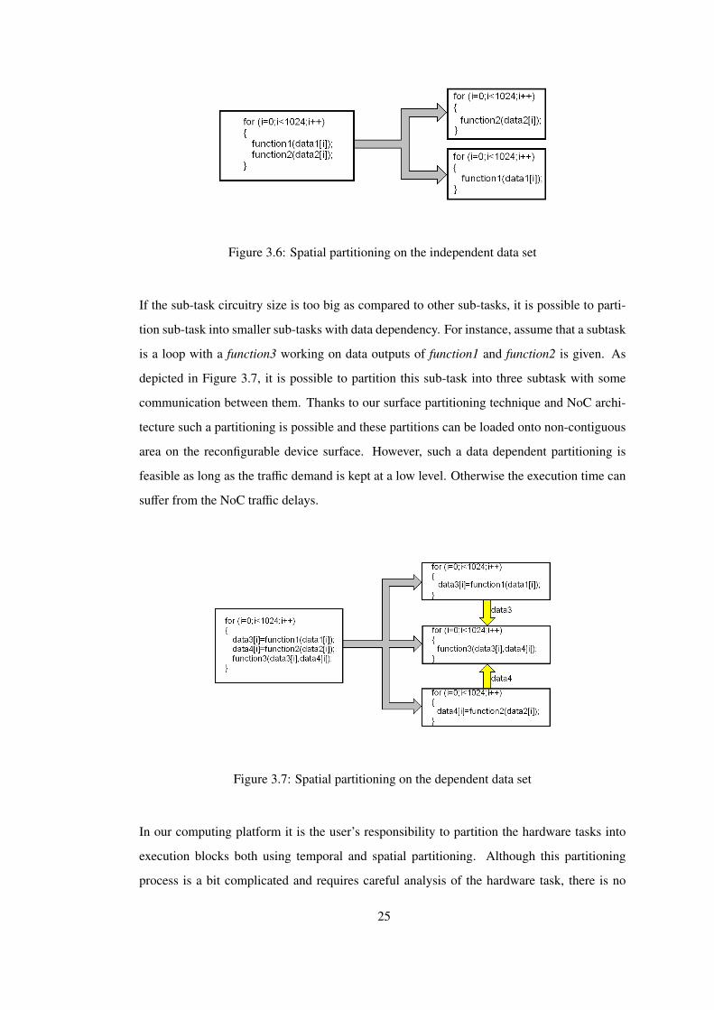
Figure 3.6: Spatial partitioning on the independent data set
If the sub-task circuitry size is too big as compared to other sub-tasks, it is possible to parti-
tion sub-task into smaller sub-tasks with data dependency. For instance, assume that a subtask
is a loop with a function3 working on data outputs of function1 and function2 is given. As
depicted in Figure 3.7, it is possible to partition this sub-task into three subtask with some
communication between them. Thanks to our surface partitioning technique and NoC archi-
tecture such a partitioning is possible and these partitions can be loaded onto non-contiguous
area on the reconfigurable device surface. However, such a data dependent partitioning is
feasible as long as the traffic demand is kept at a low level. Otherwise the execution time can
suffer from the NoC traffic delays.
Figure 3.7: Spatial partitioning on the dependent data set
In our computing platform it is the user’s responsibility to partition the hardware tasks into
execution blocks both using temporal and spatial partitioning. Although this partitioning
process is a bit complicated and requires careful analysis of the hardware task, there is no
25

restriction on the number of the execution blocks and the execution blocks circuitry can be in
any size.
As compared to existing work [19-21], which requires partitioning into fixed sized circuits, we
provide a design flexibility to users. Indeed in previous methods, it is the user’s responsibility
to select a ‘good number’ for this fixed sub-circuit size, which makes partitioning compli-
cated. Since it is almost impossible to have sub-tasks all having the same size, restricting
circuit size to a fixed value will definitely result in fragmentation. Similarly, in multi-tasking
systems as the characteristics of tasks are different, the fixed size selection process becomes
more problematic.
Our aim is to provide design flexibility similar to the one provided by conventional program-
ming to application programmers. Therefore, in our proposal application programmer is free
to choose the size of each execution block. In addition to this flexibility, we aim to achieve
much better device utilization compared to fixed size partitioning.
In this study, we model a hardware task with a 3-tuple as HT (S EB,G,D) where;
• S EB is the set of execution blocks
• G is a directed graph representing the parallelism and dependencies between execution
blocks
• D is the deadline of the task to be completed for hard real time tasks.
Also, a level k in the dependency graph G is mathematically modeled as Lk(G) and it represent
the execution blocks that are obtained by spatial partitioning and operating in parallel.
An example hardware task flow is given in Figure 3.8. The execution of hardware task starts
with EB0 followed by EB1, after which three other execution blocks EB2, EB3, EB4 will
start execution in parallel. Just after the completion of both EB3 and EB4, EB6 will start
execution in parallel with EB5. Finally the hardware task execution will be completed with
EB7 that will be executed after the completion of EB5 and EB6.
26

Figure 3.8: An example hardware task dependency graph
The improvements that are achieved with our hardware task model compared to existing
works are discussed below:
Reconfiguration time & task turnaround time Most of the existing works require configu-
ration of all hardware task bit-streams for task switching, however our solution allows a
hardware task to start execution just after the first execution block bit-stream is config-
ured on the reconfigurable hardware since the following blocks can now be configured
in a pipeline manner. In other words, we minimize the reconfiguration time penalty and
achieve a shorter task turnaround time. Assuming that both execution and configura-
tion times are equal and assuming one time unit for all the hardware execution blocks
in Figure 3.8, task turnaround time will reduce from 13 to 9 time units.
27

Task preemption & rescheduling With our execution block based hardware task model, it
is possible to stop execution of the task at execution block boundaries, i.e. task can be
preempted as soon as the currently executing execution block completes its operation.
In this way we can achieve ‘a soft priority scheduling’ with no big time penalty for
storing the task context.
Reconfigurable Hardware Utilization & Device Size In our computing model, it is possi-
ble to schedule a task with a size larger than the reconfigurable hardware size and
decrease the device cost. Indeed the effective hardware task area is shrunk by reusing
the area that was previously allocated to a completed execution block and therefore the
device utilization is increased. The wasted area due to fragmentation issues is also kept
at minimum by packing more than one execution block into a fixed size reconfigurable
hardware area as will be illustrated in the following sections.
3.4 Execution Block Model
In our computing model, after partitioning a hardware task into a set of execution blocks, it
is the application developer’s responsibility to define these execution blocks in a hardware
description language (HDL). The rest is handled by our reconfigurable computing platform.
Our novel offline bit-stream generation process and hardware operating system will then be
responsible to execute the hardware task in the most efficient way.
In order to be compatible with our reconfigurable computing platform, each execution block
must have input/output interfaces as depicted in Figure 3.9.
In an execution block, the computation starts with a trigger signal on Start port. The input
data for computation is received from system memory over SAC In. If the execution block is
obtained by data dependent spatial partitioning, the data can be received from another execu-
tion block belonging to the same hardware task over Data In port also. In a similar way, the
computational results can be stored back to system memory over SAC Out or sent over Data
Out port to another execution block belonging to the same hardware task. Indeed, the SAC
In and SAC Out ports are used for operating system services like inter-task communication.
Note that if the execution block is not obtained by data dependent spatial partition, then there
is no need for Data Out and Data In ports.
28

Figure 3.9: An interface template for an execution block
In this thesis, we model an execution block with a 5-tuple as EB(B,C,TMWrite ,TMRead ,TOUT ),
where
• B is number of logic resources needed to implement the execution block
• C is the execution time for the execution block on the target reconfigurable hardware.
• TMWrite is the memory write demand in MByte/s
• TMRead is the memory read demand in MByte/s
• TOUT is the data generation rate at the Data Out port in MByte/s
3.5 Surface Partitioning Model
Reconfigurable hardware surface partitioning technique plays a key role in the overall system
performance. It directly affects the underlying reconfigurable hardware utilization and hence
has great impact on the required reconfigurable device size, cost and power consumption.
Our extensive literature survey and discussion on surface partitioning given in Chapter 2 has
shown that, none of the existing surface partitioning methods is directly applicable to our
reconfigurable computing platform.
Due to its support for communication media and no time consuming packing or defragmenta-
tion requirements, fixed block size partitioning is chosen. Among the fixed block partitioning
alternatives, the 1D partitioning suffers from shared and limited bandwidth communication
29

media and low operating frequency within partitions due to long wires. Therefore 2D fixed
sized surface partitioning technique is our choice. Existing surface partitioning techniques
(for example [20-21]) neither model the communication media nor describe how to select
the 2D partitioning parameters. Therefore a novel surface partitioning model specific to our
reconfigurable computing platform is developed.
In our partitioning model, we first allocate some fixed sized rectangle regions in a 2D grid
manner as shown in Figure 3.10. These rectangle regions are called ‘user block’ and they are
dynamically reconfigured for hardware task implementation. The rest of the reconfigurable
device surface is allocated for communication media and hardware operating system. This
area is static and the associated bitstream is loaded at system startup.
Figure 3.10: 3x3 user block allocation
The static area, which is called as ‘System Area Circuitry (SAC)’ in the rest of document,
is composed of three function circuitry. First circuitry is used to implement the platform
specific ‘host&memory interface’. The second circuitry is the circuitry for the hardware op-
erating system. The third circuitry is the communication media for communication between
user blocks and host&memory interface. In our surface partitioning technique, we reserve the
outer area for host&memory interface and the hardware operating system implementations.
The remaining static area is used for the communication media and is called inter block com-
munication network (IBCN) in the rest of this document. Our surface partitioning technique
is summarized for a 3x3 user block partitioning in Figure 3.11.
Thanks to our IBCN architecture, the reconfigurable computing platform is not restricted to
30

Figure 3.11: Proposed surface partitioning model for 3x3 user block
use a single reconfigurable device. The IBCN provides seamless communication media for
user blocks to access other user blocks and host&memory interface. Therefore, it is possible
to use more than one reconfigurable device with connection over IBCN. With this approach,
as shown in Figure 3.12, it is also possible to merge a number of reconfigurable hardware into
a single virtual reconfigurable hardware. Such a reconfigurable hardware will be treated as
a single reconfigurable device both by the application programmer and hardware operating
system.
Figure 3.12: Merging example: Four reconfigurable devices merged into a virtual reconfig-urable device
31

3.6 Placement Model
Since we use a fixed block size based partitioning, no external fragmentation problem exists
while internal fragmentation is not a big issue due to our novel hardware task model and
offline bitstream generation process where the execution blocks of a hardware task can be
packed into a number of user blocks. In contrast to existing models [20,21,26], where block
size is chosen as equal to the size of the largest hardware task circuitry, we allow hardware
tasks to be configured onto more than one user blocks that are not necessarily contiguous.
In our placement model any free user block can be allocated to the task. If there is data
connectivity between any two execution blocks, IBCN provides the necessary communication
path between these if they are mapped into different user blocks. In order to minimize the
affects of the IBCN on execution time, an ad-hoc mapping technique is presented, which will
be discussed later in Chapter 6. An example placement for a set of four tasks is shown in
Figure 3.13.
Figure 3.13: A placement example: surface partitioning for a set of four tasks
3.7 Reduced Hardware Task Model
In our reconfigurable computing platform, a hardware task is defined in terms of a set of
execution blocks, a dependency graph and a deadline. The user is free to have different size
execution blocks. With the help of our offline packing process, we will convert a hardware
task into a set of equal sized user blocks and call the resulting circuit as ‘reduced hardware
32

task’.
For a given hardware task HT , we model the reduced hardware task with the 3-tuple as
HT ′(S UB,G′,D) where,
• S UB is a set of user blocks
• G′ is a directed graph representing the parallelism and data dependencies between user
blocks
• D is the deadline for its completion of execution.
An example hardware task and its corresponding reduced hardware task (b) are shown in
Figure 3.14. Note that in this example, the reduced hardware task is obtained by packing
execution blocks into user blocks with size of 40K logic blocks.
Figure 3.14: a) An example hardware task b) its reduced hardware task
33

3.8 Context Loading Model
As was stated earlier, our reconfigurable computing platform aims to provide short turn
around time for scheduled hardware tasks. The task turn around time is composed of ex-
ecution time and reconfiguration time. In this thesis work, we used the following context
loading scheme to minimize the task turn around time whenever a hardware task is scheduled
by the user:
Step-1 (Initialization) Starting from the one with the largest execution time, load all user
blocks (UBs) in the first level of reduced task dependency graph L1(G′). Whenever a
user block is loaded, it immediately starts execution in this initialization step.
Step-2 Just after all user blocks are loaded for the first level, continue loading the ones in the
second level L2(G′) and set k = 1.
Step-3 Wait till all user blocks on Lk(G′) complete their execution. Set k = k + 1.
Step-4 If all user blocks on Lk(G′) are already loaded, start user blocks on Lk(G′) and go to
Step-6.
Step-5 Wait till all user blocks on Lk(G′) are loaded and start user blocks on Lk(G′) (prefetch-
ing).
Step-6 Start loading user blocks in level Lk+1(G′).
Step-7 Go to Step-3 if end of G′ is not reached.
Using the above context loading scheme, the execution time can be locally minimized by
executing user blocks that have no data dependency in parallel. The reconfiguration time is
minimized by prefetching the next level user blocks while current level user blocks are being
executed.
34

CHAPTER 4
USER BLOCK SIZE SELECTION
In our hardware task model, the execution blocks are application dependent and can be in
different sizes. Since we pack execution blocks of a task into a number of fixed size user
blocks, it is possible to have some empty spaces in the user block. This empty space can be
considered as internal fragmentation and it can decrease the overall reconfigurable hardware
utilization if the user block size is not properly selected. Similarly, the IBCN circuitry is im-
plemented with the resources of the reconfigurable hardware and the area reserved for IBCN
should be kept optimal for a high level of device utilization while providing the necessary
communication paths. Since the area needed for IBCN is directly proportional to the number
of user block, the surface partitioning should be done carefully in order not to waste too much
space for IBCN implementation.
In this dissertation, we address embedded applications for which it is possible to find an
optimal user block size because we have the knowledge of all hardware tasks and execution
blocks prior to field operation. For better device utilization, we introduce the following offline
optimization process to find the 2D block partitioning parameters.
Part of the reconfigurable hardware surface is used for static SAC, which is composed of
host&memory interface and hardware operating system circuits. In the rest of the thesis, we
model the SAC with the ordered pair as S AC(MS AC ,NS AC) where;
• MS AC is the number of outer vertical logic blocks used for SAC.
• NS AC is the number of outer horizontal logic blocks used for SAC.
The implementations of the host&memory interface and hardware operating system are plat-
35

form dependent and not affected by the user block size selection. Therefore MS AC and NS AC
values are considered as constant for the user block size selection process.
Similar to SAC implementation, the IBCN implementation requires some surface area on the
reconfigurable hardware. But the size of this area depends on the user block size. When the
reconfigurable hardware is partitioned into m × n user blocks, we model the communication
path with the four-tuple as IBCN(m, n,MIBCN(m,n),NIBCN(m,n)) where;
• m is the number of user blocks in horizontal axis.
• n is the number of user blocks in vertical axis.
• MIBCN(m,n) is the number of total logic blocks needed for IBCN in horizontal axis.
• NIBCN(m,n) is the number of total logic blocks needed for IBCN in vertical axis.
Using the above circuit models, the user block size (UBS) then becomes;
UBS =
{(M−MS AC−MIBCN(m,n)
)m
}×
{(N−NS AC−NIBCN(m,n)
)n
}
In our surface partitioning technique, the selection of partitioning parameters is important in
determining the efficiency of device usage. In Figure 4.1a, a reconfigurable device with a size
of M×N logic blocks and in Figure 4.1b a hardware tasks containing a set of execution blocks
are given. Note that, the given execution blocks are composed of a number of logic blocks
(Figure 4.1b). After allocating outer NS AC logic blocks in horizontal axis and MS AC logic
blocks in vertical axis for SAC implementation, the remaining parts are partitioned into m× n
user blocks and a predefined area is reserved for IBCN switch implementation for each user
block (Figure 4.1c). With the completion of the partitioning process, for each hardware task,
the execution blocks are packed into user blocks. In order to achieve higher device utilization,
the partitioning parameters m and n must be chosen in such a way that the following figures
of merits are both maximized.
• utilization of the user area ρuser, which is the ratio of ‘gray area’ to ‘all minus SAC
area’ (Figure 4.1c).
36

• utilization of the area within user blocks ρinternal, which is the ratio of area filled by
execution blocks to user block size after the execution block packing process (Figure
4.1d).
Figure 4.1: Problem of user block size selection
4.1 Problem Formulation
Given;
• a reconfigurable hardware, RHW(M,N,T ) where
– M is the number of logic blocks in a row.
– N is the number of logic blocks in a column.
– T is the reconfiguration time needed for a single logic block.
• an SAC implementation, S AC(MS AC ,NS AC) where
– MS AC is the number of outer vertical logic blocks used for SAC.
– NS AC is the number of outer horizontal logic blocks used for SAC.
• a set Y of hardware tasks where
– a hardware task j is modeled as HT j(S EB j ,G j,D j) including the set of execution
blocks S EB j , dependency graph G j and a deadline D j
37

– an execution block i in HT j is modeled as EBi, j(Bi, j,Ci, j), where Bi, j is the number
of logic resources needed to implement the execution block i of hardware task j
and Ci, j is the execution time for the execution block i of hardware task j on the
specific reconfigurable hardware.
– a level k in the task dependency graph G j is modeled as Lk(G j) and it represent
the execution blocks that can be executed in parallel in hardware task j.
• user provided device utilization factor β j for each hardware task j. β j value should be
selected within the range [0, 1] and for a task that will be executed only once, β j should
be small, but for periodic tasks it should be large. Choosing an improper β j value may
result in degraded reconfigurable hardware utilization.
Problem P is to find m and n, i.e. the number of user blocks in horizontal and vertical di-
mensions respectively such that when the reconfigurable hardware is divided into m × n user
blocks, total reconfigurable hardware utilization, ρtotal, is maximized. Hence;
Problem P: max{ρtotal}
subject to
∀ j ∈ Y,∀i ∈ S EB j : M × N ≥ UBS ≥ max(Bi, j) (4.1)
∀ j ∈ Y,∀k ∈ G j : e f f ective_size(HT j) ≥ max( ∑
i∈Lk(G j)
Bi, j +∑
i∈Lk+1(G j)
Bi, j
)(4.2)
where
• ρtotal = ρuser × ρinternal
• ρuser = m×n×UBS(M−MS AC)×(N−NS AC) which represents the ratio of area usable by user
hardware tasks to total available area
• ρinternal =
∑j∈Y (ρinternal j×β j)∑
j∈Y β jwhich represents the average internal utilization
• ρinternal j =size_o f (HT j)
e f f ective_size(HT j)which represents the internal utilization for hardware
task j
38

• size_o f (HT j) =∑
i∈S EB jBi, j which represents the sum of logic requirements for
execution blocks within the set S EB j for hardware task j
• e f f ective_size(HT j) = r j × UBS which represents the maximum logic resources
needed for hardware task j during its execution
• r j is the maximum number of user blocks allocated to hardware task j by the scheduling
mechanism at any instance
• UBS =
{(M−MS AC−MIBCN(m,n)
)m
}×
{(N−NS AC−NIBCN(m,n)
)n
}• m, n ∈ {1, 2, 3, ...}
Note that the computation of the e f f ective_size(HT j) and hence r j of a hardware task j
depends on the hardware task dependency graph G j and user block size UBS and therefore
requires another optimization problem.
Finding e f f ective_size(HT j) can be modeled as a subproblem P1 as follows:
Given
• a hardware task HT j with a set of execution blocks S EB j and dependency graph G j
• the user block size UBS
Problem P1: min{r j}
subject to
∀ j ∈ Y, ∀k ∈ G′j : r j = max{noubk + noubk+1} (4.3)
∀ j ∈ Y, ∀i ∈ S EB j : 1 =∑
k∈S UB j
xi,k (4.4)
∀ j ∈ Y, ∀i ∈ S EB j , f orallk ∈ S UB j : xi, j ∈ {0, 1} (4.5)
∀ j ∈ Y, ∀k ∈ S UB j : UBS ≥∑
i∈S EB j
xi,k × Bi, j (4.6)
39

∀ j ∈ Y, r j ∈ {1, 2, 3, ...} (4.7)
where
• noubk is the number of user blocks at level k of G′j;
• xi,k is a binary variable defined as follows:
xi,k =
1 if EBi is packed in UBk
0 otherwise
In the above optimization problem constraint (4.1) indicates that the user block size UBS must
be at least the size of the largest execution block in the system. This is because the execution
blocks are atomic and the whole circuitry for one execution block must be loaded onto the
same user block. Constraint (4.2) appears in our formulation due to our heuristic approach on
context loading process (see Section 3.8) that is used to minimize the task turn around time.
This constraint guarantees for each hardware task j that at least an area equal to the maximum,
taken over all levels, of the sum of execution block sizes in two consecutive levels of the
dependency graph G j is allocated for execution without any time penalty for reconfiguration.
In a similar way, constraint (4.3) indicates that the number of user blocks needed for a task j
should be equal to the sum of the number of user blocks in two consecutive levels of reduced
hardware task graph G′j. Constraints (4.4) and (4.5) guarantees that an execution block is
atomic and can be packed into one user block only. Finally, the sum of logic requirements of
execution blocks packed into the same user block cannot be larger than UBS (constraint 4.6).
4.2 Problem Analysis
For the optimization problem P, the quality of the solution strongly depends on the ρinternal
value calculated for a given UBS . Because for the given hardware tasks and UBS maximizing
ρinternal is an objective of our second optimization problem P1. In our proposal, instead of
loading just a single execution block to a user block on the reconfigurable harware surface,
we propose to pack execution blocks working in parallel into user blocks. In this way the r j
value, hence e f f ective_size(HT j), can be minimized.
40

Since the execution blocks are atomic and it is not feasible to partition them further into
smaller units, we have to pack these different sized execution blocks into fixed sized user
blocks having size of UBS . This packing process is known as ‘one dimensional bin-packing
problem (BPP-1)’ in the literature. Coffman et al. have shown that one dimensional bin-
packing problem is NP-complete [44]. Since part of optimization process P1 is NP-complete,
then our optimization problem P is NP-complete too.
For a given UBS and hardware task j, calculation of ρinternal requires the solution of BPP-1
for all execution blocks on the same level in G j. The BPP-1 is a well studied topic in the
literature and some major works are discussed below.
4.3 Literature survey on BPP-1
Since BPP-1 is NP-Complete, mostly heuristics techniques were proposed to find near optimal
solutions. Jatinder et al. [45] introduced a heuristic based on minimum bin slack (MBS) and
it has been shown that this method finds optimal solutions if the sum requirements of items is
less than or equal to twice the bin capacity.
In [46] an exact solution procedure for BPP-1 was proposed. This technique, called BISON, is
composed of different bound arguments and reduction procedures, several heuristics including
tabu search and a branch and bound procedure. It is shown that BISON finds exact solution
for most of the time.
Flezsar and Hindi [47] have proposed several heuristic methods also. Some of the proposed
heuristics are based on MBS and the variable search results. Computational results have
shown that the most effective algorithm was the one using the MBS to generate initial so-
lutions and using variable neighborhood search (VNS) method to find exact solutions based
on generated initial solution. The authors reported that this technique found optimal solu-
tions for 1329 instances and finds 4 better solutions than best known out of 1370 well known
benchmark.
A hybrid heuristic called HI-BP was proposed by Alvim et al. [48]. In this method a combi-
nation of lower bounding strategies, the generation of initial solutions by the dual min-max
problem, the use of load redistribution based on dominance, differencing, and unbalancing;
41

and the inclusion of an improvement process utilizing tabu search methods were combined
to achieve better results. Computational results have shown that the proposed hybrid method
generates better results compared to BISON and VNS method.
In 2006, a weight annealing based heuristics was proposed by Loh [49]. Starting from an
initial solution obtained with first-fit decreasing methods, weights are assigned to distort sizes
according to the packing solutions of individual bins. Then a local search was carried out to
swap the items. Iteratively this weighting and local search procedure was carried out with a
cooling schedule. The proposed technique was applied to both BBP-1 and BBP-2 problems
and it has been reported that with its O(n3) complexity, this technique gives the best result
among existing methods.
In our computing platform, the bin packing decision is given during our offline bitstream
generation process. Therefore instead of designing a new BBP-1 solver, we selected the
existing weight annealing based heuristics [49] as our BBP-1 solver and used it for the solution
of subproblem P1 in our model.
4.4 Greedy Heuristic for User Block Size Selection
Since optimization problem P is NP-complete, we seek a sub-optimal solution in bounded
time. Our greedy method starts with an initial solution, where UBS is equal to the whole
reconfigurable device size. With such a UBS , ρuser will be maximized but ρinternal will have
the worst value. We then decrease UBS by increasing m and then n values at each iteration
such that the user block will be in a square like shape. This iterative process decreases ρuser,
increases ρinternal and continues till there is no improvement in ρtotal.
The proposed heuristic finds a good but non-optimal solution for m and n values when it
terminates. Another termination criterion is that UBS should at least be equal to the size
of the largest execution block, EBmax, in the given hardware tasks list. Calculation of ρuser
requires finding effective circuit size and hence bin packing of execution blocks at the same
level of the dependency graph into user blocks. The pseudo code of our greedy heuristic
proposal and the pseudo code for finding effective circuit size are given in Figure 4.2 and
Figure 4.3 respectively.
42

Figure 4.2: Pseudo code for greedy heuristic user block size selection
43

Figure 4.3: Pseudo code for finding effective circuit size
4.5 Quality Analysis for Greedy Heuristic
As was stated earlier, the NP-completeness of our optimization problem P is due to having
BPP-1 as its sub-problem. In order to show how well our greedy heuristic is, a comparison
using a relaxed upper bound has been performed. The relaxed upper bound is obtained by
removing constraint (4.4) that guarantees the execution blocks are to be atomic. In this new
relaxed sub-problem, there is no need to solve BPP-1 and the number of user blocks needed
to pack execution blocks at level k in G becomes simply;
ceil⌈∑
i∈Lk(G j) Bi, j
US B
⌉With this relaxation the complexity of Prelaxed becomes O(n3). The exact solution of Prelaxed
now provides an infeasible solution and an upper bound for the optimal and can therefore be
used to judge the quality of our heuristic solution.
In order to find the average gap between solutions provided by our proposed greedy heuris-
tic and Prelaxed solution, a simulation study has been carried out. In these simulations, 100
test cases are created by randomly generating 1000 hardware tasks for each case and the
44

number of execution blocks are selected between 100 and 200 randomly. Similarly, the ex-
ecution block sizes are randomly selected in the interval [10K − 40K] logic blocks and the
dependency graph depth is randomly selected between 3 and 10. The device under study is
assumed to be 5 million logic block equivalent and the area wasted for IBCN is modeled as
8K × number of user blocks.The simulation result has shown that the gap between our greedy
heuristic and the relaxed upper bound for ρtotal value is around 4.5% with a confidence interval
of 97%.
45

CHAPTER 5
INTER BLOCK COMMUNICATION NETWORK
ARCHITECTURE
In the proposed reconfigurable hardware surface partitioning methodology, the area between
the user blocks are dedicated for inter block communication network (IBCN). Since our ex-
ecution packing process can pack execution blocks that operates in parallel but have data
decency into different user blocks, IBCN is then responsible for providing this data path. In
a similar manner, the memory access demands of user blocks are handled by IBCN. Finally,
IBCN is also the communication media for high level operating system services and inter-task
communication between hardware tasks and software task. In this thesis work, a novel Net-
work on Chip (NoC) architecture is designed to provide the necessary support as IBCN. In this
chapter, first the communication requirements on our IBCN are analyzed. Then an extensive
literature survey is given for existing NoC architectures. Finally, the proposed architecture is
presented in detail with all its building blocks.
5.1 Communication Requirements
In our reconfigurable hardware platform, IBCN is responsible to provide communication and
data path between;
• user blocks of a hardware task (for handling data dependency)
• user blocks belonging to different hardware tasks (for inter-task communication)
• user blocks and host processor (for inter-task communication between software task
and hardware tasks)
46

• user blocks and host processor (for high level operating system service)
• user blocks and external memory (for memory read and write access)
• user blocks and hardware operating system (for task management and high level oper-
ating system services).
Below, these communication requirements are analyzed in detail.
5.1.1 Task Level Communication Requirements
In the proposed reconfigurable computing platform, it is required to partition a hardware task
into a set of execution blocks. This partitioning process aims improving device utilization and
reconfiguration time overhead. In this way, it is possible to synthesize, place and route the
execution blocks individually in a much more efficient way as compared to whole hardware
task. Also, the operating frequency of execution blocks will be much faster than the whole
hardware task due to possible long wire delays in reconfigurable devices. Finally, it may now
be possible to obtain optimized library for execution blocks in a much shorter design time.
Despite these advantages, some new communication requirements arise when a whole hard-
ware task is partitioned into execution blocks. If the execution blocks having data dependen-
cies are packed into different user blocks, then the DATA PATH traffic demand arises between
user blocks. The other traffic requirement is the control signals between hardware operat-
ing system and the user blocks. A TRIG SIGNAL must be sent from the hardware operating
system when it is time to start the execution of a user block according to reduced hardware
task dependency graph. In a similar fashion, a FINISH SIGNAL must be sent to hardware
operating system by the user block completing its execution.
5.1.2 Memory Access Requirements
Unified memory architecture is used in our reconfigurable computing platform. Although it
is possible to implement this memory on the reconfigurable hardware, it will consume too
much logic blocks and will operate at slower frequency than commercially available memory
devices. Indeed, this memory should be accessible by the GPP also. Therefore, although it
is not mandatory, an external memory is assumed for IBCN discussion. However, it is still
47

possible to implement a small sized low latency access register file for each execution block
depending on its local memory requirement.
In our model, execution blocks can perform memory read and memory write individually.
Therefore, there will be more than one memory access requirement at the same time. In
the proposed IBCN architecture, these memory access requirements are routed to system
area circuitry, which is responsible for physical memory access. The memory writes will
be a posted message with data, i.e. execution block will not wait till the data is written into
memory and it requires M_WRITE message to be sent from the execution block to system area
circuitry. The memory read will be a REQUEST message from execution block to system area
circuitry and later followed by an M_READ message with data from the system area circuitry.
5.1.3 Operating System Services Communication Requirements
In a multi-tasking computing system, there is a need for data exchange and synchronization
between tasks, i.e., there is a need for inter-task communication. In general such a commu-
nication between tasks are handled using operating system services like semaphores, pipes,
sockets and mailboxes. All of these inter-task communication methods require system calls
to operating system kernel. In a similar fashion, high level operating system services like file
system and networking requires system calls.
In our reconfigurable computing platform these communication demands for software task is
handled by the commercial operating system. In case of a communication request between
a software task and hardware task; the commercial operating system and both parts of our
hardware operating system are working together. The communication of the hardware task
starts with the SYS_CALL message from hardware task to the hardware operating system
circuitry on the reconfigurable hardware. This message is forwarded to the software part of
the hardware operating system over host interface and necessary action is performed there.
For a communication request from the software task, the reverse path is fallowed and the
hardware operating system circuitry sends TASK_CALL message to the target user block.
The communication demand between two hardware tasks is handled in a similar fashion.
SYS_CALL messages are sent to hardware operating system circuitry and responses are re-
ceived via TASK_CALL messages. Although it is possible to have a peer to peer communica-
48

tion between two hardware tasks over IBCN, the communication demand between hardware
tasks is also handled over our hardware operating system circuitry. Because, in some cases the
target hardware task can be waiting in the queue for context loading or the execution of target
hardware task does not reach yet to a point to handle this communication. Indeed, for peer
to peer communication a register needed in the hardware tasks to keep the physical location
of the receiver hardware task. This requires extra hardware area and should be updated if the
receiver hardware task is scheduled later than the sender hardware task.
The above discussion on the communication requirements are summarized in Table 5.1.
Table 5.1: IBCN message types and their characteristics
Name Source Destination Size Priority FrequencySTART SIGNAL SAC User Block Short High LowFINISH SIGNAL User Block SAC Short High LowDATA PATH User Block User Block Long High ModerateSYS_CALL User Block SAC Short Low LowTASK_CALL SAC User Block Short Low LowREQUEST User Block SAC Short High HighM_WRITE User Block SAC Long High HighM_READ SAC User Block Long High High
5.2 Literature Survey on NoC
The 2D fixed block base reconfigurable hardware surface partitioning technique with the idea
of using the area between blocks for communication media has been discussed in a number of
studies [20, 21, 26]. However, these studies were lack of information about the architecture
and implementation of this communication media. On the other hand, our IBCN functionality
is very similar to ‘network on chip (NoC)’ functionality in ‘system on chip (SoC)’ architec-
tures. The NoC is a well studied subject in literature and below, some major works targeting
2D mesh topologies are discussed briefly.
With the advances in silicon process technology, it becomes cheaper to build SoC devices
with a number of processor cores, storage units and external peripheral interfaces. Since
the time-to-market is a critical issue, proven intellectual property (IP) cores are used in SoC
design. However, IP’s come with its own connectivity interface and have different clock
49

frequency demands. In addition, with deep-submicron processes the long wires became a
limiting factor for high speed operation. As a remedy, the NoC architecture was used for
connectivity between IP cores instead of shared bus architecture with fixed frequency. The
NoC architectures are packet switching networks with different routing and packet structures.
One of the earliest NoC architecture was a 2D folded torus NoC architecture [50]. For a 4× 4
tile based SoC with processors and DSPs, the physical design and bandwidth problems of
the shared bus architecture were solved with just 6.6% silicon area overhead for interconnect
network. In the proposed network, a 5-port router was used with pre-scheduled virtual channel
for static traffic and cyclic reservation for dynamic traffic.
In literature lots of research has been carried out on NoC implementation for specific SoC
architectures. For NoC implementation targeting general purpose applications, with its dead-
lock free nature and its low logic requirement, it has been observed that wormhole switching
technique was the preferred choice as compared to store and forward and virtual cut-through
switching [51]. A low area implementation of wormhole switching was given in [52] for 2D
mesh topology and very promising results were reported both in terms of area requirement,
bandwidth and latency.
In addition to SoC design, the NoC concept was studied for reconfigurable architectures also.
In [53], Majer et al. presented a dynamically changing network architecture, called DyNoC,
for run time partially reconfigurable architectures. In DyNoc, similar to our model, the recon-
figurable device is partitioned into 2D small sized grids and area between the grids is used for
NoC implementation. The user applications were placed onto this fine grained grid, where
the allocated region must be in rectangle shape. When an application was placed, the recon-
figurable device resources allocated for NoC on the placed region were also used for user
application. Therefore a dynamic network architecture was proposed to cope with changing
network topology and three different routing techniques were discussed.
Another dynamic network architecture for run time reconfigurable architecture was studied in
[54]. The proposal was to place a network switch while placing a user application on to device.
The placed switch was connected to the rest of the network by using the nearest available
switch by reconfiguring necessary wires between two switches. Routing decisions are kept
on a dynamic table which was updated when placement or removal of a user application takes
place. Whenever an application completes its operation, the associated switch was removed
50

from the reconfigurable device surface also.
Corbetta et al. [55] has proposed a communication infrastructure for reconfigurable system
implementation. This infrastructure aimed to reduce the design complexity of communication
cores and provide fault tolerant communication support. In spite of these advantages, large
resource requirement and long reconfiguration times were reported.
In 2009, a dynamic scalable communication structure for dynamically reconfigurable FP-
GAs was proposed in [56]. With the aim of providing communication between dynamically
placed modules the proposed method, called as CuNoC, routes the addressed data packets
from source to its destination over a dynamically changing connectivity. Similar to DyNoc,
the surface was first partitioned into processing elements and communication unit. A number
of processing element and communication unit resources were used for task implementation
and it was required that each task has at least one communication unit. With similar commu-
nication bandwidth, the authors reported very low logic requirement for the network port as
compared to DyNoc.
To the best our knowledge, none of the existing NoC implementations is suitable to be di-
rectly used in our computing platform. Although dynamic behaviors are handled in some of
the discussed studies, the communication requirements of our platform are completely differ-
ent than the reported ones. None of the above implementation gives a solution for external
memory communication or intra-task data path communication. A dynamically changing net-
work requires too much time adopt itself to changing reconfigurable hardware usage. Since
we expect very frequent changes in reconfigurable hardware surface usage, such a network
will also not be useful for our computing platform.
5.3 Inter Block Communication Network Architecture
The simplest way to implement the IBCN is to use a shared bus architecture as given in
[19,17]. However, due to limited bandwidth and implementation difficulty in our 2D recon-
figurable hardware surface partitioning, we prefer to employ a switching NoC architecture
similar to SoC architectures. The proposed NoC implementation is specifically designed and
developed for our reconfigurable platform to meet the traffic demand discussed above in Sec-
tion 5.1. The architectural details of our NoC implementation for IBCN is given below.
51

5.3.1 IBCN Topology
The NoC topology is a key factor for the IBCN implementation. Since part of the reconfig-
urable hardware is allocated for IBCN implementation, the IBCN topology must be chosen in
a such a way to minimize the logic block requirement and to provide a high throughput while
being scalable with the number of user blocks. In literature a number of NoC topologies were
discussed for 2D grid based placement of IPs.
In the Octagon topology [57], every node in the eight node network was connected to three
other nodes such that any two nodes in the network are at most two hops away. It was possible
to expand the network by connecting more octagon topologies with each other. With such a
connectivity, it was possible to provide high bandwidth with low latency for random source
destination pair. Despite these advantages, the Octagon topology requires too much area
for its implementation. Indeed, this area requirement grows exponentially with increasing
number of nodes.
Pande et al. [58] has proposed a butterfly fat tree NoC topology, where four IP blocks are
located in leaves connected to switches and a switch was connected to two parent switches.
In this manner a scalable NoC topology was achieved with very low communication latency
between nodes having the same parent node. When traffic generation becomes random, as the
order of parent nodes increases, i.e. the subnet size grows, latency increases. In order to get
rid of this limitation, a fat-tree network topology, called SPIN, having two stage parent switch
was used [59]. In SPIN topology, a switch was connected to four parent switches to minimize
the hop distance and to provide alternative paths. Although, low latency and high bandwidth
was achieved, SPIN topology suffers from large area requirement.
Since our placement strategy can place the context of two user blocks having data path be-
tween them onto any free location on the reconfigurable hardware surface, the traffic demand
in our computing platform can also be modeled as random. Therefore, we preferred to use 2D
mesh architecture because of its simplicity, less logic resource requirement and suitability for
our partitioning in terms of placement, routing and scalability.
Our proposed IBCN topology is based on a 5-way switch, where one port of the switch is
connected to the user block and the remaining four ports are connected to 5-way neighboring
switches in north, west, south and east directions. Although there is a single SAC, which
52

is responsible for host and memory access, we introduce multiple access points (APs) at
IBCN and SAC junctions. With the existence of these multiple IBCN APs, the traffic demand
towards host and memory is routed to the nearest AP resulting in better IBCN throughput and
latency compared to having a single access point to SAC. The APs communicate with the
SAC in a round robin fashion for fair access to external memory and reconfigurable hardware
operating system circuitry. Figure 5.1 illustrates the proposed IBCN topology for 3x3 surface
partitioning.
Figure 5.1: IBCN topology for 3x3 surface partitioning
5.3.2 IBCN Switching and Flow Control
In the literature both circuit and packet switching techniques are employed in NoC archi-
tectures. In our case however, circuit switching technique is not applicable to IBCN due to
53

random traffic demand and short packet sizes. Therefore, a packet switching technique is
employed in the proposed IBCN architecture.
Store&forward, virtual cut-through and wormhole techniques are among the existing packet
switching methods. All of these require buffers at the switches for temporary storage of the
network packets. In store&forward mode, a switch waits until a packet is completely received
and after reception of the packet contents are examined to decide what to do, which implies
per-switch latency. Therefore its overall latency is directly related to both packet size and hop
distance between communicating pairs. On the other hand, in virtual cut-through mode, a
switch can forward a packet as soon as the next switch gives a guarantee that a packet will be
accepted completely without waiting to receive the whole packet. But, it is still necessary to
have a buffer to store a complete packet, like in store&forward mode, but with lower latency
communication in this case.
Both store&forward and virtual cut-through modes require large buffer space especially for
large packet sizes. In order to decrease this buffer space requirement, a variant of virtual cut-
through mode called wormhole switching [51] is used. In this mode, a packet is composed of
fixed size units called flits (flow control digits-the smallest unit of flow control). The header
flit reserves a path from source-to-destination while it is routed. Rest of the flits follow this
path in a pipelined manner. Finally, the tail flit removes the reservation on the path.
Due to its low buffer space requirement and low latency, we prefer to use wormhole switch-
ing mode. Despite these advantages, this method causes path blocking between source and
destination if buffer space is kept low and packet size is large. One remedy to overcome this
limitation is to route the traffic, which have large packet size, to the nearest AP for host and
memory access. The other large sized packet flow is due to data path communication in our
IBCN and we try to minimize path blocking due to such packets by our mapping technique,
which will be discussed in the next chapter.
5.3.3 IBCN Routing
In addition to path blocking problem, the wormhole routing comes with a need for routing path
selection. In wormhole routing, a deadlock occurs if two messages wait for reserved resources
in a cyclic manner. Deadlock problem can be solved by breaking the circular dependencies
54

among packets. A simple solution is to use dimension-ordered routing where packets always
use one dimension first, e.g., column first, upon reaching the destination row (or column), and
then switching to the other dimension until reaching the destination. Since packets always use
the same path for the same source-destination pair, dimension-ordered routing is deterministic
and it cannot avoid contention. Whenever contention occurs, packets have to wait for the
channel to be free.
Another other way to solve deadlocks is to use virtual channels; where a physical channel
is split into a number of virtual channels. Although this method requires large buffer space,
deadlocks can be solved and performance can increase, because of having packets using vir-
tual channels to get rid of contention.
From the above discussion; since we will implement IBCN using reconfigurable device re-
sources, it is obvious that the most area efficient solution is to use dimension-ordered routing
to avoid deadlocks. However, dimension-ordered routing is applicable only to the traffic be-
tween user blocks, which is the data path communication. Since traffic involving SAC is
routed to the nearest AP, this selection may not obey the dimension-ordered routing and it is
still possible to have deadlocks. In order to solve this deadlock problem and provide a bet-
ter bandwidth, two virtual channels are used in our IBCN architecture. In the first channel,
traffic between user blocks are routed with dimension-ordered routing in XY manner. The
other virtual channel is used for traffic between user blocks and SAC with nearest AP routing
policy.
5.3.4 IBCN Switch Structure
The IBCN switch is a five-way switch with two virtual channels using wormhole switching
mode. As depicted in Figure 5.2, the IBCN switch is composed of four input buffers operating
in FIFO mode and associated control logic. Since the fifth port is connected to user block, the
buffer for this port is implemented in the user block and is a part of hardware task circuitry.
In conventional NoC architectures, switches are connected to each other via on chip copper
wires as shown in Figure 5.3(a) and these copper wires are generally implemented on outer
copper layer and can be cross routed over nodes. In contrast to conventional NoC architec-
tures, we use a dedicated area in reconfigurable surface for our IBCN and do not allowed
55

Figure 5.2: IBCN switch structure
wires over user blocks because IBCN should be functional during reconfiguration of the user
blocks. In order not to waste the area between two switches for wired connectivity, this area
is used for additional buffer implementation and neighboring IBCN switches are connected to
each other via these buffers, as shown in Figure 5.3(b).
Figure 5.3: Physical location of IBCN switch buffers
The buffers between switch control logic are dual port FIFOs where one of the control logic
pushes data into FIFO as long as there is room for new data and the other one pops data out
56

of FIFO till FIFO becomes empty. The link between two switches becomes stalled whenever
the FIFO is full. As was mentioned earlier, two virtual channels exists in IBCN switch. Each
channel requires its own buffer space and control logic, which shares the connection between
switches among these virtual channels. Since a FIFO based buffer is used for both storage
and connection purpose this buffer must provide two FIFO functionality. One simple way
to implement this functionality is to employ two separate FIFO and a multiplexer to select
the requested FIFO as shown in Figure-5.4. The control logic pops data from input virtual
channel FIFO and push it to output virtual channel if;
• there is data in corresponding virtual channel input FIFO
• there is room in corresponding virtual channel output FIFO
• the time slot is allocated to corresponding virtual channel.
Figure 5.4: Two virtual channel based buffer architecture in IBCN
One-directional nearest AP routing is used for SAC based traffic, where the direction is based
on the position of the user grid communicating with the SAC. Therefore the virtual channels
are implemented either in horizontal or vertical directions only. Hence out of four ports, at
most two ports have virtual channels. The layout of IBCN control logic and virtual channel
FIFOs for a 5x5 surface partitioning is illustrated in Figure 5.5 as an example.
The control logic of the IBCN switch is responsible for reading data from the input buffer (pop
from FIFO) and writing to the addressed output buffer (push to FIFO). In addition, the time
slot multiplexing for virtual channel FIFO access is handled by this control logic. As depicted
in Figure 5.6, the control logic is composed of five 4 × 1 multiplexers, buffer control logic to
57

Figure 5.5: An example 5x5 IBCN topology with FIFOs
58

generate FIFO push and pop signals and a switching table to hold the current connection
within the switch.
Figure 5.6: IBCN Switch control logic architecture
Our implementation of the switching table, which supports virtual channels, is a modification
of the HERMES switch [52]. Using this table, the buffer controller logic generates the nec-
essary control signals to read from an input buffer and to write to an output buffer, as long as
there is data in input buffer and room in the output buffer. Upon receiving the header flit; if the
corresponding output port is free, the table is updated. Otherwise the header flits wait in FIFO
till the output port becomes free. Upon receiving the last flit, the corresponding output port
free flag is set. The input channel assignment to an output channel is done in a round robin
manner. Path arbitration among virtual channels is also done using round robin arbitration.
59

Figure 5.7 illustrates an example channel allocation and associated switching table for a case
with two virtual channels in horizontal direction. Table entries show, for each port, whether
the port is active as an input or an output port (port free flag) and its associated input/output
port numbers.
Figure 5.7: A switching table for a switch having virtual channels in horizontal direction
Note that PortUU represents the virtual channel for user block to user block traffic and PortS AC
represents the virtual channel for traffic involving SAC.
5.3.5 IBCN Packet Format
In IBCN, payload size PS for a flit is a user defined parameter and we add an extra two bits
F0, F1 for flit type coding (see Figure 5.8). The encoding of these two bits is given in Table
5.2. Payload size PS should satisfy 2PS ≥ (m × n) constraint, where (m × n) is the number of
user blocks in reconfigurable hardware surface. This is because the header flit must include
all the information about the destination. For a header flit the payload is the destination user
block number for data path communication between two user blocks, and traffic type for other
flit types involving SAC. When destination is SAC, the second flit is used to specify source
user block number for memory read request, FINISH SIGNAL or SYS_CAL request. When
the source is SAC, this flit is the destination user block number for memory read response,
START SIGNAL or TASK_CALL.
60

Figure 5.8: IBCN flit format
Table 5.2: IBCN flit type encoding
F0F1 Flit Type00 Payload Flit01 Tail Flit10 User Block to User Block Traffic Header Flit11 SAC to User Block Traffic Header Flit
61

CHAPTER 6
HARDWARE TASK PLACEMENT AND MAPPING PROBLEM
As was mentioned in Chapter 3, it is possible to partition a hardware task into a set of execu-
tion blocks working in parallel and having data dependency. Although it is not recommended
to partition part of circuitry that requires a high bandwidth data dependency into different ex-
ecution blocks, such a partitioning may be inevitable in some applications due to large circuit
size or different clock frequency requirements. In case of such a high bandwidth data path
communication requirement, the execution time can also increase if the communicating pairs
are placed far from each other on the reconfigurable hardware surface. In addition, due to
path blocking nature of wormhole routing, the execution time can increase further if parts of
the communication path is used by other communicating pairs also.
Regardless of the bandwidth requirement of the communication path between execution blocks
working in parallel and having data dependency, the execution time of a hardware task can
increase if user blocks are not placed/mapped onto the reconfigurable hardware surface prop-
erly. Since our IBCN implementation provides (see Chapter 8) a huge bandwidth and deep
buffers to decrease path blocking probability, this increase in execution time will be negligi-
ble if the hardware task partitioning is done appropriately. However, there is still a need for
an efficient mapping technique for better system performance and to support high bandwidth
data dependency partitioning.
Similarly, the communication latency of the traffic between user blocks and SAC has nega-
tive effect on hardware task execution time. Since the memory and reconfigurable hardware
operating system have a fixed bandwidth, overall system performance does not depend on
the physical mapping of the hardware task user blocks. However, because of the round robin
mechanism used for servicing AP requests, some user blocks can have shorter SAC access
62

latency if the load on APs are not balanced. Therefore, a mapping technique is still required
to provide fair SAC access to hardware tasks. This fairness becomes critical especially for
hard real time systems requiring a deterministic response time.
From the above discussion, it is obvious that an efficient mapping technique is needed to min-
imize the communication latency and to provide fair SAC access. In the following sections, a
brief literature survey is given on the related work. Then the problem definition is given with
performance figure of merits to be met by our mapping algorithm. A problem analysis is then
given followed by an ad-hoc algorithm proposal for mapping. Finally, the performance of the
proposed mapping technique is evaluated.
6.1 Literature Survey on Mapping Problem
The mapping problem in this thesis work is very similar to that of SoC designs. As the number
of cores in SoC architectures grows rapidly, efficient networking and mapping algorithms
are needed. The aims of mapping in SoC architectures are selection of suitable computing
resources, routing of communication between these computing resources and allocation of
network channel capacity over time. For SoC architectures, the mapping problem is a well
studied field in the literature and some of the major works are briefly discussed here.
The earliest work in this field was the mapping of IPs, such as GPP, DSP and memory subsys-
tems, onto a generic regular NoC architecture to minimize total communication energy while
satisfying bandwidth allocation constraints and constructing deadlock free routing [60]. The
authors proposed a routing scheme with an energy model to formulate the routing problem
and a branch-and-bound algorithm was used to solve the mapping problem. An improvement
to this branch-bound algorithm with experimental study results were also reported in [61].
Similarly, Lei and Kumar [62] studied the static mapping of a task graph composed of IP
vertices and communication channel edges onto a mesh NoC architecture with IP nodes. In
order to minimize the communication delay and hence the execution time, a two level genetic
algorithm has been developed for vertex mapping problem. For this mapping problem a
special delay model was given to represent the communication delay between two nodes with
respect to their physical locations.
63

For mesh NoC architectures with high bandwidth requiring IP cores, using a single path rout-
ing approach places these high bandwidth requirements directly on each link. In [63], it was
proposed that the bandwidth requirements can be reduced by splitting the traffic into multiple
paths and a static mapping technique was proposed to satisfy the bandwidth constrains of the
IP cores. The proposed technique, called NMAP, tries to minimize the average communica-
tion delay and it has been evaluated both for single path and multi-path cases. The proposed
mapping algorithm starts with an initial assignment of IP cores and improves the solution by
iteratively solving the shortest path problem for each core pair to minimize the delay. The
authors reported their algorithm’s performance for a number of video applications.
Existing methods discussed up to here, either try to minimize the energy or communication
delay. These methods are static and do not consider dynamic effects such as delay variation
due to switch input buffer, which in fact has a great impact on mapping. In [64], it has been
shown that optimization of just a single parameter may result in unacceptable solution when
the other parameter was not considered. In order to solve this problem and take dynamic
behaviors into account, a multi-objective mapping environment was discussed and a genetic
algorithm based method was proposed.
A similar multi-objective study has been carried out Srinivasan and Chatha [65] to minimize
the total communication energy while satisfying the bandwidth constraints on router and la-
tency constrains on traces for a mesh NoC. It was observed that the communication energy
consumption is directly related to the congestion rate and hence the proposed mapping tech-
nique tries to minimize congestion. The proposed mapping technique, called MOCA, was
a two phase method where in the first phase energy versus latency trade-off was done for
mapping and in the second phase a custom route was found to minimize energy and to meet
latency constraint. A comparative study against NMAP [63] has been carried and it has been
reported that in most of the cases NMAP fails to satisfy the latency constraints while MOCA
meets them.
Most of the mapping techniques are multiphase methods but a unified single phase mapping
method, called UMARS, was proposed in [66]. UMARS couples path selection, mapping
of cores and TDMA time-slot allocation tasks in order to both minimize the energy and area
needed for NoC while satisfying the latency requirement. Since one of the outputs of UMARS
is the network itself, this technique was only applicable to very well defined static SoC im-
64

plementations.
Up to now, the existing methods mentioned here was performing static mapping of tasks onto
mesh NoCs. In [67], Nollet et al. proposed a centralized mapping technique that performs a
runtime resource management in a tile based reconfigurable hardware. The proposed method
performs run-time task migration by relocating executing tasks onto another tile to meet the
changes in user requirements.
Another run-time mapping technique proposed to meet the changes in user requirements was
discussed in [68]. In the proposed resource allocation process, user behavior information was
used to both give response to real time changes and to minimize the energy consumption and
network contention. They have modeled applications as a set of computing resources and
proposed their mapping technique for multiprocessing applications. Two mapping algorithms
have been proposed that considers both internal and external contention. The authors extended
their work in [69].
Although there exists very powerful techniques for mapping applications onto mesh based
NoC, which is a similar architecture to our surface partitioning and IBCN, most of them are
suitable for static mapping of a number of applications before their field operation. There-
fore these techniques are not directly applicable to mapping problem in our reconfigurable
computing platform, which requires a run time mapping of user blocks of tasks onto our
reconfigurable hardware surface. In a similar way, although some of the existing methods
[67,68,69] considers run time changes in user behavior they are still not useful for our map-
ping requirements because they just try to remap already mapped applications to meet the
changes. Therefore, we need a special mapping technique for our reconfigurable computing
platform that will try to minimize the effect of IBCN communication on the execution time of
user tasks.
6.2 Traffic Modeling
As was mentioned earlier, the execution blocks in our methodology are packed into user
blocks for efficient reconfigurable hardware utilization. During this packing process, if the
data dependent execution blocks are packed into the same user block, simply the Data Out
port of the execution block generating data is connected to Data In port of the execution block
65

processing this data. However, if they are packed onto different user blocks then the Data In
ports are connected to IBCN switch User Input Port and Data Out ports are connected to
IBCN switch User Output Port. Since a unified memory architecture is used in our comput-
ing platform, memory write and read requests of execution block packed into the same user
block are aggregated onto IBCN switch User Output Port and User Input Port, respectively.
Similarly the traffic between the execution blocks and the hardware operating system is also
routed to these ports. With such connectivity, the generated traffic demand of a user block i is
modeled with a 3-tuple as, TUBi(MWrite,MRead, S DOUT ) where;
• MWrite is the sum of memory write type traffic demand of the execution blocks forming
user block i
• MRead is the sum of memory read type traffic demands of the execution blocks forming
user block i
• S DOUT is the set of traffic demand where S DOUTi j represent the traffic demand from
user block i towards user block j, where user blocks i and j are at the same level on the
reduced hardware task graph.
With such a constant rate assumption for the user block traffic generation, the traffic demand
on an access point i can be modeled with the ordered pair as T APi(S ACWrite, S ACRead) where;
• S ACWrite is the sum of memory write type demand of the user blocks accessing SAC
over access point i.
• S ACRead is the sum of memory read type demand of the user blocks accessing SAC
over access point i
Although the traffic between hardware operating system circuitry and user blocks passes also
over the access points, this traffic is not taken into account due to its low bandwidth require-
ment as compared to memory access traffic.
66

6.3 Problem Definition
During the execution of a hardware task, the context of the user blocks belonging to the
same level in the reduced task dependency graph are loaded onto our reconfigurable hardware
whenever it is scheduled by the hardware operating system and whenever there are enough
free user blocks on the reconfigurable hardware surface. The decision of selecting the physical
locations of a user block to load its context is critical and has an impact on overall system
performance. As an example, consider the case where the user blocks and the traffic demands
are shown as in Figure 6.1 and the corresponding reduced task dependency graph level is to be
loaded onto the reconfigurable hardware surface with usage and access point (AP) traffic load
as depicted in Figure 6.2. Below, the effect of user block mapping on system performance is
discussed for this scenario.
The nodes represent memory traffic demand (read/write) and edges represent the unidirectional datageneration rate between user blocks in MByte/s.
Figure 6.1: An example traffic demand for user blocks of a reduced task graph level
As was mentioned earlier, the data path communication between user blocks have a latency
due to packet switching nature and this latency leads to an increase in execution time. There-
fore, mapping of data dependent user blocks should be done in such a way to minimize this
communication overhead. This requirement is very similar to internal network contention
67

Figure 6.2: An example hardware surface usage and memory traffic load for access points
minimization requirement in existing studies for mapping on NoC architectures. As our IBCN
architecture is based on XY routing with wormhole packet switching, the communication
overhead between user blocks can be minimized by minimizing the Manhattan distance. For
the above specific example situation, the Manhattan distance and hence the communication
overhead is minimized if the user blocks are mapped as shown in Figure 6.3.
Another requirement of the mapping decision is to select the physical location in a way to
achieve an efficient memory access. Note that, since IBCN routes memory traffic to nearest
access point and access points are serviced in a round robin arbitration manner, the whole
memory traffic must be well distributed over the access points. Hence the mapping technique
should balance memory traffic over access points also. This load balancing can be achieved
by minimizing the standard deviation of each access point load from the average access point
load. In Figure 6.4, the optimal mapping to balance access point loads is given for the specific
example of Figure 6.1 and Figure 6.2 with updated access point loads. Note that this mapping
is different than the mapping depicted in Figure 6.3 which aims to minimize the user block to
user block communication overhead only.
68

Figure 6.3: Physical mapping of the user blocks onto reconfigurable hardware surface tominimize the Manhattan distance
Figure 6.4: Physical mapping of the user blocks onto reconfigurable hardware surface tobalance access point loads
69

Finally, it is required to map user blocks in such a way that the communication between two
user blocks is not affected by the communication of another pair. Due to the nature of worm-
hole routing, a path from source to destination is blocked till the tail flit is sent by the data
generating user block. Therefore, if part of the communication paths of two communicating
pairs are shared, one communication must wait till that part of the path becomes free. This
waiting time is an additional latency and can be large if large sized packets are employed. In
order to minimize this latency due to path blocking, the mapping must be done to minimize
the path sharing between communicating pairs. In most of the cases, this path sharing is un-
avoidable but then the mapping should still be done to form a path such that the sum of the
blocking rates of the links of the path is minimized. The path blocking rate can simply be
modeled as the sum of the traffic demands on the links of the path. For the specific example
described in Figure 6.1 and Figure 6.2, path sharing is minimized by mapping the user blocks
as shown in Figure 6.5.
Figure 6.5: Physical mapping of the user blocks onto reconfigurable hardware surface tominimize latency due to path blocking
As shown in the above figures, these figures of merits are satisfied optimally with a different
mapping in each case. Therefore there is a need for a multi-objective mapping technique
that satisfies these three objectives. Below, formulation of such a multi-objective mapping
problem is presented.
70

6.4 Problem Formulation
Given;
• a reconfigurable hardware with enough free space
• memory traffic demand on access points
• a level of a reduced hardware task graph to be scheduled.
Problem Pm:
Find the physical locations of the user blocks that belong to the level to be scheduled.
Such that;
• the sum of Manhattan distances between each communicating user block pairs is mini-
mized
• the standard deviation of access point loads is minimized
• the path blocking rates of the communication paths between user block pairs are mini-
mized
6.5 Problem Analysis
Among the three objectives of the mapping problem Pm, the first objective function to mini-
mize communication latency is a well studied field in the literature and this problem is shown
to be NP-complete [61]. Therefore our multi-objective mapping problem is NP-complete too.
Hence our mapping technique is designed taking this NP-complete behavior into account.
In addition to the above minimization objectives, our mapping problem has some more addi-
tional requirements. The first requirement is for the execution time of the mapping technique.
In contrast to existing studies for mapping on SoC architecture, our mapping decision should
be given in runtime. Therefore, the selection of physical locations to load the bitstream must
71

be given in a very short period of time so that the effect of mapping decision time on the total
hardware task execution time is also minimized.
The second requirement of our mapping problem is on the computational resource usage. In
our reconfigurable computing platform the hardware operating system is responsible for the
scheduling of user blocks as well as the above mentioned mapping decision. In addition, the
mapping technique should be designed in such a way that it is suitable for hardware imple-
mentation. Since reconfigurable hardware resources are used for hardware operating system
circuitry implementation, our mapping technique should also have a low circuit footprint in
order to minimize the overhead on device utilization. With these additional requirements
and problem characteristic, a mapping technique suitable for hardware implementation with
feature aware nature is proposed in the following subsection.
6.6 Ad-Hoc Mapping Solution
Before solving the multi-objective mapping problem Pm, the effect of each objective on the
overall system performance is briefly analyzed here. The first objective is to minimize the
communication latency due to intermediate store and forward nature of packet switching.
This latency has a moderate effect on the user block execution time and hence affects both
hardware task execution time and overall system performance moderately.
The second objective is about balancing memory traffic on access points. As was discussed
before, unified memory has a fixed bandwidth and this bandwidth is shared between access
points and hence between user blocks. This fixed bandwidth is not within the scope of our
study and it is assumed that this interface has necessary bandwidth for all user blocks at any
time. This balancing definitely has an effect on the execution time of the individual user
blocks and hence on the overall hardware task. However, when overall system performance is
considered, memory interface bandwidth affects total system performance while access point
load balancing having no effect on it. Therefore, the second objective can be considered as
the least significant one during the mapping decision.
The third objective is the minimization of the path blocking rates of the communication paths.
Depending on the packet size, some links can be blocked for a long time. The result of this
blocking is an additional latency on communication resulting in larger execution times for
72

hardware tasks and hence degraded overall system performance.
When the degree of effect on the total system performance is considered, we believe that the
third objective is the most important factor and should be considered first during the mapping
process. The path blocking arises for two reasons. The first one is using a communication
path passing through an already used area on the reconfigurable hardware. The second one is
path sharing of mapped user blocks. Our proposed mapping technique decouples these two
components and handles them separately.
This separation is achieved by a two phase mapping solution. In the first phase, a suitable
region is allocated to required number of user blocks without affecting the already executing
user blocks. In the second phase, user blocks are mapped on this region such that the Manhat-
tan distance and path blocking rates are minimized while trying to balance the access point
loads.
Our technique presented here requires data dependency between user blocks. The reduced
hardware task graph level may be composed of two sets of user blocks, one having data
dependency between a group of user blocks and the other having no data dependent user
blocks. In our mapping technique, each data dependent user block group is handled separately.
Our hardware operating system scheduler will be responsible for providing the data dependent
user block group of the corresponding hardware task graph level to the mapping hardware
circuitry.
6.6.1 Phase-1: Region Allocation
In this phase of our mapping technique, part of the reconfigurable hardware surface is allo-
cated for the user blocks having data path communication. The region allocation process is
done in such a way that the communication paths of already mapped user blocks are not used.
Due to XY routing, such new communication paths can be provided to user blocks if and only
if the allocated area is contiguous set of free user blocks and the allocated free user blocks
form a rectangular shape. As depicted in Figure 6.6, when non-rectangular shaped areas are
used it may be possible to have new communication paths passing over the already mapped
user blocks, which will disturb the existing communications also.
73

The communication path between UB7-UB4 and UB5-UB1 pass over filled user blocks when non-rectangular shaped mapping is used.
Figure 6.6: A non rectangle shaped mapping disturbing existing communication
The second criterion of region allocation process is to use the free area in a future aware
way so that the remaining area can be allocated as a set of user blocks forming a rectangle
shape for other user blocks to be mapped. This objective can alternatively be defined as the
minimization of the fragmentation on the free area. Minimizing the fragmentation will help
mapping user blocks with data path onto a contiguous area so that both the Manhattan distance
and path blocking rate can be minimized. It is obvious that allocating free user blocks forming
a non-rectangular shape will result in more fragmentation as compared to a rectangular shaped
allocation.
The key factor in the allocation of a rectangular shaped region formed by free user blocks is
the width and height of the rectangle needed to map the user blocks. A possible solution then
is to find the optimum width and height allocation of the rectangular area in our bitstream
generation. Since we will obtain the reduced hardware task graph and its levels during our
offline execution packing process (to be explained in the next chapter), we can map the user
blocks with data dependency to an optimum shaped rectangle so that both the Manhattan dis-
tance and path blocking rate can be minimized. With these optimal rectangles formed by user
blocks, it is possible to use the existing solutions in the literature (for example [13] and [14])
that places rectangles onto reconfigurable hardware surface in runtime. However, it is obvious
74

that with such a region allocation, fragmentation will be high because of selecting rectangle
parameters without any information about the current reconfigurable hardware usage.
In order to minimize the fragmentation and hence path blocking rate, we propose a simple
run-time region allocation technique that selects a free set of user blocks forming a rectangle
whose width and height is determined using information about the current reconfigurable
hardware usage. In this technique, a list of free user blocks forming rectangular areas on the
reconfigurable hardware surface is kept. This list is a sorted one with the following rules;
Rule-1 Sort with respect to descending rectangle size order.
Rule-2 If there are rectangles with equal size, sort with respect to ascending |height − width|
value
Rule-3 If there are rectangles with equal |height−width| value, sort with respect to ascending
value of the current summation of the access point load. This summation of access point
load is calculated by only considering the access points used by the user blocks forming
the particular rectangle area under consideration.
In the above sorting process, Rule-1 aims to minimize the fragmentation. Rule-2 is used to
choose the rectangle with most square like shape to allow a more flexible mapping so that the
Manhattan distance and path blocking rate can be minimized. Finally, Rule-3 is applied to
select the region with a lower access point load so that the standard deviation of the access
point loads can be minimized.
With this sorted rectangle list in hand, wherever a request to map a set of user blocks is issued
by the hardware operating system, the list is scanned to find a suitable region. The rectangle
with the smallest area greater than or equal to the required number of user blocks to be mapped
is selected and this rectangular area is allocated for the mapping process. If there is no such
rectangles with enough size, than we select the largest rectangle (the first rectangle in the list)
and perform the above search procedure for the remaining number of unallocated user blocks.
This process continues till the number of unallocated user blocks area is zero. The pseudo
code for the region allocation process is given in Figure 6.7.
75

Figure 6.7: Pseudo code for region allocation phase
76

6.6.2 Phase-2: User Block Placement
In this phase the user blocks are physically mapped onto the allocated region. This mapping
is done to minimize both the Manhattan distance and the path blocking rate. Since the access
point load balancing is taken into account in Phase-1, it is not considered in this phase.
As was mentioned above, the problem of minimizing the Manhattan distance is NP-complete.
Because mapping decision has to be given in run time in a very short duration, the following
ad-hoc mapping technique is presented. The mapping is done in a best fit manner by taking
both the Manhattan distance and path blocking into account.
The following procedure is applied when the allocated region is not a single but a multiple of
rectangles formed by free user blocks;
• Sort user blocks with respect to descending traffic demand. This traffic demand is the
sum of all S DOUT traffic, i.e. all user block to user block traffic involving the current
user block.
• Place the first user block in the list onto the middle free user block of the largest rect-
angle on the allocated area.
• Starting from second user block in the list, place it onto the free user block such that;
– If there is a free user block on the current rectangle;
∗ The Manhattan distance from this user block to the middle of the current
rectangle area is minimized.
∗ If there is more than one free location, select the one minimizing the path
blocking rate.
– Otherwise place the user block to the middle of the next largest rectangle and
proceed with this new rectangle for the next user blocks.
If the allocated region is a set of free user blocks forming a rectangle, then the following two
step mapping is performed. In the first step, the following procedure is used to form a virtual
rectangular area.
77

• Sort user blocks with respect to descending traffic demand. This traffic demand is the
sum of all S DOUT traffic, i.e. all user block to user block traffic involving the current
user block.
• Form a virtual rectangle composed of a single user block by placing the first item in the
list.
• Starting from the second user block in the list, expand the virtual rectangle by adding
this candidate user block for placement. The candidate user block location for this ex-
pansion must be chosen so that the virtual rectangle can fit into the allocated rectangle.
Among these expansion alternatives select the one such that;
– The Manhattan distance from this candidate user block to the user block in the
virtual rectangle area having the largest traffic demand is minimized.
– If there are more than one expansion alternatives, select the one minimizing the
path blocking rate.
Following the above virtual area forming process, the virtual rectangle is placed onto the
allocated rectangle as the second step. Note that, the placement may require 90◦ rotation
of the virtual rectangle. In Figure 6.8, the virtual rectangle forming steps and its physical
mapping are shown assuming that 6 user blocks to be mapped onto a region with 2 × 4 user
blocks.
The list of free rectangular areas used in phase-1 needs to be updated after this placement
phase. When the execution of an already mapped user block is completed, this list also needs
to be updated. Partitioning a free area into a set of rectangles is a well studied field [12][13]
[14]. The rectangle list generation process proposed by Gu et al. [14] is suitable for hardware
implementation and this technique is chosen as the free rectangle list generation method in
our mapping technique.
6.7 Quality Analysis for The Mapping
Due to NP-completeness of the mapping problem Pm an ad-hoc mapping technique is de-
veloped in the previous section. In order to show how well our ad-hoc mapping technique
is, some comparisons are made. Since it is not know yet whether it is possible to solve Pm
78

Figure 6.8: A virtual rectangle based mapping example
optimally is impossible in polynomial time or not, we performed comparisons using solutions
taking just one objective into consideration at a time.
In order to find the average gap between solutions provided by our mapping technique and
single objective solutions, the following comparative study has been carried out. In each of
the comparative studies, 1000 test cases are created by randomly generating 100 set of user
blocks having data dependency for each case. The number of user blocks is selected uniformly
between 1 and 9 randomly. For each user block, random traffic is generated to at most half of
the user block with a rate randomly selected within the range of 1MByte/s to 20MByte/s. In a
similar manner, memory read and write demands are randomly generated between 10MByte/s
to 50MByte/s. The reconfigurable hardware surface is assumed to be partitioned into 10 × 10
user blocks. If there is not enough free space when a set of user blocks with data dependency
is scheduled, the execution of the earliest scheduled set is assumed to be completed and these
user blocks are removed from the reconfigurable hardware.
The single objective solution just minimizing the Manhattan distance is found in a brute force
79

manner by mapping the set of user blocks onto completely empty reconfigurable hardware
surface and calculating the sum of Manhattan distance between communicating pairs. The
single objective solution for minimum total path blocking rate is found in a brute force man-
ner, too. When the reconfigurable device usage is kept at 50%, our ad-hoc mapping performs
pretty well and the sum of total Manhattan distance is just 22% larger than that of the single
objective function case. Similarly, the total path blocking rate is kept 33% larger than that
of single objective function case. When the device usage is increased to 70% for moderate
device usage, the Manhattan distance become 46% larger than the single objective function
case and the total path blocking rate is 58% larger than that of the single objective function
case. This is due to fact that, as the device usage increases, the probability of fragmentation
and hence the probability of allocating non-contiguous area increases. If the device usage is
increased to 90%, our ad-hoc mapping achieves 102% and 128% larger sum of total Man-
hattan distance and total path blocking rate when compared to single objective function case,
respectively. For a fully loaded device usage, the sum total Manhattan distance increases fur-
ther and become 157% larger than that of single objective function case. Similarly, the total
path blocking rate is around 3 times that of the single objective function case for a fully loaded
device usage condition.
The single objective function to minimize the standard deviation of the access point loads
maps the set of user blocks having data dependency onto non-contiguous region and find the
solution in a brute force manner. For a fully loaded device usage condition, the standard
deviation of the access point traffic load is 3.2 times that of single object function case that
considers access point load balancing only.
Another comparative study with this data set and execution scenario is performed with a
random mapping. Since the mapping itself takes some time and requires logic blocks for its
implementation, this comparative study is made to show the improvement as compared to
random mapping, which has no latency and resource requirement. When the device is fully
loaded, the sum of Manhattan distance achieved with the random mapping is 4.8 times that
of our ad-hoc mapping. The random mapping results in a 12.7 times sum of total Manhattan
distance and 2.7 times the standard deviation of the access point traffic load when compared
to our ad-hoc mapping proposal. From this results, it is obvious that we need the propose
ad-hoc mapping circuitry in our hardware operating system.
80

CHAPTER 7
HARDWARE OPERATING SYSTEM
In a conventional computing platform built with a GPP, the details of the underlying hardware
are hidden from the application programmer by the operating system. In addition to task
scheduling, the operating system manages the computing platform resources such as memory,
hard drives, I/O interfaces and provides high level services such as file system, networking and
inter-task communication. The operating system in our reconfigurable computing platform
has similar objectives, too.
As was mentioned in Chapter 3, our reconfigurable computing platform is based on a recon-
figurable hardware and a GPP and hence supports both hardware and software tasks. The
proposed operating system is composed of three parts. The first part is a commercially avail-
able real time operating system that can give all the necessary support for software tasks.
The second part is the hardware operating system software running on GPP. This part makes
the necessary connection between the reconfigurable hardware and the commercial operating
system. Finally, the hardware operating system circuitry is responsible for the management
of the reconfigurable hardware resources for scheduling of hardware tasks and for providing
high level services to hardware tasks.
The high level operating system service request of hardware tasks are simply forwarded to
the commercial operating system using both the hardware operating system circuitry and the
software. This forwarding is done whenever a SYS_CALL message is sent by the hardware
task over the IBCN. In a similar way, the service reply is sent by a TASK_CALL message
over the IBCN. Therefore, the two main duties of the hardware operating system can be listed
as the management of the reconfigurable hardware and the scheduling of the hardware tasks.
Since the application programmer should no longer worry about the underlying hardware,
81

the only requirement is to provide the hardware tasks in the form of a set of well partitioned
execution blocks and the accompanying task dependency graph.
In this chapter, our novel offline bitstream generation process is discussed first.In this pro-
cess,the set of hardware tasks in the form of execution blocks is the input and the associated
bitstream for the reconfigurable hardware task is the output. The details of our hardware
operating system are presented afterwards.
7.1 Offline Bitstream Generation
In conventional computing systems, the application programs are converted to binary files and
these files are created by compilers depending on the operating system and GPP instruction
set. A similar analogy exists in our reconfigurable computing platform and the user appli-
cations that will execute on the reconfigurable hardware have to be converted into bitstream
files based on the reconfigurable device logic block architecture.
The reconfigurable computing platform developed in this thesis work targets embedded appli-
cations. In embedded applications, system requirements are known for the whole system prior
to field operation. Therefore, in this subsection, we propose an offline design flow to generate
the bitstream for the given hardware tasks with the aim of maximizing the overall system per-
formance. In addition, the bitstream for static circuits (IBCN, Host&Memory Interface and
Hardware Operating System) are also generated during this process.
The bitstream generation process starts with the given set of hardware tasks, which are defined
in terms of dependency graphs and execution blocks assuming that execution blocks are mod-
eled in a hardware description language (HDL) such as VHLD or Verilog. In the first stage, a
commercial HDL synthesis tool is used to find the resource requirements and execution time
of each execution block in the system.
Then, by using the user-defined device utilization factor β j parameter for each hardware task
j and IBCN payload size, we run our greedy method to find the optimal block size and parti-
tioning parameters.With these partitioning parameters the bitstream for the static circuits can
now be generated using a commercial synthesis, placement and routing (PAR) tool.
In the next stage, the execution blocks are packet into a number of user blocks for each hard-
82

ware task. The output of the packing process is the reduced hardware task HT ′j(S UB,G′,D)
for each hardware task j. Finally, the commercial synthesis and PAR tool can again be used
to generate the position independent dynamic bitstream for the user blocks of each hardware
task.
A summary of the above process is depicted in Figure 7.1.
Figure 7.1: Offline bitstream generation process
7.2 Hardware Operating System Components
The hardware operating system in our proposed reconfigurable computing platform is a col-
lection of functional building blocks. Some of them are a pieces of software running on
the GPP and the other ones are hardware circuitry operating on the reconfigurable device.
83

In Figure 7.2, the organization of these functional building blocks with their connections is
presented. Although not shown in the figure, there is a communication path to external mem-
ory from all hardware blocks except host communication controller. Below, each functional
building block is discussed in detail.
Figure 7.2: Hardware operating system components
7.2.1 Hardware Operating System Kernel
This part of the hardware operating system is a piece of software task running on the GPP.
Operating in the kernel mode of the commercial operating system, this task has high priority
as compared to other software tasks in order to give a faster response. Whenever a hardware
task is spawned by the commercial operating system, this software creates a ghost task in the
commercial operating system task list. In this way, the spawned hardware task is seen as an
ordinary software task to the rest of the system. Then this spawn request is forwarded to the
84

hardware task scheduler. Whenever a hardware task completes its execution, the hardware
operating system kernel is informed and it simply kills the ghost task.
In addition to handling the hardware task spawning issue, the hardware operating system
kernel is responsible to give high level services to the hardware tasks. If a service request is
received from the hardware task, the ghost task is simply called to get the required service.
The ghost task sends the result of this service request to the hardware operating system kernel
which is then forwarded to the hardware task. A similar mechanism is used for inter-task
communication also. Since the inter-task communication requires operating system services,
the communication between two hardware tasks is handled by the communication between
the associated ghost tasks.
7.2.2 Host Communication Controller
This circuitry is responsible for providing the communication path between the GPP and the
reconfigurable hardware. Its architecture strongly depends on the underlying hardware and
the coupling between the GPP and the reconfigurable hardware. The message received from
the hardware task controller and local communication controller is simply forwarded to the
hardware operating system kernel over the host interface. Whenever a message is received
from the hardware operating system kernel over the host interface, it is forwarded to;
• Hardware task scheduler if it is a task spawn message
• Local communication controller if it is an operating system service request/response to
a hardware task
7.2.3 Local Communication Controller
In order to connect the IBCN and hence the hardware tasks to the rest of the system, the
local communication controller circuitry is used. The messages received from the IBCN are
forwarded to;
• Hardware task scheduler if it is a FINISH SIGNAL message,
• Host communication controller if it is SYS_CALL message,
85

• Memory Controller if it is a REQUEST or M_WRITE message.
In a similar fashion the messages are forwarded to IBCN if it is a;
• START SIGNAL message from hardware task scheduler,
• TASK_CALL message from the host communication controller,
• M_READ message from the memory controller.
7.2.4 Hardware Task Scheduler
After the bitsteams are generated using the proposed offline bitstream generation process, the
embedded system becomes ready for its field operation. The field operation starts by config-
uring the bitstream associated with the static circuits first. Then the reduced hardware task
graph and the bitstream of user blocks of all hardware tasks are loaded into memory. From
this point onwards the hardware task schedule is responsible for managing the reconfigurable
hardware surface. Whenever the user schedules a hardware task using the commercial operat-
ing system, the hardware task scheduler loads the necessary user block bitstreams to perform
the computation.
A number of hardware task schedulers were already proposed in the literature [14,29,31,33,34]
which were reviewed in Chapter 2. All of these schedulers were custom designed and had
specific characteristics related to their target computing platforms including their hardware
task models and surface partitioning techniques. Therefore a hardware task scheduler specific
to our computing platform is also presented in this thesis work. This scheduler is designed
to support true multitasking with priority based scheduling for both soft and hard real time
embedded systems.
In the proposed reconfigurable computing platform, thanks to our novel hardware task model,
whenever a higher priority hardware task arrives, there is no need to save the hardware state
of a lower priority task for preemption, as compared to conventional computing. If there is
not enough free space on the reconfigurable hardware surface, this high priority task waits in
the priority queue for enough number of user blocks to complete their execution but not for
the completion of a whole hardware task because a hardware task is assumed to be composed
86

of a number of user blocks. The user block execution time is much smaller than the total exe-
cution time of a hardware task and hence it is highly probable that enough free area becomes
available in a very short time. In this way, the hardware task scheduler supports soft priority.
In addition to soft priority based scheduling, the hardware task scheduler is designed to sup-
port hard real time scheduling also. A hard real time hardware task is characterized by its
deadline D, which defines the maximum time interval between its scheduling and its com-
pletion. In the literature, whenever a hard real time hardware task with a specific deadline D
is scheduled, the scheduler either accepts or rejects the scheduled hardware task depending
on the status of the system [14, 70, 71,72]. A similar acceptance test is performed by our
hardware task scheduler. The proposed hardware task scheduler checks the current state of
the reconfigurable hardware and the priority queue to determine whether the deadline D can
be met or not. The hardware task is then put into the priority queue and acceptance informa-
tion is returned to the commercial operating system if the deadline can be met, otherwise the
rejection information is returned. In the proposed reconfigurable computing platform it is the
user’s responsibility to take care of this rejection if hard real time support is needed.
In order to perform scheduling, the hardware task scheduler works in conjunction with the
mapping engine and the reconfiguration manager. The state of a hardware task spawned by
the commercial operating system is kept in the unified memory with a special data structure.
A hardware task is represented using a linked list of user block node data structure as shown
in Figure 7.3.
Figure 7.3: Node structure in the hardware task representation
87

In the user block node structure, the field
• Block_ID identifies the user block,
• Bitstream_address represents the location of the associated bitstream in the memory,
• Physical_location represents the user block where the associated bitstream is loaded
on the reconfigurable hardware surface,
• Loaded represents the information whether the user block bitstream is loaded onto re-
configurable hardware or not
• Completed represents the information whether the user block execution is completed
or not,
• Parents[] is a pointer array holding pointers to user blocks after which current user
block will start execution ,
• Childs[] is a pointer array holding pointers to user blocks that will start execution after
the completion of the current user block,
• Parallels[] is a pointer array holding pointers to user blocks that executes in parallel
with the current user block.
At power up, a linked list is created in the memory for each hardware task based on its reduced
task graph representation. Whenever a hardware task is spawned and it is accepted by the
hardware task scheduler, the Loaded and Completed fields of all user blocks are set to FALS E
and the Physical_location fields are set to NULL position. Then the first user block is put
into the priority queue, which handles the scheduling in a first-in-first out scheme.
The hardware task scheduler continuously checks this priority queue and the free number of
user blocks on the reconfigurable hardware surface. If there is enough room, the hardware
task scheduler issues a mapping request to mapping engine, which fills the Physical_location
fields of the user blocks in the Parallels[] array of the current user block. After this mapping
completed, the hardware task scheduler triggers the reconfiguration manager to load the bit-
stream in the memory location of Physical_location field to the free user block addressed by
Physical_location field. After this context loading process is completed, the hardware task
scheduler sends START SIGNAL to loaded user blocks. Then this user block is removed from
88

the priority queue and the first user block in the Childs[] array, which represents next level of
the reduced hardware task, is placed onto the priority queue. For the second level user block
the mapping and context loading procedures are applied similar to the first level user blocks.
In this way the pre-fetching of the next stage takes place minimizing the reconfiguration time
overhead. However, no START SIGNAL is sent to this second level user block.
Whenever a FINISH SIGNAL is received from a user block, the hardware task scheduler first
informs the mapping engine. Then it sets the Completed field to TRUE and checks the
Completed field of the user blocks in the Parallels[] array of the current user block. If all
user blocks have completed their operations, the hardware task scheduler checks whether the
pre-fetching is completed by using the Loaded field of the user blocks pointed by the Childs[]
array. If all user blocks of the next level is loaded, the hardware task scheduler then sends the
START SIGNAL to loaded user blocks in the Childs[] array, adds the first user block of the
next level Childs[] array into the priority queue for pre-fetching again. If all user blocks are
not loaded, this execution start and pre-fetching process waits until all loading is completed.
7.2.5 Mapping Engine
This circuit is the hardware implementation of the mapping technique presented in Chapter
6. The mapping engine is responsible for keeping the usage information of the reconfigurable
hardware surface. Hence, an n × m array is kept in the memory to indicate whether a user
block is free or not. In addition, a list of free rectangles is kept in memory for phase-1 of our
mapping technique.
The mapping engine starts its operation with a trigger from the hardware task scheduler. The
user blocks to be mapped are known using the Parallels[] array of the user block given by
the hardware task scheduler. If there is enough free space, mapping engine maps the user
blocks by filling the Physical_location fields of the user blocks. If there is not enough free
user blocks, the mapping is pended until enough free space is available.
When mapping is completed, the mapping engine updates the n × m array and the list of
free rectangles in the memory. This update is also performed whenever a trigger from the
hardware scheduler due to the completion of a user block is received.
89

7.2.6 Reconfiguration Manager
The partial reconfiguration interface of the underlying reconfigurable device is used by this
circuitry. The reconfiguration manager starts partial reconfiguration of the reconfigurable
device with a trigger from the hardware task scheduler. The user block provided by the
hardware task scheduler is loaded first. Just after partial reconfiguration of the user block
is completed, after fetching the bitstream from the Bitstream_address field and loading it to
the physical location addressed by Physical_location field, the Loaded field is set TRUE and
the hardware task scheduler is informed. In this way the execution of this user block can start
without waiting for other user blocks and hence an improvement in the reconfiguration time
overhead is achieved. The partial reconfiguration of the user blocks in the Parallels[] array is
done in the same manner.
90

CHAPTER 8
IMPLEMENTATION OF THE RECONFIGURABLE
COMPUTING PLATFORM
In order to evaluate the performance of our reconfigurable computing platform proposal, all
building blocks are implemented. Since part of the reconfigurable hardware is used for these
building blocks, the first performance criterion is the number of logic blocks needed. The
second one is the operating frequency or the execution time of these building blocks.
For the implementation, Xilinx Virtex6 LX760 series FPGA is used and it is assumed that
it is coupled with an external GPP. This FPGA is a run time partially reconfigurable device
with the constraint of reconfiguring a minimum 40 CLBs in a column. In this chapter, the
implementation of the proposed IBCN architecture is given first. Then, the mapping technique
is implemented and its performance is reported. Finally, the implementation results of our
complete reconfigurable computing platform is given using this FPGA. Note that logic block
requirements and operating frequency for a given circuit is obtained using the Xilinx ISE 12.4
[73] tool. Similarly, the execution times are obtained with the embedded simulator in the ISE
tool.
8.1 IBCN Implementation Results
In the proposed IBCN architecture, two parameters are user defined. These are the payload
size and the depth of the FIFO and these parameters are in powers of two in general. As was
mentioned earlier, the payload size must be chosen such that it can address any user block on
the reconfigurable device surface, i.e. 2payload_size ≥ (m × n). Since IBCN requires extra two
bits to identify flit type, the word length and hence the flit size becomes (2 + payloadsize).
91

As was mentioned earlier, the FIFO depth is a critical factor affecting path blocking probabil-
ity due to wormhole switching and has an impact on overall system performance. Therefore,
the deeper the FIFO, the smaller the path blocking probability is. However as FIFO becomes
deeper, the operating frequency decreases and the logic block demand increases. In order to
show the effect of these user selected parameters, the building blocks and the whole IBCN
switch has been implemented using Xilinx Virtex6 LX760 series FPGA for payload sizes of
8 and 16 and FIFO depths of 8 and 16.
The implementation results for just a single FIFO is given in Table 8.1 for the combinations
of selected payload and depth values. The logic requirements are given in terms of available
reconfigurable logic slice flip flops (FF) and look up tables (LUTs). Note that in this FPGA
architecture, flip flops are used for local storage and look up tables are used for gate level
implementations. As expected, logic requirements are directly related to word width and
FIFO depth, whereas the operating frequency is just related to FIFO depth.
Table 8.1: IBCN FIFO implementation
Width , Depth Logic Requirements Operating Frequency(max)10bit , 8 word Slice FF pairs : 99 out of 948480 867 MHz
Slice LUTs : 30 out of 94848010bit , 16 word Slice FF pairs : 197 out of 948480 671 MHz
Slice LUTs :63 out of 94848018bit , 8 word Slice FF pairs : 171 out of 948480 867 MHz
Slice LUTs :45 out of 94848018bit , 16 word Slice FF pairs : 341 out of 948480 671 MHz
Slice LUTs :103 out of 948480
In the next step, virtual channel are implemented using two FIFOs, multiplexer and the nec-
essary control logic. The implementation results of virtual channels with the above user pro-
vided parameters given in Table 8.2 below.
The next implementation is done for the control logic of the IBCN, which keeps the wormhole
routing tables and makes necessary connections and updates according to received flit’s con-
tent. As reported in Table 8.3, the operating frequency is independent of the word width and
the control logic has slower operating frequency compared to FIFOs due to large propagation
delay.
92

Table 8.2: IBCN virtual channel FIFO implementation
Width , Depth Logic Requirements Operating Frequency(max)10bit , 8 word Slice FF pairs : 203 out of 948480 857 MHz
Slice LUTs : 75 out of 94848010bit , 16 word Slice FF pairs : 392 out of 948480 625 MHz
Slice LUTs :131 out of 94848018bit , 8 word Slice FF pairs : 355 out of 948480 857 MHz
Slice LUTs :115 out of 94848018bit , 16 word Slice FF pairs : 691 out of 948480 625 MHz
Slice LUTs :211 out of 948480
Table 8.3: IBCN switch control logic implementations
Width Logic Requirements Operating Frequency(max)10bit Slice FF pairs : 661 out of 948480 515 MHz
Slice LUTs : 661 out of 94848018bit Slice FF pairs : 879 out of 948480 515 MHz
Slice LUTs :879 out of 948480
Finally, the above building blocks are used to implement the complete IBCN switch. As
shown in Table 8.4, the operating frequency of the whole switch itself is further slowed down
due to larger wire lengths and propagation delays. These logic requirement and the operat-
ing frequency figures can be used to evaluate the performance of our IBCN proposal. For
example, the area overhead for IBCN turns out to be 13% for 10x10 surface partitioning and
10bit/8word IBCN architecture with an aggregate bandwidth of 62.4 GByte/s.
Table 8.4: IBCN switch implementations
Width , Depth Logic Requirements Operating Frequency(max)10bit , 8 word Slice FF pairs : 1239 out of 948480 390 MHz
Slice LUTs : 818 out of 94848010bit , 16 word Slice FF pairs : 1739 out of 948480 354 MHz
Slice LUTs :1029 out of 94848018bit , 8 word Slice FF pairs : 1827 out of 948480 390 MHz
Slice LUTs :1111 out of 94848018bit , 16 word Slice FF pairs : 2751 out of 948480 354 MHz
Slice LUTs :1488 out of 948480
93

8.2 Mapping Engine Implementation Results
In this reconfigurable computing platform, as was discussed in Chapter 6, a two phase map-
ping technique is used to decide the physical locations of a given set of user blocks. The duty
of second phase is to place the user blocks onto the allocated region, which is the output of
the first phase. Therefore, there is not a tight coupling between these two stages. In a similar
way, the first phase works on a free rectangle list generator circuitry, which can be imple-
mented separately too. In this subsection, the implementation details for these three circuitry
are discussed in details.
8.2.1 Free Rectangle List Generator Circuitry
The list of free rectangles can be generated in two ways. In the first method; starting from
a single rectangle, which represents the whole reconfigurable hardware surface, smaller rect-
angles are created upon allocating some parts to hardware tasks [12,13]. This rectangle list
is updated either by merging or creating new rectangles whenever an already allocated re-
gion completes its execution. The second alternative [14] is to generate the list every time
requested by phase-1 of the mapping engine. Since the list is already available in the first
case, phase-1 can start its operation immediately. However the update requires time and if an
update is in progress, phase-1 should wait until it is completed. Indeed, the update operation
may result in a few small sized rectangles although it was possible to merge them into a bigger
single rectangle. In our computing platform, it is expected to have very frequent changes on
the reconfigurable hardware surface because the small sized execution blocks are placed in
and out instead of the whole hardware task circuitry. Therefore, it will be better to generate
the list each time it is needed.
In [14] a very efficient technique was proposed and it was reported that on average, the list
generation takes about 70 nanoseconds on a 20 × 36 grid surface. Thanks to our packing
process, the reconfigurable hardware surface is partitioned into coarse grained regions. In
addition, the IBCN logic requirement is a limiting factor and it is not feasible to partition the
device into too small sized user blocks. For example, when Xilinx Virtex6 LX760 FPGA is
partitioned into 20 × 20 user block area, the IBCN requires around half of the FPGA logic
resources. Since the proposed heuristic to find partitioning parameters takes also IBCN logic
94
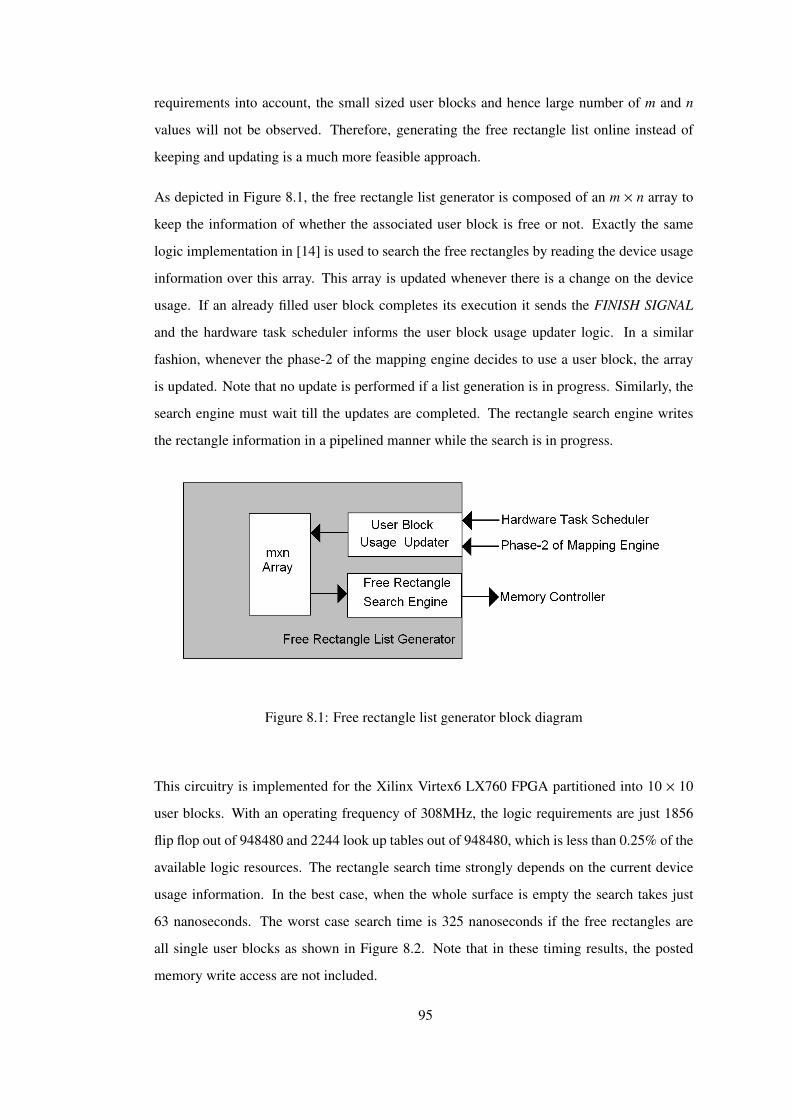
requirements into account, the small sized user blocks and hence large number of m and n
values will not be observed. Therefore, generating the free rectangle list online instead of
keeping and updating is a much more feasible approach.
As depicted in Figure 8.1, the free rectangle list generator is composed of an m × n array to
keep the information of whether the associated user block is free or not. Exactly the same
logic implementation in [14] is used to search the free rectangles by reading the device usage
information over this array. This array is updated whenever there is a change on the device
usage. If an already filled user block completes its execution it sends the FINISH SIGNAL
and the hardware task scheduler informs the user block usage updater logic. In a similar
fashion, whenever the phase-2 of the mapping engine decides to use a user block, the array
is updated. Note that no update is performed if a list generation is in progress. Similarly, the
search engine must wait till the updates are completed. The rectangle search engine writes
the rectangle information in a pipelined manner while the search is in progress.
Figure 8.1: Free rectangle list generator block diagram
This circuitry is implemented for the Xilinx Virtex6 LX760 FPGA partitioned into 10 × 10
user blocks. With an operating frequency of 308MHz, the logic requirements are just 1856
flip flop out of 948480 and 2244 look up tables out of 948480, which is less than 0.25% of the
available logic resources. The rectangle search time strongly depends on the current device
usage information. In the best case, when the whole surface is empty the search takes just
63 nanoseconds. The worst case search time is 325 nanoseconds if the free rectangles are
all single user blocks as shown in Figure 8.2. Note that in these timing results, the posted
memory write access are not included.
95

Figure 8.2: Worst case condition for free list generation circuitry
8.2.2 Phase-1 Circuitry
The functionality of this circuitry is to allocate the most suitable rectangle(s) to a given num-
ber of user blocks. Since the list of free rectangles is kept in memory, phase-1 circuitry just
inputs the number of user blocks needed from the hardware task scheduler. Whenever a region
allocation request is made, this circuitry starts to allocate a region from the sorted rectangle
list and selects the rectangle(s) in a best fit manner. The rectangle select operation just re-
quires scanning of this sorted list and, depending on the required number of user blocks, it
can be finished in a few scan operations.
However, having a sorted rectangle list, according to the sorting rules given in Chapter 6,
requires a much more complex circuitry. Although it is possible to start from a sorted list and
update it with the changes on the reconfigurable device surface, such an implementation will
be more complex. Since the number of user blocks and hence the number of free rectangles
are limited, the sorting process can be repeated every time it is needed with a simpler circuitry.
On average the well known sorting techniques, like merge sort and insertion sort, have O(nlogn)
complexity. During the sorting process, there is no need to insert a free rectangle into the list
if there are better sized rectangles. For example, if the required area size is 8 user blocks and
the list already contains rectangles that are greater or equal to 8 then there is no need to put a
rectangle with size less than 8 into the list and seek for the suitable position for it. In this way,
the sort complexity will become O(n) and just a single flag is sufficient to indicate whether
96

a rectangle with size less than or equal to the requested user block number is already in the
list or not. As sorting requires |width − length| and access point load comparisons, adder and
subtraction blocks are needed in this circuitry.
Although the achieved operating frequency of this circuit is 433MHz, due to memory read
request, the operating frequency is limited by the memory controller used for the storage of the
free rectangle list and sorted list. With today’s dynamic memory architectures it is possible to
provide high bandwidth if the memory access occurs at consecutive addresses. But for random
and single word read/write access too much time is lost due to initial latency. However,
our sorting process requires read and writes to random locations. Therefore the operating
frequency of our circuitry will be very limited if such a dynamic memory is used. Thanks
to FPGAs embedded static RAM based dual port block RAM implementations operating at
400MHz, it is possible to operate the circuit at 400MHz. For this specific FPGA, the logic
requirement of the region allocation process is 1648 flip flops out of 948480, 4456 look up
tables out of 948480 and 1 block RAM out of 1,440. As shown in Figure 8.3, the other port
of the block RAM is used as the memory interface for free rectangle generator circuitry. As
the allocated region is written to a memory for phase-2 access, a separate memory interface
is needed.
Figure 8.3: Region allocation circuitry block diagram
The execution time of this circuitry completely depends on the required number of user blocks
and the number of free rectangles on the FPGA surface. In the best case, when the whole
FPGA surface is empty, the region allocation takes just 9 cycles (22.5 nanoseconds). The
worst case occurs if the required user block is the half of the total user blocks and if the
device usage is similar to Figure 8.2. In this case, for 10 × 10 user block partitioning, the
region allocation takes 512.5 nanoseconds.
97

8.2.3 Phase-2 Circuitry
In this phase, the physical mapping of the user blocks given by the hardware task scheduler is
performed. As was mentioned above, the user blocks having data dependency are kept in the
memory as a linked list of the given node structure. Therefore, the input port of this circuitry
for the hardware task scheduler is just the front node of the linked list. Note that this is a
sorted linked list with descending value of total traffic demand of the user blocks. The other
input is the allocated region from phase-1 circuitry. Similarly, a linked list is used to represent
the allocated region.
Depending on the type of the allocated region, two physical mapping techniques are used and
hence two different circuitry are designed. Similar to other implementations, due to its fast
and single clock access features the allocated region are kept in a dual port block memory and
one of the ports is connected to memory controller output of the region allocation circuitry. As
shown in Figure 8.4, the other port is connected to both of the physical mapping circuitries,
which are the single rectangle placer and the distributed placer circuitries
Figure 8.4: Physical mapping circuitry block diagram
Just after receiving the physical mapping request, the front node of the linked list representing
the allocated region is checked by both of the circuits and if this is a single node list, only the
single rectangle placer circuitry starts operation. Since mapping of user blocks depend on
the Manhattan distance and the total traffic demand on the path to already placed user blocks,
the communication demand between two neighboring IBCN switches is kept in local memory,
which is a dual port block RAM. Upon receiving the placement request this memory is cleared
98

by just applying a single cycle reset. Starting from the largest rectangle, which is at the front
of the allocated region linked list and from the largest traffic demand user block, which is at
the front of the user block linked list, the physical mapping is done by placing the user block
to the middle of the rectangle area under consideration. Note that the placement requires just
updating the Physical_location field of the user block node in the memory. Then for each
user block in the linked list, the best fit placement is done by first searching for the free user
block with minimum Manhattan distance to the middle of the rectangle area. If there is no
free location on the current rectangle area, the user block is placed on to the middle location
of the next rectangle area in the linked list. If there are more than one such free locations,
the user block with IBCN switch having minimum traffic to the IBCN switch in the middle of
the rectangle area is selected. Upon this selection, traffic demand of the selected user block’s
IBCN switch is updated.
The operation of the single rectangle placer circuitry starts by placing the rectangle onto the
single user block sized virtual rectangle. Starting from the next user block in the linked list,
this virtual rectangle is expanded to minimize the Manhattan distance to the placed user block
with the largest traffic demand to the user block under consideration. This Manhattan distance
is selected such that the virtual rectangle has width and depth to fit to the allocated region. If
there are more than one alternatives for the expansion, the one with the smallest traffic demand
to the largest traffic demand user block is selected. Then the traffic demand of the selected
user block’s IBCN switch is updated. After all user blocks are placed on the virtual rectangle,
Physical_location fields of the user blocks are updated using the given free rectangle area
location on the reconfigurable hardware.
Among all parts of the mapping engine, phase-2 Circuitry is the most logic block consuming
one. The implementation results on Virtex6 LX760 FPGA has shown that two dual port block
RAM, 6842 flip flops out of 948480 and 10832 look up tables out of 948480 is needed and
the achieved operating frequency is 316MHz. When the whole mapping engine is considered,
the total logic demand is 10346 flip flops out of 948480, 17532 look up tables out of 948480,
4 dual port block RAM out of 1440, which represents around 1.5 % of the FPGA resources.
The execution time of phase-2 circuitry completely depends on the allocated region and the
number of user blocks. However, due to search on a larger number of user blocks with the
same Manhattan distance and traffic demand, the single rectangle placer requires more time
99

to complete. For example, the physical mapping takes 1.13 microseconds to place 25 user
blocks onto an allocated region of 5 × 5 user blocks. This time decreases to 221 nanoseconds
for the placement of 8 user blocks onto a region of 3 × 3 user blocks.
8.3 System Area Circuitry Implementation Results
In order to show the logic resource requirement of the computing platform, a complete im-
plementation is given for the SAC. As was discussed before, the SAC is composed of the
reconfigurable hardware operating system circuitry and the host&memory interface. For this
particular Virtex6 LX760 FPGA, the whole SAC implementation is depicted in Figure 8.5.
In this implementation, the IBCN access points (AP) are connected to hardware operating sys-
tem over a shared bus architecture. In order not to stall this shared bus, buffers are employed
in IBCN access points and its size is selected as 64 entries with 10 bits. The external mem-
ory choice for the implemented reconfigurable computing platform is a 72 bit DDR3 SRAM
and 8 bits are used for error checking and correction. Since this FPGA has hard coded PCI
Express IP Core, the connectivity between the host GPP is performed over the PCI Express.
Finally, the internal configuration access port (ICAP) IP is used for the management of the
partial reconfiguration. The resource requirements and the operating frequency of these SAC
components are listed in Table 8.5.
Table 8.5: Circuit size and performance of SAC components on Xilinx Virtex6 LX760
Circuit Logic Requirements PerformanceHWICAP IP [74] Slice FF pairs : 717 out of 948480 32 bit @ 125MHz
Slice LUTs : 900 out of 948480DDR3 SDRAM Slice FF pairs : 5582 out of 948480 72 bit @ 1066MHzController [75] Slice LUTs :5899 out of 948480PCI Express IP [76] Slice FF pairs : 500 out of 948480 x4 lane PCI Express,
Slice LUTs :625 out of 948480 @2.5 / 5GHzIBCN access point Slice FF pairs : 756 out of 948480 374 MHzwith 64x10 bit buffer Slice LUTs :420 out of 948480Hardware Operating Slice FF pairs : 14532 out of 948480 Hardware TaskSystem Slice LUTs :21653 out of 948480 Scheduler @ 274Mhz
Block Ram :12 out of 1440
100

For this particular FPGA, when the reconfigurable hardware is partitioned into 10 × 10 user
blocks, about 5% percent of the FPGA resources are reserved for the SAC implementation.
Since the logic demand for IBCN will be 13%, the remaining 82% of the logic resources are
available for the user’s hardware task implementation.
Figure 8.5: SAC implementation for Xilinx Virtex6 LX760
101

CHAPTER 9
COMPUTATIONAL STUDY
Using our proposed novel reconfigurable computing platform, a substantial level of perfor-
mance improvement may be achieved in terms of effective hardware task circuit size and total
device utilization while providing high level of design flexibility with real time support and
soft task pre-emption for priority based scheduling. In addition, the reconfiguration overhead
may significantly be decreased depending on hardware task parameters. In order to illustrate
these possible improvements, an extensive computational study is performed. Below, our
experimental framework and simulation results are reported.
9.1 Computational Study Results on Reconfigurable Device Utilization
In this subsection, computational study results about reconfigurable resource management and
total device utilization compared to some existing methods are reported. Among these exist-
ing methods, fixed block size approaches are applicable in embedded real time applications
since others suffer from external fragmentation and require de-fragmentation. If one dimen-
sional fixed block partitioning is employed, a shared bus is used as the communication media
in general, which lowers the operating frequency of hardware tasks considerably. Therefore
the comparison is made only between our reconfigurable computing platform proposal and
the two dimensional fixed block size partitioning methods in [20,21].
Our computational study is carried out using a number of embedded systems that are classified
according to the following parameters:
• TSR (task size ratio): ratio of the size of the largest hardware task to the smallest
102

hardware task size.
• EBSR (execution block size ratio): ratio of the size of the largest execution block to
the size of the smallest execution block.
• PF (parallelism factor): ratio of the number of execution blocks working in parallel
to the number of execution blocks in the hardware task. It is in range [0, 1] and is equal
to 1 if all of the execution blocks are working in parallel.
Similar to IBCN and SAC implementation, Xilinx Virtex6 LX760 FPGA is chosen as the
target reconfigurable hardware. The Virtex6 LX760 series device has 118,560 slices, which
is equivalent to around 5.5 million gates when CLB utilization is approximately 60%.
In order to evaluate our model, we calculated ρtotal, e f f ective_size() and improvement in
ρtotal as compared to [20,21] for different embedded system classes. Each embedded system
class is classified by its TS R, EBS R and PF values. In total, 640 embedded system classes
are studied using eight TS R, eight EBS R and ten PF values. In each embedded system class
ρtotal, e f f ective_size() and improvement in ρtotal are calculated for 100 embedded systems
each composed of 1000 randomly generated hardware tasks using a uniform distribution. In
all classes, the minimum size of a hardware task is selected to be 100K gates and minimum
execution block size is selected as 10K gates. Note that, ρtotal and e f f ective_size() are inde-
pendent of reconfiguration time. We have observed that all our results are within 1% vicinity
of the calculated and reported averages using 95% confidence interval.
The communication media used in two dimensional fixed block models in [20,21] is un-
known. We therefore used our IBCN implementation as the communication media in all our
comparison work.
Our computations have shown that ρtotal and e f f ective_size() are almost independent of TS R.
Among eight different values of TS R, the worst e f f ective_size() and ρtotal values are obtained
for TS R = 1.75 and therefore we present here the variation of these parameters against par-
allelism factor PF and execution block ratio EBS R for TS R = 1.75 case only. In Appendix,
the computational results for other TS R values are reported.
Figure 9.1 shows that if the tasks are not highly parallel (having smaller PF) the hardware task
circuitry can be executed on a smaller area on the reconfigurable hardware. An approximate
103

reduction to 25% percent of the whole task circuit size is achieved in e f f ective_size() when
PF = 0.1 and EBS R = 1. The circuit size should ideally reduce to 10% in this case, however
our proposal diverts from the ideal due to pre-fetching for shortest turnaround time and due
to non-integer multiple size of the user block size compared to actual execution block sizes.
Increasing PF increases the circuit size and it becomes 1 when PF is approximately 0.5. The
value of e f f ective_size() reaches to at most 1.18 when PF is higher, which means that we
need a slightly larger (approximately 18%) circuit area compared to the ideal requirement for
highly parallel tasks due to fragmentation during the bin packing process.
Figure 9.1: Ratio of e f f ective_size() to whole circuit size with respect to PF for TS R = 1.75case
For the embedded system class with PF = 1 and EBS R = 1, ρtotal is observed to be 3.24
at most (see Figure 9.2). Since we have reduction in hardware task circuit sizes, ρtotal is
more than unity. With increasing EBS R, ρtotal slightly decreases and reaches to 2.44 for
EBS R = 5. Similar to e f f ective_size(), increasing PF results in a decrease in ρtotal and the
minimum utilization is 79% in our computational study. Therefore, we conclude that 21%
of the reconfigurable hardware resources are wasted in the worst case because of our IBCN
implementation and fragmentation due to the bin packing process.
We observed that the effect of TS R is negligible for both e f f ective_size() and ρtotal. How-
104
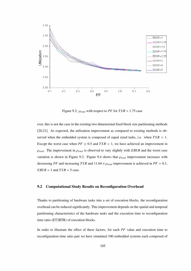
Figure 9.2: ρtotal with respect to PF for TS R = 1.75 case
ever, this is not the case in the existing two dimensional fixed block size partitioning methods
[20,21]. As expected, the utilization improvement as compared to existing methods is ob-
served when the embedded system is composed of equal sized tasks, i.e. when TS R = 1.
Except the worst case when PF ≥ 0.5 and TS R = 1, we have achieved an improvement in
ρtotal. The improvement in ρtotal is observed to vary slightly with EBS R and the worst case
variation is shown in Figure 9.3. Figure 9.4 shows that ρtotal improvement increases with
decreasing PF and increasing TS R and 11.64 × ρtotal improvement is achieved in PF = 0.1,
EBS R = 1 and TS R = 5 case.
9.2 Computational Study Results on Reconfiguration Overhead
Thanks to partitioning of hardware tasks into a set of execution blocks, the reconfiguration
overhead can be reduced significantly. This improvement depends on the spatial and temporal
partitioning characteristics of the hardware tasks and the execution time to reconfiguration
time ratio (ET2RTR) of execution blocks.
In order to illustrate the effect of these factors, for each PF value and execution time to
reconfiguration time ratio pair we have simulated 100 embedded systems each composed of
105

Figure 9.3: Ratio of ρtotal with our proposal to that of 2D fixed partitioning [20,21] againstPF for TS R = 1
Figure 9.4: Ratio of ρtotal with our proposal to that of 2D fixed partitioning [20,21] againstTS R for EBS R = 1
106

1000 hardware tasks. The number of execution blocks for a task is randomly selected between
100 and 200 in a uniformly distributed manner. In a similar fashion, the execution block size
is randomly selected to be between 10K and 40K gates. The device under consideration for
this computational study is also Virtex6 LX760 FPGA.
Figure 9.5 presents the average achieved reconfiguration overhead in terms of percentage of
reconfiguration time to total task turnaround time.
Figure 9.5: Reconfiguration overhead as percentage of total task turn around time variationagainst ET2RTR for different values of PF
The achieved reconfiguration overhead is presented in an alternative form as the percentage
of reconfiguration overhead without task partitioning in Figure 9.6. As expected, a great
improvement is achieved in reconfiguration overhead for hardware tasks with small PF values.
Even for highly parallel tasks, for which PF is greater than 0.5, a certain level of improvement
is still possible.
107

Figure 9.6: Achieved reconfiguration overhead as percentage of reconfiguration overheadwithout task partitioning versus ET2RTR for different values of PF
9.3 Comparison Results on Device Utilization and Reconfiguration Overhead
As was stated earlier, the idea of partitioning a hardware task into set of sub-tasks with the
aim of minimizing the reconfiguration time overhead was also used by Resano et al. [26,27].
While providing a higher device utilization our reconfigurable computing platform may have
a higher reconfiguration overhead as compared to [26,27] due to our packing process.
A comparative study on the test set used previous in the section is performed and the results
are presented in Figures 9.7 and 9.8. As shown in Figure 9.7, with increasing execution time
to reconfiguration time ratio, the reconfiguration overhead is increased and reaches to 4×
compared to [26,27]. However, for a large value of execution time to reconfiguration time
ratio, this drawback is still acceptable because the corresponding reconfiguration overhead,
which can be deduced using Figure 9.5, is very small. Despite such a small reconfiguration
overhead increase, as depicted in Figure 9.8 our method provides around 1.6× utilization
improvement as compared to [26,27].
108

Figure 9.7: Ratio of reconfiguration overhead our proposal to reconfiguration overhead with[26,27] against PF
Figure 9.8: Ratio of ρtotal with our proposal to that of [26,27] against PF
109

CHAPTER 10
APPLICATION EXAMPLE
A candidate application is chosen our complete reconfigurable computing platform solution.
This application is an image and sensor fusion application for an airborne defense system. As
depicted in Figure 10.1, four thermal-CCTV camera pairs mounted on turret and an external
airborne defense radar are used to detect and track airborne threats such as aircraft fighters,
helicopters and missiles.
Figure 10.1: Application example: Image and sensor fusion to detect and track airbornethreats
110

In addition to running fusion, detection and tracking algorithms, the computing platform in
this application has the following functionalities. Airborne defense radar provides its output
over a radio network in JPEG2000 compressed format due to its low latency requirement, due
to the need for resilience against errors and due to keeping a balance between compression
and quality. Hence in this application, the computing platform performs JPEG2000 decoding
of the radar data. The video received from thermal and CCTV camera pairs are compressed
(encoded) in MPEG-4 format for storage. In the test mode or training mode, instead of using
live video from thermal and CCTV camera pairs, this locally stored video in MPEG-4 format
is then decoded. Finally, the detection and tracking information is sent in JPEG2000 format
over a radio link to the information center.
For the system described above, our complete reconfigurable computing platform solution
proposal is a good candidate due to its support for true multitasking, its design flexibility,
short turnaround time and efficient device utilization. As shown in Figure 10.2, a possible
underlying hardware is composed of a PowerPC based dual core processor MPC8640D, a
Xilinx Spartan6 series FPGA used for glue logic and connectivity and a Xilinx Virtex6 LX760
FPGA used as the actual reconfigurable hardware resource.
The system operates as follows: A synchronizer in Spartan3 FPGA sends a trigger signal to
the application software running on PowerPC. Depending on the source selection, the appli-
cation software initially schedules MPEG-4 encoders or decoders and JPEG2000 decoder to
Virtex6 FPGA. When frame decoding is completed, the application software schedules;
• a fusion algorithm selected among four fusion algorithms based on availability and
latency of radar information and environmental conditions such as fog, rain, snow, day
and night,
• two different target detection algorithms selected among five detection algorithms based
on environmental conditions and detection information of the previous frame and
• up to four instances of tracking algorithms selected among three tracking algorithms
based on the number of tracked targets and target types.
Note that up to seven tasks are scheduled to operate simultaneously. Tracking and detection
algorithms process the output of the fusion algorithm of the previous stage. With the comple-
tion of these tasks, the application software is then notified and the JPEG2000 encoding of
111

Figure 10.2: Complete reconfigurable computing solution for the application example
112

the image with a track symbol on tracked targets is initiated. Finally, the application software
is informed about the completion of JPEG2000 encoding whenever it happens.
The circuit parameters for MPEG-4 encoder and decoder are estimated by mapping already
reported results in the literature to our target FPGA. The circuit for fusion, detection and
tracking are obtained by converting the MATLAB codes to VHDL. The circuit sizes of the
algorithms are obtained after synthesis and placement/routing with Xilinx ISE tools and the
execution times are calculated using post timing analysis. Similarly, circuit sizes and exe-
cution times for JPEG2000 encoder and decoder are obtained by re-synthesizing an already
existing design for Virtex-6. The circuit size, execution time, reconfiguration time, effective
circuit size and achieved reconfiguration time of each task is listed in Table 10.1.
Table 10.1: Parameters of individual hardware tasks in the application example
Task Circuit Execution Reconfiguration Effective AchievedName Size Time Time Circuit Reconfiguration
(slice) (msec) (msec) Size Time(slice) (msec)
MPEG-4 4742 2.34 1.749 1440 0.342Decoder [77]MPEG-4 8622 4.81 3.181 4320 0.719Encoder [78]JPEG2000 5256 2.62 1.941 2880 0.31DecoderJPEG2000 6049 3.25 2.232 2880 0.468EncoderFusion-1 27106 14.3 10.002 12960 2.543Fusion-2 14203 16.1 5.241 7920 0.692Fusion-3 19932 11.7 7.355 8640 1.345Fusion-4 23335 14.2 8.611 12240 2.576Detection-1 24552 15.1 9.06 12240 1.094Detection-2 17620 12 6.502 10800 1.272Detection-3 19652 14.2 7.252 8640 1.338Detection-4 23299 12.7 8.597 12960 1.17Detection-5 18363 15.3 6.776 10080 1.579Tracking-1 10753 5.5 3.968 2880 0.763Tracking-2 13340 6.1 4.922 7920 0.856Tracking-3 11304 5.8 4.171 7200 0.905
Note that the in Table 10.1, circuit size is the number of FPGA slices needed to implement
113

the associated hardware task as a single circuit. Similarly, the reconfiguration time is the time
needed to load the whole task circuitry without any partitioning. We then calculated, for this
particular FPGA, the effective circuit size, which represents the maximum area needed at any
instance for the task to be executed. Also the achieved reconfiguration overhead is calculated
taking the partial reconfiguration time and the mapping decision time into consideration.
For this application, our user block size selection heuristic has found that the FPGA surface
should be partitioned in 12 × 12 user blocks each having a size of 720 slices in the shape of
40CLB × 9CLB and the device utilization has turned out to be 1.85. Without using the pro-
posed reconfigurable computing platform, the application example, described above, needs
551K slices and will have a maximum frame processing time of 24.16 milliseconds in the
worst case. Thanks to partial reconfigurability concept and our novel platform proposal that
the resource demand is reduced to 69K slices and the worst case processing time is just in-
creased to 28.59 milliseconds which means that 30 frames per second processing speed can
be used. This time includes the execution time, mapping decision and reconfiguration time
of the user blocks. Note that, the time overhead due to IBCN communication and the shared
memory access is not taken into account as it requires a very complicated simulation study.
114

CHAPTER 11
CONCLUSIONS AND FUTURE WORK
In this chapter, conclusions of this thesis work are stated. A brief discussion on the contri-
butions made by this dissertation is given. In addition, a discussion on the future work to
improve and extend the application area of the presented reconfigurable computing platform
is presented.
11.1 Contributions
In this thesis work, we present a complete reconfigurable computing platform for embedded
applications. This reconfigurable computing platform is developed to give design flexibility
similar to software development for conventional computing with general purpose processors.
The proposed reconfigurable computing platform is a combination of a universal reconfig-
urable hardware, which is very similar to commercial FPGA devices, and a general purpose
processor. The application programmer is allowed to design the applications with both hard-
ware and software tasks. With a specially designed operating system architecture, the details
of the underlying hardware is hidden from the application programmer and high level oper-
ating system services are provided to both software and hardware tasks. In addition, with its
deterministic response time, our reconfigurable computing platform proposal is well suited
for embedded applications with real time requirements.
In our reconfigurable computing platform, the application programmer is responsible to give
the hardware task only. For this purpose, we have introduced a novel hardware tasks model
and this task model requires a hardware task to be partitioned by the application program-
mer into sub tasks, which is called execution blocks, using both temporal and spatial par-
115

titioning processes. Thanks to this novel hardware task model, our proposal requires less
reconfigurable hardware area for implementing the circuitry of the hardware task and the re-
configuration time overhead is kept at low level, which results in short task turnaround time.
In addition, by starting and stopping hardware tasks at this execution block boundaries, our
reconfigurable computing platform supports preemption for priority based scheduling.
In the proposed reconfigurable computing platform the reconfigurable hardware is completely
managed by the hardware operating system and a novel two dimensional surface partition
process is used. The proposed partitioning technique allocates fixed size regions for hardware
task implementation and provides an interconnection media for both external memory access
and communication between fixed size regions. With this interconnection media, the execu-
tion blocks of hardware tasks can be placed onto non-contiguous areas on the reconfigurable
hardware and hence the whole reconfigurable hardware surface can be used in an efficient
manner.
It has been observed that the surface partitioning parameters determine the reconfigurable
hardware utilization and hence a mathematical model for selecting the the surface partitioning
parameters is given. A greedy heuristic technique employing bin packing process is used to
solve this problem and it has been shown that the gap between the results of our greedy
heuristic and the relaxed upper bound is just 4.5%.
As an interconnection media, a special two dimensional mesh NoC architecture with worm-
hole routing is designed. For this purpose a special wormhole switch architecture is developed
and its implementation results has shown that a very high bandwidth can be offered with low
logic demand. For Xilinx Virtex6 LX760, when the FPGA surface is partitioned into 10 × 10
fixed blocks, only 13% of the logic resources are used for this NoC implementation and 62.4
GByte/s aggregate bandwidth is achieved.
The performance of reconfigurable computing platform proposal has been evaluated with an
extensive computational study in terms of reconfigurable hardware resource management and
reconfiguration time overhead. It has been shown that our solution has superior performance
in both reconfigurable hardware utilization and reconfiguration time overhead but of course
depending on the embedded system parameters. When compared to existing two dimensional
surface partitioning techniques [20,21], in which the hardware task is loaded onto a contigu-
ous area, depending on the sizes of the hardware task and the number of execution blocks
116
required to work in parallel up to 11.64 times improvement is achieved in reconfigurable
hardware utilization. Similarly, depending on the number of execution blocks required to
work in parallel, the execution time and the circuit size, the reconfiguration time overhead is
decreased up to 3% of task execution time. When compared to existing techniques [26,27],
in which the hardware tasks are partitioned into fixed size sub-tasks, our computing platform
achieves a bit larger reconfiguration time overhead. However, the reconfigurable hardware
utilization in our proposal is around 1.6 times that of [26,27].
In our reconfigurable computing platform proposal, application programmer is responsible to
partition his/her hardware task into execution blocks. The partitioning process must be done
considering both temporal and spatial partitioning and it is allowed to have execution blocks
with data dependency. Since this data dependency is handled by our NoC, the execution time
of the hardware task will be increased due to the NoC’s latency. Hence it is not recommended
to have a partition with high rate data dependency because such partitioning may result in
unacceptable increase in the execution time. In case such a partitioning still occurs, we pro-
pose, as a remedy, an online two phase ad-hoc mapping technique that finds suitable locations
for the execution blocks to keep the communication overhead on the NoC as low as possible.
The proposed ad-hoc solution is a multi objective mapping technique, which tries to minimize
the store and forward latency, minimize path blocking due to wormhole routing and balance
external memory access.
Finally, a real life application, which is an image and sensor fusion application to detect
and track airborne threats, is solved using our reconfigurable computing platform. For this
specific application, the reconfigurable hardware resource requirement is reduced to 14% of
the original resource requirement with just a 19% increase in execution time.
11.2 Future Work
In the proposed reconfigurable computing platform, the application programmer responsibil-
ity is only to partition the application into a set of execution blocks. This partitioning process
affects both device utilization and task turn around time. In addition, the IBCN communica-
tion latency increases if the execution blocks have too much data dependency. As future work,
a partitioning technique can be developed so that the application programmer is just respon-
117

sible to write the application in a hardware description language. This partitioning technique
will take both the temporal and spatial behaviors of the given task to generate the execution
blocks to maximize the computing platform performance.
Within the scope of this thesis work, the hardware task scheduler and the associated compo-
nents are designed to support the scheduling of hardware tasks in any order and for unknown
arrival times. In some embedded applications, it is possible to know the scheduling sequence
and arrival times. Therefore, it is possible to improve the task turn around time and hence the
system performance with an offline optimization process. As future work, an offline mapping
and scheduling technique can be developed to find the physical location and mapping of the
user blocks that minimizes the embedded system’s response time.
118

REFERENCES
[1] G. Estrin, Organization of computer systems-the fixed plus variable structure computer,Proc. of Western Joint Computer Conference, (1960) 33-40.
[2] G. Lu, M. Lee, H. Singh, N. Bagherzadeh, F. Kurdahi, E. Filho, MorphoSys: a recon-figurable processor targeted to high performance image application, Proc. 6th Reconfig-urable Architectures Workshop RAW, (1999) 661-669.
[3] X. Tang, M. Aalsma, R. Jou, A compiler directed approach to hiding configuration la-tency in chameleon processors, International Conference on Field Programmable Logicand Applications FPL, (2000) 29-38.
[4] S.R. Alam, P.K. Agarwal, M.C. Smith, J.S. Vetter, D. Caliga, Using FPGA devices toaccelerate biomolecular simulations, Computer, vol. 40. No. 3, (2007) 66-73.
[5] E. Grayver, B. Daneshrad, A reconfigurable 8 GOP ASIC architecture for high-speeddata communications, IEEE Journal on Selected Areas in Communications, vol. 18, no.11, (2000) 2161-2171.
[6] R.W. Duren, R.J. Marks, P.D. Reynolds, M.L. Trumbo, Real-time neural network inver-sion on the SRC-6e reconfigurable computer, IEEE Transactions on Neural Networks,vol. 18, no. 3, (2007) 889-901.
[7] M.D. Galanis, G. Dimitroulakos, C.E. Goutis, Speedups and energy reductions frommapping DSP applications on an embedded reconfigurable system, IEEE Transactionson Very Large Scale Integration (VLSI) Systems, vol. 15, no. 12, (2007) 1362-1366.
[8] Cray Inc., http://www.cray.com/, last visited on August 2011.
[9] SGI Inc., http://www.sgi.com/, last visited on August 2011.
[10] Q. Deng, S. Wei, H. Xu, Y. Han, G. Yu, A reconfigurable RTOS with HW/SW co-scheduling for SOPC, Second International Conference on Embedded Software andSystems, (2005) 1-6
[11] H. Walder, M. Platzner, Non-preemptive multitasking on FPGAs task placement andfootprint transform, Proc. of Int. Conf. on Engineering of Reconfigurable Systems andAlgorithms, (2002) 24-30.
[12] K. Bazargan, R. Kastner, M. Sarrafzadeh, Fast template placement for reconfigurablecomputing systems, IEEE Design and Test of Computers, (2000) 68-83.
[13] H. Walder, C. Steiger, M. Platzner, Fast online task placement on FPGAs: free space par-titioning and 2D-hashing, Proc. of Int. Parallel and Distributed Processing Symposium,(2003) 178-185.
119

[14] Z. Gu, W. Liu, J. Xu, J. Cui, X. He, Q. Deng, Efficient algorithms for 2D area man-agement and online task placement on runtime reconfigurable FPGAs, Microprocessorsand Microsystems, vol. 33, no. 5-6, (2009) 374-387.
[15] M. Handa, R. Vemuri, An efficient algorithm for finding empty space for online FPGAplacement,Design Automation Conference, (2004) 960-965.
[16] O. Diessel, H. ElGindy, M. Middendorf, H. Schmeck, B. Schmidt, Dynamic schedulingof tasks on partially reconfigurable FPGAs, IEE Proceedings on Computers and DigitalTechniques, vol. 147, no. 3, (2002) 181-188.
[17] G. Brebner, O. Diessel, Chip-based reconfigurable task management, Lecture Notes inComputer Science, Springer, vol. 2147, (2001), 182-191.
[18] H. Walder, M. Platzner, Online scheduling for block-partitioned reconfigurable hard-ware, in Proc. of the IEEE Design, Automation and Test in Europe Conference andExhibition, (2003) 290-295.
[19] H. Walder, M. Platzner, A runtime environment for reconfigurable hardware operatingsystems, Lecture Notes in Computer Science, Springer, vol. 3203, (2004) 831-835.
[20] T. Marescaux, A. Bartic, V. Dideriek, S. Vernalde, R. Lauwereins, Interconnection net-works enable fine-grain dynamic multi-tasking on FPGAs, Proc. of 12th Int. Conf. onField-Programmable Logic and Applications, (2002) 795-805.
[21] P. Merino, M. Jacome, J.C. Lopez, A methodology for task based partitioning andscheduling of dynamically reconfigurable systems, Proc. of IEEE Symp. on FPGAs forCustom Computing Machines, (1998) 324-325.
[22] K. Compton, L. Zhiyuan, J. Cooley, S. Knol, S. Hauck, Configuration relocation and de-fragmentation for run-time reconfigurable computing, IEEE Transactions on Very LargeScale Integration (VLSI) Systems, vol. 10, no. 3, (2002) 209-220.
[23] M.J. Wirlhlin, B.L. Hutchings, A dynamic instruction set computer, Proc. of IEEESymp. on FPGAs for Custom Computing Machines, (1995) 99-107.
[24] S. M. Scalera, J. R. Vazquez, The design and implementation of a context switchingFPGA, IEEE Symposium on Field-Programmable Custom Computing Machines, (1998)78-85.
[25] L. Bauer, M. Shafique, J. Henkel, A computation and communication infrastructure formodular special instructions in a dynamically reconfigurable processor, Proc. of Int.Conference on Field Programmable Logic and Applications, (2008) 203-208.
[26] J. Resano, D. Verkest, D. Mozos, S. Vernalde, F. Catthoor, A hybrid design-time run-time scheduling flow to minimize the reconfiguration overhead of FPGAs, Microproces-sors and Microsystems, vol. 28, no. 5-6, (2004) 291-301.
[27] J. Resano, D. Mozos, D. Verkest, F. Catthoor, A reconfiguration manager for dynami-cally reconfigurable hardware of FPGAs, IEEE Design Test of Computers, vol. 22, no.5, (2005) 452-460.
[28] G.J. Brebner, A virtual hardware operating system for the Xilinx XC6200, in R. W.Hartenstein and M. Glesner, Eds. Lecture Notes in Computer Science, Springer-Verlag,vol. 1142, (1997) 327-336.
120

[29] G.B. Wigley, D.A. Kearney, D. Warren, Introducing ReConfigME: an operating systemfor reconfigurable computing, Lecture Notes in Computer Science, Springer, vol. 2438,(2002) 687-697.
[30] M. Götz, A. Rettberg, C.E. Pereira, A run-time partitioning algorithm for RTOS on re-configurable hardware, Lecture Notes in Computer Science, Springer, vol. 3824, (2005)469-478.
[31] M. Edwards, P. Green, Run-time support for dynamically reconfigurable computing sys-tems, Journal of Systems Architecture, vol. 49, no. 4-6, (2003) 267-281.
[32] K. Danne, R. Muhlenberg, M. Platzner, Executing hardware tasks on dynamically re-configurable hardware under real-time conditions, Proc. of Int. Conference on FieldProgrammable Logic and Applications, (2006) 1-6.
[33] M. Ullmann, M. Hubner, B. Grimm, J. Becker, On-demand FPGA run-time system fordynamical reconfiguration with adaptive priorities, Lecture Notes in Computer Science,Springer, vol. 3203, (2004) 454-463.
[34] H. Kwork, H. So, R. Brodersan, A unified hardware software runtime environment forFPGA based reconfigurable computers using BORPH, ACM Transactions on EmbeddedComputing Systems, vol. 7, no. 2, (2008) 1-28.
[35] G.B. Wigley, D.A. Kearney, Research issues in operating systems for reconfigurablecomputing, in: Proc. of the Int. Conference on Engineering of Reconfigurable Systemsand Algorithms, (2002) 10-16.
[36] Xilinx MicroBlaze soft processor core, http://www.xilinx.com/tools/microblaze.htm, last visited on August 2011.
[37] Altera Nios II processor, http://www.altera.com/devices/processor/nios2/ni2-index.html, last visited on August 2011.
[38] Xilinx Virtex-5 series FPGA, http://www.xilinx.com/support/documentation/virtex-5.htm, last visited on August 2011.
[39] Wind River VxWorks RTOS, http://www.windriver.com/products/vxworks/,last visited on August 2011.
[40] Wind River RTLinuxFree, http://www.rtlinuxfree.com/, last visited on August2011.
[41] Altera Stratix IV FPGA ALM Logic Structure’s 8-Input Fracturable LUT,http://www.altera.com/products/devices/stratix-fpgas/stratix-iv/overview/architecture/stxiv-alm-logic-structure.html, last visited onAugust 2011.
[42] Xilinx Virtex-4 series FPGA, http://www.xilinx.com/support/documentation/virtex-4.htm, last visited on August 2011.
[43] Xilinx Partial Reconfiguration User Guide, http://www.xilinx.com/support/documentation/sw_manuals/xilinx12_1/ug702.pdf, last visited on August2011.
121

[44] E.G. Coffman, M.R. Garey, D.S. Johnson, An application of bin-packing to multi-machine scheduling, SIAM Journal of Computing, vol. 7, no. 1, (1978) 1-17.
[45] N.D.G. Jatinder, C.H. Johnny, A new heuristic algorithm for the one-dimensional bin-packing problem, Production Planning & Control, vol. 10, no. 6, (1999) 598-603.
[46] A. Scholl, R. Klein, C. Jurgens, BISON: A fast hybrid procedure for exactly solving theone-dimensional bin-packing problem, Computers & Operations Research, vol. 24, no.7, (1997) 627-645.
[47] K. Fleszar, K.S. Hindi, New heuristics for one-dimensional bin-packing, Computers &Operations Research, vol. 29, no. 7, (2002) 821-839.
[48] C.F.A. Alvim, C.C. Ribiero, F. Glover, J. D. Aloise, A hybrid improvement heuristic forthe one-dimensional bin packing problem, Journal of Heuristics, vol. 10, no. 2, (2004)205-229.
[49] K. Loh, Weight annealing heuristics for solving bin packing and other combinatorial op-timization problems: concepts, algorithms and computational Results, Doctoral Thesis,University of Maryland at College Park, 2006.
[50] W. J. Dally, B. Towles, Route packets,not wires: On-chip interconnection networks,Proc. of Design Automation Conferance, (2001) 684-689.
[51] L.M. Ni, P.K. McKinley, A survey of wormhole routing techniques in direct networks,IEEE Computer (1993) 62-76.
[52] F. Moraes, N. Calazans, A. Mello, L. M’oller, L. Ost, HERMES: An infrastructure forlow area overhead packet-switching networks on chip, IEEE VLSI Integration, (2004)69-93
[53] M. Majer, C. Bobda, A. Ahmadinia, J. Teich, Packet routing in dynamically changingnetworks on chip, Proc. of the 19th IEEE Int. Parallel and Distributed Processing Sym-posium, (2005) 154-161.
[54] T. Pionteck, C. Albrecht, R. Koch, A dynamically reconfigurable packet-switchednetwork-on-chip, Proc. of the Design Automation & Test in Europe Conference, (2006)1-4.
[55] S. Corbetta, V. Rana, M.D. Santambrogio, D. Sciuto, A light-weight network-on-chiparchitecture for dynamically reconfigurable systems, Prof. of Int. Conference on Em-bedded Computer Systems: Architectures, Modeling and Simulation, (2008) 49-56.
[56] S. Jovanovic, C. Tanougast, C. Bobda, S. Weber, CuNoC: A dynamic scalable com-munication structure for dynamically reconfigurable FPGAs, Microprocessors and Mi-crosystems, vol. 33, no. 3, (2009) 24-36.
[57] K. Faraydon, N. Anh, D. Sujit, An interconnect architecture for networking systems onchips, IEEE Micro, vol. 22, no. 5, (2002) 36-45.
[58] P.P. Pande, C. Grecu, A. Ivanov, R. Saleh, Design of a switch for network on chipapplications, Proc. of the Int. Symposium on Circuits and Systems, (2003) 217-220.
122

[59] P. Guerrier, A. Greiner, A generic architecture for on-chip packet-switched interconnec-tions, Proceedings of the Conference on Design, Automation and Test in Europe, (2000)250-256.
[60] J. Hu, R. Marculescu, Exploiting the routing flexibility for energy/performance awaremapping of regular NoC architectures, Design Automation and Test in Europe Confer-ence and Exhibition, (2003) 688-693.
[61] J. Hu, R. Marculescu, Energy and performance aware mapping of regular NoC archi-tectures, IEEE Transactions on Computer-Aided Design of Integrated Circuits and Sys-tems, (2005) 551-562.
[62] T. Lei, S. Kumar, A two-step genetic algorithm for mapping task graphs to a network onchip architecture, Proceedings of the Euromicro Symposium on Digital System Design,(2003) 180-187.
[63] S. Murali, G. D. Micheli, Bandwidth-constrained mapping of cores onto NoC archi-tectures, Design, Automation and Test in Europe Conference and Exhibition, (2004)1530-1591
[64] G. Ascia, V. Catania, M. Palesi, Multi-objective mapping for mesh-based NoC architec-tures, International Conference on Hardware/Software Codesign and System Synthesis(2004) 182-187.
[65] K. Srinivasan, K. S. Chatha, A technique for low energy mapping and routing innetwork-on-chip architectures, Proceedings of the International Symposium on LowPower Electronics and Design, (2005) 387-392.
[66] A. Hansson, K. Goossens, A. Radulescu, A unified approach to constrained map-ping and routing on network-on-chip architectures, International Conference on Hard-ware/Software Codesign and System Synthesis (2005) 75-80.
[67] V. Nollet, T. Marescaux, P. Avasare, D. Verkesty, J. Y. Mignolet, Centralized Run-Time Resource Management in a Network-on-Chip Containing Reconfigurable Hard-ware Tiles, Proceedings of IEEE Design Automation Test Europe, (2005) 234-239.
[68] C.L. Chou, R. Marculescu, User-aware dynamic task allocation in Networks-on-Chip,Proceedings of. Design and Automation Test, (2008) 1232-1237.
[69] C.L. Chou, R. Marculescu, Run-Time Task Allocation Considering User Behavior inEmbedded Multiprocessor Networks-on-Chip, IEEE Transaction on Computer AidedDesign of Integrated Circuits and Systems, (2010) 78-91.
[70] C. Steiger, H. Walder, M. Platzner, Operating systems for reconfigurable embedded plat-forms: online scheduling of real-time tasks, IEEE Transactions on Computers, vol. 53,no. 11, (2004) 1393-1407.
[71] W. Qiu, B. Zhoul, Y. Chen, C. Peng, Fast on-line real-time scheduling algorithm forreconfigurable computing, Proc. of the 9th Int. Conference on Computer Supported Co-operative Work in Design Proceedings, (2005) 793-798.
[72] G. Buttazzo, Hard real-time computing systems: predictable scheduling algorithms andapplications, Real-Time Systems Series, vol. 23, Springer, (2005).
123

[73] Xilinx ISE 12.4, http://www.xilinx.com/support/documentation/dt_ise12-4.htm, last visited on August 2011.
[74] LogiCORE IP XPS HWICAP, DS586 (v 5.00a), http://www.xilinx.com/support/documentation/ip_documentation/xps_hwicap.pdf, last visited on August2011.
[75] Virtex-6 FPGA Memory Interface Solutions Data Sheet, DS186 (v 1.4), http://www.xilinx.com/support/documentation/ip_documentation/ds186.pdf, last vis-ited on August 2011.
[76] LogiCORE IP Virtex-6 FPGA Integrated Block v1.5 for PCI Express, DS715 (v4), http://www.xilinx.com/support/documentation/ip_documentation/v6_pcie_ds715.pdf, last visited on August 2011.
[77] P. Schumacher, K. Denolf, A. Chilira-RUs, R. Turney, N. Fedele, K. Vissers, J. Bormans,A scalable multi-stream MPEG-4 video decoder for conferencing and surveillance ap-plications, Proc. of IEEE Int. Conference on Image Processing, (2005) 886-889.
[78] K. Denolf, A. Chirila-Rus, D. Verkest, Low-power MPEG-4 video encoder design,Proc. of the IEEE Workshop on Signal Processing Systems Design and Implementation,(2005) 284-289.
[79] W. Hu, C. Wang, J.L. Ma, T.Z. Chen, D. Chen, A novel approach for finding candidatelocations for online FPGA placement, IEEE 10th International Conference on Computerand Information Technology (2010) 2509-2515
124

APPENDIX A
COMPUTATIONAL STUDY RESULTS
As was discussed in Chapter 9, an extensive computational study has been carried out to show
how powerful our proposed technique is. Among 8 different task size ratio (TSR), which is
the ratio of the size of the largest hardware task to the size of the smallest hardware task,
only one of them has been reported in the main text and the rest is reported here. A detailed
description of the computational study is given in Chapter 9.
Figure A.1: Ratio of e f f ective_size() to whole circuit size with respect to PF for TS R = 1case
125

Figure A.2: ρtotal with respect to PF for TS R = 1 case
Figure A.3: Ratio of e f f ective_size() to whole circuit size with respect to PF for TS R = 1.25case
126

Figure A.4: ρtotal with respect to PF for TS R = 1.25 case
Figure A.5: Ratio of ρtotal with our proposal to that of 2D fixed partitioning [20,21] againstPF for TS R = 1.25
127

Figure A.6: Ratio of e f f ective_size() to whole circuit size with respect to PF for TS R = 1.5case
Figure A.7: ρtotal with respect to PF for TS R = 1.5 case
128

Figure A.8: Ratio of ρtotal with our proposal to that of 2D fixed partitioning [20,21] againstPF for TS R = 1.5
Figure A.9: Ratio of ρtotal with our proposal to that of 2D fixed partitioning [20,21] againstPF for TS R = 1.75
129

Figure A.10: Ratio of e f f ective_size() to whole circuit size with respect to PF for TS R =
2.25 case
Figure A.11: ρtotal with respect to PF for TS R = 2.25 case
130

Figure A.12: Ratio of ρtotal with our proposal to that of 2D fixed partitioning [20,21] againstPF for TS R = 2.25
Figure A.13: Ratio of e f f ective_size() to whole circuit size with respect to PF for TS R = 3case
131

Figure A.14: ρtotal with respect to PF for TS R = 3 case
Figure A.15: Ratio of ρtotal with our proposal to that of 2D fixed partitioning [20,21] againstPF for TS R = 3
132

Figure A.16: Ratio of e f f ective_size() to whole circuit size with respect to PF for TS R = 4case
Figure A.17: ρtotal with respect to PF for TS R = 4 case
133

Figure A.18: Ratio of ρtotal with our proposal to that of 2D fixed partitioning [20,21] againstPF for TS R = 4
Figure A.19: Ratio of e f f ective_size() to whole circuit size with respect to PF for TS R = 5case
134

Figure A.20: ρtotal with respect to PF for TS R = 5 case
Figure A.21: Ratio of ρtotal with our proposal to that of 2D fixed partitioning [20,21] againstPF for TS R = 5
135

CURRICULUM VITAE
PERSONAL INFORMATION
Surname, Name : Say, FatihNationality : Turkish (TC)Date and Place of Birth : 19 February 1980 , VanMarital Status : MarriedPhone : +90 312 592 25 49email : [email protected], [email protected]
EDUCATION
Degree Institution Year of GraduationMSc : METU Electrical and Electronics Engineering, 2005BS : METU Electrical and Electronics Engineering, 2002High School : Kazım Karabekir High School, Van 1997
WORK EXPERIENCE
Year Place Enrollment2002 December- Present : ASELSAN A.S. Senior Expert Engineer2002 June : METU, MEMS&VLSI Team Research Engineer
FOREIGN LANGUAGES
Advanced English
PUBLICATIONS
1. Say, F. and C.F. Bazlamaçcı, "A reconfigurable computing platform for real time em-
bedded applications", Microprocessors and Microsystems, (2011), in press.
2. Bazlamaçcı, C.F. and Say, F. "Minimum concave cost multicommodity network de-
sign", Telecommunication Systems, (2007) 181-203
136