
A RAMAN AND RAYLEIGH SCATTERING STUDY OF ELECTRICAL …
138
The Pennsylvania State University The Graduate School Department of Physics A RAMAN AND RAYLEIGH SCATTERING STUDY OF ELECTRICAL AND PHONON PROPERTIES OF SEMICONDUCTING NANOWIRES A Dissertation in Physics by Qiujie Lu © 2010 Qiujie Lu Submitted in Partial Fulfillment of the Requirements for the Degree of Doctor of Philosophy August 2010
Transcript of A RAMAN AND RAYLEIGH SCATTERING STUDY OF ELECTRICAL …
The Pennsylvania State University
The Graduate School
Department of Physics
A RAMAN AND RAYLEIGH SCATTERING STUDY OF ELECTRICAL AND
PHONON PROPERTIES OF SEMICONDUCTING NANOWIRES
A Dissertation in
Physics
by
Qiujie Lu
© 2010 Qiujie Lu
Submitted in Partial Fulfillment of the Requirements
for the Degree of
Doctor of Philosophy
August 2010
The dissertation of Qiujie Lu was reviewed and approved* by the following:
Nitin Samarth Professor of Physics Dissertation Advisor Chair of Committee
Gerald D. Mahan Distinguished Professor of Physics
Vincent H. Crespi Professor of Physics Professor of Materials Science and Engineering
John V. Badding Professor of Chemistry
Jayanth R. Banavar Distinguished Professor of Physics Head of the Department of Physics
*Signatures are on file in the Graduate School
iii
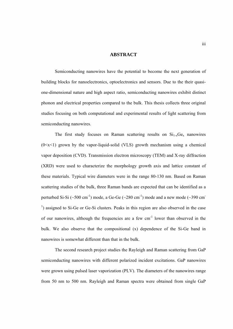
ABSTRACT
Semiconducting nanowires have the potential to become the next generation of
building blocks for nanoelectronics, optoelectronics and sensors. Due to the their quasi-
one-dimensional nature and high aspect ratio, semiconducting nanowires exhibit distinct
phonon and electrical properties compared to the bulk. This thesis collects three original
studies focusing on both computational and experimental results of light scattering from
semiconducting nanowires.
The first study focuses on Raman scattering results on Si1-xGex nanowires
(0<x<1) grown by the vapor-liquid-solid (VLS) growth mechanism using a chemical
vapor deposition (CVD). Transmission electron microscopy (TEM) and X-ray diffraction
(XRD) were used to characterize the morphology growth axis and lattice constant of
these materials. Typical wire diameters were in the range 80-130 nm. Based on Raman
scattering studies of the bulk, three Raman bands are expected that can be identified as a
perturbed Si-Si (~500 cm-1) mode, a Ge-Ge (~280 cm-1) mode and a new mode (~390 cm-
1) assigned to Si-Ge or Ge-Si clusters. Peaks in this region are also observed in the case
of our nanowires, although the frequencies are a few cm-1 lower than observed in the
bulk. We also observe that the compositional (x) dependence of the Si-Ge band in
nanowires is somewhat different than that in the bulk.
The second research project studies the Rayleigh and Raman scattering from GaP
semiconducting nanowires with different polarized incident excitations. GaP nanowires
were grown using pulsed laser vaporization (PLV). The diameters of the nanowires range
from 50 nm to 500 nm. Rayleigh and Raman spectra were obtained from single GaP
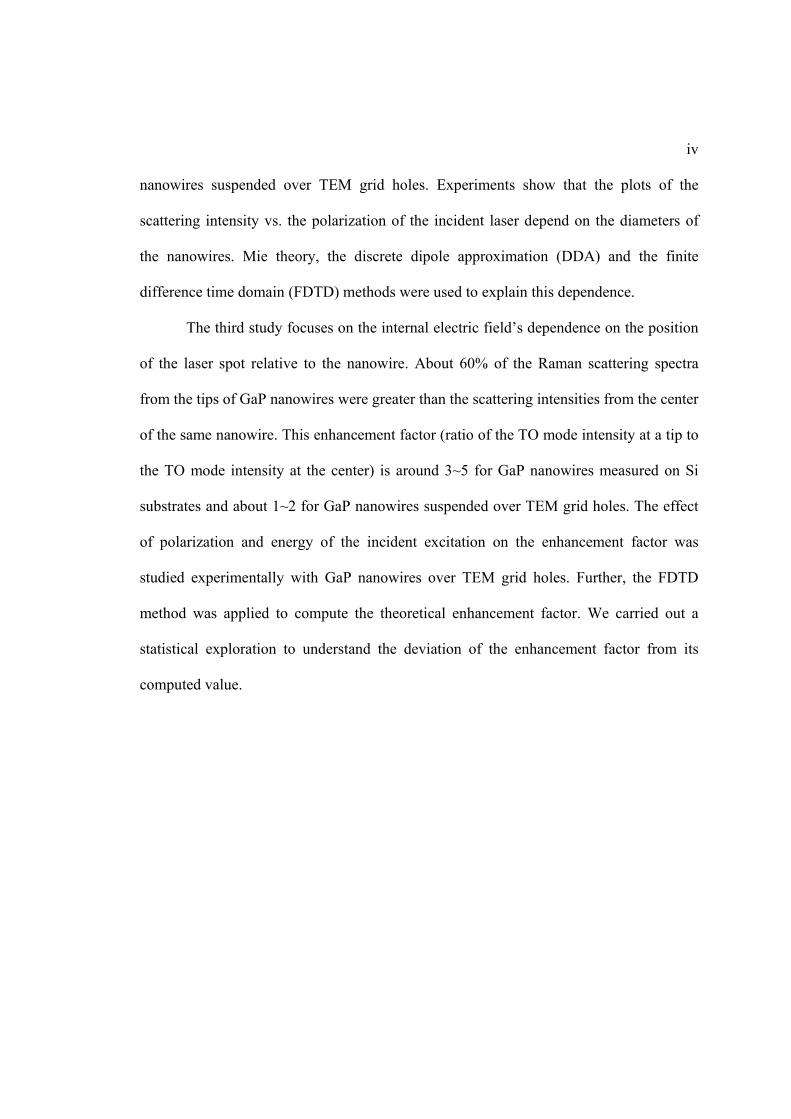
iv
nanowires suspended over TEM grid holes. Experiments show that the plots of the
scattering intensity vs. the polarization of the incident laser depend on the diameters of
the nanowires. Mie theory, the discrete dipole approximation (DDA) and the finite
difference time domain (FDTD) methods were used to explain this dependence.
The third study focuses on the internal electric field’s dependence on the position
of the laser spot relative to the nanowire. About 60% of the Raman scattering spectra
from the tips of GaP nanowires were greater than the scattering intensities from the center
of the same nanowire. This enhancement factor (ratio of the TO mode intensity at a tip to
the TO mode intensity at the center) is around 3~5 for GaP nanowires measured on Si
substrates and about 1~2 for GaP nanowires suspended over TEM grid holes. The effect
of polarization and energy of the incident excitation on the enhancement factor was
studied experimentally with GaP nanowires over TEM grid holes. Further, the FDTD
method was applied to compute the theoretical enhancement factor. We carried out a
statistical exploration to understand the deviation of the enhancement factor from its
computed value.
v
TABLE OF CONTENTS
LIST OF FIGURES ..................................................................................................... vii
LIST OF TABLES ....................................................................................................... xii
ACKNOWLEDGEMENTS ......................................................................................... xiii
Chapter 1 Introduction ................................................................................................. 1
1.1 Motivation of Thesis ....................................................................................... 1 1.2 Structure of Thesis .......................................................................................... 1
Chapter 2 Synthesis of Semiconducting Nanowires in This Thesis ............................ 3
2.1 Vapor-Liquid-Solid (VLS) Growth Mechanism ............................................ 3 2.2 Chemical Vapor Deposition (CVD) Growth Method for Si1-xGex
Nanowires ...................................................................................................... 6 2.3 Pulsed Laser Vaporization (PLV) Growth Method for GaP Nanowires ........ 7 2.4 Chemical Vapor Deposition (CVD) Growth Method for GaP Nanowires ..... 10
Chapter 3 Rayleigh and Raman Scattering .................................................................. 11
3.1 Introduction to Rayleigh and Raman Scattering ............................................. 11 3.2 Classical Theory of Rayleigh and Raman Scattering ..................................... 12 3.3 Quantum Theory of Rayleigh and Raman Scattering ..................................... 15 3.4 Raman Instrumentation ................................................................................... 20
3.4.1 Horiba Jobin Yvon T64000 Raman System ......................................... 21 3.4.2 Renishaw InVia Micro-Raman System ................................................ 24
Chapter 4 Raman Scattering from Si1-xGex Alloy Nanowires ..................................... 26
4.1 Introduction ..................................................................................................... 26 4.2 Experimental Details ...................................................................................... 27 4.3 Results and Discussions .................................................................................. 30 4.4 Conclusion ...................................................................................................... 44
Chapter 5 Computational Methods for E field Scattered by Single Nanowire ............ 46
5.1 Mie Scattering from an Infinitely Long Cylinder ........................................... 47 5.1.1 Incident Electric Field Parallel to the xz Plane .................................... 50 5.1.2 Incident Electric Field Perpendicular to the xz Plane .......................... 52 5.1.3 Conclusion of Mie Scattering ............................................................... 53
5.2 Discrete Dipole Approximation (DDA) Method ............................................ 54
vi
5.2.1 Introduction to DDA method ................................................................ 54 5.2.2 Software for DDA Simulation in This Thesis ...................................... 55
5.3 Finite Different Time Domain (FDTD) Method ............................................ 56 5.3.1 Algorithm of FDTD method ................................................................. 56 5.3.2 Boundary Conditions in FDTD method ............................................... 61 5.3.3 Software for FDTD Method ................................................................. 62
Chapter 6 Antenna Effect in GaP Nanowires .............................................................. 63
6.1 Introduction to the Antenna Effect ................................................................. 63 6.2 Experimental Procedures ................................................................................ 65 6.3 Rayleigh and Raman Antenna Models ........................................................... 67
6.3.1 Introduction to Rayleigh and Raman Antenna Models ........................ 67 6.3.2 Fitting Raman Antenna Patterns with Data from Experimental
Rayleigh Antenna Patterns ..................................................................... 70 6.3.3 Fitting Rayleigh and Raman Antenna Patterns with Computed
Enhancement Tensor .............................................................................. 74 6.4 Discussion and Conclusion ............................................................................. 84
Chapter 7 Hot Tip Effect in GaP Nanowires ............................................................... 89
7.1 Introduction to Hot Tip Effect ........................................................................ 89 7.2 Hot Tip Effect: Experimental Procedures for GaP Nanowires on Si
Substrates ....................................................................................................... 90 7.3 Hot Tip Effect Results for GaP on Si Substrates ............................................ 93 7.4 FDTD Simulation for Hot Tip Effect from GaP Nanowires .......................... 96
7.4.1 GaP Nanowires with Smooth Surface .................................................. 97 7.4.1 GaP Nanowires with Sinusoidal Surface Roughness ........................... 103
7.5 Hot Tip Effect Experimental Procedures for GaP Nanowires on TEM Grids .............................................................................................................. 105
7.6 Results and Discussions for GaP Nanowires on TEM Grids ......................... 107 7.6.1 Hot Tip Effect’s Dependence on Incident Laser’s Polarization ........... 107 7.6.2 Hot Tip Effect’s Dependence on Incident Laser’s Frequency ............. 109 7.6.3 Factors Correlated to Hot Tip Effect .................................................... 111
7.7 FDTD Simulations for E Field Resonance within GaP Nanowires ................ 119 7.8 Conclusion ...................................................................................................... 121
References .................................................................................................................... 122
vii
LIST OF FIGURES
Figure 2-1: In situ TEM images recorded the process of Ge nanowire growth by VLS growth mechanism. (a) Au nanoclusters in solid state at 500 °C; (b) alloying initiates at 800 °C, and Au is in mostly solid state; (c) liquid Au-Ge alloy; (d) the nucleation of Ge nanocrystal on the alloy surface; (e) Ge nanocrystal elongates with further Ge condensation and eventually a wire starts to form; (f), (g) Several other examples of Ge nanowire nucleation; (h), (i) two nucleation events on single alloy droplet [3]. ........................................... 4
Figure 2-2: Three stages in VLS nanowire growth mechanism shown in (a) a schematic illustration; (b) conventional Au-Ge binary phase diagram [3]. .......... 5
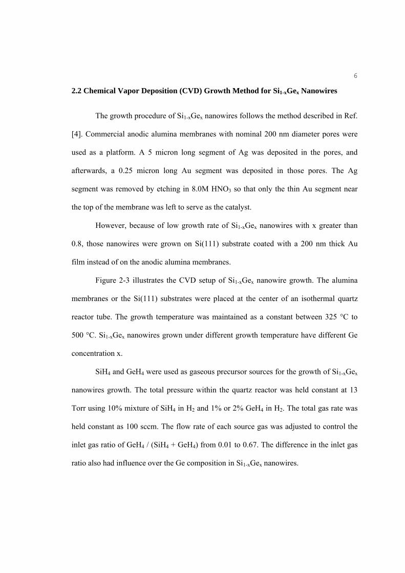
Figure 2-3: Si1-xGex nanowire growth by CVD. .......................................................... 7
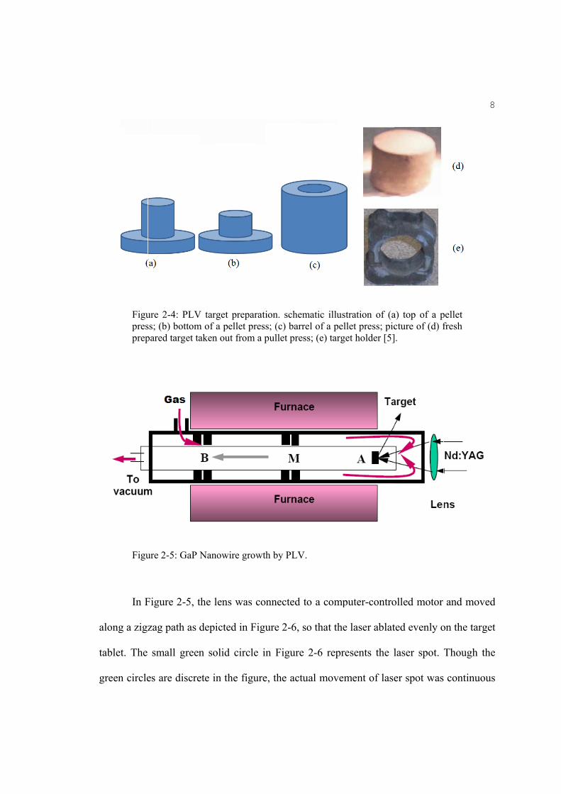
Figure 2-4: PLV target preparation. schematic illustration of (a) top of a pellet press; (b) bottom of a pellet press; (c) barrel of a pellet press; picture of (d) fresh prepared target taken out from a pullet press; (e) target holder [5]. ............ 8
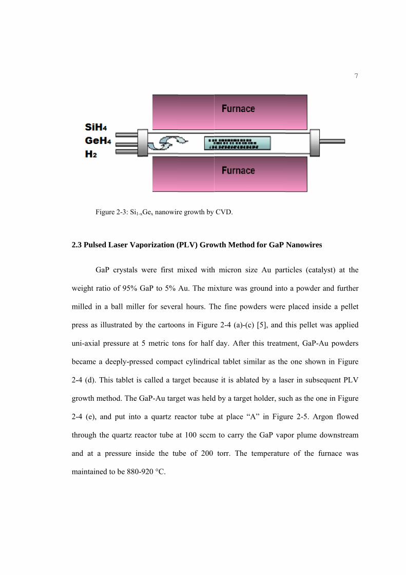
Figure 2-5: GaP Nanowire growth by PLV. ................................................................ 8
Figure 2-6: Illustration of laser spot movement in PLV. ............................................. 9
Figure 2-7: GaP nanowire growth by CVD. ................................................................ 10
Figure 3-1: Four types of Raman scattering: (a) normal (b) pre-resonance (c) discrete resonance (d) continuum resonance Raman scattering. .......................... 18
Figure 3-2: a schematic diagram of Horiba Jobin Yvon T64000 spectrometer internal optics [7]. ................................................................................................. 21
Figure 3-3: optical diagram for (a) double subtractive (b) triple additive mode in Horiba Jobin Yvon T64000 spectrometer [7]. ...................................................... 22
Figure 3-4: Optical diagram of confocal microscope [7]. ............................................ 23
Figure 3-5: A schematic diagram of Renishaw InVia Micro-Raman System internal optics [8]. ................................................................................................. 24
Figure 3-6: Optical diagram of confocal Raman microscopy without pinhole optics [8]. .............................................................................................................. 25
viii
Figure 4-1: (a) Low magnification bright-field TEM image of the Si1-xGex nanowires, the inset shows a SAD pattern from an individual nanowire with growth direction along the [111]. (b) High-resolution TEM image showing the crystalline nature of the Si1-xGex nanowires, the inset is the corresponding Fourier Transform and the white arrow indicates the growth direction ([131]) of this particular nanowire. Most nanowires were observed to grow in the [111] direction. ..................................................................................................... 28
Figure 4-2: Diameter distribution for Si0.88Ge0.12 nanowires. This distribution is typical of all the samples studied here. ................................................................. 29
Figure 4-3: Micro-Raman spectra from seven batches of crystalline Si1-xGex alloy nanowires collected at room temperature with 514.5 nm excitation. The spectra were collected from wires remaining on the growth substrate and contain contributions from ~ 100 nanowires with random orientation relative to the incident polarization. Three prominent bands are observed and are referred to in the text and Table 4-2 as: (1) the Ge-Ge band (~ 300 cm-1); (2) the Si-Ge band (~ 400 cm-1); and (3) the Si-Si band (~ 500 cm-1). The dashed vertical lines refer to the position of the q = 0 LO-TO Raman band in pure crystalline Ge and Si. ............................................................................................ 32
Figure 4-4: Micro-Raman spectra (225 - 330 cm-1) for Si1-xGex alloy nanowires. The arrows indicate the Ge-Ge band position as listed in Table 4-2. The number in the box to the right of each spectrum refers to the scale factor used to multiply spectra appearing in Figure 4-3. Spectra were collected at room temperature using 514.5 nm excitation. ................................................................ 33
Figure 4-5: Micro-Raman spectra (330 - 550 cm-1) for Si1-xGex alloy nanowires collected by a Renishaw Invia Micro-Raman Spectrometer. The solid and dashed arrows refer, respectively, to strong and weak bands. The dotted arrows indicate the position of a shoulder (unresolved band) on the low frequency side of the Si-Si band. Their positions are listed in Table 4-2. The number in the box to the right of each spectrum refers to the scale factor used to multiply spectra appearing in Figure 4-3. Spectra collected at room temperature using 514.5 nm excitation. ................................................................ 34
Figure 4-6: Low frequency Micro-Raman spectra (20 – 200 cm-1) for crystalline Si1-xGex alloy nanowires. The solid arrows indicate the band maximum as obtained from a Lorentzian fit. The band is identified with a TA band, c.f., Table 4-2. The number in the box is the relative scale factor used to expand the raw spectrum. Spectra were collected at room temperature using 514.5 nm excitation. ....................................................................................................... 35

ix
Figure 4-7: Vibrational density of states (VDOS) calculated for Si1-xGex nanoparticles using the “mass difference only” approximation for the lattice dynamics [19]. Color coding added to aid in the band identification. .................. 37
Figure 4-8: Comparison of the experimental Raman spectrum for Si0.7Ge0.3 to the calculated VDOS [19]. .......................................................................................... 39
Figure 4-9: Comparison of our experimental Raman band maxima for Si1-xGex nanowires to (a) VDOS band maxima calculated for nanoparticles in Ref. [19]; and to (b) experimental Raman peak positions (excluding shoulders) for Si1-xGex bulk and LPE films as reported in Ref. [20]. .......................................... 41
Figure 4-10: (a) TEM image of one Si1-xGex nanowire; (b) The EDS profiles taken along the line KK’ in (a), and the EDS results indicates Si/Ge ratio is nearly homogeneous along the Si1-xGex nanowire [27]. .................................................. 43
Figure 5-1: Infinitely long cylinder illuminated by a plane wave [32]. ....................... 49
Figure 5-2: Cylindrical polar coordinate system. Cylinder axis is along z. ................. 49
Figure 5-3: Location of 2D TE field in computational domain [36]. .......................... 57
Figure 5-4: Location of 2D TM field in computational domain [36]. ......................... 59
Figure 5-5: Displacement of electric and magnetic vector about a cubic unit cell [36]. ....................................................................................................................... 59
Figure 6-1: Illustration of sample Raman LO mode’s Antenna pattern from one GaP nanowire. Collected at room temperature by 514.5 nm excitation. .............. 63
Figure 6-2: Experimental Configuration for Antenna Effect. ...................................... 65
Figure 6-3: (a) Low resolution TEM image of a GaP nanowire with inlet showing the diffraction pattern of this nanowire. (b) High resolution TEM image of the same nanowire showing high quality crystalline structure. ............................ 66
Figure 6-4: Relation of electric field inside nanowire with the field outside nanowire. .............................................................................................................. 68
Figure 6-5: Selected results of fitting Raman antenna patterns with experimental Rayleigh antenna patterns’ data. All nanowires are grown along [111]. .............. 73
Figure 6-6: Illustration of setups in (a) DDA and (b) Mie theory for computation of enhancement tensor. ......................................................................................... 75
x
Figure 6-7: Ratio of parallel and perpendicular enhancement factor as a function of nanowire diameter, obtained by DDA and Mie theory. Peak positions are labeled in the graph [41]. ...................................................................................... 77
Figure 6-8: One setup in FDTD method to calculate (a) ratio of parallel to perpendicular enhancement factor / and (b) ratio of parallel to perpendicular enhancement factor / . The graph is not drawn to scale. ................................................................................................................. 78
Figure 6-9: Fitting Rayleigh and Raman antenna patterns using computed ratio of parallel to perpendicular enhancement factor for one GaP nanowire with 56nm diameter. ..................................................................................................... 81
Figure 6-10: Fitting Rayleigh and Raman antenna patterns using computed ratio of parallel to perpendicular enhancement factor for one GaP nanowire with 108nm diameter. ................................................................................................... 82
Figure 6-11: Fitting Rayleigh and Raman antenna patterns using computed ratio of parallel to perpendicular enhancement factor for one GaP nanowire with 160nm diameter. ................................................................................................... 83
Figure 6-12: Log-linear scale of / 2 vs. nanowire diameter, obtained in four different ways. ............................................................................................... 84
Figure 6-13: (a) configurations to test emission efficiency from 7 oscillating dipoles; (b) emission intensity at collection area from each oscillating dipole alone. ..................................................................................................................... 86
Figure 6-14: (a) Average and (b) sum of E2 within the laser spot as a function of position z; (c) illustration of strong Raman scattering from near and far surface of the nanowire. ........................................................................................ 88
Figure 7-1: Map of Raman scattering intensity from different parts of a GaP nanowire measured on Si substrate with 514.5nm excitation. .............................. 89
Figure 7-2: 2D map scan setup for tip effect. .............................................................. 90
Figure 7-3: (a) Typical Raman spectrum from a GaP nanowire, including splitting LO and TO mode, and a SO mode; (b) Simplified way to obtain the area under TO mode and the area under LO+SO mode. .............................................. 91
Figure 7-4: Example of hot tip effect of GaP nanowire on Si substrate with 514.5nm excitation. Inlet is microscopic image of the nanowire. ........................ 93
Figure 7-5: Example of hot tip effect of GaP nanowire on Si substrate with 514.5nm excitation. Inlets are microscopic images of the nanowire. ................... 94
xi
Figure 7-6: Example of non-hot tip effect of GaP nanowire on Si substrate with 514.5nm excitation. Inlets are microscopic images of the nanowire. ................... 95
Figure 7-7: (a) one example of setups in FDTD simulation software; (b) post-simulation categorization of electric fields inside nanowire. ............................... 98
Figure 7-8: setup in FDTD simulation to compute efficiency for dipole emission. .... 100
Figure 7-9: Relative Raman intensity / 0 when laser incident on different positions of the GaP nanowire. ............................. 102
Figure 7-10: Ratio of Max and Average internal E2 when laser is incident on the tip area to the corresponding value when laser is incident at the center of the nanowiere. ............................................................................................................. 103
Figure 7-11: Illustration of surface roughness by the number of grid points contained by the nanowire at different positions along the nanowire. ................. 104
Figure 7-12: Relative Raman intensity / 0 when laser incident on different positions of the GaP nanowire with rough surface. .................................................................................................................. 105
Figure 7-13: Selected TEM image of GaP nanowires over TEM grid. ....................... 106
Figure 7-14: A GaP nanowire on TEM grid shows hot tip under both 514.5nm excitation with polarization parallel to the nanowire axis and 514.5nm excitation with polarization perpendicular to the nanowire axis. ......................... 108
Figure 7-15: A GaP nanowire on TEM grid shows hot tip only under 514.5nm excitation with polarization perpendicular to the nanowire axis. ......................... 108
Figure 7-16: Examples of two GaP nanowire on TEM grid with hot tip effect under 514.5nm excitation exhibit different behavior under 488nm and 647nm excitation. .............................................................................................................. 111
Figure 7-17: Illustration of how to find tip and center on a Raman intensity line scan profile. ........................................................................................................... 112
Figure 7-18: Examples of significant different spectra taken at the tip and center of a GaP nanowire on TEM grid. .......................................................................... 114
Figure 7-19: Comparison between measured TO enhancement factor and predicted TO enhancement factor vs. normalized LO region peak position using Eq. (7.15). .................................................................................................... 119
Figure 7-20: E field resonance inside GaP nanowires with different diameters. ......... 120
xii
LIST OF TABLES
Table 4-1: Summary of Si1-xGex nanowire growth conditions, most probable (MP) diameter and Ge at.%. ........................................................................................... 29
Table 4-2: Experimental Raman band positions for Si1-xGex nanowires. Data collected with 514.5 nm excitation at room temperature. .................................... 30
Table 6-1: Detailed setups for nanowires with different diameters in calculating / by FDTD. ..................................................................................... 79
Table 7-1: Comparison of enhancement factor (EF) for GaP nanowires on TEM grid when excited by laser with different polarization. ........................................ 107
Table 7-2: Summary of hot tip effect’s dependence on incident laser’s energy. ......... 109
Table 7-3: Summary of LO and TO enhancement factor, peak position and width from tip and center for all GaP nanowires on TEM grid. ..................................... 116
Table 7-4: Tables of fitting results for linear regression. ............................................. 117
xiii
ACKNOWLEDGEMENTS
I would like to acknowledge my advisers Prof. Peter C. Eklund and Prof. Nitin
Samarth for their persistent and patient education and encouragement. It was their insight
and enthusiasm in physics that inspired me into the fascinating nanophysics and guided
me through the difficulties in my career. I also owe the great gratitude to my committee
numbers: Prof. Gerald D. Mahan, Prof. Vincent H. Crespi, Prof. John V. Badding for
their help and suggestions in my research. I give special thanks to my colleagues, Dr.
Gugang Chen (Honda Research Institute, USA), Dr. Qihua Xiong (Nanyang
Technological University, Singapore), Dr. Humberto R. Gutierrez and Dr. Jian Wu for
sharing with me their valuable experience and giving me helpful suggestions. I also want
to thank my other group members who gave a lot of help. They are Dr. Xiaoming Liu,
Dr. Timothy J. Russin, Dr. Awnish K. Gupta, Dr. Hugo E. Romero, Mr. Duming Zhang,
Ms. Bei Wang and Mr. Qingzhen Hao.
Finally, I would like to thank my parents and my friends for their support over
years. For the encouragement and joy they gave me in my life, I dedicate my thesis to
them.
Chapter 1
Introduction
1.1 Motivation of Thesis
Scientists and engineers have studied semiconductors for over a century, with
growing interest in nanoscale semiconductor crystals. In this context, semiconductor
nanowires have attracted increasing interest during the last decade due to their potential
to become the next generation of building blocks for electronic devices [1]. The reduced
size, dimensionality and the increasing aspect ratio for nanowires introduce unique
electrical and optical scattering characteristics which are absent from bulk or thin film
materials. The purpose of this study is to uncover the intriguing phonon and electrical
properties of semiconducting nanowires arising from either the reduced size of the
nanowires or the different aspect ratio of the nanowires compared to the bulk.
1.2 Structure of Thesis
Chapter two reviews the growth mechanism and procedures for semiconducting
nanowires studied in this thesis. Chapter three will discuss the classical and quantum
theory of Raman and Rayleigh scattering. Chapter four focuses on similarity and
difference in phonon properties between SixGe1-x bulk and nanowire batches. Chapter
five presents three methods to compute the electric field inside a nanowire and the
2
scattering of electromagnetic waves by a nanowire. These include Mie theory, the
Discrete Dipole Approximation (DDA) and Finite Difference Time Domain (FDTD)
simulations. The last two chapters focus on Raman scattering from single GaP nanowires.
Chapter six discusses the internal electric field’s dependence on the incident laser
polarization. Chapter seven deals with the electric field’s dependence on the position of
the laser spot relative to the nanowire.
Chapter 2
Synthesis of Semiconducting Nanowires in This Thesis
2.1 Vapor-Liquid-Solid (VLS) Growth Mechanism
The Vapor-Liquid-Solid (VLS) growth mechanism is the most widely used and
successful technique in synthesizing crystalline nanowires in large quantities. VLS
growth was first proposed by Wagner and Ellis [2] to explain whisker growth in 1964.
Not until 2001 was VLS growth directly observed by Yiying Wu and Peidong Yang in in
situ TEM studies [3].
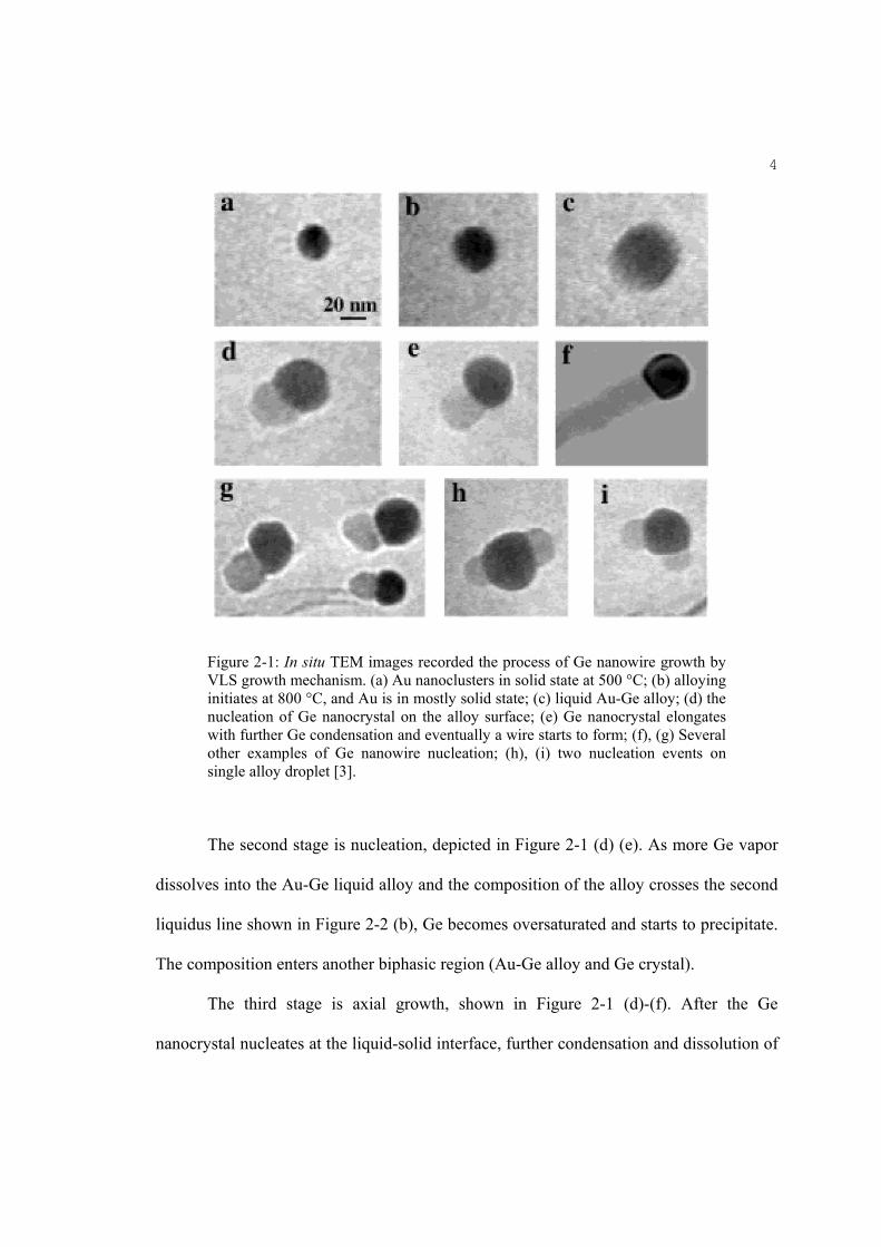
Figure 2-1 is a TEM image taken by Yiying Wu and Peidong Yang [3] showing
three stages of nanowire growth by VLS growth mechanism. VLS growth of nanowires
typically uses metal nanoparticles, for example Au or Fe, as the catalyst, and these seed
particles initiate nanowire growth. In Wu and Yang’s experiment, Au was used as the
catalyst, and the sample stage was maintained at 800 - 900 °C.
The first stage in VLS nanowire growth is called alloying. In this stage, chemical
reactions take place between seed particles and the vapor of the target nanowire’s
chemical elements. This stage is illustrated in Figure 2-1 (a)-(c). The Au nanoclusters
react with Ge vapor and form Au-Ge liquid alloy. In Figure 2-2, this stage is also
represented by an isothermal line on the Au-Ge phase diagram.
4
Figure 2-1: In situ TEM images recorded the process of Ge nanowire growth by VLS growth mechanism. (a) Au nanoclusters in solid state at 500 °C; (b) alloying initiates at 800 °C, and Au is in mostly solid state; (c) liquid Au-Ge alloy; (d) the nucleation of Ge nanocrystal on the alloy surface; (e) Ge nanocrystal elongates with further Ge condensation and eventually a wire starts to form; (f), (g) Several other examples of Ge nanowire nucleation; (h), (i) two nucleation events on single alloy droplet [3].
The second stage is nucleation, depicted in Figure 2-1 (d) (e). As more Ge vapor
dissolves into the Au-Ge liquid alloy and the composition of the alloy crosses the second
liquidus line shown in Figure 2-2 (b), Ge becomes oversaturated and starts to precipitate.
The composition enters another biphasic region (Au-Ge alloy and Ge crystal).
The third stage is axial growth, shown in Figure 2-1 (d)-(f). After the Ge
nanocrystal nucleates at the liquid-solid interface, further condensation and dissolution of

5
Ge vapor into the Au-Ge liquid alloy increases the amount of Ge crystal precipitation
from the alloy. Because less energy is needed with crystal step growth compared to
secondary nucleation events in a finite volume [3], Ge will prefer to diffuse and condense
at the existing liquid-solid interface and therefore form a nanowire. This is illustrated as a
cartoon in Figure 2-2 (a) II III.
Figure 2-2: Three stages in VLS nanowire growth mechanism shown in (a) a schematic illustration; (b) conventional Au-Ge binary phase diagram [3].
The Si1-xGex and GaP nanowires studied in this thesis were all grown by the VLS
growth mechanism and I will discuss the detailed growth methods for each of them.
6
2.2 Chemical Vapor Deposition (CVD) Growth Method for Si1-xGex Nanowires
The growth procedure of Si1-xGex nanowires follows the method described in Ref.
[4]. Commercial anodic alumina membranes with nominal 200 nm diameter pores were
used as a platform. A 5 micron long segment of Ag was deposited in the pores, and
afterwards, a 0.25 micron long Au segment was deposited in those pores. The Ag
segment was removed by etching in 8.0M HNO3 so that only the thin Au segment near
the top of the membrane was left to serve as the catalyst.
However, because of low growth rate of Si1-xGex nanowires with x greater than
0.8, those nanowires were grown on Si(111) substrate coated with a 200 nm thick Au
film instead of on the anodic alumina membranes.
Figure 2-3 illustrates the CVD setup of Si1-xGex nanowire growth. The alumina
membranes or the Si(111) substrates were placed at the center of an isothermal quartz
reactor tube. The growth temperature was maintained as a constant between 325 °C to
500 °C. Si1-xGex nanowires grown under different growth temperature have different Ge
concentration x.
SiH4 and GeH4 were used as gaseous precursor sources for the growth of Si1-xGex
nanowires growth. The total pressure within the quartz reactor was held constant at 13
Torr using 10% mixture of SiH4 in H2 and 1% or 2% GeH4 in H2. The total gas rate was
held constant as 100 sccm. The flow rate of each source gas was adjusted to control the
inlet gas ratio of GeH4 / (SiH4 + GeH4) from 0.01 to 0.67. The difference in the inlet gas
ratio also had influence over the Ge composition in Si1-xGex nanowires.
Figu
2.3 Pulsed
GaP
weight ratio
milled in a
press as illu
uni-axial p
became a d
2-4 (d). Th
growth met
2-4 (e), an
through the
and at a p
maintained
ure 2-3: Si1-xG
Laser Vap
P crystals w
o of 95% G
a ball miller
ustrated by
ressure at 5
deeply-pres
his tablet is
thod. The G
nd put into
e quartz rea
pressure ins
d to be 880-9
Gex nanowir
porization (
were first m
GaP to 5% A
r for severa
y the cartoon
5 metric ton
sed compac
called a tar
GaP-Au targ
a quartz re
actor tube a
side the tu
920 °C.
re growth by
(PLV) Grow
mixed with
Au. The mi
al hours. Th
ns in Figur
ns for half
ct cylindric
rget becaus
get was held
eactor tube
at 100 sccm
ube of 200
CVD.
wth Metho
h micron si
ixture was
he fine pow
e 2-4 (a)-(c
day. After
al tablet sim
se it is ablat
d by a target
at place “
m to carry th
torr. The
od for GaP
ize Au part
ground into
wders were
c) [5], and t
this treatm
milar as the
ted by a las
t holder, su
“A” in Figu
he GaP vap
temperatur
Nanowires
ticles (cata
o a powder
placed ins
this pellet w
ment, GaP-A
e one show
ser in subse
ch as the on
ure 2-5. Ar
por plume d
re of the fu
7
s
alyst) at the
and further
ide a pellet
was applied
Au powders
wn in Figure
equent PLV
ne in Figure
gon flowed
downstream
furnace was
7
e
r
t
d
s
e
V
e
d
m
s
Figupresprep
Figu
In F
along a zigz
tablet. The
green circle
ure 2-4: PLVss; (b) bottompared target t
ure 2-5: GaP
Figure 2-5,
zag path as
small gree
es are discre
V target prepm of a pellet taken out fro
Nanowire g
the lens wa
depicted in
en solid circ
ete in the fi
paration. schpress; (c) bam a pullet pr
growth by PL
as connected
n Figure 2-6
cle in Figur
igure, the ac
hematic illusarrel of a pelress; (e) targ
LV.
d to a comp
6, so that the
re 2-6 repre
ctual movem
tration of (allet press; picet holder [5]
puter-contro
e laser ablat
esents the l
ment of lase
a) top of a pcture of (d) f.
olled motor
ted evenly o
laser spot.
er spot was
8
pellet fresh
and moved
on the target
Though the
continuous
8
d
t
e
s

9
without any stop as indicated by the red lines. Odd runs and even runs were following
different directions for the purpose of even laser ablation.
Figure 2-6: Illustration of laser spot movement in PLV.
A narrow quartz collection tube was placed between position “B” and “M” in
Figure 2-5 to harvest GaP nanowires grown by this method.
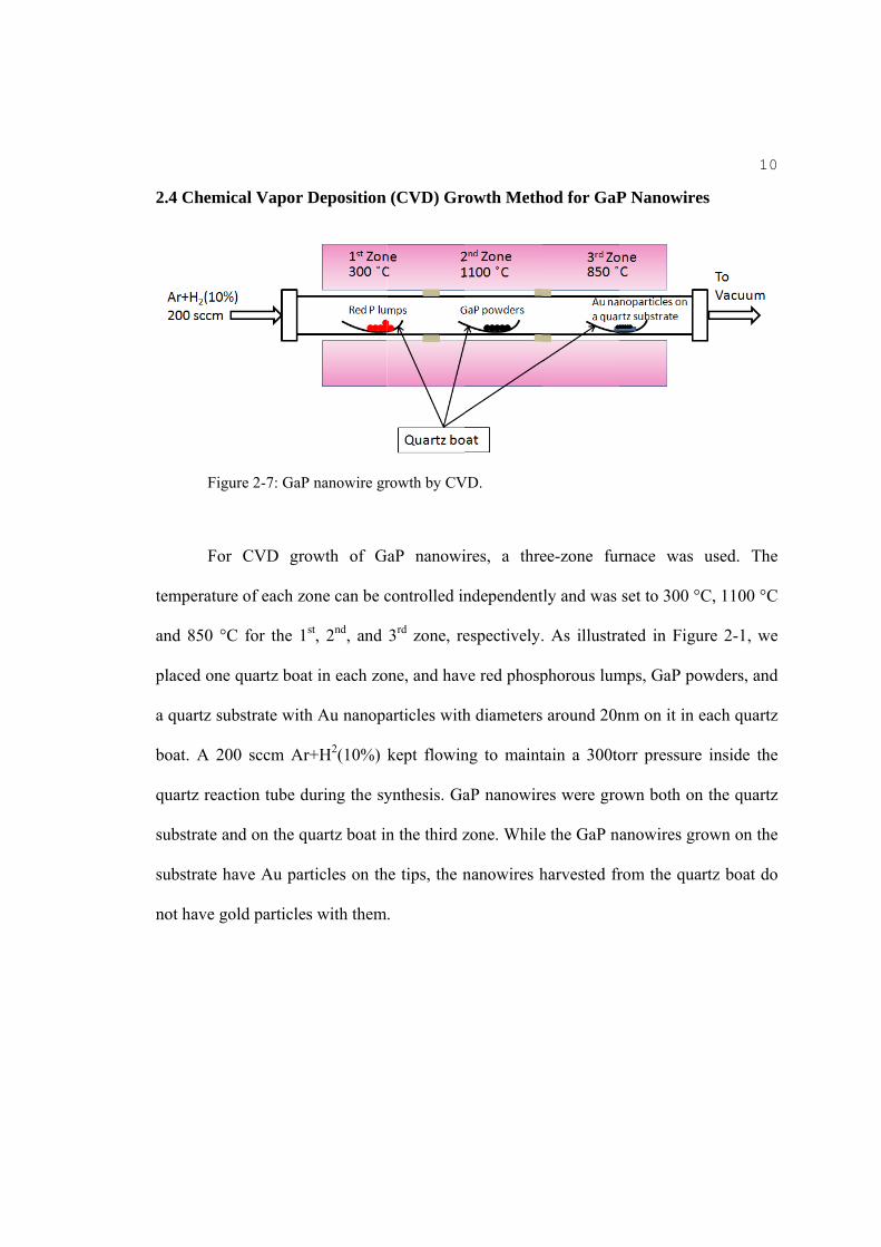
2.4 Chemic
Figu
For
temperature
and 850 °C
placed one
a quartz sub
boat. A 20
quartz reac
substrate an
substrate ha
not have go
cal Vapor D
ure 2-7: GaP
CVD gro
e of each zo
C for the 1s
quartz boat
bstrate with
00 sccm Ar+
ction tube du
nd on the qu
ave Au part
old particles
Deposition
nanowire gr
owth of G
one can be c
st, 2nd, and
t in each zo
h Au nanopa
+H2(10%)
uring the sy
uartz boat in
ticles on th
s with them
(CVD) Gr
rowth by CV
aP nanowi
controlled in
3rd zone, re
one, and hav
articles with
kept flowin
ynthesis. Ga
n the third z
he tips, the n
.
owth Meth
VD.
ires, a thre
ndependent
espectively.
ve red phosp
h diameters
ng to maint
aP nanowir
zone. While
nanowires h
hod for GaP
ee-zone fur
tly and was
. As illustra
phorous lum
around 20n
tain a 300to
es were gro
e the GaP n
harvested fr
P Nanowire
rnace was
set to 300 °
ated in Figu
mps, GaP po
nm on it in
orr pressure
own both on
anowires gr
rom the qua
10
es
used. The
°C, 1100 °C
ure 2-1, we
owders, and
each quartz
e inside the
n the quartz
rown on the
artz boat do
0
e
C
e
d
z
e
z
e
o
Chapter 3
Rayleigh and Raman Scattering
3.1 Introduction to Rayleigh and Raman Scattering
When monochromatic light is incident on systems smaller than its wavelength
such as nanowires, most of it will be scattered without change in frequency. This is called
“Rayleigh Scattering” after the English physicist Lard Rayleigh. However, a weaker part
of the scattering is inelastic and is called Raman scattering.
The scattering with change of frequency was predicted theoretically by Smekal in
1923 and was discovered by Sir C.V. Raman in February 1928. Raman was awarded the
Nobel Prize for Physics in 1930 for this discovery. The Raman effect is important in
several ways. The difference in wavenumber between the incident radiation and scattered
light carries with it information about the vibrational and rotational energy levels of the
molecules and atoms in a condensed matter system. This makes Raman spectroscopy a
powerful method to study energy level in such systems. Furthermore, in some cases,
certain lines or transitions may be entirely forbidden in the infrared spectroscopy by
selection rules. So Raman spectra are needed to provide us with the maximum
information about molecules and condensed matter systems.
12
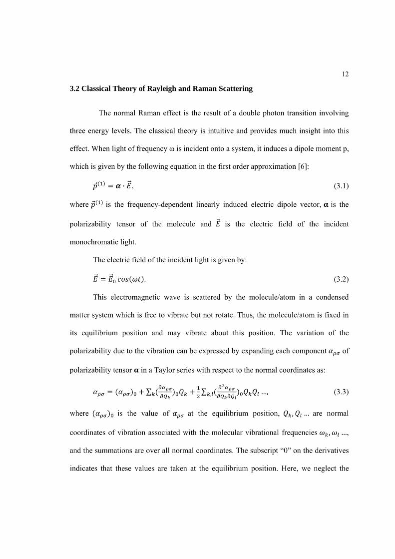
3.2 Classical Theory of Rayleigh and Raman Scattering
The normal Raman effect is the result of a double photon transition involving
three energy levels. The classical theory is intuitive and provides much insight into this
effect. When light of frequency ω is incident onto a system, it induces a dipole moment p,
which is given by the following equation in the first order approximation [6]:
· , (3.1)
where is the frequency-dependent linearly induced electric dipole vector, is the
polarizability tensor of the molecule and is the electric field of the incident
monochromatic light.
The electric field of the incident light is given by:
. (3.2)
This electromagnetic wave is scattered by the molecule/atom in a condensed
matter system which is free to vibrate but not rotate. Thus, the molecule/atom is fixed in
its equilibrium position and may vibrate about this position. The variation of the
polarizability due to the vibration can be expressed by expanding each component of
polarizability tensor in a Taylor series with respect to the normal coordinates as:
∑ ∑ …, , (3.3)
where is the value of at the equilibrium position, , … are normal
coordinates of vibration associated with the molecular vibrational frequencies , …,
and the summations are over all normal coordinates. The subscript “0” on the derivatives
indicates that these values are taken at the equilibrium position. Here, we neglect the
13
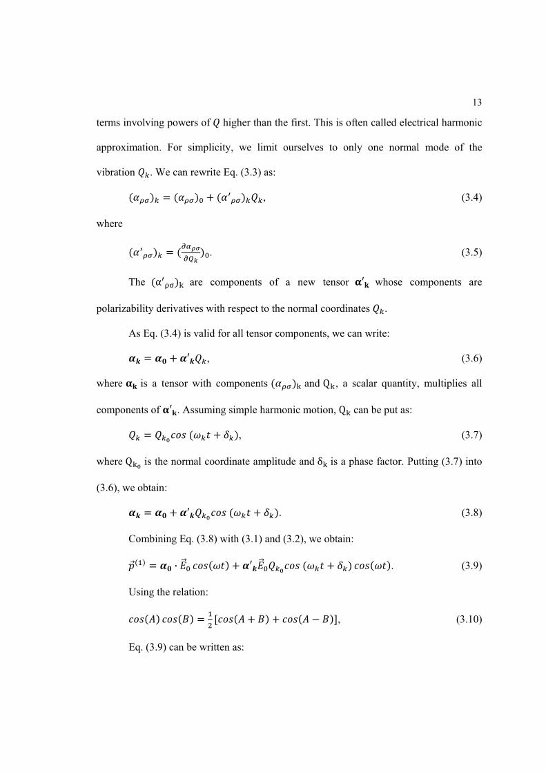
terms involving powers of higher than the first. This is often called electrical harmonic
approximation. For simplicity, we limit ourselves to only one normal mode of the
vibration . We can rewrite Eq. (3.3) as:
, (3.4)
where
. (3.5)
The α are components of a new tensor whose components are
polarizability derivatives with respect to the normal coordinates .
As Eq. (3.4) is valid for all tensor components, we can write:
, (3.6)
where is a tensor with components and Q , a scalar quantity, multiplies all
components of . Assuming simple harmonic motion, Q can be put as:
, (3.7)
where Q is the normal coordinate amplitude and δ is a phase factor. Putting (3.7) into
(3.6), we obtain:
. (3.8)
Combining Eq. (3.8) with (3.1) and (3.2), we obtain:
· . (3.9)
Using the relation:
, (3.10)
Eq. (3.9) can be written as:
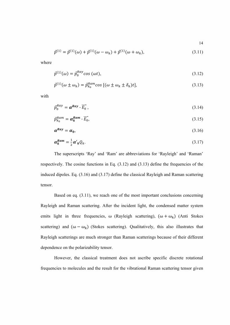
14
, (3.11)
where
, (3.12)
, (3.13)
with
· , (3.14)
· , (3.15)
, (3.16)
. (3.17)
The superscripts ‘Ray’ and ‘Ram’ are abbreviations for ‘Rayleigh’ and ‘Raman’
respectively. The cosine functions in Eq. (3.12) and (3.13) define the frequencies of the
induced dipoles. Eq. (3.16) and (3.17) define the classical Rayleigh and Raman scattering
tensor.
Based on eq. (3.11), we reach one of the most important conclusions concerning
Rayleigh and Raman scattering. After the incident light, the condensed matter system
emits light in three frequencies, ω (Rayleigh scattering), ω ω (Anti Stokes
scattering) and ω ω (Stokes scattering). Qualitatively, this also illustrates that
Rayleigh scatterings are much stronger than Raman scatterings because of their different
dependence on the polarizability tensor.
However, the classical treatment does not ascribe specific discrete rotational
frequencies to molecules and the result for the vibrational Raman scattering tensor given
15
by Eq. (3.17) is partly correct. We need to refer to the quantum theory for more detailed
understanding of Rayleigh and Raman scattering.
3.3 Quantum Theory of Rayleigh and Raman Scattering
Our treatment is based on time-dependent perturbation theory. The first-order
induced transition electric dipole moment is given by [6]:
| | , (3.18)
where and are the unperturbed time-dependent wave functions of the initial
state i and the final state f, and are the corresponding first-order perturbed time-
dependent wave functions, and is the electric dipole moment operator.
To evaluate Eq. (3.18), we make the following assumptions: the perturbation is
first order, the interaction Hamiltonian for the perturbation is entirely electric dipole in
nature and the perturbation is produced by the time-dependent electric field associated
with a plane monochromatic electromagnetic wave of frequency ω. Besides, due to the
complex nature of Eq. (3.18), we rewrite it as:
| | , (3.19)
and define the real induced transition electric dipole moment as
, (3.20)
where is the complex conjugate of . This definition in Eq. (3.20) follows
the way generally used in the literature and does not involve the factor 1/2.
16
Based on the assumptions we made, we can obtain the expression for the real
induced transition electric dipole moment as:
22 Γ
exp
Γ exp
22 Γ
exp
Γexp
.
(3.21)
The wave functions , , are time-dependent unperturbed wave functions of
the state i, j and r, respectively.
, (3.22)
where
. (3.23)
is the energy (unit: J) of the state r, and 2Γ (unit: rad/s) relates to the full width
of the level r. For the initial and final states i and f, we assume their lifetimes are infinite
so that 0. The double subscript on means a frequency difference such as:
. (3.24)
17
and are the and components of the electric dipole moment operator.
is the component of the complex amplitude of the incident plane wave with
frequency .
The terms in Eq. (3.21) contain two type of frequency dependence, namely
frequency of and frequency of . The terms involving
describe induced emission of two quanta, and , from an initial state which is
an excited level to a lower level . These will not be considered here.
If is negative, which means the energy of final state is lower than the initial
state, this is anti-Stokes Raman scattering. If is zero, the final state has the same
energy as the initial state and this is Rayleigh scattering. When is greater than zero,
the energy of final state is greater than the initial state, and this is Stokes Raman
scattering.
Here we write Stokes and anti-Stokes Raman part of the component of the real
induced transition electric dipole moment as:
22
,
.
(3.25)
We now introduce general transition polarizability with component
defined as:
18
2
,
.
(3.26)
Here | is the abbreviation for | , and so are | and | .
The energy of the state r, in principle, can lie above the initial and final state,
between the final and initial state, or below both final and initial states. However, we will
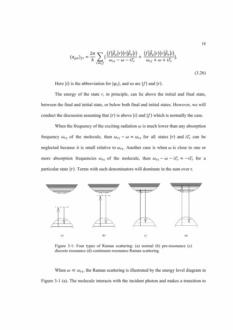
conduct the discussion assuming that | is above | and | which is normally the case.
When the frequency of the exciting radiation is much lower than any absorption
frequency of the molecule, then for all states | and can be
neglected because it is small relative to . Another case is when is close to one or
more absorption frequencies of the molecule, then for a
particular state | . Terms with such denominators will dominate in the sum over r.
Figure 3-1: Four types of Raman scattering: (a) normal (b) pre-resonance (c) discrete resonance (d) continuum resonance Raman scattering.
When , the Raman scattering is illustrated by the energy level diagram in
Figure 3-1 (a). The molecule interacts with the incident photon and makes a transition to
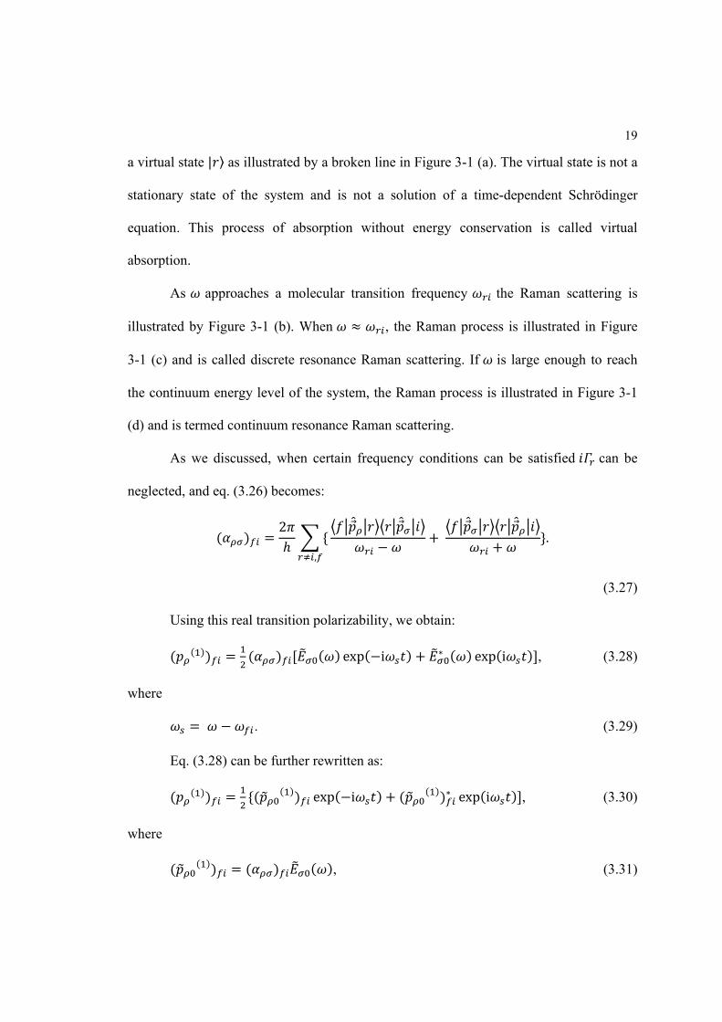
19
a virtual state | as illustrated by a broken line in Figure 3-1 (a). The virtual state is not a
stationary state of the system and is not a solution of a time-dependent Schrödinger
equation. This process of absorption without energy conservation is called virtual
absorption.
As approaches a molecular transition frequency the Raman scattering is
illustrated by Figure 3-1 (b). When , the Raman process is illustrated in Figure
3-1 (c) and is called discrete resonance Raman scattering. If is large enough to reach
the continuum energy level of the system, the Raman process is illustrated in Figure 3-1
(d) and is termed continuum resonance Raman scattering.
As we discussed, when certain frequency conditions can be satisfied can be
neglected, and eq. (3.26) becomes:
2
,
.
(3.27)
Using this real transition polarizability, we obtain:
exp i exp i , (3.28)
where
. (3.29)
Eq. (3.28) can be further rewritten as:
exp i exp i , (3.30)
where
, (3.31)
20
. (3.32)
When the electric field amplitude is real, , then
and eq. (3.30) becomes:
exp i exp i , (3.33)
where
. (3.34)
These results from quantum theory are similar to those obtained from classical
theory, but oscillating electric dipole and polarizability in classical theory are replaced
with transition electric dipole and polarizability. Besides, the transition polarizability is
defined in terms of the wave functions and energy levels of the system which make it
possible to associate the characteristics of scattering with the properties of the scattering
molecules as we discussed in Figure 3-1.
3.4 Raman Instrumentation
In this section, I will introduce the instrumentation on which the Raman and
Rayleigh measurements in this thesis were performed.
21
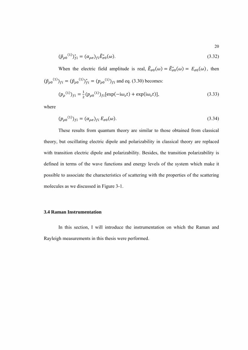
3.4.1 Horiba Jobin Yvon T64000 Raman System
Figure 3-2: a schematic diagram of Horiba Jobin Yvon T64000 spectrometer internal optics [7].
Figure 3-2 is an overall T64000 spectrometer functional diagram [7], and it shows
the optical path for macro- and micro-Raman as well as the different modes of
operations. These modes include: (1) single spectrograph; (2) double subtractive; (3)
triple additive mode. The single spectrograph mode uses only the third stage
monochromator and can get the highest optical throughput on weak scattering samples.
The double subtractive mode is used for the measurement of low frequency band close to
the laser line. Ultra high spectral resolution (<0.15cm-1) can be obtained by use of the
22
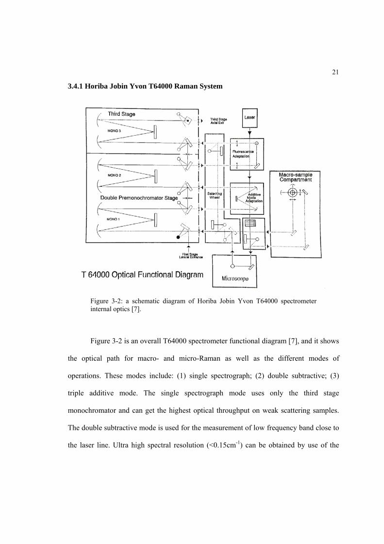
triple additive mode. The ray diagrams for double subtractive and triple additive mode
are illustrated in Figure 3-3.
Figure 3-3: optical diagram for (a) double subtractive (b) triple additive mode in Horiba Jobin Yvon T64000 spectrometer [7].
The single spectrograph mode in Horiba Jobin Yvon T64000 spectrometer was
used for the studying acoustic modes in Si1-xGex alloy nanowires (Chapter 4).
23
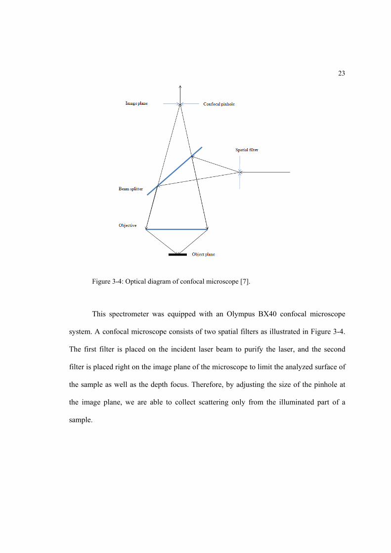
Figure 3-4: Optical diagram of confocal microscope [7].
This spectrometer was equipped with an Olympus BX40 confocal microscope
system. A confocal microscope consists of two spatial filters as illustrated in Figure 3-4.
The first filter is placed on the incident laser beam to purify the laser, and the second
filter is placed right on the image plane of the microscope to limit the analyzed surface of
the sample as well as the depth focus. Therefore, by adjusting the size of the pinhole at
the image plane, we are able to collect scattering only from the illuminated part of a
sample.
24
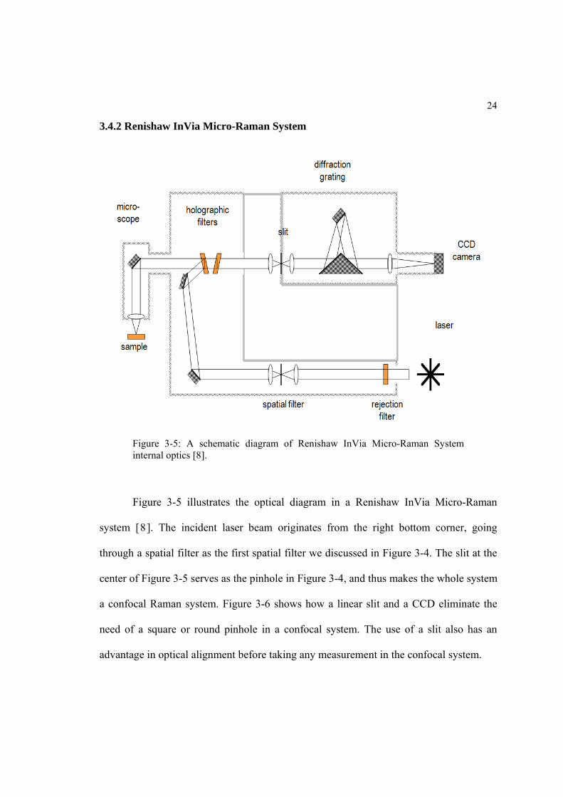
3.4.2 Renishaw InVia Micro-Raman System
Figure 3-5: A schematic diagram of Renishaw InVia Micro-Raman System internal optics [8].
Figure 3-5 illustrates the optical diagram in a Renishaw InVia Micro-Raman
system [8]. The incident laser beam originates from the right bottom corner, going
through a spatial filter as the first spatial filter we discussed in Figure 3-4. The slit at the
center of Figure 3-5 serves as the pinhole in Figure 3-4, and thus makes the whole system
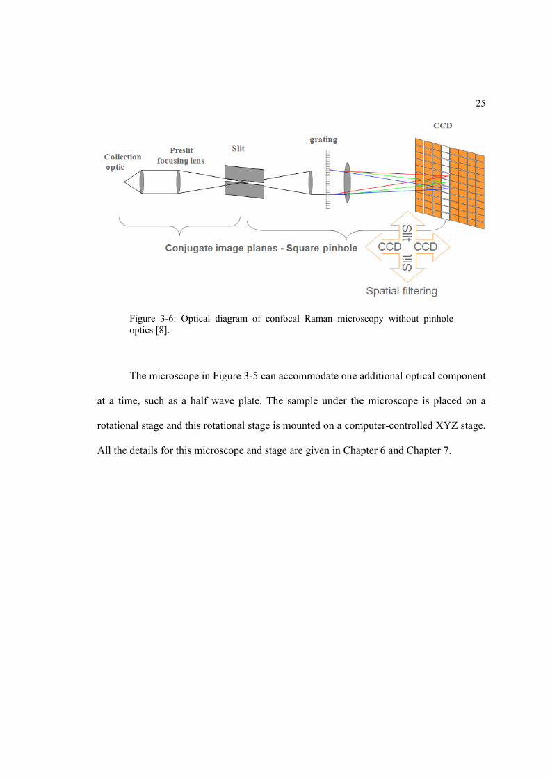
a confocal Raman system. Figure 3-6 shows how a linear slit and a CCD eliminate the
need of a square or round pinhole in a confocal system. The use of a slit also has an
advantage in optical alignment before taking any measurement in the confocal system.
25
Figure 3-6: Optical diagram of confocal Raman microscopy without pinhole optics [8].
The microscope in Figure 3-5 can accommodate one additional optical component
at a time, such as a half wave plate. The sample under the microscope is placed on a
rotational stage and this rotational stage is mounted on a computer-controlled XYZ stage.
All the details for this microscope and stage are given in Chapter 6 and Chapter 7.
Chapter 4
Raman Scattering from Si1-xGex Alloy Nanowires
4.1 Introduction
Semiconductor alloy nanowires have attracted increasing interest for bandgap
tunable electronic devices [9,10]. Si-Ge represents an example of such a system, even
though it has an indirect bandgap. Studies of Si1-xGex bulk material over the range 0≤x≤1
reveal continuous bandgap tunability from 0.7eV to 1.1eV [11] and they may provide an
opportunity for nanoscale electronic and optoelectronic devices. This binary system is
also suitable for optical fiber communication [12,13].
Electrical transport in nanowires is influenced by phonon scattering and Raman
scattering provides an important probe of the phonon properties of Si1-xGex nanowires
and their crystalline quality. The phonon properties of bulk Si and Ge [14], SiGe mixed
crystals [15,16], Si/Ge superlattices [17,18] and Si1-xGex nanoparticles [19,20] and films
[20] have been studied via Raman scattering [21,22,23]. To the best of our knowledge, no
Raman results had been reported on Si1-xGex alloy nanowires when this work was
published in 2008.
Here, I discuss the results of such studies on Si1-xGex alloy nanowires and our
experimental results will be compared to recent theoretical calculations [19] and
previously published results for crystalline bulk Si1-xGex samples and thin films [20].

27
4.2 Experimental Details
Si1-xGex NWs were grown by the VLS mechanism using CVD as discussed in
Chapter 2.2. Scanning electron microscopy (SEM, Philips XL20) was used for plan-view
imaging of the Si1-xGex nanowires showing the length of the nanowires in the range of 15
- 40 microns. Structural and chemical characterization of the NWs were carried out using
a JEOL 2010F field-emission TEM/STEM equipped with an X-ray energy dispersive
spectroscopy (EDS) system for elemental analysis. Chemical compositions of Si1-xGex
nanowires were quantified from the EDS data by the ζ method [24]. The ζ factor,
absorption corrections, and K-factors of Si and Ge Kα lines were calibrated using a
standard SiGe thin film sample. The minimum detectable limit of Ge in Si was measured
to be 0.8 at.%. For TEM characterization, Si1-xGex nanowires were released from the
substrate surface by sonication and then suspended in semiconductor-grade isopropanol.
A drop of the nanowire suspension was then placed onto a lacey carbon coated copper
grid for TEM observation.
Figure 4-1 (a) shows a low-magnification bright-field TEM image of the Si1-xGex
nanowires. The Au nanoparticle responsible for the VLS growth can be observed with
darker contrast at the tip of the wires. The crystalline growth direction of the nanowires
was mostly <111>. Inset in Figure 4-1 (a) shows the selected area electron diffraction
(SAD) pattern from an individual nanowire, this pattern is consistent with the reciprocal
lattice of the diamond structure observed along the [112] zone axis; the corresponding
nanowire growth direction (white arrow) is also indicated. Nevertheless, other growth
directions were also found, as shown in the inset of Figure 4-1 (b). The HRTEM image in

28
Figure 4-1 (b) shows the crystalline nature of these nanowires; the lattice fringes
corresponding to the [111] crystalline direction can be easily observed. A uniform
amorphous oxide coating of about 3 nm thick was typically observed on the outer surface
of the Si1-xGex nanowires. The Ge concentration in the outer oxide layer was very small;
i.e., the layer was found to be essentially silicon oxide by EDS. Many TEM images
similar to Figure 4-1 (a) were used to estimate the diameter distribution of these
nanowires. Typical nanowires exhibit a reasonably uniform diameter along the entire
length, i.e., without tapering. We could also observe a small modulation in the nanowire
diameter along the length, as we have reported in other VLS nanowire systems [25,26].
This modulation was not studied here. However, in polar semiconductors, e.g., GaP,
ZnO, etc., the modulation has been proposed to activate Raman scattering from surface
optic (SO) modes that lie between the transverse optic (TO) and longitudinal optic (LO)
modes.
Figure 4-1: (a) Low magnification bright-field TEM image of the Si1-xGex nanowires, the inset shows a SAD pattern from an individual nanowire with growth direction along the [111]. (b) High-resolution TEM image showing the crystalline nature of the Si1-xGex nanowires, the inset is the corresponding Fourier Transform and the white arrow indicates the growth direction ([131]) of this particular nanowire. Most nanowires were observed to grow in the [111] direction.
29
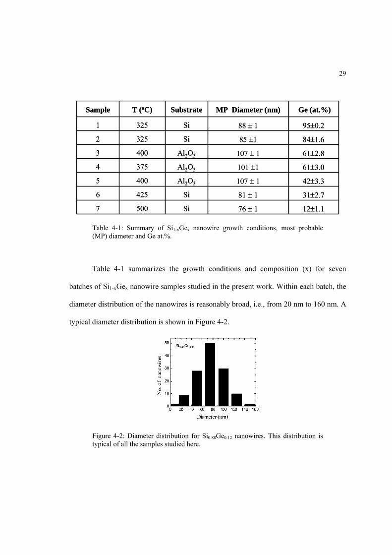
Table 4-1: Summary of Si1-xGex nanowire growth conditions, most probable (MP) diameter and Ge at.%.
Table 4-1 summarizes the growth conditions and composition (x) for seven
batches of Si1-xGex nanowire samples studied in the present work. Within each batch, the
diameter distribution of the nanowires is reasonably broad, i.e., from 20 nm to 160 nm. A
typical diameter distribution is shown in Figure 4-2.
Figure 4-2: Diameter distribution for Si0.88Ge0.12 nanowires. This distribution is typical of all the samples studied here.
Sample T (oC) Substrate MP Diameter (nm) Ge (at.%)
1 325 Si 88 ± 1 95±0.2
2 325 Si 85 ±1 84±1.6
3 400 Al2O3 107 ± 1 61±2.8
4 375 Al2O3 101 ±1 61±3.0
5 400 Al2O3 107 ± 1 42±3.3
6 425 Si 81 ± 1 31±2.7
7 500 Si 76 ± 1 12±1.1
Sample T (oC) Substrate MP Diameter (nm) Ge (at.%)
1 325 Si 88 ± 1 95±0.2
2 325 Si 85 ±1 84±1.6
3 400 Al2O3 107 ± 1 61±2.8
4 375 Al2O3 101 ±1 61±3.0
5 400 Al2O3 107 ± 1 42±3.3
6 425 Si 81 ± 1 31±2.7
7 500 Si 76 ± 1 12±1.1
30
The compositional homogeneity along the length of our nanowires was studied by
EDS. The Si/Ge ratio was found to be homogeneous along the nanowire to better than
1at.%. It was found that smaller diameter nanowires from the same batch showed a small
decrease of the Ge concentration (e.g. when d<50nm) [27]. For each batch, we averaged
the Ge concentration in 10 nanowires, all of which had a diameter very near to the most
probable diameter (~90-100nm) of the batch (c.f. Table 4-1).
4.3 Results and Discussions
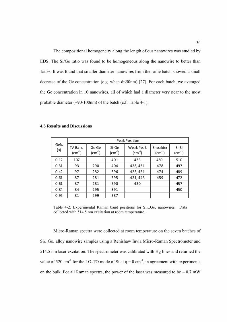
Table 4-2: Experimental Raman band positions for Si1-xGex nanowires. Data collected with 514.5 nm excitation at room temperature.
Micro-Raman spectra were collected at room temperature on the seven batches of
Si1-xGex alloy nanowire samples using a Renishaw Invia Micro-Raman Spectrometer and
514.5 nm laser excitation. The spectrometer was calibrated with Hg lines and returned the
value of 520 cm-1 for the LO-TO mode of Si at q = 0 cm-1, in agreement with experiments
on the bulk. For all Raman spectra, the power of the laser was measured to be ~ 0.7 mW
Ge% (x)
Peak Position
TA Band (cm‐1)
Ge‐Ge (cm‐1)
Si‐Ge (cm‐1)
Weak Peak (cm‐1)
Shoulder (cm‐1)
Si‐Si (cm‐1)
0.12 107 401 433 489 510
0.31 93 290 404 428, 451 478 497
0.42 97 282 396 423, 451 474 489
0.61 87 281 395 421, 443 459 472
0.61 87 281 390 430 457
0.84 84 295 391 450
0.95 81 299 387

31
with a hand-held radiometer at the sample. The nanowires were studied on the growth
substrate. Hundreds of nanowires were estimated to be illuminated within the 1 µm spot
size created by the objective lens (100x). In Si nanowires, it has been shown that phonon
confinement distortion of the otherwise Lorentzian LO-TO Raman band occurs for d ≤ 10
nm [28]. The present SiGe nanowires are too large in diameter (20 ≤ d ≤ 100 nm) to
exhibit phonon confinement. Although the spectra were collected under identical optical
conditions, the absolute intensity scales for each spectrum shown in Figure 4-3 through
Figure 4-6 should not be compared, since different numbers of wires were sampled in
each spectrum.
In Figure 4-3 we show the Raman spectra collected for the seven SixGe1-x
nanowire samples summarized in Table 4-1. The nanowires were dense enough on the
substrate that the Raman spectra do not exhibit the sharp band at 520 cm-1 from the
underlying Si (111) substrate. Each Raman spectrum is therefore the collective response
of many nanowires, representing the average x listed in Table 4-1. Three prominent
Raman bands can be observed in the figure whose intensity and position depend on x.
The lowest frequency band is located near ~300 cm-1 and is close in frequency to the q =
0 LO-TO phonon mode in pure Ge. It is therefore called the Ge-Ge band in the literature
(q is the wavevector of the phonon; the Raman selection rule in periodic systems requires
that only q = 0 phonons are observed). The highest frequency band in Figure 4-3 occurs
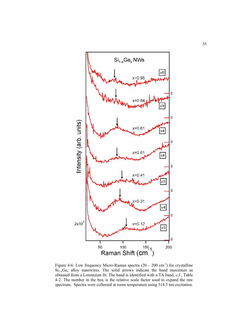
near 500 cm-1 and is close in frequency to the q = 0 LO-TO phonon mode in pure Si.
Therefore, it is called the Si-Si band. The Raman band in the middle of the spectrum ~
400 cm-1 is called the Si-Ge band. Theory has shown that the ~ 400 cm-1 band is a local
mode resulting from the vibration of Si atoms surrounded by 2 or more Ge atoms [19].

32
Figure 4-3: Micro-Raman spectra from seven batches of crystalline Si1-xGex alloy nanowires collected at room temperature with 514.5 nm excitation. The spectra were collected from wires remaining on the growth substrate and contain contributions from ~ 100 nanowires with random orientation relative to the incident polarization. Three prominent bands are observed and are referred to in the text and Table 4-2 as: (1) the Ge-Ge band (~ 300 cm-1); (2) the Si-Ge band (~ 400 cm-1); and (3) the Si-Si band (~ 500 cm-1). The dashed vertical lines refer to the position of the q = 0 LO-TO Raman band in pure crystalline Ge and Si.
33
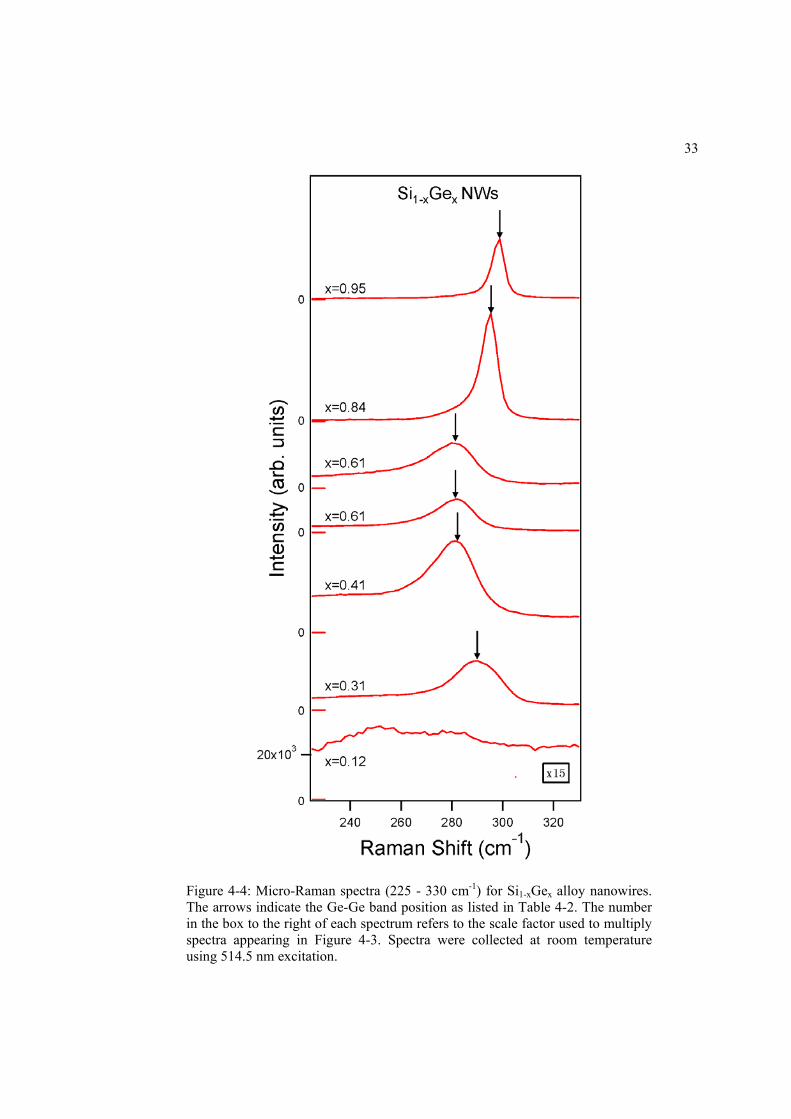
Figure 4-4: Micro-Raman spectra (225 - 330 cm-1) for Si1-xGex alloy nanowires. The arrows indicate the Ge-Ge band position as listed in Table 4-2. The number in the box to the right of each spectrum refers to the scale factor used to multiply spectra appearing in Figure 4-3. Spectra were collected at room temperature using 514.5 nm excitation.
34
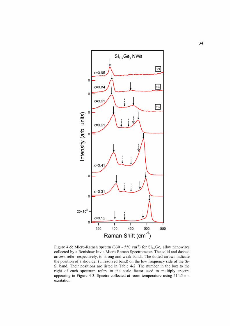
Figure 4-5: Micro-Raman spectra (330 - 550 cm-1) for Si1-xGex alloy nanowires collected by a Renishaw Invia Micro-Raman Spectrometer. The solid and dashed arrows refer, respectively, to strong and weak bands. The dotted arrows indicate the position of a shoulder (unresolved band) on the low frequency side of the Si-Si band. Their positions are listed in Table 4-2. The number in the box to the right of each spectrum refers to the scale factor used to multiply spectra appearing in Figure 4-3. Spectra collected at room temperature using 514.5 nm excitation.
35
Figure 4-6: Low frequency Micro-Raman spectra (20 – 200 cm-1) for crystalline Si1-xGex alloy nanowires. The solid arrows indicate the band maximum as obtained from a Lorentzian fit. The band is identified with a TA band, c.f., Table 4-2. The number in the box is the relative scale factor used to expand the raw spectrum. Spectra were collected at room temperature using 514.5 nm excitation.

36
Figure 4-3 shows that the Si-Si band position is the most sensitive to the Ge
concentration (x) and downshifts rapidly with increasing x. The peak position can
therefore be valuable for estimating x by Raman scattering. The behavior of the Ge-Ge
band, on the other hand, is a little more complicated. For clarity, we divide the spectra in
Figure 4-3 into low and high frequency regions: 225 - 330 cm-1 (Figure 4-4) and 330 –
550 cm-1 (Figure 4-5). As shown in Figure 4-4, the Ge-Ge band first downshifts slightly
with increasing x to its lowest frequency where the ratio Si/Ge ~ 1, and then upshifts.
This behavior is more evident in a plot of the Ge-Ge band position vs. x, as discussed
below. Figure 4-5 reveals more details about Raman spectra in the high frequency (330 –
550 cm-1) region. It shows that in addition to the Si-Ge and Si-Si band, there are one or
two weak features between 420 – 455 cm-1 and also a shoulder at the low frequency side
of the Si-Si band. The weak peaks (dashed arrows) appear for x = 0.12 ~ 0.61 and
become harder to resolve for x ≥ 0.84. The shoulder (dotted arrows) to the low frequency
side of the Si-Si band can be recognized for x = 0.12 ~ 0.61. The nanowire Raman peak
features will be compared to their counterparts in SiGe alloy bulk and liquid-phase-
epitaxy (LPE) films.
The structure in the Raman spectra for Si1-xGex shown in Figure 4-3 is strongly
correlated with the calculated vibrational density of states (VDOS) by Yu and co-workers
[19]. In Figure 4-7 we show their theoretical VDOS for crystalline Si1-xGex nanoparticles.
They used a valence force field model for a nearly spherical particle containing 1147
atoms (~ 3.5 nm) and the “mass-difference-only” approximation for the lattice dynamics.
In the mass-difference-only model, a universal set of stretching and bending force
constants are used for Si-Si, Ge-Ge and Si-Ge bonds to calculate the normal vibrational
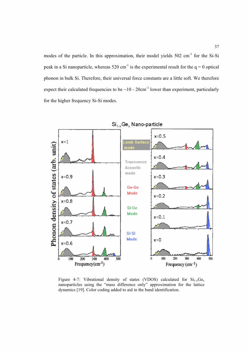
37
modes of the particle. In this approximation, their model yields 502 cm-1 for the Si-Si
peak in a Si nanoparticle, whereas 520 cm-1 is the experimental result for the q = 0 optical
phonon in bulk Si. Therefore, their universal force constants are a little soft. We therefore
expect their calculated frequencies to be ~10 - 20cm-1 lower than experiment, particularly
for the higher frequency Si-Si modes.
Figure 4-7: Vibrational density of states (VDOS) calculated for Si1-xGex nanoparticles using the “mass difference only” approximation for the lattice dynamics [19]. Color coding added to aid in the band identification.
38
As indicated schematically by the color code in Figure 4-7 for their calculated
VDOS, they find a broad VDOS band centered near ~ 75 – 100 cm-1 that they have
identified with nanoparticle modes analogous to the transverse acoustic (TA) modes in
the infinite solid. This TA VDOS band upshifts with decreasing x as the heavier Ge
atoms are replaced by the lighter Si atoms. The sharp peaks on the low frequency side of
the TA VDOS band are surface modes. Experimental difficulties (stray light rejection)
prevented us from collecting the Raman spectrum below ~ 100 cm-1 from the Renishaw
Invia Micro-Raman spectrometer. We therefore used a Jobin-Yvon T64000 Raman triple
grating spectrometer for spectra below 100 cm-1. The results are shown in Figure 4-6. The
TA band shows an overall trend to downshift as x increases. However, compared to the
calculated TA VDOS band, the experimental downshift (~ 30 cm-1) is lower than their
predicted value (~ 50 cm-1). The higher frequency theoretical VDOS bands associated
with the Ge-Ge, Si-Ge and Si-Si modes were easily observed by the Renishaw Invia
Micro-Raman Spectrometer. Figure 4-8 shows a detailed comparison between our Raman
spectrum for Si0.69Ge0.31 nanowires and the VDOS for Si0.7Ge0.3 nanoparticles calculated
by Yu and co-workers [19]. The agreement between our Raman spectra and the
calculated VDOS is very good. This suggests that the Raman scattering matrix element is
not a strong function of mode frequency. Recall that the theoretical calculation involves
only the VDOS and does not include the Raman matrix element. As we have discussed,
the force constants used in the calculations are slightly soft and we do observe a 20 – 30
cm-1 difference between theory and experiment for the highest frequency Si-Si band. It is
also noteworthy that several of the weaker calculated VDOS features, such as the small
peaks labeled (A, B) and a shoulder labeled C in Figure 4-8, are reproduced in our Raman
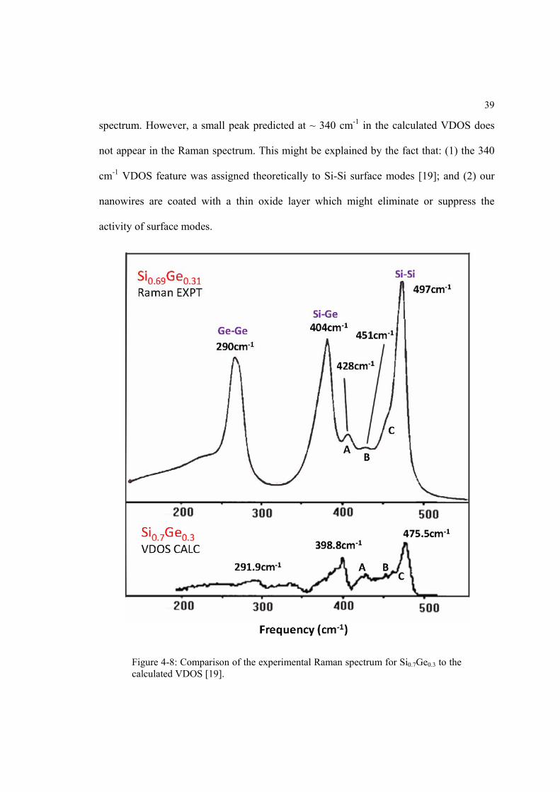
39
spectrum. However, a small peak predicted at ~ 340 cm-1 in the calculated VDOS does
not appear in the Raman spectrum. This might be explained by the fact that: (1) the 340
cm-1 VDOS feature was assigned theoretically to Si-Si surface modes [19]; and (2) our
nanowires are coated with a thin oxide layer which might eliminate or suppress the
activity of surface modes.
Figure 4-8: Comparison of the experimental Raman spectrum for Si0.7Ge0.3 to the calculated VDOS [19].
40
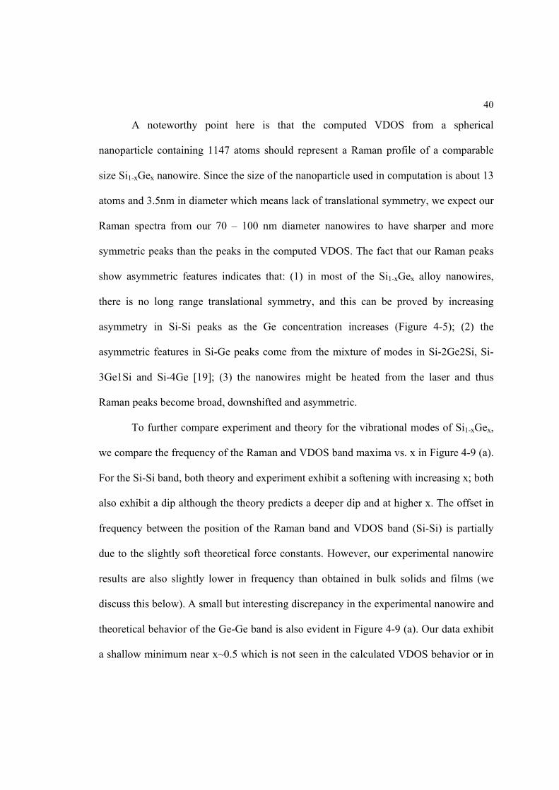
A noteworthy point here is that the computed VDOS from a spherical
nanoparticle containing 1147 atoms should represent a Raman profile of a comparable
size Si1-xGex nanowire. Since the size of the nanoparticle used in computation is about 13
atoms and 3.5nm in diameter which means lack of translational symmetry, we expect our
Raman spectra from our 70 – 100 nm diameter nanowires to have sharper and more
symmetric peaks than the peaks in the computed VDOS. The fact that our Raman peaks
show asymmetric features indicates that: (1) in most of the Si1-xGex alloy nanowires,
there is no long range translational symmetry, and this can be proved by increasing
asymmetry in Si-Si peaks as the Ge concentration increases (Figure 4-5); (2) the
asymmetric features in Si-Ge peaks come from the mixture of modes in Si-2Ge2Si, Si-
3Ge1Si and Si-4Ge [19]; (3) the nanowires might be heated from the laser and thus
Raman peaks become broad, downshifted and asymmetric.
To further compare experiment and theory for the vibrational modes of Si1-xGex,
we compare the frequency of the Raman and VDOS band maxima vs. x in Figure 4-9 (a).
For the Si-Si band, both theory and experiment exhibit a softening with increasing x; both
also exhibit a dip although the theory predicts a deeper dip and at higher x. The offset in
frequency between the position of the Raman band and VDOS band (Si-Si) is partially
due to the slightly soft theoretical force constants. However, our experimental nanowire
results are also slightly lower in frequency than obtained in bulk solids and films (we
discuss this below). A small but interesting discrepancy in the experimental nanowire and
theoretical behavior of the Ge-Ge band is also evident in Figure 4-9 (a). Our data exhibit
a shallow minimum near x~0.5 which is not seen in the calculated VDOS behavior or in
41
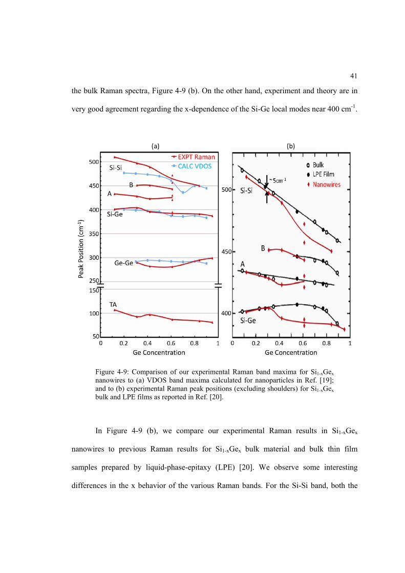
the bulk Raman spectra, Figure 4-9 (b). On the other hand, experiment and theory are in
very good agreement regarding the x-dependence of the Si-Ge local modes near 400 cm-1.
Figure 4-9: Comparison of our experimental Raman band maxima for Si1-xGex nanowires to (a) VDOS band maxima calculated for nanoparticles in Ref. [19]; and to (b) experimental Raman peak positions (excluding shoulders) for Si1-xGex bulk and LPE films as reported in Ref. [20].
In Figure 4-9 (b), we compare our experimental Raman results in Si1-xGex
nanowires to previous Raman results for Si1-xGex bulk material and bulk thin film
samples prepared by liquid-phase-epitaxy (LPE) [20]. We observe some interesting
differences in the x behavior of the various Raman bands. For the Si-Si band, both the
42
nanowire, the bulk and the LPE film samples exhibit an initial linear softening of the
band frequency with increasing x. Unlike the nanowires, the experimental bulk and LPE
film Si-Si band exhibits this linear behavior over the entire range of composition.
Furthermore, for x<0.5, the Si-Si band frequencies for the nanowires exhibit a rigid
downshift by ~5 cm-1 relative to the data for bulk and for LPE film samples. Since the
Ge-Ge, Si-Ge and Si-Si band position data from the bulk (open diamonds) and LPE films
(closed diamonds) are in such good agreement as shown in Figure 4-9 (b), it would
appear that the x behavior of the Raman bands for bulk Si-Ge alloys is fairly certain. We
will examine possible reasons for this downshift.
We can rule out the possibility of strain and phonon confinement. Oxide induced
compressive strain would be expected to upshift the band instead of downshifting it. Our
nanowires are large in diameter (~ 80 – 100 nm) and should exhibit bulk behavior.
Therefore, the difference in experimental nanowire and bulk results cannot be due to
phonon confinement effects. Elevated nanowire temperatures due to laser heating would
be expected to lower the band frequencies as the lattice undergoes thermal expansion.
However, the laser power we used here was about 0.7 mW at a 1 μm size spot, the typical
laser power we worked with for micro-Raman on nanowire bundles and single
nanowires. Though we did not carry out experiments under different laser powers to
definitely exclude the possibility of heating induced downshifting, our other experiments
of micro-Raman on single GaP nanowires with the same laser power did not show
significant peak shifting compared to other published Raman peak positions from GaP
nanoparticles [25, 29]. Therefore, heating should not be the main factor to downshift the
43
peak position so much as observed in the Si-Si peak, especially for nanowires with Ge
concentration (x) greater than 0.6.
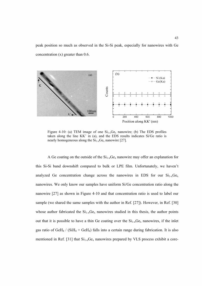
Figure 4-10: (a) TEM image of one Si1-xGex nanowire; (b) The EDS profiles taken along the line KK’ in (a), and the EDS results indicates Si/Ge ratio is nearly homogeneous along the Si1-xGex nanowire [27].
A Ge coating on the outside of the Si1-xGex nanowire may offer an explanation for
this Si-Si band downshift compared to bulk or LPE film. Unfortunately, we haven’t
analyzed Ge concentration change across the nanowires in EDS for our Si1-xGex
nanowires. We only know our samples have uniform Si/Ge concentration ratio along the
nanowire [27] as shown in Figure 4-10 and that concentration ratio is used to label our
sample (we shared the same samples with the author in Ref. [27]). However, in Ref. [30]
whose author fabricated the Si1-xGex nanowires studied in this thesis, the author points
out that it is possible to have a thin Ge coating over the Si1-xGex nanowires, if the inlet
gas ratio of GeH4 / (SiH4 + GeH4) falls into a certain range during fabrication. It is also
mentioned in Ref. [31] that Si1-xGex nanowires prepared by VLS process exhibit a core-
44
shell structure with a low Ge concentration in core and high Ge concentration in shell.
Here, I make the assumption that our Si1-xGex nanowires have a Ge-rich shell and a Si-
rich core.
Later in Chapter 6.4, I will present simulation results to support the conclusion
that for certain diameter of GaP nanowires, measured Raman intensities are dominated by
two regions of the nanowire. These two regions are both near the surface. As for the
simulation, Si1-xGex and GaP are only different in their dielectric constants. Therefore, we
expect the simulation results and conclusions from GaP to be suitable also for our Si1-
xGex nanowires. From this simulation result and the assumption of the Ge rich shell, we
conclude that our sample is mislabeled for Raman purpose. They should have been
labeled according to the Si/Ge ratio in the shell instead of the overall ratio, and these new
labels x would be greater than the existing labels. This currently underestimated labels x
leads to the Si-Si band’s left-shift. However, all these are based on assumptions, and
require our further investigation.
4.4 Conclusion
We have grown Si1-xGex nanowires by the CVD approach with gold particle using
gas mixtures of silane, germane and hydrogen. Nanowires with most probable diameter in
the range ~ 80-100 nm could be produced almost over the entire range 0<x<1. The
nanowires were found to have uniform Si to Ge ratio along their axis. The Raman spectra
of these Si1-xGex nanowires show three main bands (Si-Si, Si-Ge, Ge-Ge). The x
dependence of the prominent frequencies is in good agreement with the recent VDOS
45
calculations of SiGe nanoparticles by Ren, Cheng and Yu in Ref. [19]. We also observed
several weaker Raman features (e.g. peak A, B and shoulder C in Figure 4-8) also in
good agreement with their theoretical results. The Raman spectra strongly resemble the
calculated VDOS, indicating the Raman matrix element is a weak function of frequency.
As previously found in the bulk, the Si-Si peak in our nanowires is the most sensitive to
Ge concentration, exhibiting a linear downshift with increasing x for x ≤ 0.5. Raman
scattering can therefore be used to estimate the Ge concentration in single Si1-xGex
nanowire. The nanowire’s Raman bands appear downshifted by 5 ~ 15 cm-1 (depending
on x) relative to those observed previously in bulk Si1-xGex samples or LPE films. We
also find a slightly different x dependence for the strongest intensity band frequencies
than observed in bulk and LPE films. The reason for these small discrepancies between
bulk and nanowire SiGe is not yet clear.
Chapter 5
Computational Methods for E field Scattered by Single Nanowire
In this chapter, I will present three different methods to calculate the electric field
scattered by a single nanowire and the electric field distribution within that nanowire.
These computations are all based on the classical theory, with no quantum theory
involved. We start with Maxwell’s equations:
· , (5.1)
0, (5.2)
· 0, (5.3)
, (5.4)
where is the electric field, is the magnetic field, and are the free charge density
and current density, respectively. The definitions of and H are:
, (5.5)
. (5.6)
Eq. (5.1) - (5.6) are not sufficient, and we need the following relations:
, (5.7)
, (5.8)
, (5.9)
where is the conductivity, is the permeability, and is the electric susceptibility.
47
5.1 Mie Scattering from an Infinitely Long Cylinder
Mie theory is an analytical solution to Maxwell’s equations. It was first developed
by German physicist Gustav Mie, to study the scattering of electromagnetic wave by
spherical particles. The theory was later developed to analytically solve the scattering
problems by stratified spheres and infinite cylinders.
One of the limitations of Mie scattering is that it can only deal with an incident
plane wave, while in our experiments we use Gaussian wave excitations. I will follow the
symbols and derivations in Ref. [32].
We can easily write down a plane electromagnetic wave as:
· , (5.10)
· , (5.11)
and we are able to obtain the following:
0, (5.12)
0, (5.13)
where . In addition, and are not independent, they must satisfy:
, (5.14)
. (5.15)
Suppose that, given a scalar function and an arbitrary constant vector , we
construct a vector :
. (5.16)
This vector satisfies:
48
· 0, (5.17)
. (5.18)
Therefore, M satisfies the vector wave equation (5.12) if is a solution to the
scalar wave equation:
0. (5.19)
We may rewrite Eq. (5.16) as , which clearly shows is
perpendicular to vector . Now let us construct another vector:
M. (5.20)
This vector has zero divergence and satisfies the vector wave equation:
0 (5.21)
and
. (5.22)
Therefore, and have all the properties of an electromagnetic wave: they
satisfy vector wave equation, they are divergence free, curl of is proportional , and
curl of is proportional to .
To obtain the analytical results for scattering from an infinitely long cylinder as
depicted by Figure 5-1, we start with the scalar wave equation (5.19). In the following
derivations, we use subscripts “i”, “l”, and “s” for incident wave, E or H field inside
cylinder, and scattered wave respectively.
In a cylindrical polar coordinate system (Figure 5-2), Eq. (5.19) can be rewritten
as:
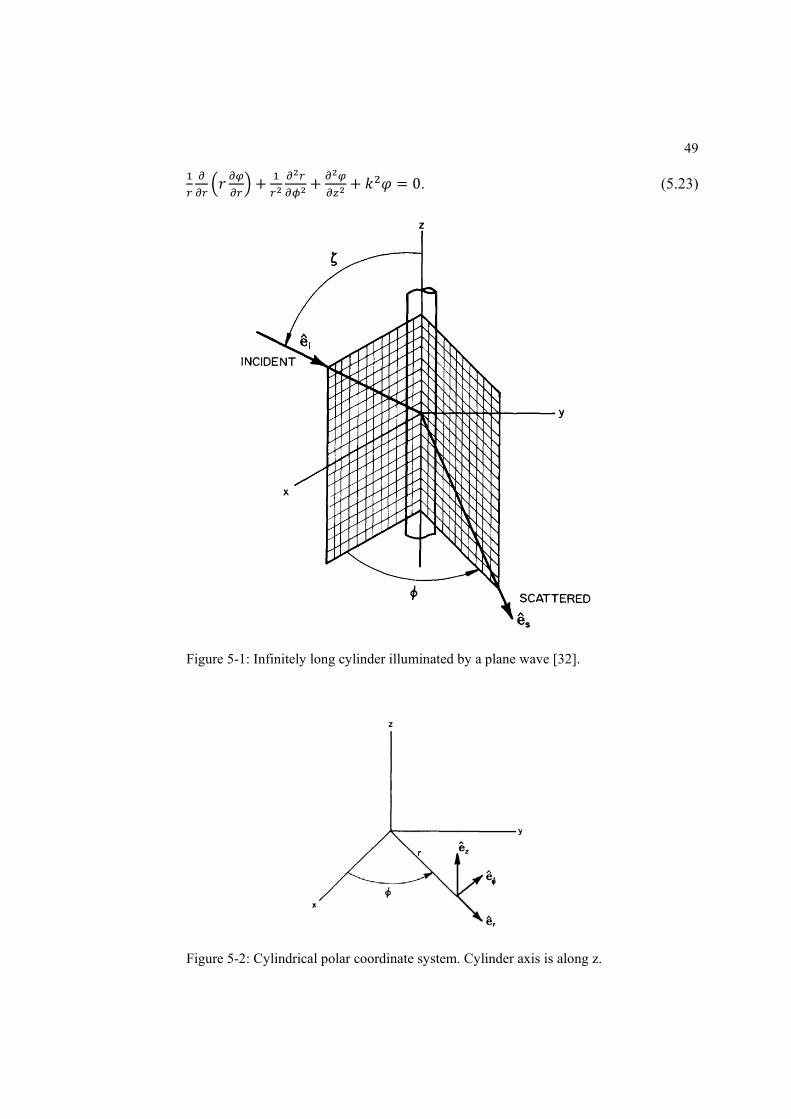
49
0. (5.23)
Figure 5-1: Infinitely long cylinder illuminated by a plane wave [32].
Figure 5-2: Cylindrical polar coordinate system. Cylinder axis is along z.
50
The solution to Eq. (5.23) takes the following form:
, , 0, 1,… , (5.24)
where √ and is a solution to the Bessel equation:
0. (5.25)
The linearly independent solutions to Eq. (5.25) are the Bessel functions of the
first and second kind, and with integer n. The constant is dictated by the form of
incident radiation and boundary conditions at the interface of the cylinder and
surrounding medium.
The vector cylindrical harmonics generated by Eq. (5.24) are:
√ , (5.26)
√ √ .
(5.27)
5.1.1 Incident Electric Field Parallel to the xz Plane
When the polarization of the incident light is parallel to the xz plane in Figure 5-1,
we can express the incident electric field:
(5.28)
in vector cylindrical harmonics as:
∑ . (5.29)
51
The superscript (1) in eq. (5.29) means we only use Bessel functions of the first
kind in order to have a finite value at 0. To determine the coefficients and , we
use the orthogonality of the vector harmonics, and can finally conclude:
0, (5.20)
. (5.21)
Therefore, we can write the incident electromagnetic field as:
∑ , (5.22)
∑ , (5.23)
where
. (5.24)
Next, we express the electromagnetic field in terms of Bessel functions of the first
kind due to the finiteness requirement at the origin:
∑ , (5.25)
∑ . (5.26)
The scattered electromagnetic field should be expressed in terms of Bessel
functions of the third kind, an outgoing wave:
∑ , (5.27)
∑ . (5.28)
If we apply the boundary conditions at , we can obtain the coefficients:
, (5.29)
52
, (5.30)
1 , (5.31)
1 , (5.32)
, (5.33)
, (5.34)
, (5.35)
where is refractive index of the cylinder relative to the surrounding medium, and
, (5.36)
, (5.37)
. (5.38)
When the incident light is perpendicular to the cylinder axis ( 90°):
0, (5.39)
, (5.40)
, (5.41)
0. (5.42)
5.1.2 Incident Electric Field Perpendicular to the xz Plane
In this case, the incident electric field is:
∑ . (5.43)
53
The scattered field can be written as:
∑ , (5.44)
, (5.45)
, (5.46)
where , , and are defined in the previous section, and
. (5.47)
When the incident light is perpendicular to the cylinder axis ( 90°):
, (5.48)
0, (5.49)
0, (5.50)
. (5.51)
5.1.3 Conclusion of Mie Scattering
By use of these equations, we are able to numerically calculate both the scattered
electromagnetic field (far field and near field) and the field inside the cylinder. Although
we have the summations from ∞ to ∞ in these equations, they converge very quickly
and we only need to sum from 15 to 15 in practice. These are all the
advantages of the Mie scattering. However, it also has two main disadvantages: (1) it
requires a plane wave incident; (2) it can only deal with spheres and infinite long
cylinders, while our real nanowires are finite cylinders.
54
5.2 Discrete Dipole Approximation (DDA) Method
5.2.1 Introduction to DDA method
The Discrete Dipole Approximation is a finite element method, first proposed by
Purcell and Pennypacker in 1973 to calculate scattering and absorption of
electromagnetic fields by irregular objects such as interstellar dust. In this method, the
continuum target is replaced with an array of discrete dipoles, or more precisely, discrete
polarizable points [33].
If we replace an arbitrary object by dipoles at position with polarizability
tensor , the polarization is:
· , (5.52)
where is the sum of incident plane wave
, exp · , (5.53)
and contributions from dipoles at other sites
, ∑ · . (5.54)
Here is the propagation vector in vacuum, , and are three-
dimensional vectors, and matrix is a array of 3 3 tensor.
Combining Eq. (5.52) – (5.54) together, we obtain:
· ∑ · , . (5.55)
Now the scattering problem for an array of point dipoles has become a system of
linear equations (5.55) and can be solved to arbitrary accuracy. The technique of Fast
55
Fourier Transform (FFT) can be applied to solve the system of linear equations with
10 [34].
Representing a continuum object with a array of dipoles requires us to specify (1)
the locations of each dipole ; and (2) the polarizability tensor of individual dipole .
We will need to first set up lattice grids and then determine the occupied grid sites. In the
simplest case, a cubic lattice, we want to represent our target by dipoles and suppose
that the volume of our target is . The lattice spacing can be determined as / .
The continuum target is characterized by its complex dielectric function and complex
refractive index / , in the limit of 0 , is the Clausius-Mossotti
polarizability [33]:
. (5.56)
But with a finite , the polarizability should include a radiative-reaction
correction [33]:
. (5.57)
5.2.2 Software for DDA Simulation in This Thesis
For the numerical study of electric field inside nanowire by implementation of
DDA method in this thesis, I obtain the results by use of shared DDA software,
“DDSCAT 6.1” coded by B. T. Draine in FORTRAN.
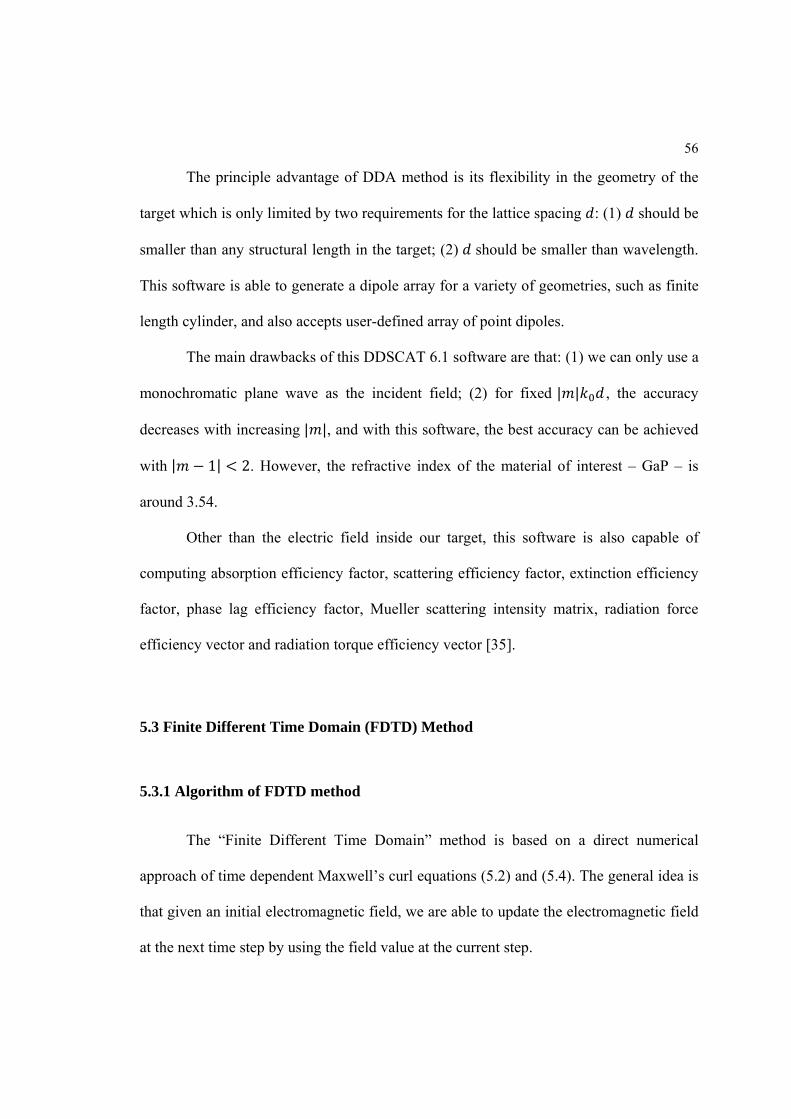
56
The principle advantage of DDA method is its flexibility in the geometry of the
target which is only limited by two requirements for the lattice spacing : (1) should be
smaller than any structural length in the target; (2) should be smaller than wavelength.
This software is able to generate a dipole array for a variety of geometries, such as finite
length cylinder, and also accepts user-defined array of point dipoles.
The main drawbacks of this DDSCAT 6.1 software are that: (1) we can only use a
monochromatic plane wave as the incident field; (2) for fixed | | , the accuracy
decreases with increasing | |, and with this software, the best accuracy can be achieved
with | 1| 2. However, the refractive index of the material of interest – GaP – is
around 3.54.
Other than the electric field inside our target, this software is also capable of
computing absorption efficiency factor, scattering efficiency factor, extinction efficiency
factor, phase lag efficiency factor, Mueller scattering intensity matrix, radiation force
efficiency vector and radiation torque efficiency vector [35].
5.3 Finite Different Time Domain (FDTD) Method
5.3.1 Algorithm of FDTD method
The “Finite Different Time Domain” method is based on a direct numerical
approach of time dependent Maxwell’s curl equations (5.2) and (5.4). The general idea is
that given an initial electromagnetic field, we are able to update the electromagnetic field
at the next time step by using the field value at the current step.
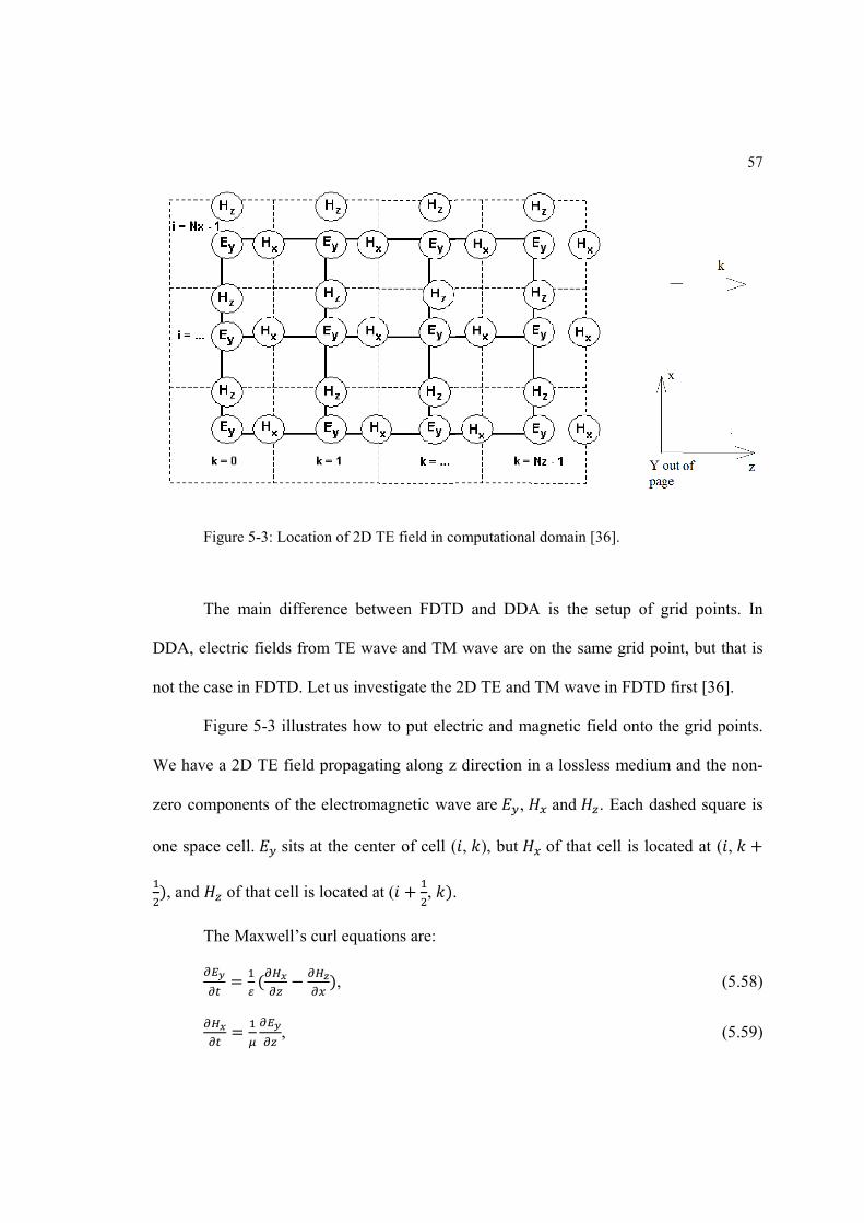
Figu
The
DDA, elect
not the case
Figu
We have a
zero compo
one space c
, and o
The
ure 5-3: Loca
e main diff
tric fields fr
e in FDTD.
ure 5-3 illu
2D TE fiel
onents of th
cell. sits
of that cell
e Maxwell’s
,
ation of 2D T
ference betw
from TE wa
Let us inve
ustrates how
ld propagati
he electrom
at the cent
is located a
s curl equati
,
TE field in co
ween FDTD
ave and TM
estigate the
w to put elec
ing along z
magnetic wav
ter of cell (
t ( , .
ions are:
omputationa
D and DDA
M wave are o
2D TE and
ctric and m
z direction i
ve are ,
( , ), but
l domain [36
A is the se
on the same
TM wave i
magnetic fiel
n a lossless
and .
of that ce
6].
etup of grid
e grid point
in FDTD fir
ld onto the
s medium a
Each dashe
ell is locate
57
d points. In
t, but that is
rst [36].
grid points
nd the non-
ed square is
ed at ( ,
(5.58)
(5.59)
7
n
s
.
-
s
)
)
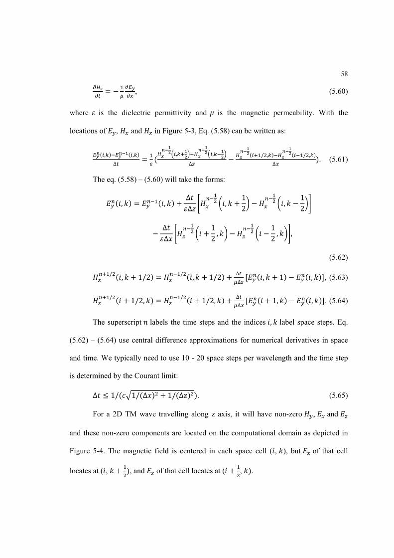
58
, (5.60)
where is the dielectric permittivity and is the magnetic permeability. With the
locations of , and in Figure 5-3, Eq. (5.58) can be written as:
, ,∆
, ,
∆/ , / ,
∆. (5.61)
The eq. (5.58) – (5.60) will take the forms:
, ,∆∆
,12
,12
∆∆
12 ,
12 , ,
(5.62)
/ , 1/2 / , 1/2 ∆∆
, 1 , , (5.63)
/ 1/2, / 1/2, ∆∆
1, , . (5.64)
The superscript labels the time steps and the indices , label space steps. Eq.
(5.62) – (5.64) use central difference approximations for numerical derivatives in space
and time. We typically need to use 10 - 20 space steps per wavelength and the time step
is determined by the Courant limit:
∆ 1/ 1/ ∆ 1/ ∆ . (5.65)
For a 2D TM wave travelling along z axis, it will have non-zero , and
and these non-zero components are located on the computational domain as depicted in
Figure 5-4. The magnetic field is centered in each space cell ( , ), but of that cell
locates at ( , , and of that cell locates at ( , .
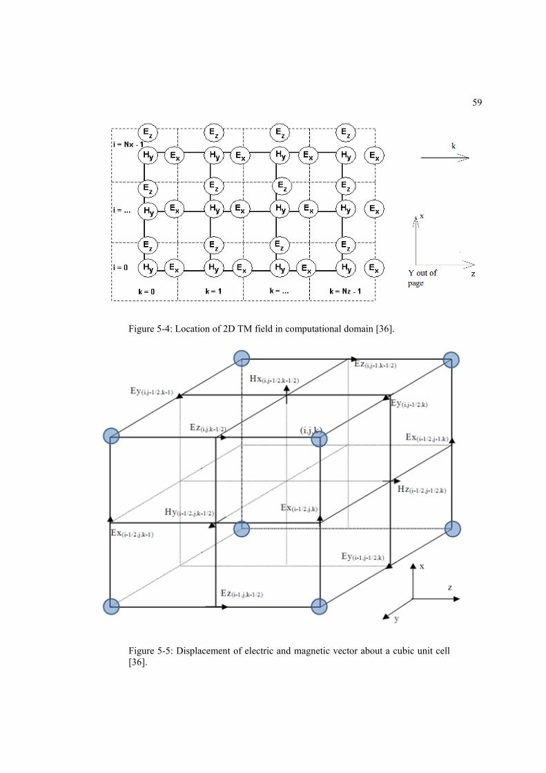
59
Figure 5-4: Location of 2D TM field in computational domain [36].
Figure 5-5: Displacement of electric and magnetic vector about a cubic unit cell [36].
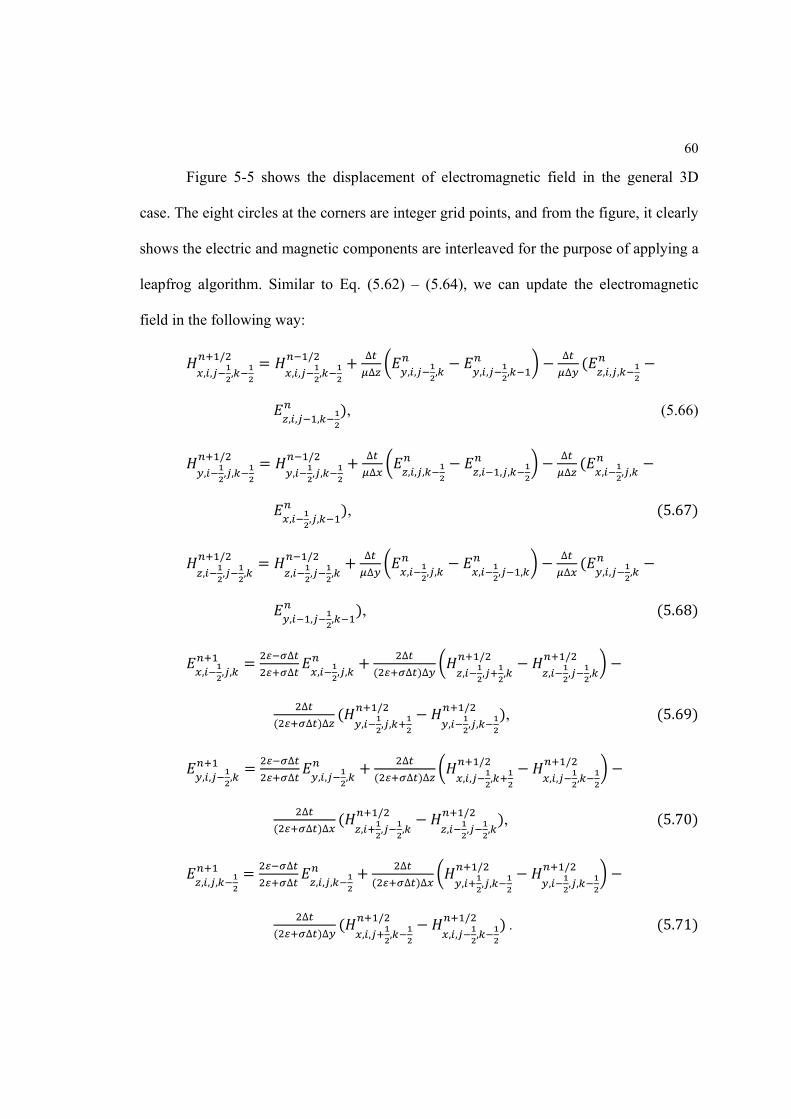
60
Figure 5-5 shows the displacement of electromagnetic field in the general 3D
case. The eight circles at the corners are integer grid points, and from the figure, it clearly
shows the electric and magnetic components are interleaved for the purpose of applying a
leapfrog algorithm. Similar to Eq. (5.62) – (5.64), we can update the electromagnetic
field in the following way:
, , ,/
, , ,/ ∆
∆ , , , , , ,∆∆ , , ,
, , ,, (5.66)
, , ,/
, , ,/ ∆
∆ , , , , , ,∆∆ , , ,
, , , , 5.67
, , ,/
, , ,/ ∆
∆ , , , , , ,∆∆ , , ,
, , , , 5.68
, , ,∆∆ , , ,
∆∆ ∆ , , ,
/, , ,
/
∆∆ ∆ , , ,
/, , ,
/ , 5.69
, , ,∆∆ , , ,
∆∆ ∆ , , ,
/, , ,
/
∆∆ ∆ , , ,
/, , ,
/ , 5.70
, , ,∆∆ , , ,
∆∆ ∆ , , ,
/, , ,
/
∆∆ ∆ , , ,
/, , ,
/ . 5.71
61
Similar to Eq. (5.65), the time step should satisfy the Courant-Friedrichs-Levy
condition:
∆ 1/ 1/ ∆ 1/ ∆ 1/ ∆ . (5.72)
The field propagated by the FDTD algorithm takes the form of:
, , , , . (5.73)
To obtain the complex field amplitude and phase information, Fourier transform
should be performed during the last time period of FDTD simulation.
5.3.2 Boundary Conditions in FDTD method
This FDTD algorithm must be modified at boundaries of the computational region
where suitable numerical absorbing boundary conditions (ABC) are applied. There are
several choices for the ABC, but the perfectly matched layer (PML) boundary conditions
have the best performance [36]. One version of the PML is called anisotropic PML, or
un-split PML (UPML). The implementation of the UPML boundary conditions is based
on Maxwellian formulation, and their absorbing properties are physically equivalent to
those of an absorbing uni-axial anisotropic medium with the following permittivity and
permeability tensors:
, , (5.74)
where
0 00 00 0
, . (5.75)
62
A plane wave incident on the above uni-axial medium will purely transmit into it.
This reflectionless propagation is independent on the angle of incident, polarization and
frequency of the wave. However, we need special treatment at the corner regions. For
example, the corner in a X-Z plane requires the tensor in Eq. (5.74) to be:
0 00 00 0
0 00 00 0
, , . (5.76)
5.3.3 Software for FDTD Method
The simulations by use of FDTD method were performed by Optiwave
OptiFDTD 8.0. The main advance in this FDTD software is its ability to use Gaussian
wave and a point light source as incident source. This means we are able to simulate the
electric field distributions inside a nanowire with laser profile as the incident wave.
Besides, we can also use the point light source as the oscillating dipole inside a nanowire
to investigate the efficiency of field emission from nanowire. The full picture of classical
Rayleigh and Raman scattering is the combination of the above two: (1) distribution of
electric field inside nanowire due to incident laser; (2) electric field emitted from
oscillating dipoles inside nanowire.
The main disadvantage of FDTD method is its long computational time and it is
not practical to calculate far-field emission.
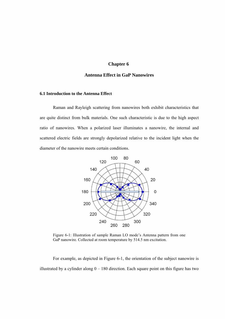
Chapter 6
Antenna Effect in GaP Nanowires
6.1 Introduction to the Antenna Effect
Raman and Rayleigh scattering from nanowires both exhibit characteristics that
are quite distinct from bulk materials. One such characteristic is due to the high aspect
ratio of nanowires. When a polarized laser illuminates a nanowire, the internal and
scattered electric fields are strongly depolarized relative to the incident light when the
diameter of the nanowire meets certain conditions.
Figure 6-1: Illustration of sample Raman LO mode’s Antenna pattern from one GaP nanowire. Collected at room temperature by 514.5 nm excitation.
For example, as depicted in Figure 6-1, the orientation of the subject nanowire is
illustrated by a cylinder along 0 – 180 direction. Each square point on this figure has two
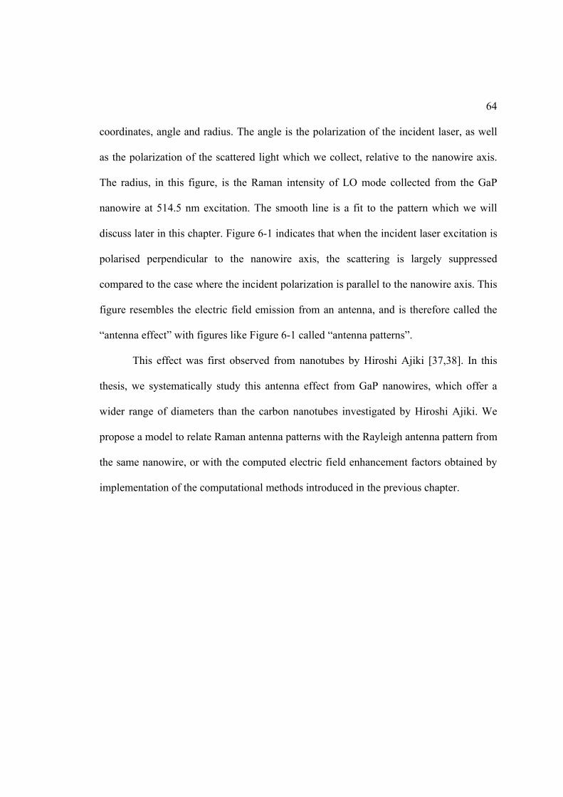
64
coordinates, angle and radius. The angle is the polarization of the incident laser, as well
as the polarization of the scattered light which we collect, relative to the nanowire axis.
The radius, in this figure, is the Raman intensity of LO mode collected from the GaP
nanowire at 514.5 nm excitation. The smooth line is a fit to the pattern which we will
discuss later in this chapter. Figure 6-1 indicates that when the incident laser excitation is
polarised perpendicular to the nanowire axis, the scattering is largely suppressed
compared to the case where the incident polarization is parallel to the nanowire axis. This
figure resembles the electric field emission from an antenna, and is therefore called the
“antenna effect” with figures like Figure 6-1 called “antenna patterns”.
This effect was first observed from nanotubes by Hiroshi Ajiki [37,38]. In this
thesis, we systematically study this antenna effect from GaP nanowires, which offer a
wider range of diameters than the carbon nanotubes investigated by Hiroshi Ajiki. We
propose a model to relate Raman antenna patterns with the Rayleigh antenna pattern from
the same nanowire, or with the computed electric field enhancement factors obtained by
implementation of the computational methods introduced in the previous chapter.
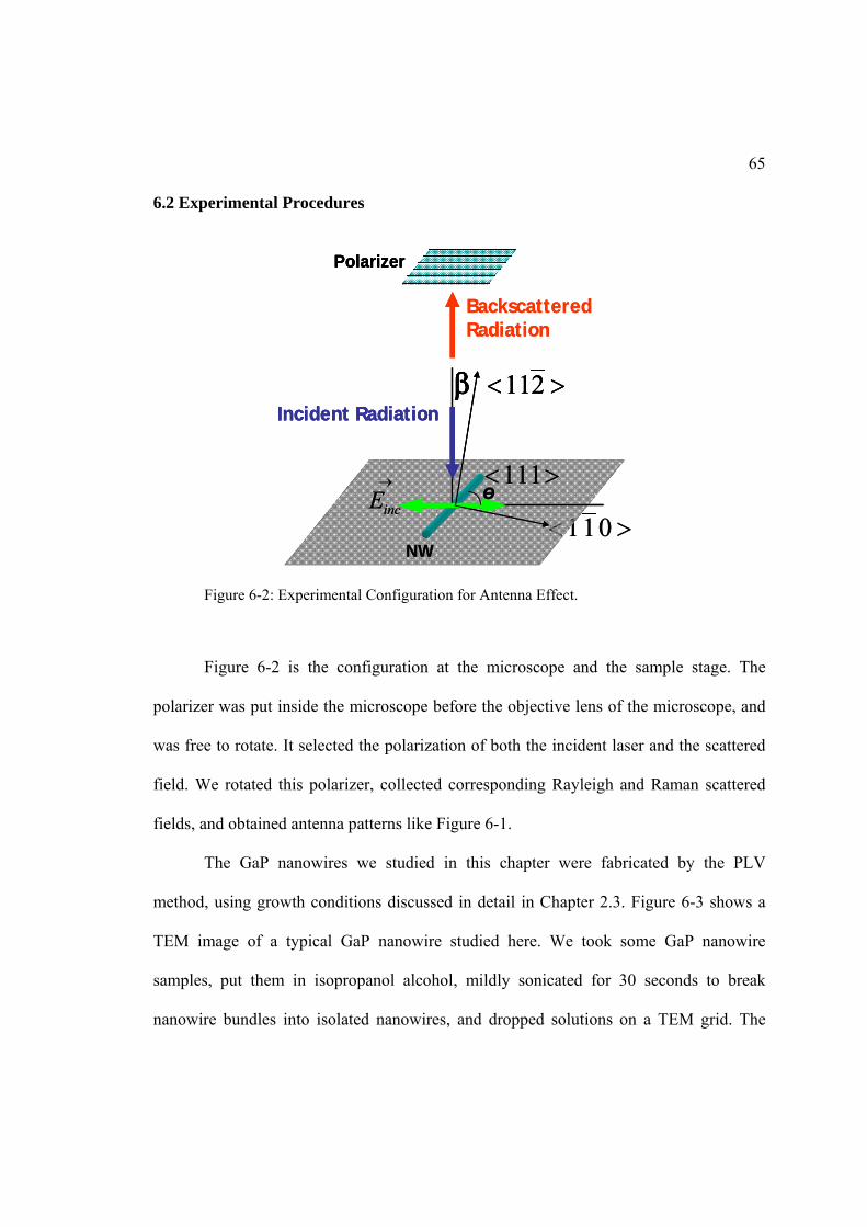
65
6.2 Experimental Procedures
Figure 6-2: Experimental Configuration for Antenna Effect.
Figure 6-2 is the configuration at the microscope and the sample stage. The
polarizer was put inside the microscope before the objective lens of the microscope, and
was free to rotate. It selected the polarization of both the incident laser and the scattered
field. We rotated this polarizer, collected corresponding Rayleigh and Raman scattered
fields, and obtained antenna patterns like Figure 6-1.
The GaP nanowires we studied in this chapter were fabricated by the PLV
method, using growth conditions discussed in detail in Chapter 2.3. Figure 6-3 shows a
TEM image of a typical GaP nanowire studied here. We took some GaP nanowire
samples, put them in isopropanol alcohol, mildly sonicated for 30 seconds to break
nanowire bundles into isolated nanowires, and dropped solutions on a TEM grid. The
>< 011
Backscattered Radiation
NW
өө
Polarizer
→
incE><111
>< 211Incident Radiation
β
>< 011
Backscattered Radiation
NW
өө
Polarizer
→
incE><111
>< 211Incident Radiation
β
NW
өө
Polarizer
→
incE><111
>< 211Incident Radiation
β
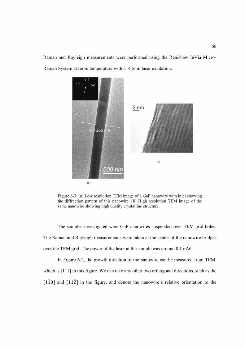
66
Raman and Rayleigh measurements were performed using the Renishaw InVia Micro-
Raman System at room temperature with 514.5nm laser excitation.
Figure 6-3: (a) Low resolution TEM image of a GaP nanowire with inlet showing the diffraction pattern of this nanowire. (b) High resolution TEM image of the same nanowire showing high quality crystalline structure.
The samples investigated were GaP nanowires suspended over TEM grid holes.
The Raman and Rayleigh measurements were taken at the center of the nanowire bridges
over the TEM grid. The power of the laser at the sample was around 0.1 mW.
In Figure 6-2, the growth direction of the nanowire can be measured from TEM,
which is [111] in this figure. We can take any other two orthogonal directions, such as the
[110] and [112] in the figure, and denote the nanowire’s relative orientation to the
67
incident laser by the angle which is between the incident laser and axis [112] in Figure
6-2.
6.3 Rayleigh and Raman Antenna Models
Here, I propose the models to explain the Rayleigh and Raman antenna patterns.
Since Rayleigh scattering can be treated as a special case of Raman scattering whose
Raman tensor is a unit tensor, we will focus on the Raman model.
6.3.1 Introduction to Rayleigh and Raman Antenna Models
As derived in Chapter 3.2, the dipole excited by an incident electromagnetic wave
is:
· . (6.1)
The intensity of radiation from this oscillating dipole is:
| · | | · · | | · · | , (6.2)
where is the incident light intensity inside sample, and is the Raman tensor, which is
defined as:
. (6.3)
For zincblende crystals, such as GaP, the Raman tensors for both LO and TO
mode are take the following form, but with different constants :
0 0 00 00 0
, (6.4)

68
0 00 0 0
0 0, (6.5)
0 00 0
0 0 0, (6.6)
where , and are the Raman tensor when the phonon displacement is
along , , and directions, respectively. , , and are along [100], [010] and [001]
crystallographic axes. [39].
For Rayleigh scattering, we simply use a unit matrix for the tensor .
In order to obtain the in eq. (6.2), we need to consider how light with different
polarization enters the nanowire.
Figure 6-4: Relation of electric field inside nanowire with the field outside nanowire.
In Figure 6-4, the horizontal red dashed lines label the nanowire axis. The electric
field at the vicinity outside the nanowire is polarized along a direction which makes an
angle with the nanowire axis. However, due to the geometry and aspect ratio of the
nanowire, usually the electric field inside the nanowire has a different polarization than
the field outside. We are able to write:
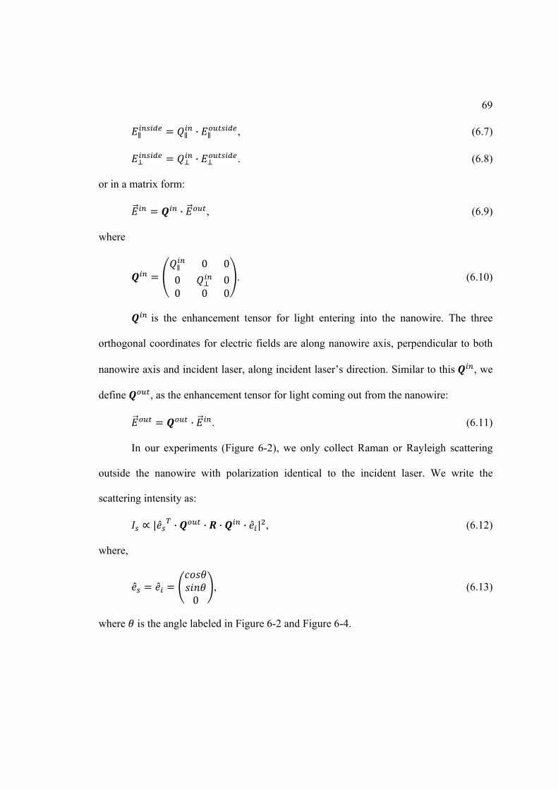
69
· , (6.7)
· . (6.8)
or in a matrix form:
· , (6.9)
where
0 00 00 0 0
. (6.10)
is the enhancement tensor for light entering into the nanowire. The three
orthogonal coordinates for electric fields are along nanowire axis, perpendicular to both
nanowire axis and incident laser, along incident laser’s direction. Similar to this , we
define , as the enhancement tensor for light coming out from the nanowire:
· . (6.11)
In our experiments (Figure 6-2), we only collect Raman or Rayleigh scattering
outside the nanowire with polarization identical to the incident laser. We write the
scattering intensity as:
| · · · · | , (6.12)
where,
0
, (6.13)
where is the angle labeled in Figure 6-2 and Figure 6-4.
70
In eq. (6.12), the Raman tensor can be determined if we know the nanowire’s
orientation relative to the incident laser. Therefore, the task left is to find the appropriate
enhancement tensor and .
6.3.2 Fitting Raman Antenna Patterns with Data from Experimental Rayleigh Antenna Patterns
It is pointed out by Linyou Cao and Bahram Nabet that since the difference in
frequency is small between Raman scattering and the incident laser, we can
approximately write [40]:
0 00 00 0 0
(6.14)
Therefore, the intensity for Rayleigh scattering, by eq. (6.10), is:
| · · · | (6.15)
Eq. (6.15) points out one way to obtain the enhancement tensor – from the
experimental Rayleigh antenna patterns. Once we have the enhancement tensor and the
growth direction of the nanowire, we only have one unknown parameter in the Raman
antenna model, the angle . We are able to find out this angle by trial and error, i.e.,
comparing calculated Raman antenna pattern with the experimental pattern. I will
elaborate the calculation below.
Referring to Figure 6-2 and Figure 6-4, we are going to introduce two sets of
coordinates. The first set, which we call lab coordinates , has its along nanowire axis,
along laser incident direction, and is perpendicular to both and . The second set is
71
the crystal coordinates ’, whose ’ is along crystallographic axis [100], ’ is along [010]
and ’ is along [001]. We denote, in ’, the growth direction as [ , , ], the axis
used to define angle with laser incident direction as [ , , ], and the axis
perpendicular to the previous two as [ , , ]. All these axis notations are
normalized. In Figure 6-2, [ , , ] is 1,1,1 /√3, [ , , ] is 1, 1,0 /√2,
and [ , , ] is 1,1, 2 /√6.
In coordinates ’, the laser is along:
. (6.16)
The in coordinates , written in coordinates , is:
. (6.17)
Now, we introduce the transform matrix , for any vertical vector , we have:
· . (6.18)
By picking , and as our , it is easy to obtain:
. (6.19)
Eq. (6.12) can be written in coordinates as:
|0
·0 0
0 00 0 0
· ·0 0
0 00 0 0
·0
| . (6.20)
Or, if we want to express the Raman tensor in coordinates :

72
|0
·0 0
0 00 0 0
· · · ·0 0
0 00 0 0
·0
| .
(6.21)
For Raman LO mode, referring to Eq. (6.4) – (6.6), we have the Raman tensor as:
0 0 00 0 10 1 0
0 0 10 0 01 0 0
0 1 01 0 00 0 0
.
(6.22)
Since in Eq. (6.4) – (6.6) is a constant and we are not comparing LO mode
intensity with TO mode intensity, we can treat it as “1” to check antenna patterns of LO
and TO modes separately, as what we do in Eq. (6.22).
For Raman TO modes, we have two orthogonal directions for TO phonon
displacement – along or direction.
0 0 00 0 10 1 0
0 0 10 0 01 0 0
0 1 01 0 00 0 0
. (6.23)
0 0 00 0 10 1 0
0 0 10 0 01 0 0
0 1 01 0 00 0 0
. (6.24)
Putting Eq. (6.21) – (6.24) together, we obtain the Raman LO and TO antenna
models as:
, |0
·0 0
0 00 0 0
· · · ·0 0
0 00 0 0
·0
| ,
(6.25)
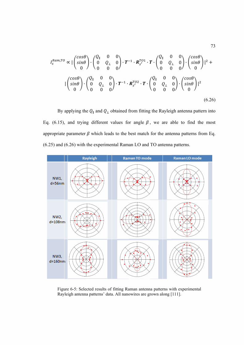
,
By
Eq. (6.15),
appropriate
(6.25) and (
FiguRay
|0
|0
·
applying th
, and tryin
e parameter
(6.26) with
ure 6-5: Seleyleigh antenn
·0
00 0
000 0
he and
ng different
which le
the experim
ected results na patterns’ d
0 00
0 0·
000
· ·
obtained f
t values fo
eads to the b
mental Ram
of fitting Radata. All nano
· ·
· ·
from fitting
or angle ,
best match
man LO and
aman antennowires are gr
·0
00 0
000 0
g the Rayleig
, we are a
for the ante
TO antenna
na patterns wrown along [
0 00
0 0·
000
·0
gh antenna
able to find
enna pattern
a patterns.
with experime[111].
73
0|
|
(6.26)
pattern into
d the most
ns from Eq
ental
3
)
o
t
.
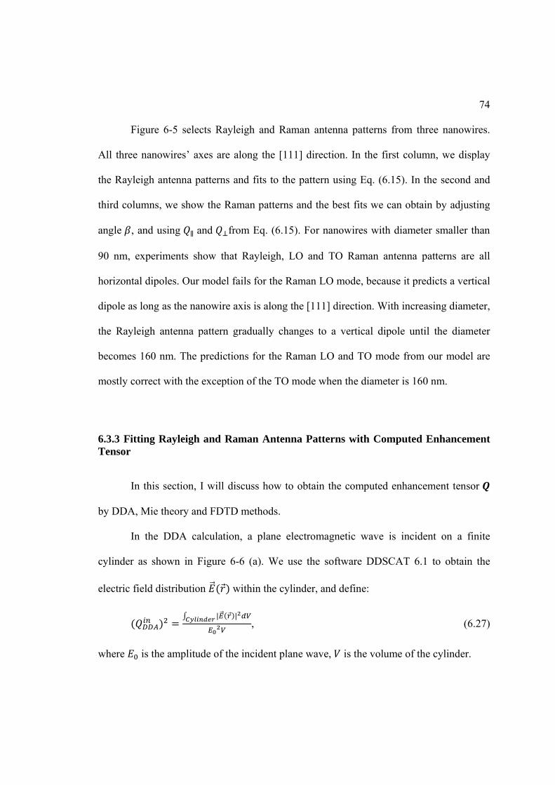
74
Figure 6-5 selects Rayleigh and Raman antenna patterns from three nanowires.
All three nanowires’ axes are along the [111] direction. In the first column, we display
the Rayleigh antenna patterns and fits to the pattern using Eq. (6.15). In the second and
third columns, we show the Raman patterns and the best fits we can obtain by adjusting
angle , and using and from Eq. (6.15). For nanowires with diameter smaller than
90 nm, experiments show that Rayleigh, LO and TO Raman antenna patterns are all
horizontal dipoles. Our model fails for the Raman LO mode, because it predicts a vertical
dipole as long as the nanowire axis is along the [111] direction. With increasing diameter,
the Rayleigh antenna pattern gradually changes to a vertical dipole until the diameter
becomes 160 nm. The predictions for the Raman LO and TO mode from our model are
mostly correct with the exception of the TO mode when the diameter is 160 nm.
6.3.3 Fitting Rayleigh and Raman Antenna Patterns with Computed Enhancement Tensor
In this section, I will discuss how to obtain the computed enhancement tensor
by DDA, Mie theory and FDTD methods.
In the DDA calculation, a plane electromagnetic wave is incident on a finite
cylinder as shown in Figure 6-6 (a). We use the software DDSCAT 6.1 to obtain the
electric field distribution within the cylinder, and define:
| |, (6.27)
where is the amplitude of the incident plane wave, is the volume of the cylinder.
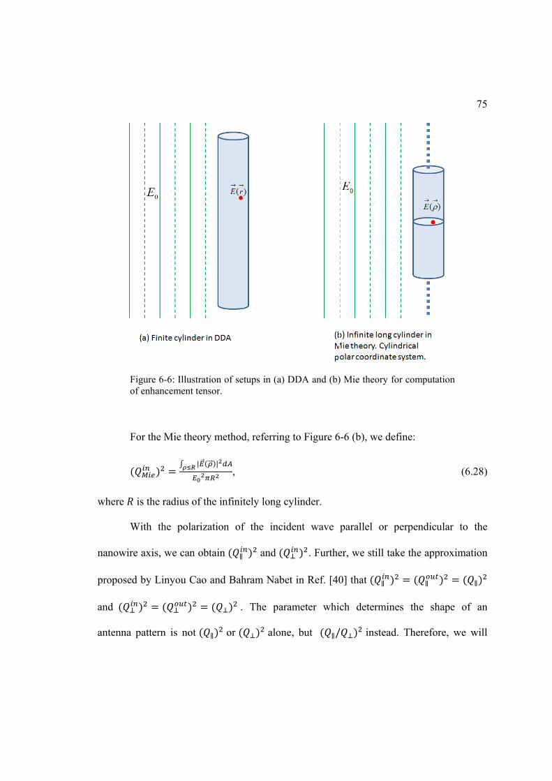
Figuof en
For
where is
Wit
nanowire a
proposed b
and
antenna pa
ure 6-6: Illusnhancement
the Mie the
the radius o
th the pola
axis, we can
y Linyou C
attern is not
stration of setensor.
eory method
| |,
of the infini
arization of
n obtain
Cao and Bah
.
t or
etups in (a) D
d, referring
tely long cy
f the incid
and
hram Nabet
The para
alone
DDA and (b)
to Figure 6
ylinder.
dent wave
. Furthe
t in Ref. [40
ameter whi
, but /
) Mie theory
6-6 (b), we d
parallel or
er, we still t
0] that
ch determi
/ instea
for computa
define:
perpendicu
take the app
ines the sh
ad. Therefo
75
ation
(6.28)
ular to the
proximation
hape of an
ore, we will
5
)
e
n
n
l
76
focus our discussions on , for DDA and Mie theory method. Eq. (6.15)
can be rewritten as:
(6.29)
In the Mie theory method, we only have one variable – the diameter and can
obtain the relation between / and the diameter . However, in the DDA method,
besides the variable , we also need to make a choice for the length of the cylinder.
Should it be the whole length of the nanowire, such as = 10 microns, or only part of
the nanowire illuminated by the incident light, such as = 1 micron? For the DDA work
carried out early in our group [41], research were conducted using 488 nm incident plane
wave and 2 microns long cylinder. Due to the uncertainty in choosing the correct length
for DDA computation discussed above, we haven’t done much DDA work since then and
have only limited results for 514 nm incident light. Therefore, for DDA calculation, I cite
our published results from the 2 micron long cylinder with 488nm incident excitation. In
Ref. [41], we compared the to the and plotted both in a graph similar as
Figure 6-7. The results from DDA and Mie theory share a lot of features, but we have a
strong unique peak from DDA when the diameter of the nanowire is around 85 nm. This
peak is most likely due to the resonance along nanowire axis when the polarization is
parallel to the axis, because from experimental Rayleigh data and Eq. (6.29), /
for = 92 nm is about 3.36. All fitted / from Eq. (6.29) will be shown later in
this chapter, together with , and .
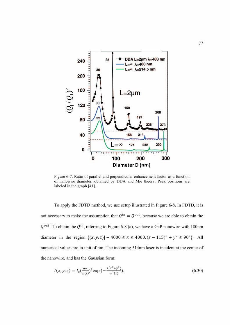
Figuof nlabe
To a
not necessa
. To ob
diameter in
numerical v
the nanowir
,
ure 6-7: Ratinanowire diaeled in the gr
apply the F
ary to make
btain the
n the regi
values are in
re, and has
, ,
io of parallelameter, obtaraph [41].
DTD metho
e the assump
, referring
on , ,
n unit of nm
the Gaussia
exp
l and perpenained by DD
od, we use s
ption that
g to Figure 6
| 4000
m. The inco
an form:
dicular enhaDA and Mie
setup illustr
,
6-8 (a), we
400
oming 514nm
.
ancement face theory. Pe
rated in Fig
because we
have a GaP
00, 115
m laser is in
ctor as a funcak positions
ure 6-8. In
e are able to
P nanowire w
5
ncident at th
77
ction s are
FDTD, it is
o obtain the
with 180nm
90 . All
he center of
(6.30)
7
s
e
m
l
f
)
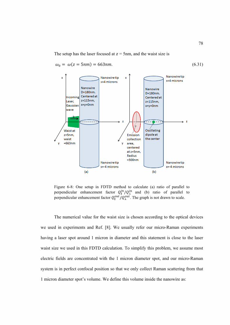
The
Figuperpperp
The
we used in
having a la
waist size w
electric fiel
system is in
1 micron di
e setup has t
ure 6-8: Onpendicular ependicular en
e numerical
n experimen
aser spot aro
we used in
lds are con
n perfect co
iameter spo
the laser foc
5 66
e setup in Fenhancementnhancement f
value for t
nts and Ref
ound 1 mic
this FDTD
ncentrated w
onfocal posi
ot’s volume.
cused at =
63 .
FDTD metht factor factor /
the waist siz
f. [8]. We u
cron in diam
calculation
with the 1 m
ition so that
We define
= 5nm, and t
hod to calcu/ and
/ . The g
ze is chosen
usually refe
meter and th
n. To simpli
micron diam
t we only c
this volum
the waist siz
ulate (a) rati(b) ratio
raph is not d
n according
fer our micr
his stateme
ify this prob
meter spot,
collect Ram
e inside the
ze is
io of paralleof parallel
drawn to scal
g to the opti
ro-Raman e
nt is close
blem, we as
and our mi
an scatterin
e nanowire a
78
(6.31)
el to l to le.
ical devices
experiments
to the laser
ssume most
icro-Raman
ng from that
as:
8
)
s
s
r
t
n
t
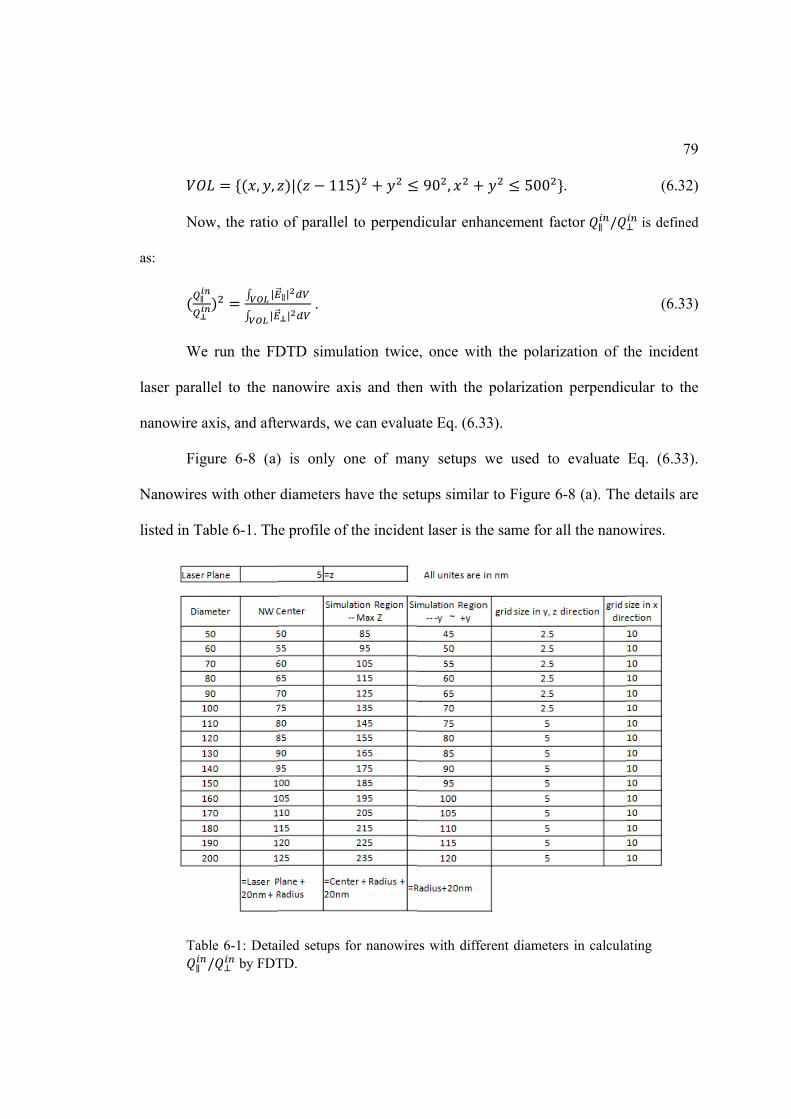
Now
as:
We
laser parall
nanowire ax
Figu
Nanowires
listed in Ta
Tab/
, ,
w, the ratio
|
|
run the FD
lel to the n
xis, and afte
ure 6-8 (a)
with other
able 6-1. Th
le 6-1: Deta/ by FDT
| 115
of parallel
|
| .
DTD simul
nanowire ax
erwards, we
) is only o
diameters h
e profile of
iled setups fTD.
5
l to perpend
ation twice
xis and then
e can evalua
one of man
have the set
f the inciden
for nanowire
90 ,
dicular enha
e, once with
n with the
ate Eq. (6.3
ny setups w
tups similar
nt laser is th
es with differ
500
ancement fa
h the polari
polarization
3).
we used to
r to Figure 6
he same for a
rent diamete
.
actor /
ization of t
n perpendic
o evaluate
6-8 (a). The
all the nano
ers in calcula
79
(6.32)
is defined
(6.33)
the incident
cular to the
Eq. (6.33)
e details are
owires.
ating
9
)
d
)
t
e
.
e
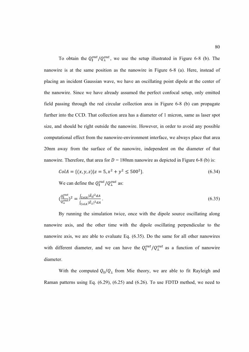
80
To obtain the / , we use the setup illustrated in Figure 6-8 (b). The
nanowire is at the same position as the nanowire in Figure 6-8 (a). Here, instead of
placing an incident Gaussian wave, we have an oscillating point dipole at the center of
the nanowire. Since we have already assumed the perfect confocal setup, only emitted
field passing through the red circular collection area in Figure 6-8 (b) can propagate
further into the CCD. That collection area has a diameter of 1 micron, same as laser spot
size, and should be right outside the nanowire. However, in order to avoid any possible
computational effect from the nanowire-environment interface, we always place that area
20nm away from the surface of the nanowire, independent on the diameter of that
nanowire. Therefore, that area for = 180nm nanowire as depicted in Figure 6-8 (b) is:
, , | 5, 500 . (6.34)
We can define the / as:
| |
| | . (6.35)
By running the simulation twice, once with the dipole source oscillating along
nanowire axis, and the other time with the dipole oscillating perpendicular to the
nanowire axis, we are able to evaluate Eq. (6.35). Do the same for all other nanowires
with different diameter, and we can have the / as a function of nanowire
diameter.
With the computed / from Mie theory, we are able to fit Rayleigh and
Raman patterns using Eq. (6.29), (6.25) and (6.26). To use FDTD method, we need to
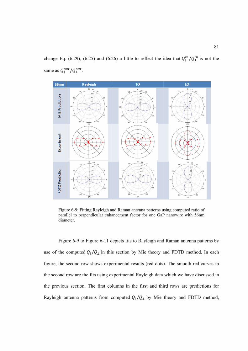
81
change Eq. (6.29), (6.25) and (6.26) a little to reflect the idea that / is not the
same as / .
Figure 6-9: Fitting Rayleigh and Raman antenna patterns using computed ratio of parallel to perpendicular enhancement factor for one GaP nanowire with 56nm diameter.
Figure 6-9 to Figure 6-11 depicts fits to Rayleigh and Raman antenna patterns by
use of the computed / in this section by Mie theory and FDTD method. In each
figure, the second row shows experimental results (red dots). The smooth red curves in
the second row are the fits using experimental Rayleigh data which we have discussed in
the previous section. The first columns in the first and third rows are predictions for
Rayleigh antenna patterns from computed / by Mie theory and FDTD method,
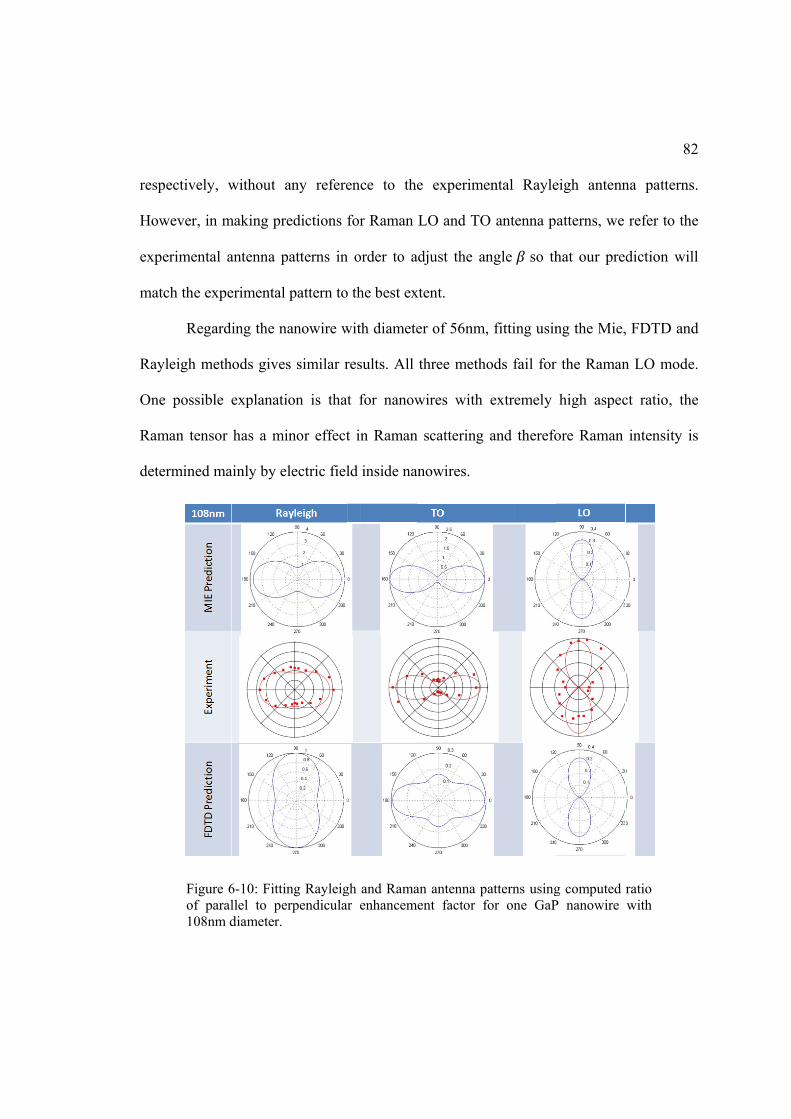
respectively
However, i
experiment
match the e
Reg
Rayleigh m
One possib
Raman ten
determined
Figuof p108n
y, without
in making p
tal antenna
experimenta
garding the
methods giv
ble explana
sor has a m
d mainly by
ure 6-10: Fitparallel to pnm diameter
any refere
predictions f
patterns in
al pattern to
nanowire w
ves similar r
ation is that
minor effect
electric fiel
tting Rayleigperpendicularr.
ence to the
for Raman
n order to a
o the best ex
with diamete
results. All
t for nanow
t in Raman
ld inside na
gh and Ramar enhancem
e experime
LO and TO
adjust the an
xtent.
er of 56nm,
three metho
wires with
n scattering
anowires.
an antenna pent factor f
ental Rayle
O antenna p
ngle so th
, fitting usin
ods fail for
extremely
and therefo
atterns usingfor one GaP
eigh antenn
atterns, we
hat our pred
ng the Mie,
r the Raman
high aspec
ore Raman
g computed rP nanowire
82
na patterns
refer to the
diction will
FDTD and
n LO mode
ct ratio, the
intensity is
ratio with
2 .
e
l
d
.
e
s
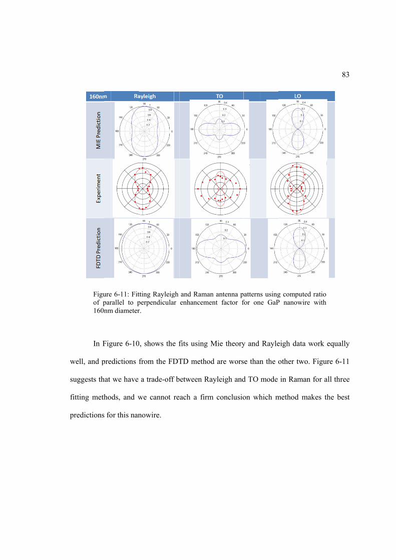
Figuof p160n
In F
well, and p
suggests th
fitting meth
predictions
ure 6-11: Fitparallel to pnm diameter
Figure 6-10
predictions f
hat we have
hods, and w
for this nan
tting Rayleigperpendicularr.
, shows the
from the FD
a trade-off
we cannot r
nowire.
gh and Ramar enhancem
e fits using
DTD metho
f between R
reach a firm
an antenna pent factor f
Mie theory
od are wors
Rayleigh and
m conclusio
atterns usingfor one GaP
y and Rayle
se than the o
d TO mode
on which m
g computed rP nanowire
eigh data w
other two. F
in Raman f
method mak
83
ratio with
work equally
Figure 6-11
for all three
kes the best
3
y
1
e
t

84
6.4 Discussion and Conclusion
By checking fits or predictions for three nanowires in the previous section, we
find that the FDTD method yields unsatisfactory results. Here, we further investigate the
difference among these three methods by focusing on , , ,
and from Eq. (6.28), (6.33), (6.35) and (6.29) respectively.
Figure 6-12: Log-linear scale of / vs. nanowire diameter, obtained in four different ways.
85
The four different / are plotted in a log-linear scale in Figure 6-12.
and yield the close answers for most of the nanowires measured
except the one with diameter of 160nm. This result implies that the large solid collection
angle arising from the use of 100x 0.95N.A. lens does not have a significant effect on our
polarized Raman experiments, since represents the result from considering
straight back scattering only while contains information from stray
scattering collected by the lens. The effect from large collection angle of the lens is
limited by the small back aperture of the lens together with restricting CCD collection
area to minimize the stray light.
In Figure 6-12, exhibits different behavior than the other three and we
find that the greatest discrepancy between and the others occurs when the
diameter of the nanowire is around 100nm. This is the case when the FDTD method fails
in Figure 6-10. This discrepancy, or this failure, comes from our over-simplified model to
compute .
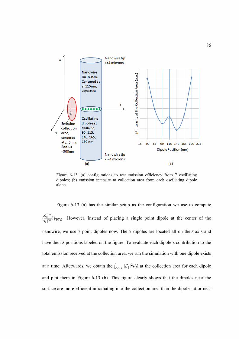
Figudipoalon
Figu
nanowire, w
have their
total emissi
at a time. A
and plot th
surface are
ure 6-13: (aoles; (b) emne.
ure 6-13 (a
. However
we use 7 p
positions
ion received
Afterwards,
hem in Figu
more effic
) configuratmission intens
a) has the
r, instead o
point dipole
labeled on
d at the coll
, we obtain
ure 6-13 (b
ient in radi
tions to test sity at colle
similar setu
of placing
es now. The
the figure. T
lection area,
the |
b). This fig
ating into th
emission eection area f
up as the c
a single po
e 7 dipoles
To evaluate
, we run the
| at th
gure clearly
he collectio
fficiency frofrom each o
configuratio
oint dipole
are located
e each dipol
e simulation
he collectio
y shows tha
on area than
om 7 oscillaoscillating di
on we use
e at the ce
d all on the
le’s contrib
n with one d
on area for
at the dipol
n the dipole
86
ating ipole
to compute
nter of the
e axis and
ution to the
dipole exists
each dipole
les near the
es at or near
6
e
e
d
e
s
e
e
r
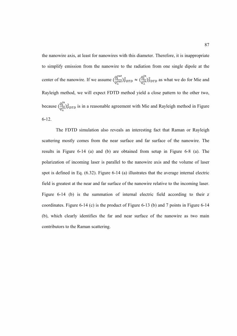
87
the nanowire axis, at least for nanowires with this diameter. Therefore, it is inappropriate
to simplify emission from the nanowire to the radiation from one single dipole at the
center of the nanowire. If we assume as what we do for Mie and
Rayleigh method, we will expect FDTD method yield a close pattern to the other two,
because is in a reasonable agreement with Mie and Rayleigh method in Figure
6-12.
The FDTD simulation also reveals an interesting fact that Raman or Rayleigh
scattering mostly comes from the near surface and far surface of the nanowire. The
results in Figure 6-14 (a) and (b) are obtained from setup in Figure 6-8 (a). The
polarization of incoming laser is parallel to the nanowire axis and the volume of laser
spot is defined in Eq. (6.32). Figure 6-14 (a) illustrates that the average internal electric
field is greatest at the near and far surface of the nanowire relative to the incoming laser.
Figure 6-14 (b) is the summation of internal electric field according to their
coordinates. Figure 6-14 (c) is the product of Figure 6-13 (b) and 7 points in Figure 6-14
(b), which clearly identifies the far and near surface of the nanowire as two main
contributors to the Raman scattering.
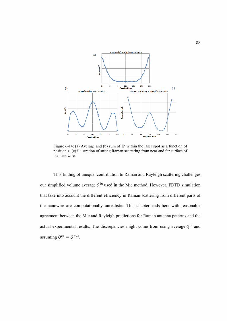
88
Figure 6-14: (a) Average and (b) sum of E2 within the laser spot as a function of position z; (c) illustration of strong Raman scattering from near and far surface of the nanowire.
This finding of unequal contribution to Raman and Rayleigh scattering challenges
our simplified volume average used in the Mie method. However, FDTD simulation
that take into account the different efficiency in Raman scattering from different parts of
the nanowire are computationally unrealistic. This chapter ends here with reasonable
agreement between the Mie and Rayleigh predictions for Raman antenna patterns and the
actual experimental results. The discrepancies might come from using average and
assuming .
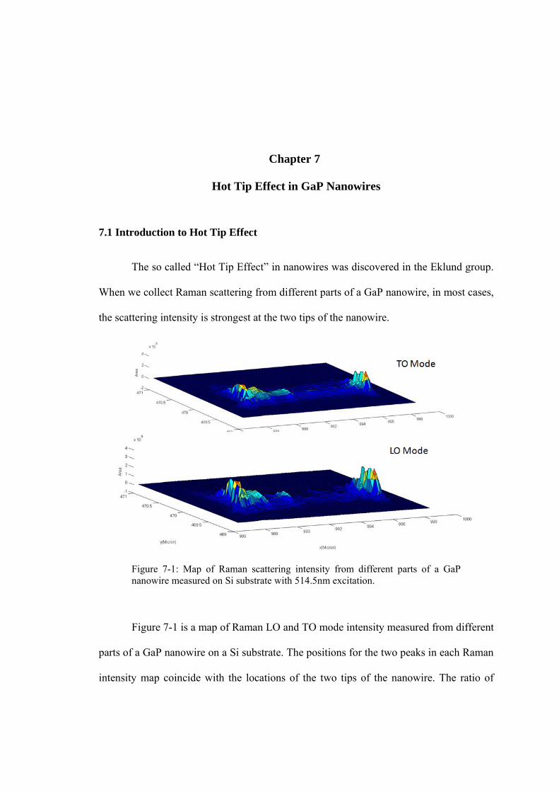
Chapter 7
Hot Tip Effect in GaP Nanowires
7.1 Introduction to Hot Tip Effect
The so called “Hot Tip Effect” in nanowires was discovered in the Eklund group.
When we collect Raman scattering from different parts of a GaP nanowire, in most cases,
the scattering intensity is strongest at the two tips of the nanowire.
Figure 7-1: Map of Raman scattering intensity from different parts of a GaP nanowire measured on Si substrate with 514.5nm excitation.
Figure 7-1 is a map of Raman LO and TO mode intensity measured from different
parts of a GaP nanowire on a Si substrate. The positions for the two peaks in each Raman
intensity map coincide with the locations of the two tips of the nanowire. The ratio of

90
Raman intensity at one tip to the intensity from the center is about 5 ~ 6 from the above
figure. Since we have s gold particle only at one tip of the nanowire, this hot tip effect
must be due to reasons other than the enhanced Raman scattering near a metal surface.
The detailed experimental procedures for such measurements will be discussed below.
7.2 Hot Tip Effect: Experimental Procedures for GaP Nanowires on Si Substrates
The GaP nanowires we studied in this section were fabricated by PLV, and the
growth conditions were discussed in detail in Chapter 2.3. We took some GaP nanowire
samples, put them in isopropanol alcohol, mildly sonicated for 30 seconds to break
nanowire bundles into isolated nanowires, and dropped the solutions onto a Si substrate.
The Raman measurements were performed using the Renishaw InVia micro-Raman
system.
Figure 7-2: 2D map scan setup for tip effect.
The Si substrate containing GaP nanowires is mounted on a computer-controlled
sample stage in the Renishaw InVia micro-Raman system. Figure 7-2 illustrates how the
sample stage moves to map the Raman scattering intensity. The laser spot is fixed and the
sample stag
scans, each
indicated by
Raman me
length.
Figusplitunde
The
to study. A
shown in F
one splittin
each mode
same nano
ge is free to
h separated b
y grey arrow
asurements
ure 7-3: (a)tting LO ander TO mode
e overall ma
At each grid
Figure 7-3 (
ng LO mode
varies a lo
owire. Ther
o move in x
by 50 nm ap
ws in Figur
in one x-s
) Typical Rd TO mode, aand the area
apping setup
point of tha
(a). The Ram
e and one su
ot among th
refore it is
and y direc
part. In each
re 7-2, and t
scan is 100
Raman spectand a SO moa under LO+S
p is like a 2
at 2D mesh
man spectru
urface optic
he Raman s
difficult to
ctions. A ty
h x-scan, th
the step betw
nm or 150
trum from aode; (b) SimpSO mode.
2D mesh cov
, we take a
um has thre
cal (SO) mo
spectra take
o use auto
ypical 2D m
e stage mov
ween two p
0 nm depen
a GaP nanoplified way t
vering the G
Raman spe
ee modes, o
de [42]. Ho
en from dif
fitting, an
map scan inc
ves from rig
ositions wh
nding on th
owire, incluto obtain the
GaP nanowi
ectrum, such
one splitting
owever, the
fferent posit
nd it is imp
91
cludes 20 x-
ght to left as
here we take
he nanowire
uding area
ire we want
h as the one
g TO mode
intensity of
tions of the
practical to
1
-
s
e
e
t
e
,
f
e
o
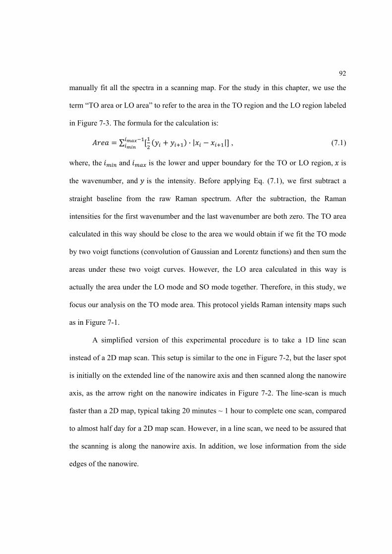
92
manually fit all the spectra in a scanning map. For the study in this chapter, we use the
term “TO area or LO area” to refer to the area in the TO region and the LO region labeled
in Figure 7-3. The formula for the calculation is:
∑ · | | , (7.1)
where, the and is the lower and upper boundary for the TO or LO region, is
the wavenumber, and is the intensity. Before applying Eq. (7.1), we first subtract a
straight baseline from the raw Raman spectrum. After the subtraction, the Raman
intensities for the first wavenumber and the last wavenumber are both zero. The TO area
calculated in this way should be close to the area we would obtain if we fit the TO mode
by two voigt functions (convolution of Gaussian and Lorentz functions) and then sum the
areas under these two voigt curves. However, the LO area calculated in this way is
actually the area under the LO mode and SO mode together. Therefore, in this study, we
focus our analysis on the TO mode area. This protocol yields Raman intensity maps such
as in Figure 7-1.
A simplified version of this experimental procedure is to take a 1D line scan
instead of a 2D map scan. This setup is similar to the one in Figure 7-2, but the laser spot
is initially on the extended line of the nanowire axis and then scanned along the nanowire
axis, as the arrow right on the nanowire indicates in Figure 7-2. The line-scan is much
faster than a 2D map, typical taking 20 minutes ~ 1 hour to complete one scan, compared
to almost half day for a 2D map scan. However, in a line scan, we need to be assured that
the scanning is along the nanowire axis. In addition, we lose information from the side
edges of the nanowire.
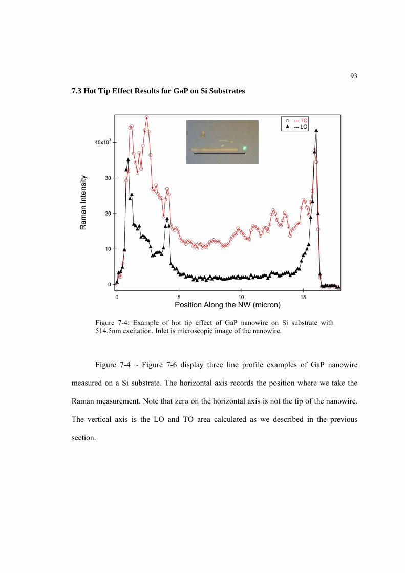
93
7.3 Hot Tip Effect Results for GaP on Si Substrates
Figure 7-4: Example of hot tip effect of GaP nanowire on Si substrate with 514.5nm excitation. Inlet is microscopic image of the nanowire.
Figure 7-4 ~ Figure 7-6 display three line profile examples of GaP nanowire
measured on a Si substrate. The horizontal axis records the position where we take the
Raman measurement. Note that zero on the horizontal axis is not the tip of the nanowire.
The vertical axis is the LO and TO area calculated as we described in the previous
section.
94
Figure 7-5: Example of hot tip effect of GaP nanowire on Si substrate with 514.5nm excitation. Inlets are microscopic images of the nanowire.
The insets in Figure 7-4 to Figure 7-6 are images taken by the microscope in the
Renishaw InVia micro-Raman system. The green dots in those images are laser spots.
The straight line in each image should be the scan path, but due to the imperfect
calibration of the coordinates for the laser spot, the path shown on these figures are off
the nanowire. In each experiment, the laser was always on the nanowire axis.

95
Figure 7-6: Example of non-hot tip effect of GaP nanowire on Si substrate with 514.5nm excitation. Inlets are microscopic images of the nanowire.
Figure 7-4 and Figure 7-5 shows the hot tip effect from a GaP nanowire on Si
substrate, while the nanowire in Figure 7-6 does not have hot tips. In fact, for all the
nanowires on Si substrate I have studied, about two-thirds of them exhibit hot tip effect.
Here, we define the enhancement factor (EF):
, , (7.2)
where is the intensity (TO area) around one tip, is the intensity around the other
tip, and is the intensity around the nanowire center. We use the function
here because a large enhancement may be caused by the gold particle at one tip. For most
96
GaP nanowires on Si substrate with hot tip effect, the enhancement factor is between 3
and 5.
Until now, we only know hot tip effect exists in most GaP nanowires on Si
substrate, and the enhancement factor varies among different nanowires. In the following
sections, we will study the GaP nanowires on TEM grid so that we have access to the tip
geometry of each nanowire from TEM images and we are able to remove any existing
effects from the interaction between the GaP nanowire and Si substrate. We will
experimentally study the correlation between the hot tip effect and the profile of the
incident laser, i.e., polarization and frequency of the incident laser. Further, we will
simulate the hot tip effect in the classical Raman scattering realm by the FDTD method
and obtain the expected enhancement factor. Afterwards, we can quantitatively judge
whether a nanowire has the hot tip effect or not, by using that expected enhancement
factor as a threshold to hot tip effect.
7.4 FDTD Simulation for Hot Tip Effect from GaP Nanowires
We assume that our GaP nanowire is single crystal and therefore the Raman
tensors at different parts of the nanowire are the same. To study the Raman intensity in
the classical realm, we only need to know how efficiently the laser enters into the
nanowire and how efficiently the oscillating dipole emission can emerge from the
nanowire and into the collection area.
The FDTD simulations in this chapter are very similar to the FDTD simulations in
the Chapter 6. With the incident laser polarization parallel/perpendicular to the nanowire
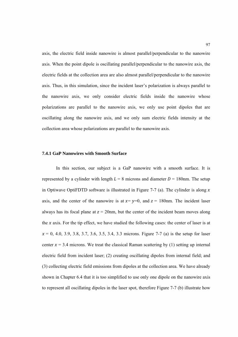
97
axis, the electric field inside nanowire is almost parallel/perpendicular to the nanowire
axis. When the point dipole is oscillating parallel/perpendicular to the nanowire axis, the
electric fields at the collection area are also almost parallel/perpendicular to the nanowire
axis. Thus, in this simulation, since the incident laser’s polarization is always parallel to
the nanowire axis, we only consider electric fields inside the nanowire whose
polarizations are parallel to the nanowire axis, we only use point dipoles that are
oscillating along the nanowire axis, and we only sum electric fields intensity at the
collection area whose polarizations are parallel to the nanowire axis.
7.4.1 GaP Nanowires with Smooth Surface
In this section, our subject is a GaP nanowire with a smooth surface. It is
represented by a cylinder with length = 8 microns and diameter = 180nm. The setup
in Optiwave OptiFDTD software is illustrated in Figure 7-7 (a). The cylinder is along
axis, and the center of the nanowire is at = =0, and = 180nm. The incident laser
always has its focal plane at = 20nm, but the center of the incident beam moves along
the axis. For the tip effect, we have studied the following cases: the center of laser is at
= 0, 4.0, 3.9, 3.8, 3.7, 3.6, 3.5, 3.4, 3.3 microns. Figure 7-7 (a) is the setup for laser
center = 3.4 microns. We treat the classical Raman scattering by (1) setting up internal
electric field from incident laser; (2) creating oscillating dipoles from internal field; and
(3) collecting electric field emissions from dipoles at the collection area. We have already
shown in Chapter 6.4 that it is too simplified to use only one dipole on the nanowire axis
to represent all oscillating dipoles in the laser spot, therefore Figure 7-7 (b) illustrate how
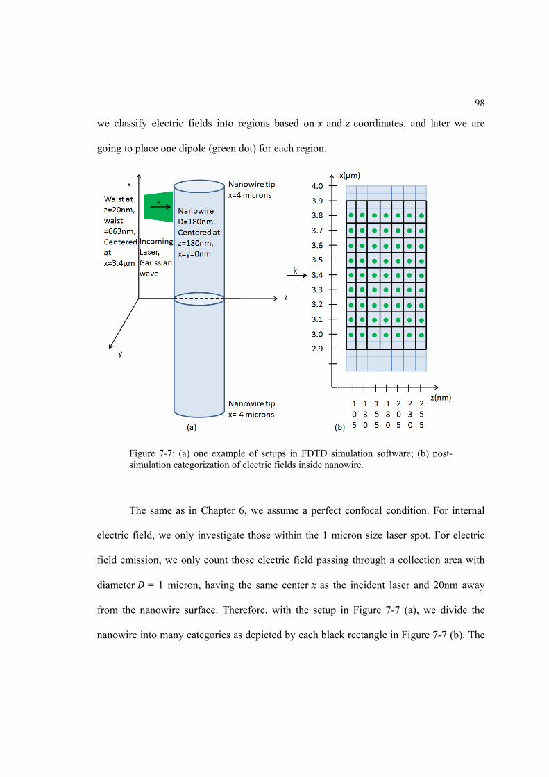
we classify
going to pla
Figusimu
The
electric fiel
field emiss
diameter
from the n
nanowire in
y electric fi
ace one dipo
ure 7-7: (a) ulation categ
e same as in
ld, we only
ion, we onl
= 1 micron
nanowire su
nto many ca
ields into r
ole (green d
one examplegorization of
n Chapter 6
y investigate
ly count tho
n, having t
urface. Ther
ategories as
regions base
dot) for each
e of setups electric field
6, we assum
e those with
ose electric
the same ce
refore, with
s depicted b
ed on and
h region.
in FDTD simds inside nan
me a perfec
hin the 1 m
field passi
enter as th
h the setup
by each blac
d coordin
mulation sofnowire.
t confocal
micron size
ng through
he incident
in Figure 7
ck rectangle
nates, and la
ftware; (b) p
condition. F
laser spot.
a collectio
laser and 2
7-7 (a), we
e in Figure 7
98
ater we are
post-
For internal
For electric
on area with
20nm away
e divide the
7-7 (b). The
8
e
l
c
h
y
e
e
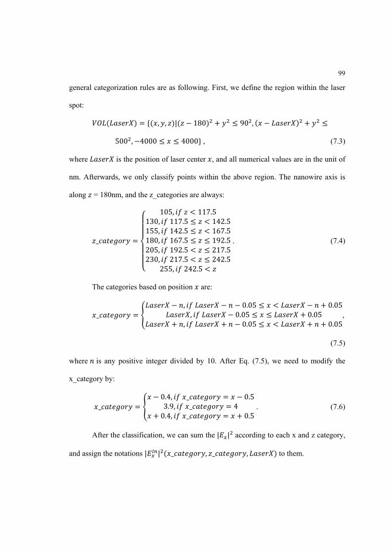
99
general categorization rules are as following. First, we define the region within the laser
spot:
, , | 180 90 ,
500 , 4000 4000 , (7.3)
where is the position of laser center , and all numerical values are in the unit of
nm. Afterwards, we only classify points within the above region. The nanowire axis is
along = 180nm, and the z_categories are always:
_
105, 117.5130, 117.5 142.5155, 142.5 167.5180, 167.5 192.5205, 192.5 217.5230, 217.5 242.5
255, 242.5
. (7.4)
The categories based on position are:
_, 0.05 0.05, 0.05 0.05
, 0.05 0.05,
(7.5)
where is any positive integer divided by 10. After Eq. (7.5), we need to modify the
x_category by:
_0.4, _ 0.53.9, _ 40.4, _ 0.5
. (7.6)
After the classification, we can sum the | | according to each x and z category,
and assign the notations | | _ , _ , to them.
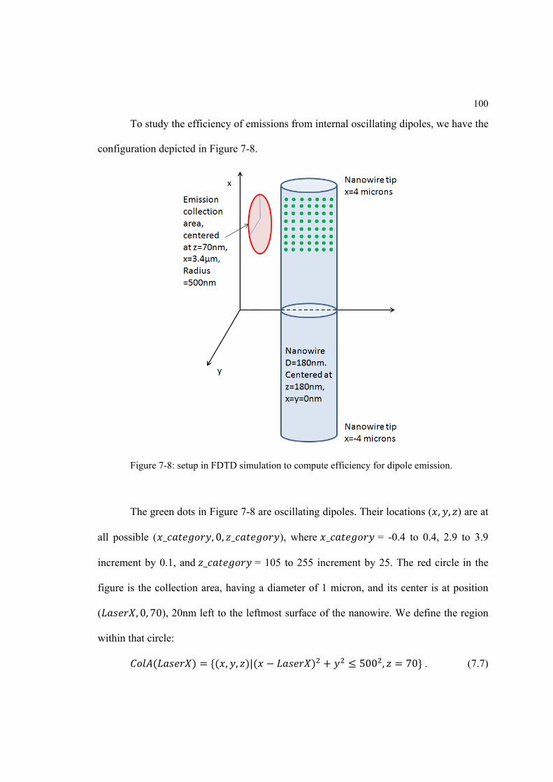
100
To study the efficiency of emissions from internal oscillating dipoles, we have the
configuration depicted in Figure 7-8.
Figure 7-8: setup in FDTD simulation to compute efficiency for dipole emission.
The green dots in Figure 7-8 are oscillating dipoles. Their locations ( , , ) are at
all possible ( _ , 0, _ ), where _ = -0.4 to 0.4, 2.9 to 3.9
increment by 0.1, and _ = 105 to 255 increment by 25. The red circle in the
figure is the collection area, having a diameter of 1 micron, and its center is at position
( , 0, 70), 20nm left to the leftmost surface of the nanowire. We define the region
within that circle:
, , | 500 , 70 . (7.7)
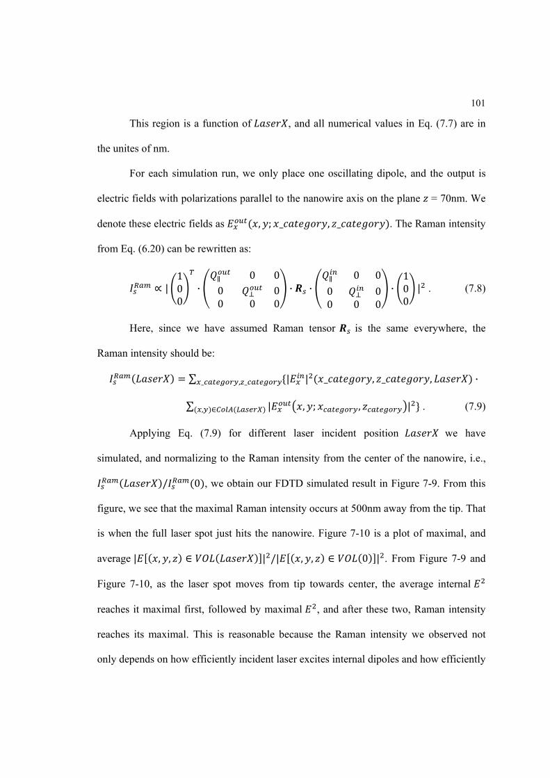
101
This region is a function of , and all numerical values in Eq. (7.7) are in
the unites of nm.
For each simulation run, we only place one oscillating dipole, and the output is
electric fields with polarizations parallel to the nanowire axis on the plane = 70nm. We
denote these electric fields as , ; _ , _ . The Raman intensity
from Eq. (6.20) can be rewritten as:
|100
·0 0
0 00 0 0
· ·0 0
0 00 0 0
·100
| . (7.8)
Here, since we have assumed Raman tensor is the same everywhere, the
Raman intensity should be:
∑ | | _ , _ , ·_ , _
∑ | , ; , |, . (7.9)
Applying Eq. (7.9) for different laser incident position we have
simulated, and normalizing to the Raman intensity from the center of the nanowire, i.e.,
/ 0 , we obtain our FDTD simulated result in Figure 7-9. From this
figure, we see that the maximal Raman intensity occurs at 500nm away from the tip. That
is when the full laser spot just hits the nanowire. Figure 7-10 is a plot of maximal, and
average | , , | /| , , 0 | . From Figure 7-9 and
Figure 7-10, as the laser spot moves from tip towards center, the average internal
reaches it maximal first, followed by maximal , and after these two, Raman intensity
reaches its maximal. This is reasonable because the Raman intensity we observed not
only depends on how efficiently incident laser excites internal dipoles and how efficiently
102
electric emission from internal oscillating dipoles can reach external detector, but also on
the volume of the nanowire illuminated by the laser.
Figure 7-9: Relative Raman intensity / 0 when laser incident on different positions of the GaP nanowire.
The enhancement factor obtained from these FDTD simulations is 1.40, much
smaller than the enhancement factor we observed in experimental results from GaP
nanowires on Si substrate. The possible explanations include: (1) in experiments, we have
additional enhancement from the interface of GaP nanowire and Si substrate; (2) in
experiments, the GaP nanowires have surface roughness along the nanowire; (3)
nanowire’s diameter may play an important role in enhancement factor, and this
calculated one (1.40) is only correct for nanowires whose diameters are 180nm; (4) real
nanowires have more complicated structures, such as twinnings and coatings.

103
Figure 7-10: Ratio of Max and Average internal E2 when laser is incident on the tip area to the corresponding value when laser is incident at the center of the nanowiere.
7.4.1 GaP Nanowires with Sinusoidal Surface Roughness
In the previous section, we assume our nanowires can be represented by a
cylinder. Here, we take into account the surface roughness along the nanowire. Instead of
a cylinder with length = 8 microns and diameter = 180nm, we model a nanowire with
400 small cylinders and each cylinder has a length of = 20 nm. Referring to the
coordinates in Figure 7-7 (a), the cylinder whose centers of tips locate at ( 4000
1 20,0,180 ) and ( 4000 20,0,180 ) has a diameter of
180 10 2 . All numerical values are in the unit of nm. Thus, in this model, the
nanowire has a sinusoidal surface roughness with wavelength of 400nm and amplitude of
10nm for diameter. The spatial computation step is 5nm in and direction, and 10 nm
in direction. Figure 7-11 shows the surface roughness near the tip by plotting the
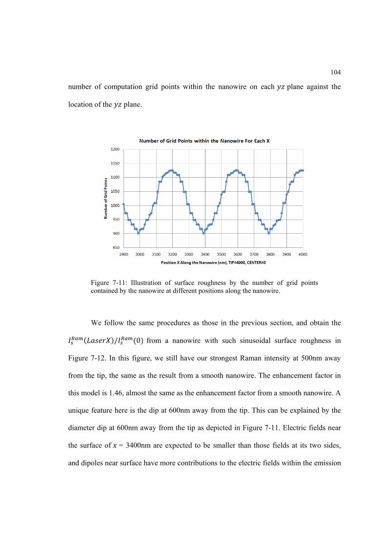
104
number of computation grid points within the nanowire on each plane against the
location of the plane.
Figure 7-11: Illustration of surface roughness by the number of grid points contained by the nanowire at different positions along the nanowire.
We follow the same procedures as those in the previous section, and obtain the
/ 0 from a nanowire with such sinusoidal surface roughness in
Figure 7-12. In this figure, we still have our strongest Raman intensity at 500nm away
from the tip, the same as the result from a smooth nanowire. The enhancement factor in
this model is 1.46, almost the same as the enhancement factor from a smooth nanowire. A
unique feature here is the dip at 600nm away from the tip. This can be explained by the
diameter dip at 600nm away from the tip as depicted in Figure 7-11. Electric fields near
the surface of = 3400nm are expected to be smaller than those fields at its two sides,
and dipoles near surface have more contributions to the electric fields within the emission
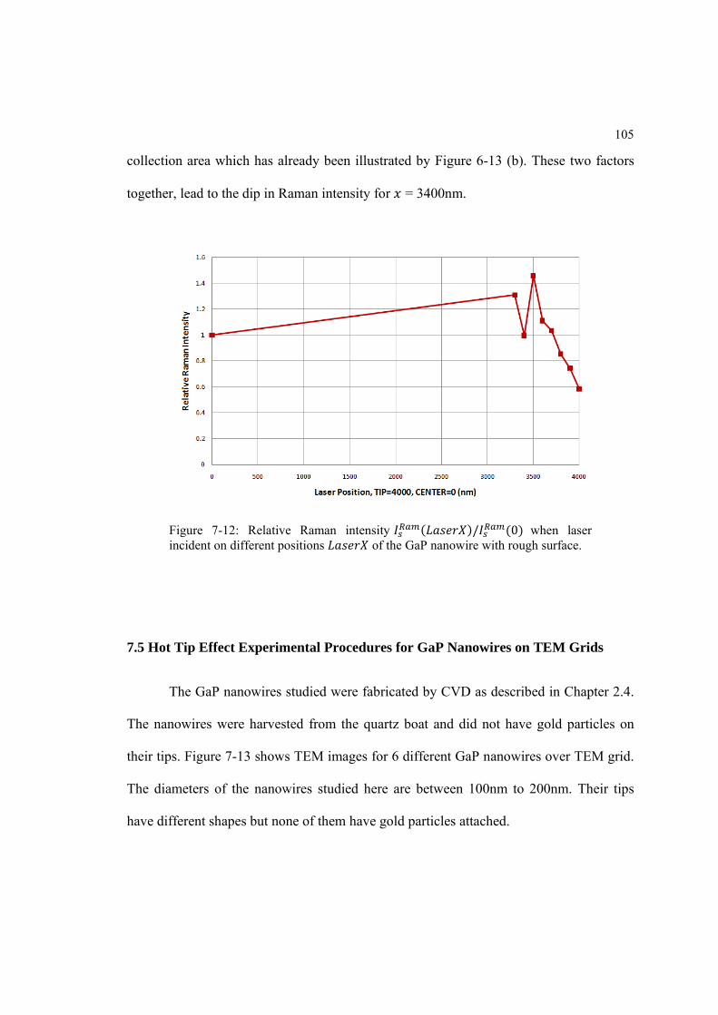
105
collection area which has already been illustrated by Figure 6-13 (b). These two factors
together, lead to the dip in Raman intensity for = 3400nm.
Figure 7-12: Relative Raman intensity / 0 when laser incident on different positions of the GaP nanowire with rough surface.
7.5 Hot Tip Effect Experimental Procedures for GaP Nanowires on TEM Grids
The GaP nanowires studied were fabricated by CVD as described in Chapter 2.4.
The nanowires were harvested from the quartz boat and did not have gold particles on
their tips. Figure 7-13 shows TEM images for 6 different GaP nanowires over TEM grid.
The diameters of the nanowires studied here are between 100nm to 200nm. Their tips
have different shapes but none of them have gold particles attached.
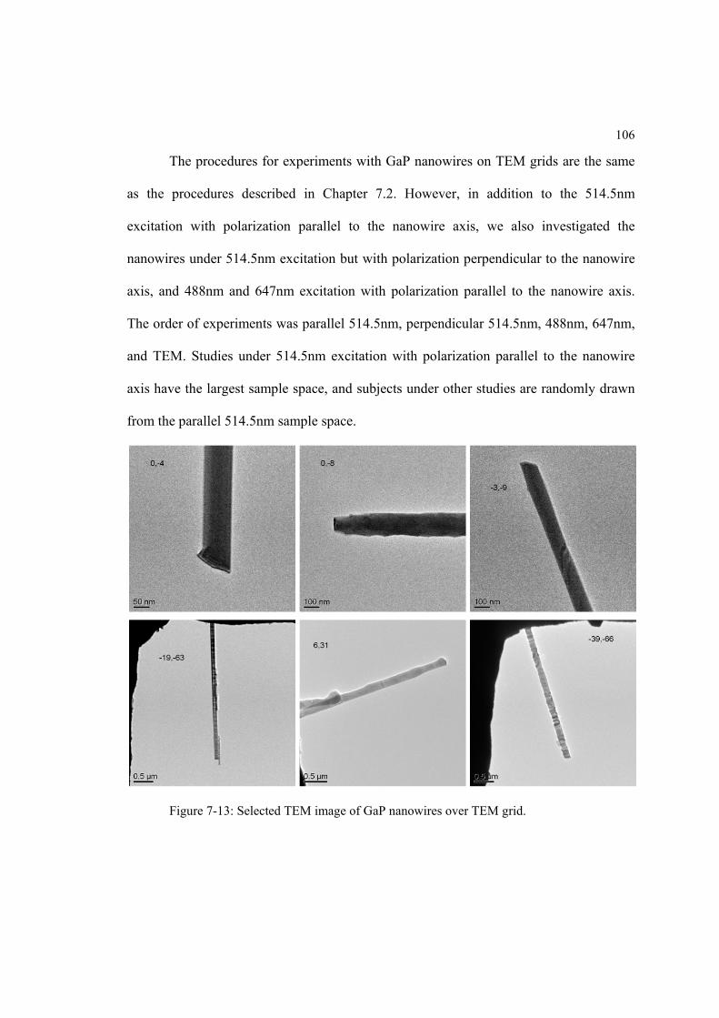
106
The procedures for experiments with GaP nanowires on TEM grids are the same
as the procedures described in Chapter 7.2. However, in addition to the 514.5nm
excitation with polarization parallel to the nanowire axis, we also investigated the
nanowires under 514.5nm excitation but with polarization perpendicular to the nanowire
axis, and 488nm and 647nm excitation with polarization parallel to the nanowire axis.
The order of experiments was parallel 514.5nm, perpendicular 514.5nm, 488nm, 647nm,
and TEM. Studies under 514.5nm excitation with polarization parallel to the nanowire
axis have the largest sample space, and subjects under other studies are randomly drawn
from the parallel 514.5nm sample space.
Figure 7-13: Selected TEM image of GaP nanowires over TEM grid.
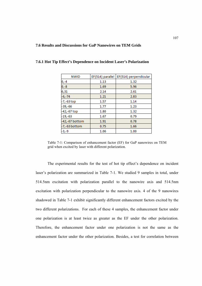
107
7.6 Results and Discussions for GaP Nanowires on TEM Grids
7.6.1 Hot Tip Effect’s Dependence on Incident Laser’s Polarization
Table 7-1: Comparison of enhancement factor (EF) for GaP nanowires on TEM grid when excited by laser with different polarization.
The experimental results for the test of hot tip effect’s dependence on incident
laser’s polarization are summarized in Table 7-1. We studied 9 samples in total, under
514.5nm excitation with polarization parallel to the nanowire axis and 514.5nm
excitation with polarization perpendicular to the nanowire axis. 4 of the 9 nanowires
shadowed in Table 7-1 exhibit significantly different enhancement factors excited by the
two different polarizations. For each of these 4 samples, the enhancement factor under
one polarization is at least twice as greater as the EF under the other polarization.
Therefore, the enhancement factor under one polarization is not the same as the
enhancement factor under the other polarization. Besides, a test for correlation between
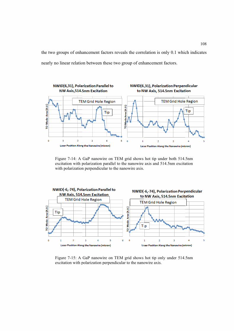
the two gro
nearly no li
Figuexciwith
Figuexci
oups of enha
inear relatio
ure 7-14: A itation with ph polarization
ure 7-15: A itation with p
ancement fa
on between
GaP nanowipolarization n perpendicu
GaP nanowipolarization p
actors revea
these two g
ire on TEM parallel to th
ular to the na
ire on TEM perpendicula
als the corre
group of enh
grid shows he nanowire anowire axis.
grid shows ar to the nano
elation is on
hancement f
hot tip undeaxis and 514
hot tip onlyowire axis.
nly 0.1 whic
factors.
er both 514.4.5nm excita
y under 514.
108
ch indicates
5nm ation
5nm
8
s
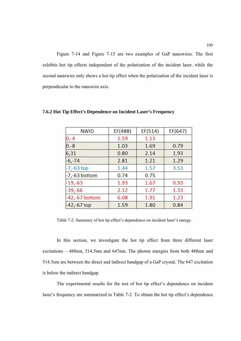
Figu
exhibits ho
second nan
perpendicu
7.6.2 Hot T
Tab
In t
excitations
514.5nm ar
is below the
The
laser’s freq
ure 7-14 an
ot tip effect
nowire only
lar to the na
Tip Effect’s
le 7-2: Summ
this section
– 488nm,
re between t
e indirect b
e experimen
quency are s
nd Figure
ts independ
shows a ho
anowire axi
s Dependen
mary of hot t
n, we inve
514.5nm an
the direct an
andgap.
ntal results
summarized
7-15 are tw
dent of the
ot tip effect
is.
nce on Incid
tip effect’s de
estigate the
nd 647nm.
nd indirect b
for the test
d in Table 7
wo exampl
polarization
when the p
dent Laser
ependence o
e hot tip e
The photon
bandgap of
t of hot tip
7-2. To obta
les of GaP
n of the inc
polarization
’s Frequen
n incident la
effect from
n energies
f a GaP crys
p effect’s de
ain the hot t
P nanowires
cident laser
of the incid
ncy
aser’s energy
m three diff
from both
stal. The 64
ependence
tip effect’s d
109
s. The first
r, while the
dent laser is
y.
ferent laser
488nm and
7 excitation
on incident
dependence
9
t
e
s
r
d
n
t
e
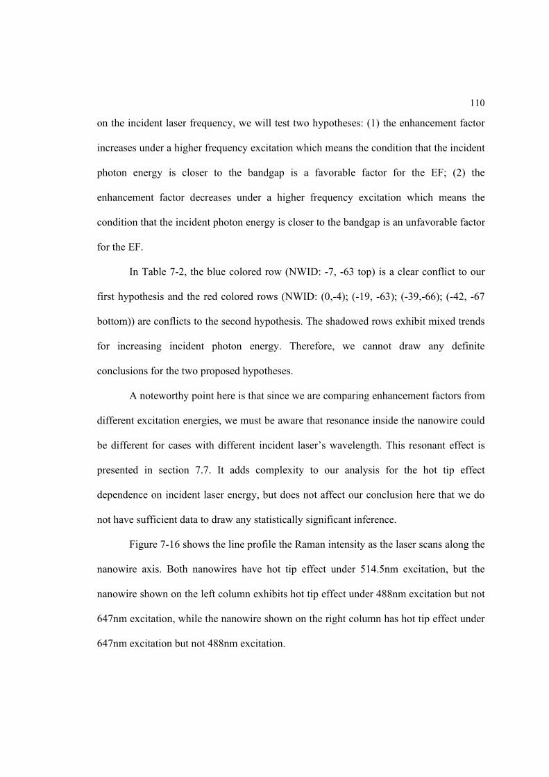
110
on the incident laser frequency, we will test two hypotheses: (1) the enhancement factor
increases under a higher frequency excitation which means the condition that the incident
photon energy is closer to the bandgap is a favorable factor for the EF; (2) the
enhancement factor decreases under a higher frequency excitation which means the
condition that the incident photon energy is closer to the bandgap is an unfavorable factor
for the EF.
In Table 7-2, the blue colored row (NWID: -7, -63 top) is a clear conflict to our
first hypothesis and the red colored rows (NWID: (0,-4); (-19, -63); (-39,-66); (-42, -67
bottom)) are conflicts to the second hypothesis. The shadowed rows exhibit mixed trends
for increasing incident photon energy. Therefore, we cannot draw any definite
conclusions for the two proposed hypotheses.
A noteworthy point here is that since we are comparing enhancement factors from
different excitation energies, we must be aware that resonance inside the nanowire could
be different for cases with different incident laser’s wavelength. This resonant effect is
presented in section 7.7. It adds complexity to our analysis for the hot tip effect
dependence on incident laser energy, but does not affect our conclusion here that we do
not have sufficient data to draw any statistically significant inference.
Figure 7-16 shows the line profile the Raman intensity as the laser scans along the
nanowire axis. Both nanowires have hot tip effect under 514.5nm excitation, but the
nanowire shown on the left column exhibits hot tip effect under 488nm excitation but not
647nm excitation, while the nanowire shown on the right column has hot tip effect under
647nm excitation but not 488nm excitation.
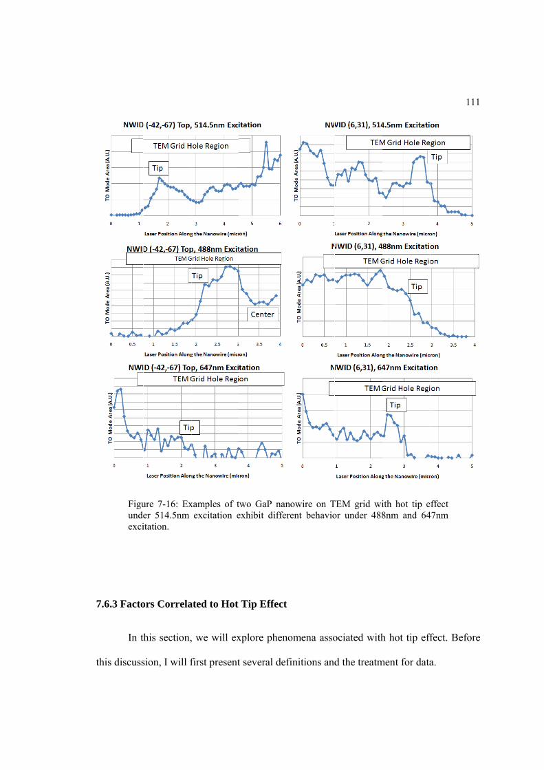
Figuundeexci
7.6.3 Facto
In th
this discuss
ure 7-16: Exer 514.5nm itation.
ors Correla
his section,
sion, I will f
xamples of texcitation e
ated to Hot
, we will ex
first present
two GaP nanexhibit differ
Tip Effect
xplore phen
t several def
nowire on Trent behavio
nomena asso
finitions and
TEM grid wior under 488
ociated with
d the treatm
ith hot tip e8nm and 64
h hot tip eff
ment for data
111
ffect 47nm
fect. Before
a.
1
e
112
Figure 7-17: Illustration of how to find tip and center on a Raman intensity line scan profile.
Since the tip position is not directly labeled on a Raman intensity line scan
profile, and the recorded scanned lines such as those in the insets of Figure 7-4 through
Figure 7-6 are usually not accurate due to imperfect stage coordinates calibration, we are
flexible in defining the “tip” in a Raman intensity line scan profile. We want to limit this
flexibility here so that we can have a uniform treatment for all data.
Figure 7-17 illustrates the procedures to mark the tip. From the FDTD simulations
in this chapter, we have learnt that starting from the tip until 500nm away from the tip,
the Raman intensity increases as the laser spot moves along the nanowire axis towards
the center. That result is based on the assumption that our laser spot is strictly 1 micron in
diameter. We release this restriction a little bit, and expect that the Raman intensity right
113
on the tip is a start point for a continuously increasing curve from a relative small value
to a regional maximal value within 800nm. Thus, the region between that starting point
and the regional maximal point is defined as “Tip Region”. We verify this region by two
ways. The recorded scanned lines such as those in the inlets of Figure 7-4 to Figure 7-6
are off the actual scanning lines, but they still provide useful information for possible
positions of the scanning start/end point and TEM grid edge. The position of TEM grid
edge can be further verified in a line scan profile as a sudden increasing of Raman
intensity around the possible point of TEM grid edge. The actual distance between TEM
grid edge and nanowire tip can be measured from TEM image. Therefore, we can check
the position of tip by tip’s distance to TEM grid edge and scanning start/end point.
From Figure 7-9, we have learnt that the Raman intensity decreases quickly after
the laser passes the maximal Raman intensity position for a smooth nanowire. Therefore,
on a Raman intensity line scan profile, we label the region containing the minimal
intensity as long as that position is at least 500nm away from the maximal intensity point
in the tip region to be the center region. We use the same number of points in the center
region as the number of points in the tip region.
As long as we are able to identify at least 5 points for the tip and center region,
respectively, we include that nanowire for our study. The nanowire may be
polycrystalline, may have a sharp tip or even a smaller nanowire attached to the tip
(NWID: -19,-63 in Figure 7-13).
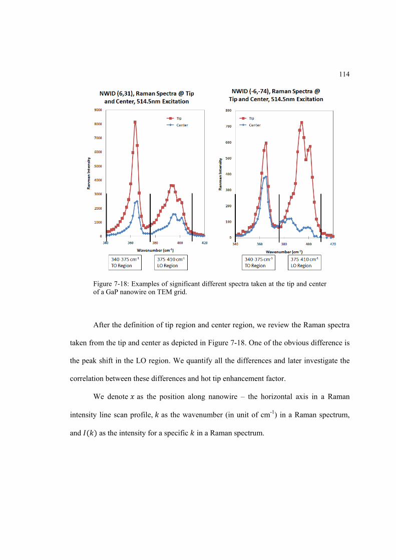
114
Figure 7-18: Examples of significant different spectra taken at the tip and center of a GaP nanowire on TEM grid.
After the definition of tip region and center region, we review the Raman spectra
taken from the tip and center as depicted in Figure 7-18. One of the obvious difference is
the peak shift in the LO region. We quantify all the differences and later investigate the
correlation between these differences and hot tip enhancement factor.
We denote as the position along nanowire – the horizontal axis in a Raman
intensity line scan profile, as the wavenumber (in unit of cm-1) in a Raman spectrum,
and as the intensity for a specific in a Raman spectrum.
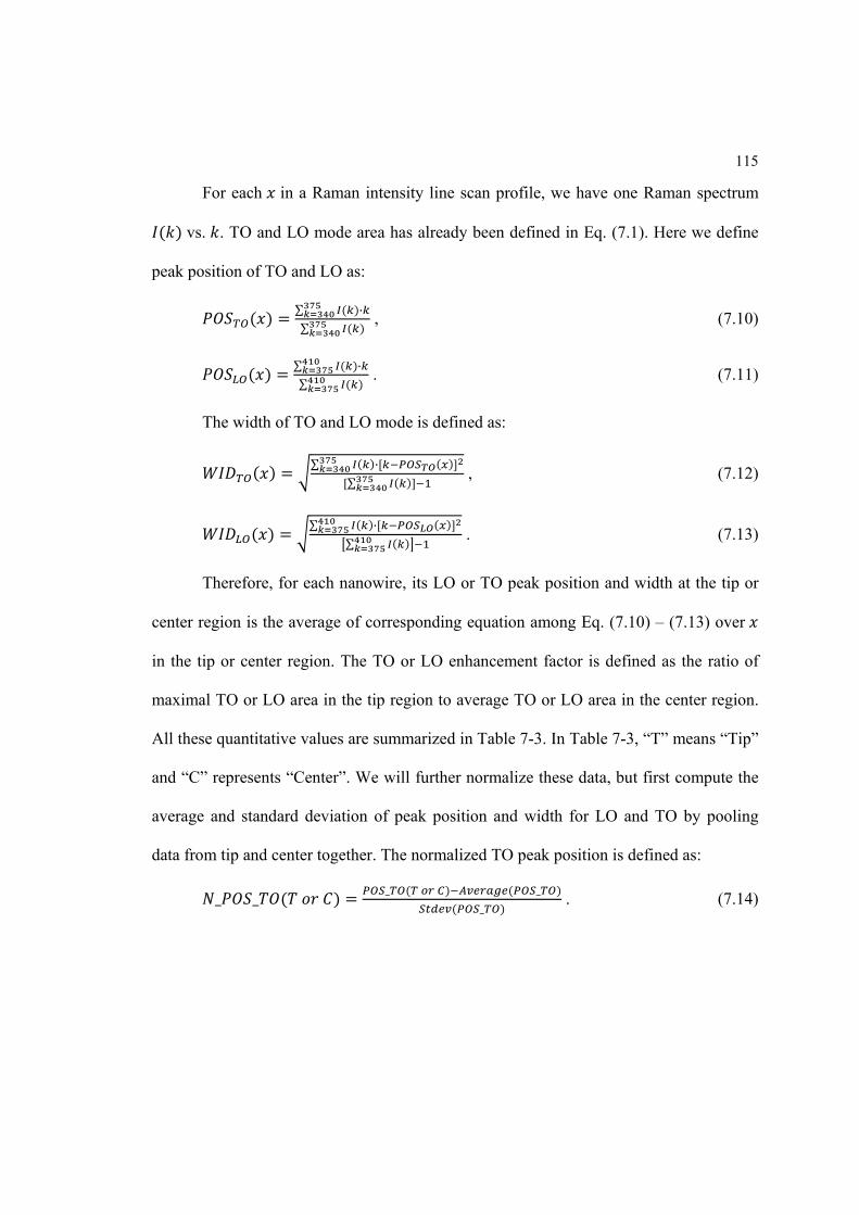
115
For each in a Raman intensity line scan profile, we have one Raman spectrum
vs. . TO and LO mode area has already been defined in Eq. (7.1). Here we define
peak position of TO and LO as:
∑ ·∑ , (7.10)
∑ ·∑ . (7.11)
The width of TO and LO mode is defined as:
∑ ·∑
, (7.12)
∑ ·∑ . (7.13)
Therefore, for each nanowire, its LO or TO peak position and width at the tip or
center region is the average of corresponding equation among Eq. (7.10) – (7.13) over
in the tip or center region. The TO or LO enhancement factor is defined as the ratio of
maximal TO or LO area in the tip region to average TO or LO area in the center region.
All these quantitative values are summarized in Table 7-3. In Table 7-3, “T” means “Tip”
and “C” represents “Center”. We will further normalize these data, but first compute the
average and standard deviation of peak position and width for LO and TO by pooling
data from tip and center together. The normalized TO peak position is defined as:
_ _ _ __
. (7.14)
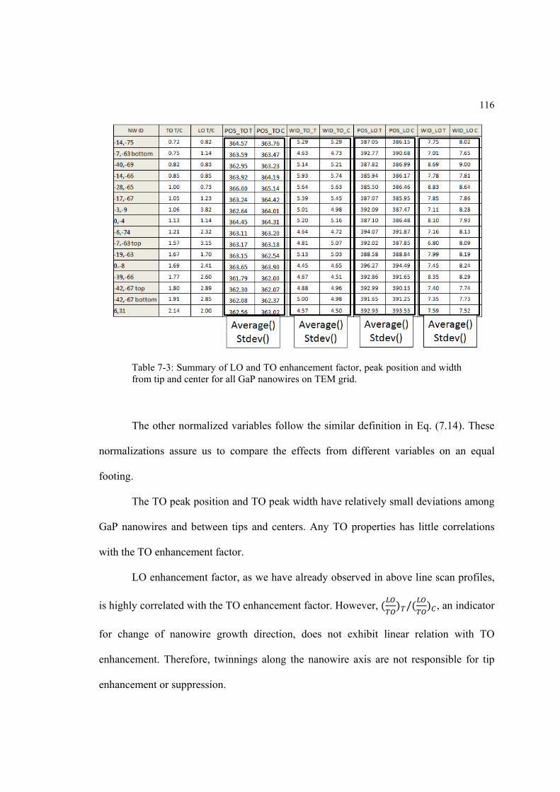
116
Table 7-3: Summary of LO and TO enhancement factor, peak position and width from tip and center for all GaP nanowires on TEM grid.
The other normalized variables follow the similar definition in Eq. (7.14). These
normalizations assure us to compare the effects from different variables on an equal
footing.
The TO peak position and TO peak width have relatively small deviations among
GaP nanowires and between tips and centers. Any TO properties has little correlations
with the TO enhancement factor.
LO enhancement factor, as we have already observed in above line scan profiles,
is highly correlated with the TO enhancement factor. However, / , an indicator
for change of nanowire growth direction, does not exhibit linear relation with TO
enhancement. Therefore, twinnings along the nanowire axis are not responsible for tip
enhancement or suppression.
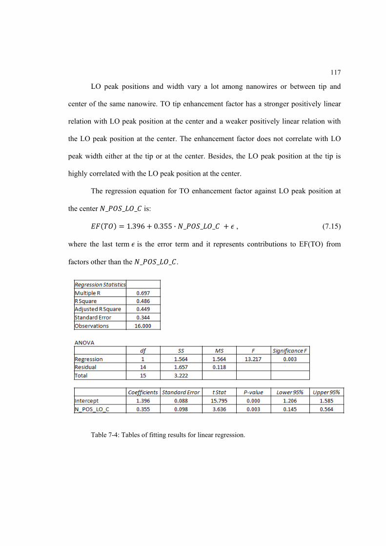
117
LO peak positions and width vary a lot among nanowires or between tip and
center of the same nanowire. TO tip enhancement factor has a stronger positively linear
relation with LO peak position at the center and a weaker positively linear relation with
the LO peak position at the center. The enhancement factor does not correlate with LO
peak width either at the tip or at the center. Besides, the LO peak position at the tip is
highly correlated with the LO peak position at the center.
The regression equation for TO enhancement factor against LO peak position at
the center _ _ _ is:
1.396 0.355 · _ _ _ , (7.15)
where the last term is the error term and it represents contributions to EF(TO) from
factors other than the _ _ _ .
Table 7-4: Tables of fitting results for linear regression.
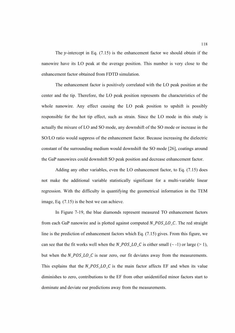
118
The -intercept in Eq. (7.15) is the enhancement factor we should obtain if the
nanowire have its LO peak at the average position. This number is very close to the
enhancement factor obtained from FDTD simulation.
The enhancement factor is positively correlated with the LO peak position at the
center and the tip. Therefore, the LO peak position represents the characteristics of the
whole nanowire. Any effect causing the LO peak position to upshift is possibly
responsible for the hot tip effect, such as strain. Since the LO mode in this study is
actually the mixure of LO and SO mode, any downshift of the SO mode or increase in the
SO/LO ratio would suppress of the enhancement factor. Because increasing the dielectric
constant of the surrounding medium would downshift the SO mode [26], coatings around
the GaP nanowires could downshift SO peak position and decrease enhancement factor.
Adding any other variables, even the LO enhancement factor, to Eq. (7.15) does
not make the additional variable statistically significant for a multi-variable linear
regression. With the difficulty in quantifying the geometrical information in the TEM
image, Eq. (7.15) is the best we can achieve.
In Figure 7-19, the blue diamonds represent measured TO enhancement factors
from each GaP nanowire and is plotted against computed _ _ _ . The red straight
line is the prediction of enhancement factors which Eq. (7.15) gives. From this figure, we
can see that the fit works well when the _ _ _ is either small (~ -1) or large (> 1),
but when the _ _ _ is near zero, our fit deviates away from the measurements.
This explains that the _ _ _ is the main factor affects EF and when its value
diminishes to zero, contributions to the EF from other unidentified minor factors start to
dominate and deviate our predictions away from the measurements.
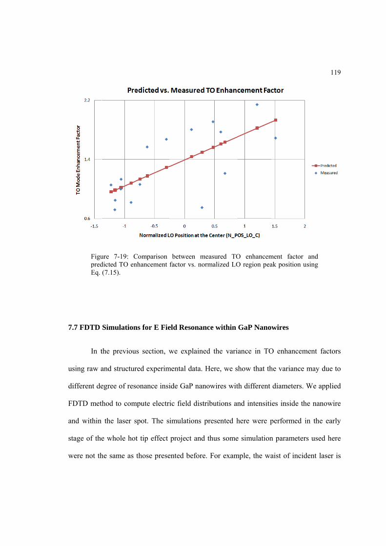
FigupredEq.
7.7 FDTD
In t
using raw a
different de
FDTD meth
and within
stage of the
were not th
ure 7-19: Cdicted TO en(7.15).
Simulation
the previou
and structur
egree of res
hod to com
the laser s
e whole hot
he same as
Comparison nhancement f
ns for E Fie
us section, w
red experim
sonance insi
mpute electri
spot. The si
t tip effect
those prese
between mfactor vs. no
eld Resonan
we explaine
mental data.
ide GaP nan
ic field dist
imulations
project and
ented before
measured TOormalized LO
nce within
ed the vari
Here, we s
nowires wit
tributions an
presented h
d thus some
e. For exam
O enhancemO region pea
GaP Nanow
ance in TO
show that th
th different
nd intensiti
here were p
e simulation
mple, the wa
ment factor ak position u
wires
O enhancem
he variance
diameters.
es inside th
performed i
n parameter
aist of incid
119
and using
ment factors
may due to
We applied
he nanowire
in the early
rs used here
dent laser is
9
s
o
d
e
y
e
s
220nm com
represent th
should not
other sectio
comparison
nanowires
certain diam
other nanow
Figu
In F
nanowire ti
nanowire a
mpared to th
he experime
be compar
ons. Beside
n of the to
with differe
meter we o
wires.
ure 7-20: E fi
Figure 7-20,
ip. Zero on
and 500 on t
he 663nm u
ental condi
red to eithe
s, the lengt
otal electric
ent diamete
observe rela
field resonanc
, the x-axis
the x-axis r
the x-axis m
used elsewh
tion and th
er the expe
th of the na
c field inten
ers, as illust
atively larg
ce inside GaP
records the
represents t
means that t
here in this
herefore the
rimental re
anowire used
nsity within
trated in Fi
ge resonanc
P nanowires
e position of
that the cent
the center o
dissertation
simulation
esults or the
d here is 10
n the laser
igure 7-20,
e compared
with differe
f incident la
ter of laser
f the laser s
n. This wai
n results in
e simulation
0 microns.
r spot insid
clearly sho
d to the res
ent diameters
aser spot rel
spot is at th
spot is on th
120
ist does not
this section
n results in
However, a
de the GaP
ows that for
sonances in
s.
lative to the
he tip of the
he nanowire
0
t
n
n
a
P
r
n
e
e
e
121
axis and 500nm away from the tip. The y-axis represents the sum of electric field
intensity within the laser spot and inside the nanowire when the center of the laser spot is
at x divided by the sum of electric field intensity when the center of the laser spot is at the
nanowire center (x=5000). For this set of simulations, a large resonance occurs when the
diameter of the nanowire is 150nm. Therefore, we believe that when certain conditions
meet, such as the relative position of laser to the nanowire tip and a combined
requirement for laser wavelength, nanoiwre’s diameter and length, there constructs a
strong electric resonance inside the nanowire and thus the nanowire exhibits a large
enhancement factor.
7.8 Conclusion
The hot tip effect for GaP nanowires grown by either PLV or CVD method is not
correlated with the polarization of the incident laser, nor does it correlate with the
incident laser’s energy. The theoretical enhancement factor is 1.40 for a well-shaped
smooth nanowire and this value is in good agreement with the y-intercept in the fit of
experimental data from GaP nanowires on TEM grids. Electric field resonance inside
nanowire is a possible explanation to the variance of enhancement factors among
nanowires. Other underlying factors increasing or decreasing the EF remain unknown.
However, we know from the fit that the underlying factor(s) should also affect the peak
positions of the LO or SO mode or the relative intensity of LO/SO. The mechanism for
additional enhancement from GaP on Si substrate hasn’t been studied yet. There is a long
journey ahead for a thorough understanding of the hot tip effect.
References
1. Lu, W., et al., Nanoelectronics from the bottom up. Nature Materials, 2007. 6: p. 841 – 850.
2. Wagner, R. S., et al., Vapor-Liqui-Solid Mechanism of Single Crystal Growth. Applied Physics Letters, 1964. 4(5): p. 89-90.
3. Wu, Y., et al., Direct Observation of Vapor-Liquid- Solid Nanowire Growth. Journal of Chemical Society, 2001. 123(13): p. 3165-3166.
4. Lew, K.K., et al., Vapor-Liquid-Solid Growth of Silicon-Germanium Nanowires. Anvanced Materials, 2003. 15(24): p. 2073-2076.
5. Adu, K. W., Synthesis and Raman Scattering Studies of Novel Semiconductor Nanostructures:Si , Ge and GaAs Twinning Superlattice Nanowires. Ph.D. Thesis, 2004.
6. Long, D. A., The Raman Effect: A Unified Treatment of the Theory of Raman Scattering by Molecules. 2002, West Sussex: John Wiley & Sons.
7. Horiba Jobin Yvon T64000 manual. Horiba Ltd. 8. Renishaw InVia Micro-Raman System Manual. Renishaw Plc. 9. Meyer, D. J., et al., Applications and processing of SiGe and SiGe:C for high-
speed HBT devices. Materials Science in Semiconductor Processing, 2001. 4(6): p. 529-533.
10. Paul, D. J., Silicon germanium heterostructures in electronics: the present and the future. Thin Solid Films, 1998. 321(1-2): p. 172-180.
11. Yang, J. E., et al., Band-Gap Modulation in Single-Crystalline Si1-xGex Nanowires. Nano Letters, 2006. 6(12): p.2679-2684.
12. Lee, J., et al., Responsivity and impact ionization coefficients of Si1-xGex photodiodes. IEEE Transactions on Electron Devices, 1996. 43(6): p. 977-981.
13. Weber, J., et al., Near-band-gap photoluminescence of Si-Ge alloys. Physical Review B, 1989. 40(8): p. 5683-5693.
14. Giannozzi, P., et al., Ab initio calculation of phonon dispersions in semiconductors. Physical Review B, 1991. 43(9): p. 7231-7242.
15. Beraud, A., et al., Disorder-induced broadening of transverse acoustic phonons in SixGe1−x mixed crystals. Physica B, 2004. 350(1-3): p. 254-257.
16. Rat, E., et al., Disorder broadening of the acoustic branches in SixGe1−x mixed crystals. Physica B, 2000. 276-278: p. 429-430.
17. Molinas-Mata, P., et al., Phonon dispersion relations for Ge/Si superlattices grown along the [100] and [111] directions. Superlattices and Microstructures, 1991. 10(1): p. 39-46.
123
18. Molinari, E., et al., Calculated phonon spectra of Si/Ge (001) superlattices:
Features for interface characterization. Applied Physics Letters, 1989. 54(13): p.1220-1222.
19. Ren, S. F., et al., Microscopic investigation of phonon modes in SiGe alloy nanocrystals. Physical Review B, 2004. 69(23): p. -.
20. Alonso, M. I., et al., Raman spectra of c-Si1-xGex alloys. Physical Review B, 1988. 39(14): p. 10056-10062.
21. Sharma, V., et al., Optical Properties of Ge Nanowires Grown on Silicon (111) and (100) Substrates. Materials Research Society Symposium Proceedings, 2005. 832: p. 329-334.
22. Kolobov, A. V., Raman scattering from Ge nanostructures grown on Si substrates: Power and limitations. Journal of Applied Physics, 2000. 87(6): p. 2926-2930.
23. Sheng, C., et al., Suppression of Si-Ge interfacial vibration mode in the Raman spectrum of a Si6Ge4 superlattice. Physical Review B, 1996. 53(16): p. 10771–10774.
24. Watanabe, M., et al., Absorption correction and thickness determination using the ζ factor in quantitative X-ray microanalysis. Ultramicroscopy, 1996. 65(3-4): p. 187-198.
25. Xiong, Q., et al., Raman Scattering from Surface Phonons in Rectangular Cross-sectional w-ZnS Nanowires. Nano Letters, 2004. 4(10): p. 1991-1996.
26. Gupta, R., et al., Surface Optical Phonons in Gallium Phosphide Nanowires. Nano Letters, 2003. 3(12): p 1745–1750.
27. Zhang, X., et al., Diameter-Dependent Composition of Vapor-Liquid-Solid Grown Si1-xGex Nanowires. Nano Letters, 2007. 7(10): p. 3241-3245.
28. Kim, J. M., et al., Two-Photon Photopolymerized Tips for Adhesion-Free Scanning-Probe Microscopy. Nano Letters, 2005. 5(2): p. 309–314.
29. Zhang, Z., et al., Raman scattering from surface optical phonon mode in gallium phosphide nanomaterials. Journal of Nanopartical Research, 2010. 12(3): p. 961-966.
30. Lew, K. K., et al., Effect of Growth Conditions on the Composition and Structure of Si1-xGex Nanowires Grown by vapor-Liquid-Solid Growth. Journal of Materials Research, 2006. 21(11): p. 2876-2881.
31. Nishimura, C., et al., Raman Characterization of Ge Distribution in Individual Si1-xGex Alloy Nanowires. Applied Physics Letters, 2008. 93(20): p. -.
32. Bohren, C. F., et al., Absorption and Scattering of Light by Small Particles. 1983, New York: John Wiley & Sons.
33. Draine, B. T., et al., Beyond Clausius-Mossotti: Wave Propagation on a Polarizable Point Lattice and the Discrete Dipole Approximation. The Astrophysical Journal, 1993. 405: p. 685-697.
34. Goodman, J. J., et al., Application of fast-Fourier-transform techniques to the discrete-dipole approximation. Optics Letters, 1991. 16(15): p. 1198-1200.
124
35. Draine, B. T., et al., User Guide for the Discrete Dipole Approximation Code
DDSCAT 6.1. http://arxiv.org/abs/astro-ph/0409262. 36. OptiFDTD Technique Background and Tutorials. Optiwave Systems Inc. 37. Ajiki, H, et al., Carbon Nanotubes – Optical Absorption in Aharonov-Bohm Flux.
Japanese Journal of Applied Physics, 1994. 34(1): p. 107-109. 38. Ajiki, H., et al., Aharonov-Bohm effect on magnetic properties of carbon
nanotubes. Physica B, 1996. 216B(3-4): p. 358-361. 39. Yu, P. Y., et al., Fundamentals of semiconductors : physics and materials
properties. 2001, Berlin ; New York: Springer. 40. Cao, L., et al., Enhanced Raman Scattering from Individual Semiconductor
Nanocones and Nanowires. Physical Review Letters, 2006. 96(15): p. -. 41. Chen, G., et al., Optical Antenna Effect in Semiconducting Nanowires. Nano
Letters, 2008. 8(5): p. 1341-1346. 42. Xiong, Q., et al., Raman scattering studies of individual polar semiconducting
nanowires: phonon splitting and antenna effects. Applied Physics A, 2006. 85(3): p. 299-305.
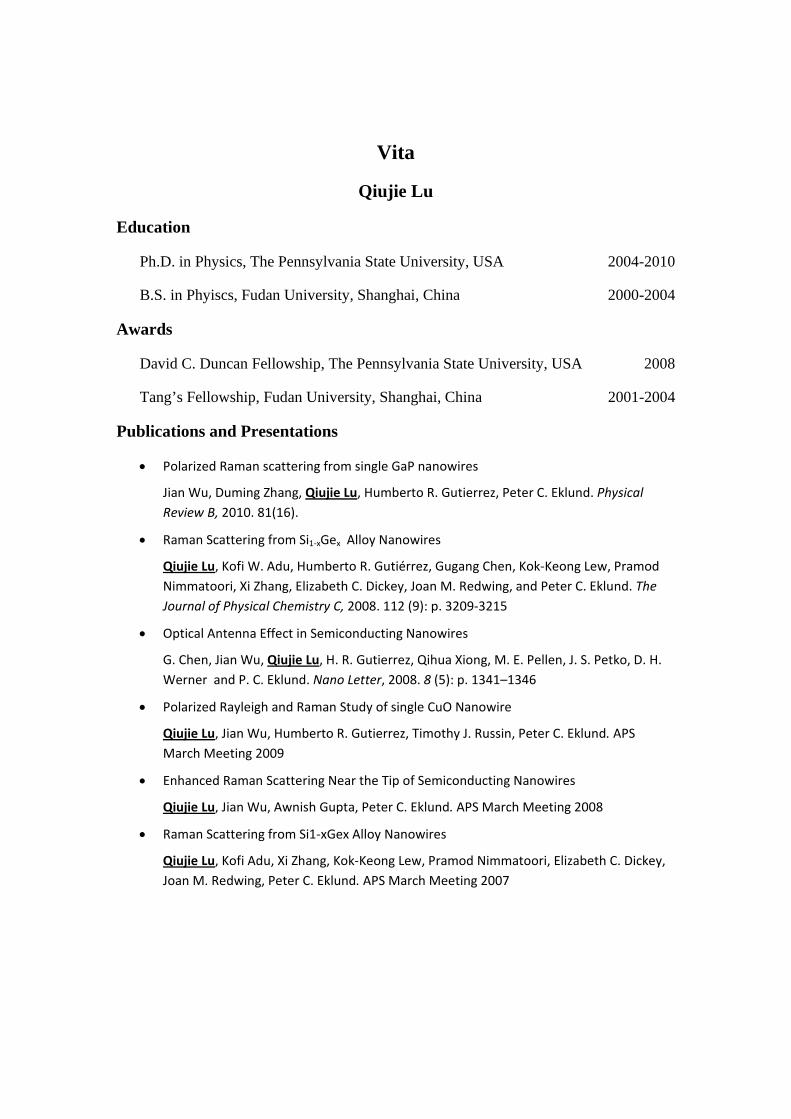
Vita
Qiujie Lu
Education
Ph.D. in Physics, The Pennsylvania State University, USA 2004-2010
B.S. in Phyiscs, Fudan University, Shanghai, China 2000-2004
Awards
David C. Duncan Fellowship, The Pennsylvania State University, USA 2008
Tang’s Fellowship, Fudan University, Shanghai, China 2001-2004
Publications and Presentations
• Polarized Raman scattering from single GaP nanowires
Jian Wu, Duming Zhang, Qiujie Lu, Humberto R. Gutierrez, Peter C. Eklund. Physical Review B, 2010. 81(16).
• Raman Scattering from Si1‐xGex Alloy Nanowires
Qiujie Lu, Kofi W. Adu, Humberto R. Gutiérrez, Gugang Chen, Kok‐Keong Lew, Pramod Nimmatoori, Xi Zhang, Elizabeth C. Dickey, Joan M. Redwing, and Peter C. Eklund. The Journal of Physical Chemistry C, 2008. 112 (9): p. 3209‐3215
• Optical Antenna Effect in Semiconducting Nanowires
G. Chen, Jian Wu, Qiujie Lu, H. R. Gutierrez, Qihua Xiong, M. E. Pellen, J. S. Petko, D. H. Werner and P. C. Eklund. Nano Letter, 2008. 8 (5): p. 1341–1346
• Polarized Rayleigh and Raman Study of single CuO Nanowire
Qiujie Lu, Jian Wu, Humberto R. Gutierrez, Timothy J. Russin, Peter C. Eklund. APS March Meeting 2009
• Enhanced Raman Scattering Near the Tip of Semiconducting Nanowires
Qiujie Lu, Jian Wu, Awnish Gupta, Peter C. Eklund. APS March Meeting 2008
• Raman Scattering from Si1‐xGex Alloy Nanowires
Qiujie Lu, Kofi Adu, Xi Zhang, Kok‐Keong Lew, Pramod Nimmatoori, Elizabeth C. Dickey, Joan M. Redwing, Peter C. Eklund. APS March Meeting 2007


![Lecture 8 Raman [Kompatibilitetsläge] - Princeton University Lecture... · Raman scattering • Classically, the Raman and Rayleigh effects can be described by the polarizability](https://static.fdocuments.in/doc/165x107/5b5773537f8b9ab7348daae4/lecture-8-raman-kompatibilitetslaege-princeton-university-lecture-raman.jpg)

![Rayleigh scattering cross-section measurements of nitrogen ...are surprisingly few laboratory measurements of Rayleigh scattering cross-sections [5,9,14–16]. In particular there](https://static.fdocuments.in/doc/165x107/60af3c43b1f1aa51b93de7b5/rayleigh-scattering-cross-section-measurements-of-nitrogen-are-surprisingly.jpg)