A Radiation-Hardened Non-Redundant Flip-Flop, … · FURUTA et al.: A RADIATION-HARDENED...
7
2080 IEEE TRANSACTIONS ON NUCLEAR SCIENCE, VOL. 63, NO. 4, AUGUST 2016 A Radiation-Hardened Non-Redundant Flip-Flop, Stacked Leveling Critical Charge Flip-Flop in a 65 nm Thin BOX FD-SOI Process Jun Furuta, Member, IEEE, Junki Yamaguchi, and Kazutoshi Kobayashi, Member, IEEE Abstract—We propose SLCCFF which is a radiation hardened non-redundant flip-flop for an SOI process. The SLCCFF has the stacked structure to prevent soft errors on SOI processes while maintaining smaller delay and power overhead than conventional stacked FFs. Energy delay product of SLCCFF is 86% of the stacked FF. We fabricate test chip in a 65 nm thin BOX FD- SOI process and measured soft error rates of SLCCFF, stacked FF and standard DFF by neutron irradiation and α particles. Experimental results show that the SLCCFF is about 27x stronger than the standard DFF at 0.4 V power supply in the SOTB process. It is about 1080x stronger compared with the standard DFF in the bulk process. Index Terms—FD-SOI, flip-flop, neutron irradiation, single event effect, soft error. I. I NTRODUCTION R ADIATION-Induced soft error is a significant concern for the medical devices, aerospace, and high-performance computers. For the supercomputers, continuous operation time is limited by the soft errors since over 700,000 cores are oper- ated simultaneously [1]. Therefore, radiation-hardened designs are significant for the supercomputers and they need to satisfy high reliability and small overhead of circuit performances. To protect FFs from soft errors, several redundant circuits are pro- posed such as TMR [2], DICE [3], [4] and BISER [5], [6]. Redundant FFs achieve high soft error mitigation, while they have large power consumption and area overhead. In addition, multiple node charge collection becomes a crucial issue for redundant FFs to keep high soft error mitigation in 65 nm and advanced technology [7]–[9]. For the device level radiation-hardened technology, fully- depleted silicon on insulator (FD-SOI) transistors are used to reduce the soft-error-sensitive volume [10], [11]. FD-SOI transistors have buried oxide (BOX) layers are inserted under transistors. BOX layers can block charge collection by drift and funneling. Thus, radiation-induced current glitches on FD-SOI transistors are smaller than those on bulk transistors. However, Manuscript received October 08, 2015; revised January 15, 2016 and March 09, 2016; accepted March 15, 2016. Date of publication July 09, 2016; date of current version August 17, 2016. This work was supported in part by “ultra-low voltage devices project to achieve a low-carbon society” of LEAP, Grant-in-Aid for Research Activity Start-up (26889037) and STARC. The authors are with the Graduate School of Science and Technology, Kyoto Institute of Technology, Kyoto 606-8585, Japan (e-mail: [email protected]; [email protected]). Color versions of one or more of the figures in this paper are available online at http://ieeexplore.ieee.org. Digital Object Identifier 10.1109/TNS.2016.2543745 FD-SOI process does not drastically improve soft error immu- nity [12], [13]. FD-SOI transistors with circuit mitigation design are required for high reliable LSIs. In this paper, we proposed non-redundant FF based on the stacked inverter methodology [14]. We evaluate circuit perfor- mances on proposed and conventional FFs using circuit-level optimization. We also show the measurement results of the soft error rates on the proposed and conventional FFs by neutron irradiation and alpha-particles. Proposed FF achieves higher operation speed with equivalent soft error resilience compared with conventional stacked FF. This paper is orga- nized as follows. Section II shows proposed circuit structure and comparison results of optimized energy-delay product. In Section III, we explain test chip structures fabricated in 65-nm FD-SOI and bulk process, and accelerated test setup for neu- tron and alpha particles. Accelerated test results are discussed in Section IV. In Section V, we conclude this paper. II. THE PROPOSED CIRCUIT STRUCTURE AND CIRCUIT PERFORMANCE OPTIMIZATION In this section, we explain the detailed structure of the pro- posed non-redundant FFs and evaluate its delay time and energy consumption from circuit-level simulation. A. Radiation-hardened Structure for FD-SOI Process Fig. 1 shows a stacked inverter which becomes much stronger to soft errors in a FD-SOI process [15]. It is because these stacked FD-SOI transistors are fully separated by shallow trench isolation (STI) and BOX layers. Neither parasitic bipo- lar action nor charge sharing happens simultaneously among these stacked transistors. In contrast, the stacked inverter in a bulk process does not improve soft error resilience drastically. It is because the charge collection due to drift and funneling is dominant effect for bulk transistors. Fig. 2 shows a conventional stacked FF which is a transmission-gate D-type flip-flop (DFF) with stacked method- ology [15]. The stacked FF has stacked inverters (IS0 and IS1) in the master and slave latches to reduce SEU rate in a FD-SOI process. It can achieve high soft error immunity with small area and power overhead compared with redundant FFs. However, the delay time of stacked FF is greater than standard FF since gate capacitance and output resistance of the stacked inverter are twice as big as those of the inverter. 0018-9499 © 2016 IEEE. Personal use is permitted, but republication/redistribution requires IEEE permission. See http://www.ieee.org/publications_standards/publications/rights/index.html for more information.
Transcript of A Radiation-Hardened Non-Redundant Flip-Flop, … · FURUTA et al.: A RADIATION-HARDENED...
2080 IEEE TRANSACTIONS ON NUCLEAR SCIENCE, VOL. 63, NO. 4, AUGUST 2016
A Radiation-Hardened Non-Redundant Flip-Flop,Stacked Leveling Critical Charge Flip-Flop
in a 65 nm Thin BOX FD-SOI ProcessJun Furuta, Member, IEEE, Junki Yamaguchi, and Kazutoshi Kobayashi, Member, IEEE
Abstract—We propose SLCCFF which is a radiation hardenednon-redundant flip-flop for an SOI process. The SLCCFF has thestacked structure to prevent soft errors on SOI processes whilemaintaining smaller delay and power overhead than conventionalstacked FFs. Energy delay product of SLCCFF is 86% of thestacked FF. We fabricate test chip in a 65 nm thin BOX FD-SOI process and measured soft error rates of SLCCFF, stackedFF and standard DFF by neutron irradiation and α particles.Experimental results show that the SLCCFF is about 27x strongerthan the standard DFF at 0.4 V power supply in the SOTB process.It is about 1080x stronger compared with the standard DFF in thebulk process.
Index Terms—FD-SOI, flip-flop, neutron irradiation, singleevent effect, soft error.
I. INTRODUCTION
R ADIATION-Induced soft error is a significant concernfor the medical devices, aerospace, and high-performance
computers. For the supercomputers, continuous operation timeis limited by the soft errors since over 700,000 cores are oper-ated simultaneously [1]. Therefore, radiation-hardened designsare significant for the supercomputers and they need to satisfyhigh reliability and small overhead of circuit performances. Toprotect FFs from soft errors, several redundant circuits are pro-posed such as TMR [2], DICE [3], [4] and BISER [5], [6].Redundant FFs achieve high soft error mitigation, while theyhave large power consumption and area overhead. In addition,multiple node charge collection becomes a crucial issue forredundant FFs to keep high soft error mitigation in 65 nm andadvanced technology [7]–[9].
For the device level radiation-hardened technology, fully-depleted silicon on insulator (FD-SOI) transistors are usedto reduce the soft-error-sensitive volume [10], [11]. FD-SOItransistors have buried oxide (BOX) layers are inserted undertransistors. BOX layers can block charge collection by drift andfunneling. Thus, radiation-induced current glitches on FD-SOItransistors are smaller than those on bulk transistors. However,
Manuscript received October 08, 2015; revised January 15, 2016 and March09, 2016; accepted March 15, 2016. Date of publication July 09, 2016; date ofcurrent version August 17, 2016. This work was supported in part by “ultra-lowvoltage devices project to achieve a low-carbon society” of LEAP, Grant-in-Aidfor Research Activity Start-up (26889037) and STARC.
The authors are with the Graduate School of Science and Technology, KyotoInstitute of Technology, Kyoto 606-8585, Japan (e-mail: [email protected];[email protected]).
Color versions of one or more of the figures in this paper are available onlineat http://ieeexplore.ieee.org.
Digital Object Identifier 10.1109/TNS.2016.2543745
FD-SOI process does not drastically improve soft error immu-nity [12], [13]. FD-SOI transistors with circuit mitigationdesign are required for high reliable LSIs.
In this paper, we proposed non-redundant FF based on thestacked inverter methodology [14]. We evaluate circuit perfor-mances on proposed and conventional FFs using circuit-leveloptimization. We also show the measurement results of thesoft error rates on the proposed and conventional FFs byneutron irradiation and alpha-particles. Proposed FF achieveshigher operation speed with equivalent soft error resiliencecompared with conventional stacked FF. This paper is orga-nized as follows. Section II shows proposed circuit structureand comparison results of optimized energy-delay product. InSection III, we explain test chip structures fabricated in 65-nmFD-SOI and bulk process, and accelerated test setup for neu-tron and alpha particles. Accelerated test results are discussedin Section IV. In Section V, we conclude this paper.
II. THE PROPOSED CIRCUIT STRUCTURE AND CIRCUIT
PERFORMANCE OPTIMIZATION
In this section, we explain the detailed structure of the pro-posed non-redundant FFs and evaluate its delay time and energyconsumption from circuit-level simulation.
A. Radiation-hardened Structure for FD-SOI Process
Fig. 1 shows a stacked inverter which becomes much strongerto soft errors in a FD-SOI process [15]. It is because thesestacked FD-SOI transistors are fully separated by shallowtrench isolation (STI) and BOX layers. Neither parasitic bipo-lar action nor charge sharing happens simultaneously amongthese stacked transistors. In contrast, the stacked inverter in abulk process does not improve soft error resilience drastically.It is because the charge collection due to drift and funneling isdominant effect for bulk transistors.
Fig. 2 shows a conventional stacked FF which is atransmission-gate D-type flip-flop (DFF) with stacked method-ology [15]. The stacked FF has stacked inverters (IS0 and IS1)in the master and slave latches to reduce SEU rate in a FD-SOIprocess. It can achieve high soft error immunity with small areaand power overhead compared with redundant FFs. However,the delay time of stacked FF is greater than standard FF sincegate capacitance and output resistance of the stacked inverterare twice as big as those of the inverter.
0018-9499 © 2016 IEEE. Personal use is permitted, but republication/redistribution requires IEEE permission.See http://www.ieee.org/publications_standards/publications/rights/index.html for more information.

FURUTA et al.: A RADIATION-HARDENED NON-REDUNDANT FLIP-FLOP, STACKED LEVELING CRITICAL CHARGE FLIP-FLOP 2081
Fig. 1. Stacked inverter. (a) Inverter. (b) Stacked Inverter.
Fig. 2. Conventional stacked FF.
Fig. 3. Proposed circuit structure named stacked leveling critical charge flip-flop (SLCCFF).
B. Proposed Radiation-hardened Structure
Fig. 3 shows the proposed FF structure named StackedLeveling Critical Charge Flip-Flop (SLCCFF). The differencebetween the SLCCFF and the stacked FF is the connectionbetween the stacked inverter (IS0) and the transmission gate(TG). In the SLCCFF, PMOS and NMOS transistors in TG areconnected to the intermediate nodes (p and n) instead of theoutput node (c). In this connection, the stacked inverter IS1
is charged or discharged through two PMOS transistors or twoNMOS transistors. Fig. 4 shows simulation waveforms whenclock signal is changed to ‘1’. 20%–80% rise transition time ofthe gate voltage on IS1 in the SLCCFF is changed 1.6x morequickly than that in the stacked FF. Therefore, the SLCCFFcan achieve smaller Clock-to-Q delay time than the stacked FF.While, SLCCFF keeps equivalent soft error hardness to stackedFF. When a particle is incident on the lower NMOS transistor ofIS0, node n can be flipped. However, its flip does not affect nodec. It is because that the upper NMOS transistors of IS0 keepsOFF state, and node p can not be flipped by radiation-inducedglitch propagated through PMOS and NMOS transistors in TG.The drawback of the SLCCFF is increase of the area overheadsince the diffusion of TG and IS0 must be separated.
Fig. 4. Simulation waveforms of gate voltage on IS1 when clock signal ischanged to ‘1’.
TABLE IENERGY, DELAY AND AREA COMPARISON. ALL VALUES ARE
NORMALIZED TO THOSE OF DFF
In order to compare circuit performance, we optimize D-to-Qdelay time of the SLCCFF and the stacked FF by the downhillsimplex method [16]. In our optimization, transistor sizes ofoutput inverter are fixed to standard inverter size and the tran-sistor sizes of other NMOS transistors are changed separately tominimize ED (Energy Delay) product. While, PMOS transistorskeeps p/n ratio with those of NMOS transistors. In circuit levelsimulation, supply voltage is set to 1.2 V and data activity is10%. The diffusion capacitance is included in our optimization.
Table I shows optimized rise delay and energy of the DFF,stacked FF and SLCCFF calculated from circuit-level simu-lation. The area of the SLCCFF is 1.1x bigger than that ofthe stacked FF. However, the delay and the energy of theSLCCFF are 16% and 11% smaller than those of the stackedFF, respectively.
C. Structure-modified SLCCFF
In the previous section, we show the structures of the stackedFF and SLCCFF based on the transmission-gate FF (TG-FF)since TG-FF has the smallest ED product. However, TG-FFbased structures are not suitable for stacked ones since thestacked inverter IS1 is connected to the output inverter. In thissection, we discuss structures of the stacked FF and SLCCFFbased on the C2MOS FF [17].
Fig. 5 shows SLCCFF based on C2MOS FF in which struc-ture of the slave latch is modified to enhance operating speed. Inthis structure, load capacitance of TG and IS0 can be reducedsince an additional small inverter is inserted before the largeoutput inverter and IS1 can be changed to minimum transis-tor sizes. The conventional stacked FF are also enhanced bychanging the structure of the slave latch. Fig. 6 shows the modi-fied stacked FF which is the fastest stack-based structure exceptfor modified SLCCFF in our simulation results. TG is replacedtristate inverter and connections of the stacked inverters arechanged in the same way as shown in Fig. 5.
2082 IEEE TRANSACTIONS ON NUCLEAR SCIENCE, VOL. 63, NO. 4, AUGUST 2016
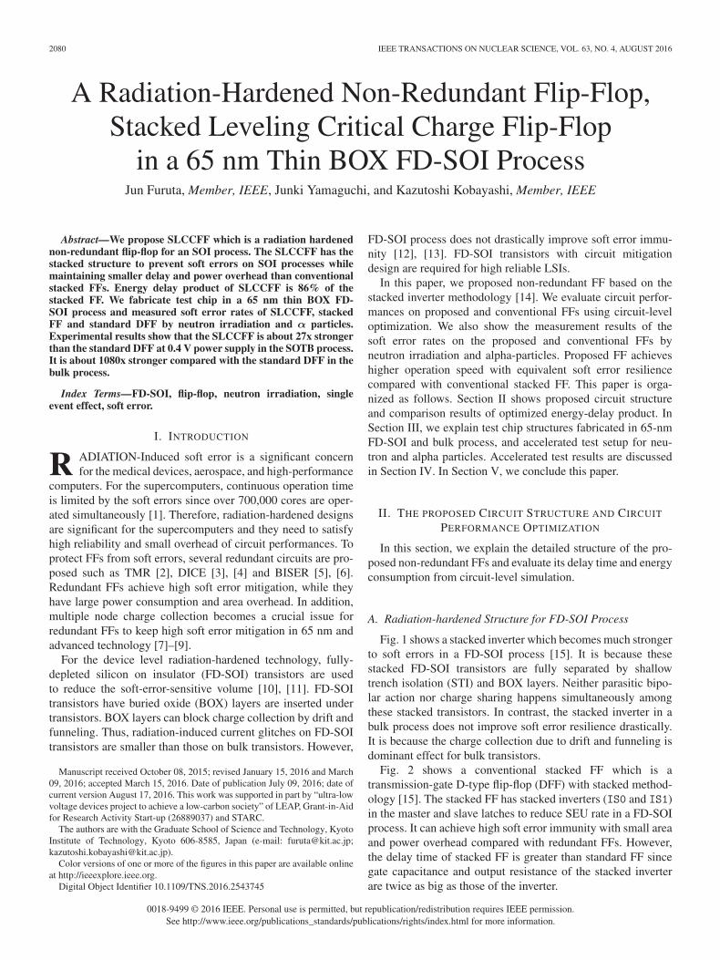
Fig. 5. Modified SLCCFF.
Fig. 6. Modified stacked FF.
Fig. 7. Optimization results of modified stacked FF and SLCCFF as shown inFig. 6 and Fig. 5. Energy and Delay values are normalized to those of DFF.
TABLE IIENERGY, DELAY, EDP, AND AREA OF MODIFIED STACKED FF AND
SLCCFF. ALL VALUES ARE NORMALIZED TO THOSE OF DFF
Modified stacked FF and SLCCFF are also optimized bydownhill simplex method. Fig. 7 and Table II shows optimiza-tion results. Compared with the stacked FF and SLCCFF inFig. 2 and Fig. 3, delay and energy overheads of modifiedstacked FF and SLCCFF are reduced. The modified SLCCFFachieves smaller delay time and energy consumption than thestacked FF. The ED product of the modified SLCCFF is 86% ofthe modified stacked FF
Fig. 8. Chip micrograph and floorplan.
Fig. 9. Transistor structure in the SOTB process.
III. ACCELERATED TEST SETUP BY SPALLATION
NEUTRON BEAM AND α PARTICLES
A. Test Chip Structure
In order to measure soft error rate by accelerated tests, testchips are fabricated in 65-nm bulk process and thin BOX FD-SOI processes which is named silicon-on-thin-BOX (SOTB)[18]. As shown in Fig. 9, the thicknesses of the BOX layer andbody layer are 10 and 12 nm, respectively. Fig. 8 shows a testchip micrograph with a floorplan. The layout designs of the testchips are strictly identical between SOTB and bulk processesexcept for BOX layers, while the channel impurity concentra-tions and threshold voltage of the SOTB transistors are lowerthan those of the bulk transistors [19]. Test chip has triple-wellstructure and well-contacts were inserted every 104 μm. TheFF-array part of a test chip is 1.3 mm × 5.0 mm and contains105,984 bit of DFFs, 99,360 bit of the unmodified stacked FFsand 185,472 bit of the unmodified SLCCFFs whose structuresare shown in Fig. 2 and Fig. 3, respectively. In the test chip, weimplement non-optimized stacked FFs and SLCCFFs as shownin Fig. 2 and Fig. 3. In addition, transistor sizes are not opti-mized in fabricated stacked FFs and SLCCFFs. It is becausesoft error rate (SER) may be changed by transistor sizes andwe focus on the difference of SERs caused by the connectionbetween stacked inverter and transmission gate. All FFs areconnected in series to form a shift register.
B. Experimental Setup
Accelerated tests by spallation neutron beam were performedat the research center for nuclear physics (RCNP), OsakaUniversity [20]. Fig. 10 shows the neutron beam spectrum incomparison with the terrestrial neutron spectrum at the groundlevel of New York. The average accelerated factor is about2.9× 108. Fig. 11 shows the test setup of the neutron irradi-ation. In order to increase the number of errors in the limitedmeasurement time, 16 test chips are measured simultaneously.
FURUTA et al.: A RADIATION-HARDENED NON-REDUNDANT FLIP-FLOP, STACKED LEVELING CRITICAL CHARGE FLIP-FLOP 2083
Fig. 10. Energy spectrum of spallation neutron beam normalized to that at theground level of NYC.
Fig. 11. Radiation test by the spallation neutron beam.
Fig. 12. Radiation test by α-particle irradiation.
Soft error rates induced by α-particle are measured by a 3 MBq 241Am source. Fig. 12 shows the test setup of the α-particleirradiation. The distance between the α source and the DUTis 0.7 mm. We measured soft error rates when master latches inFFs are hold state (clock signal, CLK is “1”). It is because beamtime is limited and the slave latches in stacked FF and SLCCFFhave the same structure as shown in Fig. 2 and Fig. 3. Therefore,we only changed stored values (Q) and supply voltage in thismeasurement.
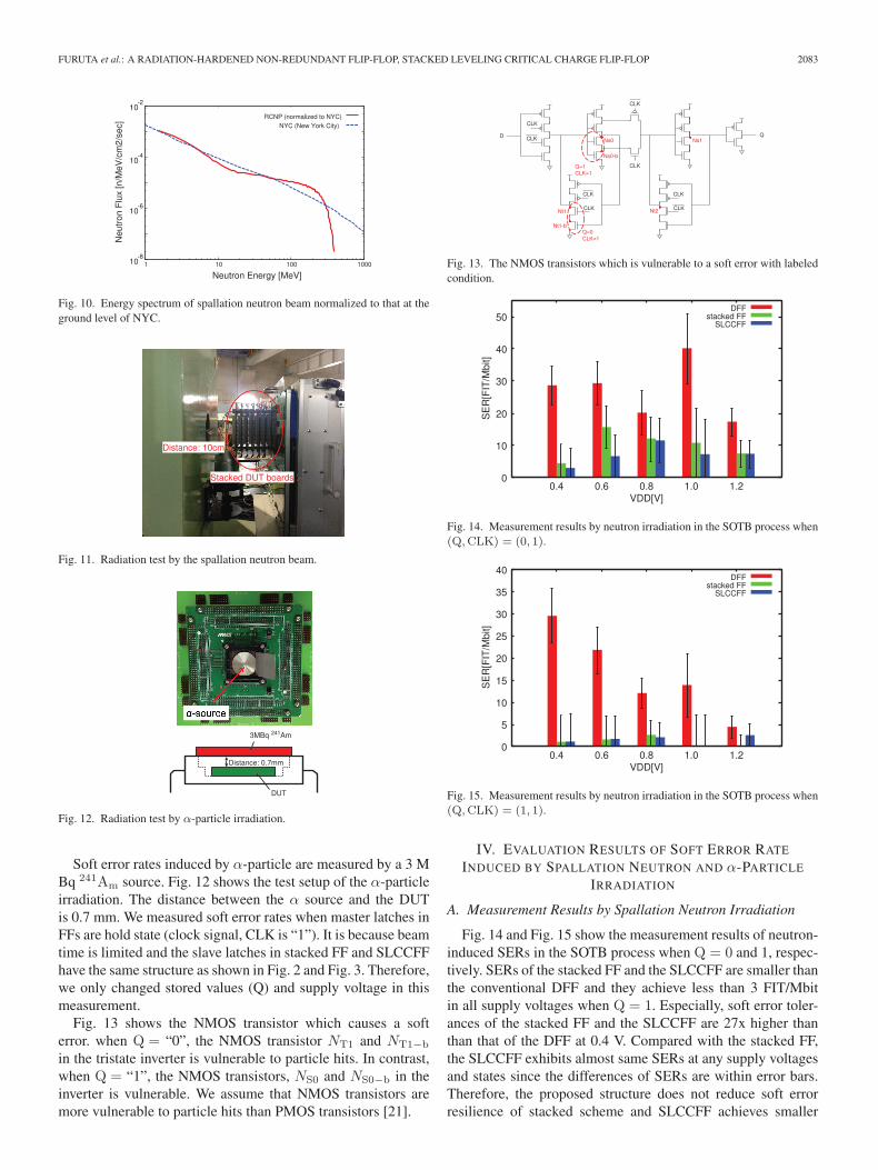
Fig. 13 shows the NMOS transistor which causes a softerror. when Q = “0”, the NMOS transistor NT1 and NT1−b
in the tristate inverter is vulnerable to particle hits. In contrast,when Q = “1”, the NMOS transistors, NS0 and NS0−b in theinverter is vulnerable. We assume that NMOS transistors aremore vulnerable to particle hits than PMOS transistors [21].
Fig. 13. The NMOS transistors which is vulnerable to a soft error with labeledcondition.
Fig. 14. Measurement results by neutron irradiation in the SOTB process when(Q,CLK) = (0, 1).
Fig. 15. Measurement results by neutron irradiation in the SOTB process when(Q,CLK) = (1, 1).
IV. EVALUATION RESULTS OF SOFT ERROR RATE
INDUCED BY SPALLATION NEUTRON AND α-PARTICLE
IRRADIATION
A. Measurement Results by Spallation Neutron Irradiation
Fig. 14 and Fig. 15 show the measurement results of neutron-induced SERs in the SOTB process when Q = 0 and 1, respec-tively. SERs of the stacked FF and the SLCCFF are smaller thanthe conventional DFF and they achieve less than 3 FIT/Mbitin all supply voltages when Q = 1. Especially, soft error toler-ances of the stacked FF and the SLCCFF are 27x higher thanthan that of the DFF at 0.4 V. Compared with the stacked FF,the SLCCFF exhibits almost same SERs at any supply voltagesand states since the differences of SERs are within error bars.Therefore, the proposed structure does not reduce soft errorresilience of stacked scheme and SLCCFF achieves smaller
2084 IEEE TRANSACTIONS ON NUCLEAR SCIENCE, VOL. 63, NO. 4, AUGUST 2016
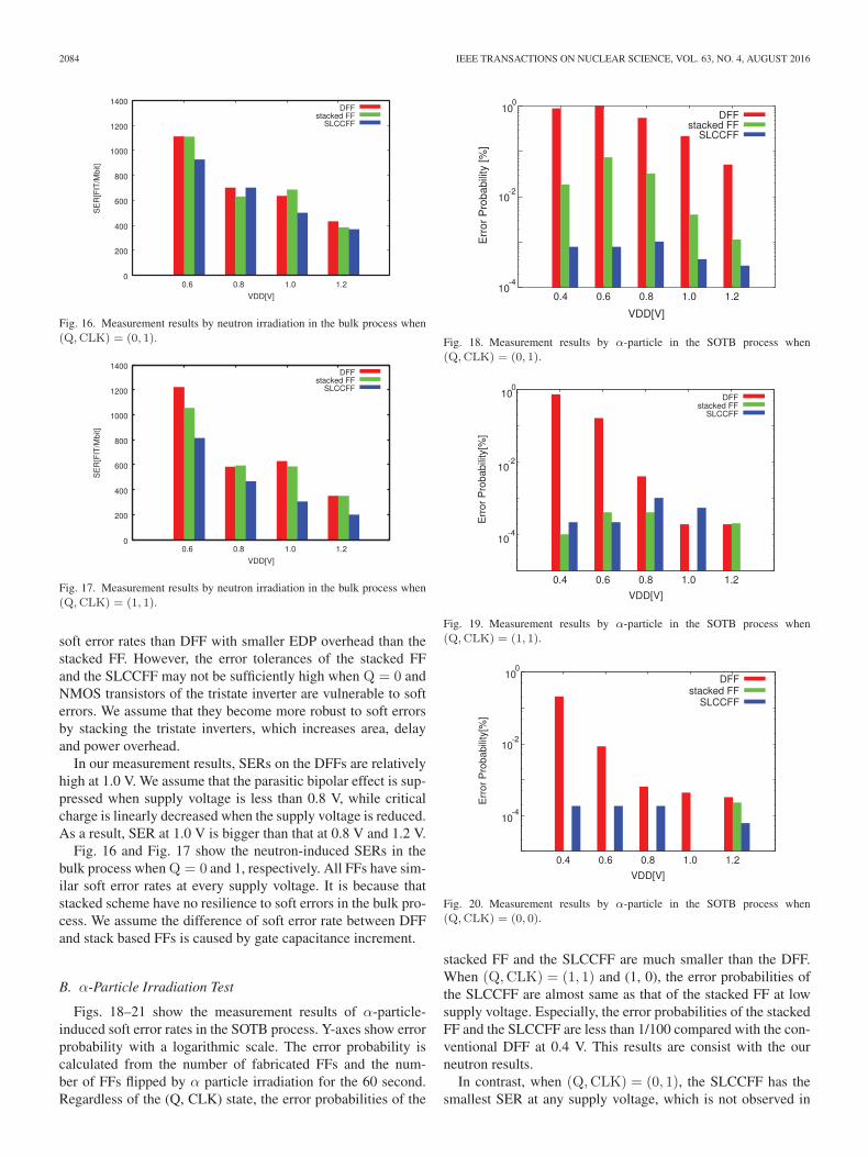
Fig. 16. Measurement results by neutron irradiation in the bulk process when(Q,CLK) = (0, 1).
Fig. 17. Measurement results by neutron irradiation in the bulk process when(Q,CLK) = (1, 1).
soft error rates than DFF with smaller EDP overhead than thestacked FF. However, the error tolerances of the stacked FFand the SLCCFF may not be sufficiently high when Q = 0 andNMOS transistors of the tristate inverter are vulnerable to softerrors. We assume that they become more robust to soft errorsby stacking the tristate inverters, which increases area, delayand power overhead.
In our measurement results, SERs on the DFFs are relativelyhigh at 1.0 V. We assume that the parasitic bipolar effect is sup-pressed when supply voltage is less than 0.8 V, while criticalcharge is linearly decreased when the supply voltage is reduced.As a result, SER at 1.0 V is bigger than that at 0.8 V and 1.2 V.
Fig. 16 and Fig. 17 show the neutron-induced SERs in thebulk process when Q = 0 and 1, respectively. All FFs have sim-ilar soft error rates at every supply voltage. It is because thatstacked scheme have no resilience to soft errors in the bulk pro-cess. We assume the difference of soft error rate between DFFand stack based FFs is caused by gate capacitance increment.
B. α-Particle Irradiation Test
Figs. 18–21 show the measurement results of α-particle-induced soft error rates in the SOTB process. Y-axes show errorprobability with a logarithmic scale. The error probability iscalculated from the number of fabricated FFs and the num-ber of FFs flipped by α particle irradiation for the 60 second.Regardless of the (Q, CLK) state, the error probabilities of the
Fig. 18. Measurement results by α-particle in the SOTB process when(Q,CLK) = (0, 1).
Fig. 19. Measurement results by α-particle in the SOTB process when(Q,CLK) = (1, 1).
Fig. 20. Measurement results by α-particle in the SOTB process when(Q,CLK) = (0, 0).
stacked FF and the SLCCFF are much smaller than the DFF.When (Q,CLK) = (1, 1) and (1, 0), the error probabilities ofthe SLCCFF are almost same as that of the stacked FF at lowsupply voltage. Especially, the error probabilities of the stackedFF and the SLCCFF are less than 1/100 compared with the con-ventional DFF at 0.4 V. This results are consist with the ourneutron results.
In contrast, when (Q,CLK) = (0, 1), the SLCCFF has thesmallest SER at any supply voltage, which is not observed in

FURUTA et al.: A RADIATION-HARDENED NON-REDUNDANT FLIP-FLOP, STACKED LEVELING CRITICAL CHARGE FLIP-FLOP 2085
Fig. 21. Measurement results by α-particle in the SOTB process when(Q,CLK) = (1, 0).
Fig. 22. Layout structures of stacked inverter IS0 and transmission gate TG inthe stacked FF and the SLCCFF. IS0 and TG are separated in the SLCCFF.
neutron-induced SER. When (Q,CLK) = (0, 1), it is conceiv-able that the NMOS transistor NT1 in the tristate inverter causesa soft error. However, the circuit structure of the tristate inverteris equivalent between the stacked FF and the SLCCFF. To eval-uate soft error rate, we calculate a critical charge of the NMOStransistor NT1 using single exponential current source [22]. Asingle exponential current source attached to the NMOS tran-sistor NT1. SPICE simulation results show the critical chargeof the stacked FF and SLCCFF are 1.4 fC and 1.0 fC at 0.4 V,respectively. As a result, the cause of the difference in thesoft error tolerance between stacked FF and SLCCFF when(Q,CLK) = (0, 1) does not observed in circuit-level simula-tion. We assume that the difference of SER might be causedby the difference of the layout structure between the stackedFF and the SLCCFF. Fig. 22 shows the layout structures of thestacked inverter IS0 and transmission gate TG in the stacked FFand the SLCCFF. In the SLCCFF, transmission gate is separatedfrom the stacked inverter. We assume that charge collection tomultiple nodes can be reduced in the SLCCFF. In addition,STI stress and transistor variation may increase and transis-tor performances are slightly changed. The difference of SERsbetween the stacked FF and the SLCCFF are clearly observedin alpha tests.
Fig. 23 and Fig. 24 shows the α-particle-induced SERs inthe bulk process. Y-axes show error probability with a linearscale. In the bulk process, α particle results show the samedependence as neutron results in any stored values.
Fig. 23. Measurement results by α-particle in the bulk process when(Q,CLK) = (0, 1).
Fig. 24. Measurement results by α-particle in the bulk process when(Q,CLK) = (1, 1).
TABLE IIIAVERAGE SERS OF THE DFF, THE STACKED FF AND THE SLCCFF
INDUCED BY NEUTRON AND α PARTICLES IN THE 65 NM SOTB PROCESS.SERS ARE NORMALIZED BY THOSE OF THE DFF AT 1.2 V
C. Soft Error Rate Comparison
Table III shows the average values of soft error rate whenQ = 0 and 1 in the 65 nm SOTB process. When supply voltageis 1.2 V, neutron-induced SER is not drastically decreased bythe stacked FFs. In contrast, neutron-induced SER is reducedto 9.2% (0.25 / 2.7) when supply voltage is 0.4 V. Thus, theSLCCFF and the stacked FF are used for sub-threshold opera-tion at the ground level. On the other hand, α-particle-inducedSERs of the stacked FF and the SLCCFF are ∼ 3% of SERs ofstandard DFF at any supply voltage. The SLCCFF have strongmitigation against lower LET radiation.
V. CONCLUSION
We propose non-redundant radiation hardened FF namedSLCCFF resilient to soft errors in the FD-SOI process for lowerenergy consumption and smaller delay than the conventionalstacked FF. The delay-energy product of the modified SLCCFFare 14% smaller than those of the modified stacked FF which isa non-redundant FF.
We also show accelerated test results on the stacked FF andthe SLCCFF which are not optimized in order to focus on
2086 IEEE TRANSACTIONS ON NUCLEAR SCIENCE, VOL. 63, NO. 4, AUGUST 2016
the difference of SERs due to the connection between stackedinverter and transmission gate. From the spallation neutron irra-diation, the SER of the unmodified SLCCFF is 1/27 of theconventional DFF on the 65 nm FD-SOI process. The unmod-ified SLCCFF achieve equivalent soft error mitigation to theunmodified stacked FF. In addition, from α-particle irradia-tion test, the error probability of the unmodified SLCCFF isless than 1/100 compared with conventional DFF in the SOTBprocess.
ACKNOWLEDGMENT
The authors would like to thank to Professors K. Hatanaka,M. Fukuda, and K. Takahisa of RCNP and all the other RCNPmembers for our neutron-beam experiments. The VLSI chipin this study was fabricated under the chip fabrication pro-gram of the VLSI Design and Education Center (VDEC), theUniversity of Tokyo in collaboration with Renesas ElectronicsCorporation, Cadence Corporation, Synopsys Corporation, andMentor Graphics Corporation.
REFERENCES
[1] H. Miyazaki et al., “K computer: 8.162 PetaFLOPS massively parallelscalar supercomputer built with over 548k cores,” Proc. IEEE Int. Solid-State Circuits Conf., Feb. 2012, pp. 192–194.
[2] L. Anghel, D. Alexandrescu, and M. Nicolaidis, “Evaluation of a softerror tolerance technique based on time and/or space redundancy,” Proc.Symp. Integr. Circuits and Syst. Des., Nov. 2000, pp. 237.
[3] D. Krueger, E. Francom, and J. Langsdorf, “Circuit design for voltagescaling and SER immunity on a quad-core itanium processor,” Proc. Int.Solid-State Circuits Conf., Feb. 2008, pp. 94–95.
[4] P. Hazucha et al., “Measurements and analysis of SER tolerant latch ina 90 nm dual-Vt CMOS process,” Proc. IEEE Custom Integr. CircuitsConf., Sep. 2003, pp. 617–620.
[5] S. Mitra, M. Zhang, S. Waqas, N. Seifert, B. Gill, and K. S. Kim,“Combinational logic soft error correction,” Proc. IEEE Int. Test Conf.,Oct. 2006, pp. 1–9.
[6] R. Yamamoto, C. Hamanaka, J. Furuta, K. Kobayashi, and H. Onodera,“An area-efficient 65 nm radiation-hard dual-modular flip-flop toavoid multiple cell upsets,” IEEE Trans. Nucl. Sci., vol. 58, no. 6,pp. 3053–3059, Dec. 2011.
[7] N. Seifert, B. Gill, K. Foley, and P. Relangi, “Multi-cell upset proba-bilities of 45 nm high-k + metal gate SRAM devices in terrestrial andspace environments,” Proc. IEEE Int. Rel. Physics Symp., Apr. 2008,pp. 181–186.
[8] S. Jagannathan, T. D. Loveless, Z. Diggins, B. L. Bhuva, S.-J. Wen,R. Wong, and L. W. Massengill, “Neutron- and alpha-particle inducedsoft-error rates for flip flops at a 40 nm technology node,” Proc. IEEEInt. Rel. Physics Symp., Apr. 2011, pp. SE.5.1–SE.5.5.
[9] J. Furuta, K. Kobayashi, and H. Onodera, “Impact of cell distance andwell-contact density on neutron-induced multiple cell upsets,” Proc.IEEE Int. Rel. Physics Symp., Apr. 2013, pp. 6C.3.1–6C.3.4.
[10] P. E. Dodd et al., “SEU-sensitive volumes in bulk and SOI SRAMs fromfirst-principles calculations and experiments,” IEEE Trans. Nucl. Sci.,vol. 48, no. 6, pp. 1893–1903, Dec. 2001.
[11] K. Hirose, H. Saito, Y. Kuroda, S. Ishii, Y. Fukuoka, and D. Takahashi,“SEU resistance in advanced SOI-SRAMs fabricated by commercialtechnology using a rad-hard circuit design,” IEEE Trans. Nucl. Sci.,vol. 49, no. 6, pp. 2965–2968, Dec. 2002.
[12] P. Roche, G. Gasiot, K. Forbes, V. O’Sullivan, and V. Ferlet,“Comparisons of soft error rate for SRAMs in commercial SOI and bulkbelow the 130-nm technology node,” IEEE Trans. Elec. Dev., vol. 50,no. 6, pp. 2046–2054, Dec. 2003.
[13] G. Gasiot, P. Roche, and P. Flatresse, “Comparison of multiple cell upsetresponse of bulk and soi 130 nm technologies in the terrestrial environ-ment,” Proc. IEEE Int. Rel. Physics Symp., Apr. 2008, pp. 192–194.
[14] J. Yamaguchi, J. Furuta, and K. Kobayashi, “A radiation-hardened non-redundant flip-flop, stacked leveling critical charge flip-flop in a 65 nmthin BOX FD-SOI process,” Proc. Conf. Radiation and its Effects onCompon. and Syst., Sep. 2015.
[15] A. Makihara et al., “Hardness-by-design approach for 0.15 μm fullydepleted CMOS/SOI digital logic devices with enhanced SEU/SETimmunity,” IEEE Trans. Nucl. Sci., vol. 52, no. 6, pp. 2524–2530, Dec.2005.
[16] R. John Koshel, “Enhancement of the downhill simplex method ofoptimization,” Proc. Int. Opt. Design Conf., Jun. 2002.
[17] V. Suzuki, K. Odagawa, and T. Abe, “Clocked CMOS calculator cir-cuitry,” IEEE J. Solid-State Circuits, vol. 8, no. 6, pp. 462–469, Dec.1973.
[18] Y. Morita et al., “Smallest Vth variability achieved by intrinsic siliconon thin BOX (SOTB) CMOS with single metal gate,” Proc. VLSI Tech.Symp., Jun. 2008, pp. 166–167.
[19] N. Sugii, R. Tsuchiya, T. Ishigaki, Y. Morita, H. Yoshimoto, andS. Kimura, “Local Vth variability and scalability in silicon-on-thin-BOX(SOTB) CMOS with small random-dopant fluctuation,” IEEE Trans.Electron Devices, vol. 57, no. 4, pp. 835–845, Apr. 2010.
[20] C. W. Slayman, “Theoretical correlation of broad spectrum neutronsources for accelerated soft error testing,” IEEE Trans. Electron Devices,vol. 57, no. 6, pp. 3163–3168, Dec. 2010.
[21] P. Hazucha et al., “Neutron soft error rate measurements in a 90-nmCMOS process and scaling trends in SRAM from 0.25 μm to 90-nmgeneration,” Proc. Int. Electron Device Meeting, 2003, pp. 523–526.
[22] P. Hazucha and C. Svensson, “Impact of CMOS technology scaling onthe atmospheric neutron soft error rate,” IEEE Trans. Nucl. Sci., vol. 47,no. 6, pp. 2586–2594, Dec. 2000.