ELD Institute Practicum Rigorous ELD Instruction Using Enhanced Into English! Lessons.

A programmable dark-field detector for imagingtwo-dimensional materials in the scanning electron
microscope
Benjamin W. Caplinsa, Jason D. Holma, and Robert R. Kellera
aNational Institute of Standards and Technology, 325 Broadway, Boulder, CO, USA 80305
ABSTRACT
Unit cell orientation information is encoded in electron diffraction patterns of crystalline materials. Traditionaltransmission electron detectors implemented in the scanning electron microscope are highly symmetric and areinsensitive to in-plane unit cell orientation information. Herein we detail the implementation of a transmissionelectron detector that utilizes a digital micromirror array to select anisotropic portions of a diffraction patternfor imaging purposes. We demonstrate that this detector can be used to map the in-plane orientation of grains intwo-dimensional materials. The described detector has the potential to replace and/or supplement conventionaltransmission electron detectors.
Keywords: digital micromirror device (DMD), scanning electron microscope (SEM), scanning transmissionelectron microscopy (STEM), transmission electron detector
1. INTRODUCTION
The scanning electron microscope (SEM) is widely used for imaging the surfaces of materials over six orders ofmagnitude in scale (10−3 m to 10−9 m).1 In an SEM, a focused electron beam (ca. 1 nm diameter on modernfield emission SEMs) is scanned across the surface of a bulk sample in a raster pattern. At each point on thesample, the electron beam interacts with the sample and generates a signal that is measured to create an image.By far, the most common signal measured to generate an image is known as the secondary electron (SE) signal,comprised of low-energy inelastic electrons, emitted in the backscatter direction. Generally, these electronsare collected over a large solid angle with an Everhart-Thornley detector2 and are relatively insensitive to thesample crystallography. When applied to 2D materials, SE images are generally used for their topographic,1
work function,3 or material-dependent SE-yield4 contrast mechanisms.
For nanomaterials in an SEM, where the electron mean free path at 30 keV can be comparable to the materialthickness, most of the incident electrons undergo small-angle scattering events and transmit through the sample(Figure 1a). This transmitted electron scattering distribution forms a diffraction pattern in the far-field, andportions of it can be detected to create real-space images. Experimental diffraction patterns of amorphous andcrystalline materials are shown in Figure 1b. In the SEM, transmission electron detectors are usually axiallysymmetric and integrate circular or annular regions of the diffraction pattern (e.g. Figure 1a). When the centraldisk of the diffraction pattern is spatially integrated, the corresponding image is called a ‘bright field’ (BF)image. Conversely, if some portion of the area outside the central disc is spatially integrated, the correspondingimage is called a ‘dark-field’ (DF) image. A common type of DF image is the annular dark-field (ADF) image.While these imaging modes enable mass-thickness measurements,1 they generally do not contain interpretablecrystallographic information in an SEM for 2D materials.
To obtain image contrast based on crystallographic orientation of 2D materials, a non-axially symmetricportion of the diffraction pattern needs to be integrated. As an example, we use the six-fold symmetric diffraction
*Contribution of NIST, an agency of the US government; not subject to copyright in the United States.Further author information: (Send correspondence to B.W.C.)B.W.C.: E-mail: [email protected].: E-mail: [email protected].: E-mail: [email protected]
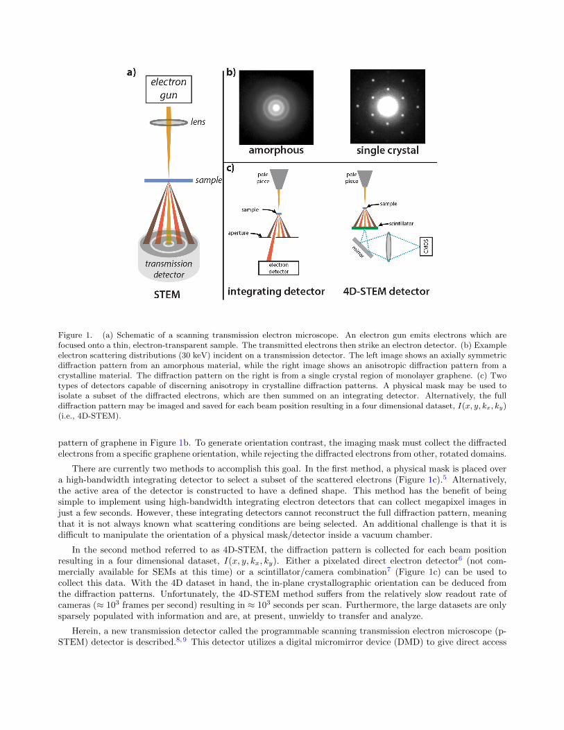
Figure 1. (a) Schematic of a scanning transmission electron microscope. An electron gun emits electrons which arefocused onto a thin, electron-transparent sample. The transmitted electrons then strike an electron detector. (b) Exampleelectron scattering distributions (30 keV) incident on a transmission detector. The left image shows an axially symmetricdiffraction pattern from an amorphous material, while the right image shows an anisotropic diffraction pattern from acrystalline material. The diffraction pattern on the right is from a single crystal region of monolayer graphene. (c) Twotypes of detectors capable of discerning anisotropy in crystalline diffraction patterns. A physical mask may be used toisolate a subset of the diffracted electrons, which are then summed on an integrating detector. Alternatively, the fulldiffraction pattern may be imaged and saved for each beam position resulting in a four dimensional dataset, I(x, y, kx, ky)(i.e., 4D-STEM).
pattern of graphene in Figure 1b. To generate orientation contrast, the imaging mask must collect the diffractedelectrons from a specific graphene orientation, while rejecting the diffracted electrons from other, rotated domains.
There are currently two methods to accomplish this goal. In the first method, a physical mask is placed overa high-bandwidth integrating detector to select a subset of the scattered electrons (Figure 1c).5 Alternatively,the active area of the detector is constructed to have a defined shape. This method has the benefit of beingsimple to implement using high-bandwidth integrating electron detectors that can collect megapixel images injust a few seconds. However, these integrating detectors cannot reconstruct the full diffraction pattern, meaningthat it is not always known what scattering conditions are being selected. An additional challenge is that it isdifficult to manipulate the orientation of a physical mask/detector inside a vacuum chamber.
In the second method referred to as 4D-STEM, the diffraction pattern is collected for each beam positionresulting in a four dimensional dataset, I(x, y, kx, ky). Either a pixelated direct electron detector6 (not com-mercially available for SEMs at this time) or a scintillator/camera combination7 (Figure 1c) can be used tocollect this data. With the 4D dataset in hand, the in-plane crystallographic orientation can be deduced fromthe diffraction patterns. Unfortunately, the 4D-STEM method suffers from the relatively slow readout rate ofcameras (≈ 103 frames per second) resulting in ≈ 103 seconds per scan. Furthermore, the large datasets are onlysparsely populated with information and are, at present, unwieldy to transfer and analyze.
Herein, a new transmission detector called the programmable scanning transmission electron microscope (p-STEM) detector is described.8,9 This detector utilizes a digital micromirror device (DMD) to give direct access
to the full electron diffraction pattern, with the additional capability to rapidly create targeted DF images, thatcan emphasize the crystallographic orientation of the sample. In many ways, this detector is a modern realizationof a detector suggested by Cowley and Spence in 1979, which used tiny mirrors on actuators in place of a DMD.10
As a proof of principle, we use the p-STEM detector to map the in-plane orientation of a graphene sample andgenerate diffraction contrast from multilayer graphene. To date, orientation mapping of graphene has not beendemonstrated with any other method in an SEM; this represents one of the most difficult samples to characterizedue to carbon’s low scattering cross section.11 To generate grain orientation maps of graphene, one could resortto performing conventional DF transmission electron microscopy (TEM).12,13 Due to DMD technology, however,we can perform this characterization in widely available and accessible SEMs.
2. DETECTOR CONSTRUCTION
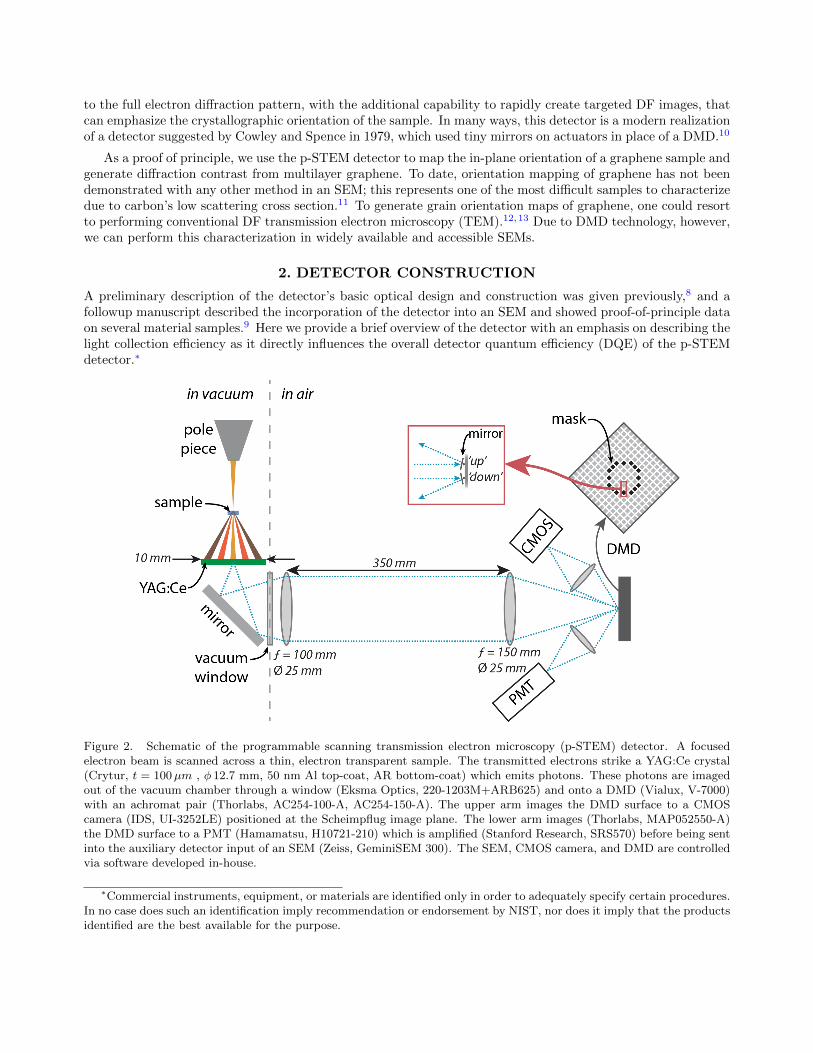
A preliminary description of the detector’s basic optical design and construction was given previously,8 and afollowup manuscript described the incorporation of the detector into an SEM and showed proof-of-principle dataon several material samples.9 Here we provide a brief overview of the detector with an emphasis on describing thelight collection efficiency as it directly influences the overall detector quantum efficiency (DQE) of the p-STEMdetector.∗
Figure 2. Schematic of the programmable scanning transmission electron microscopy (p-STEM) detector. A focusedelectron beam is scanned across a thin, electron transparent sample. The transmitted electrons strike a YAG:Ce crystal(Crytur, t = 100µm , φ 12.7 mm, 50 nm Al top-coat, AR bottom-coat) which emits photons. These photons are imagedout of the vacuum chamber through a window (Eksma Optics, 220-1203M+ARB625) and onto a DMD (Vialux, V-7000)with an achromat pair (Thorlabs, AC254-100-A, AC254-150-A). The upper arm images the DMD surface to a CMOScamera (IDS, UI-3252LE) positioned at the Scheimpflug image plane. The lower arm images (Thorlabs, MAP052550-A)the DMD surface to a PMT (Hamamatsu, H10721-210) which is amplified (Stanford Research, SRS570) before being sentinto the auxiliary detector input of an SEM (Zeiss, GeminiSEM 300). The SEM, CMOS camera, and DMD are controlledvia software developed in-house.
∗Commercial instruments, equipment, or materials are identified only in order to adequately specify certain procedures.In no case does such an identification imply recommendation or endorsement by NIST, nor does it imply that the productsidentified are the best available for the purpose.

2.1 Detector Hardware
The electron detector is constructed as shown in Figure 2 and can be separated into three parts: photongeneration, photon transport, and photon detection. Photons are generated when the transmitted electronsstrike a YAG:Ce scintillator crystal. Monte Carlo simulations (not shown) can provide insight into the photongeneration process.14 For example, simulations have shown that at a 30 keV beam energy, approximately 15 %of incident electron kinetic energy is lost due to electrons backscattered out of the scintillator. The remainingenergy is deposited on the order of 1µm deep into the scintillator material, far from the aluminum coating whichmight quench the excited Ce3+ ions. The conversion efficiency given for the YAG:Ce is 30 photons per keV(λ = 547 nm) which gives a yield of 765 photons per electron which we assume are isotropically emitted.
While the photon generation step has a large intrinsic gain, the photon transport from the scintillator to thedetector has a significant loss. The dominant loss is due to the small solid angle collected by the imaging optics.Only approximately 1 in 1000 photons is collected, which effectively cancels the gain of the electron generationstep. An electron transparent, optically reflective coating (50 nm of aluminum) on the top surface of the YAG:Cecrystal enhances the photon collection efficiency, while the reflective losses in the optical system slightly degradethe photon collection efficiency. In the final step, the photons are detected by a photomultiplier tube, which hasa low quantum efficiency (QE) at visible wavelengths. These steps and their relative gain/loss coefficients forthe detector configuration used here are given in Table 1.
Table 1. Steps in the photon generation, transport, and detection chain with calculated gain and loss coefficients. Thetotal efficiency is the product of all the coefficients.
step coefficient notes
deposition of energy into the scintillator 0.85 Loss due to electron backscattering estimatedfrom Monte Carlo simulation.14
energy to photon conversion 765 Assumes 30 photons (λ = 547 nm) generatedper 1 keV energy deposited with a 30 keVelectron beam. Value from manufacturer.15
increase in effective source intensity due toreflective coating
1.9 Assumes a 90 % reflectance from 50 nm Al.16
fraction of solid angle collected 9.7× 10⁻⁴ Assumes the φ 22.9 mm clear aperture of af = 100 mm lens is the limiting aperture.Includes the change in refractive index goingfrom YAG:Ce (n = 1.82) to air (n = 1).
reflective losses 0.9 Assumes 99 % transmission (reflectivity)from the various glass (mirror) surfaces.Lenses and vacuum window haveantireflective coatings.
loss from DMD 0.65 Includes DMD fill factor, reflectivity, windowtransmission, and diffraction efficiency asquoted by the DMD manufacturer.17
photomultiplier quantum efficiency (QE) 0.12 As quoted from PMT manufacturer.18
Combining the gain/loss coefficients, we calculate that for every electron that strikes the scintillator thereis a 8.4 % chance that it is detected, which gives a DQE of 0.078 assuming the detector has no noise sourcesother than counting statistics.19 Table 1 suggests there are two main routes to improve detector efficiency –the detector QE and the photon efficiency. First, the QE of the detector is 0.12, which leaves significant roomfor improvement. For example, a GaAsP PMT achieves ca. 40 % QE at 550 nm,20 though for some dark-fieldimaging applications the DQE could be degraded by the relatively high dark count rate of such detectors. Second,and most important, the collection efficiency of the optics is poor – on the order of 0.1 %. To improve this, largernumerical aperture lenses could be used, albeit at the expense of either increased aberration/distortion and/orreduced field of view.

Experimentally we estimated the probability of electron detection as 0.035 via a photon counting approach.Briefly, at a very low electron beam current the beam current is measured with a Faraday cup. Under effectivelyidentical conditions, the photon count rate was also measured. For low DQEs, the ratio of the photon countrate to electron beam current in electrons per second yields the average number of photons detected per electronincident on the scintillator. The dominant source of error arises from the the difficulty in detecting a photonevent in the PMT signal. By adjusting the photon detection criteria within a reasonable range, we estimate anuncertainty of at least to 20 % on the measured probability of electron detection.
The values in Table 1 result in an average photon yield approximately twice that of the photon countingmeasurement, though this is not unexpected. The calculation assumes the literature/manufacturer values areaccurate for the scintillator conversion efficiency and PMT QE, but theses values are known to vary from batchto batch, and the conditions under which they were determined are not specified. Additionally, the calculationassumes the optical system is perfectly aligned, which is likely not the case due to the difficulty of aligningan optical system with the physical constraints imposed by the vacuum chamber. In any case, the calculatedand measured detection probabilities are in qualitative agreement, suggesting that the limitations of the opticalassembly are understood. We note that we do not characterize the CMOS camera arm of the optical assembly,because the integration times for diffraction patterns are generally many orders of magnitude longer than thedwell times used for SEM image acquisition.
Finally, it is worth placing the DQE measurements/calculations in the context of an actual DF imagingexperiment in an SEM. The beam current on a field emission SEM is on the order of 300 pA which correspondsto 2× 10⁹ electrons per second. For monolayer graphene, a kinematic scattering calculation predicts ≈ 0.2 % ofthe beam will scatter into the 2nd order diffraction spots. For a DF image based on the 2nd order diffractionspots, the scattering efficiency, and the DQE, result in an electron detection rate of ca. 2.9 × 10⁵ electronsper second. This count-rate is notable for two reasons. First, the PMT selected for the p-STEM detector hasa dark count rate several orders of magnitude below this expected signal, and thus should not add additionalnoise. Second, because of the high contrast intrinsic to DF images, a 1 megapixel DF image should be able tobe acquired on the order of minutes with a signal to noise in excess of the Rose criterion. In this manuscript,integration times for single DF images were ≤ 120 s, in reasonable agreement with this estimate.
2.2 Detector Software
To utilize the p-STEM detector in an experiment, software was developed to control the SEM, the DMD, and thetwo optical detectors (PMT and CMOS camera) simultaneously. Two main modes were developed. In ‘diffractionmode’ the user can load an SEM micrograph into a graphical user interface (GUI) and select several regionsof the sample from which to collect diffraction patterns. In this mode, the program tilts all the micromirrorstowards the CMOS camera, positions the electron beam at the locations on the sample specified by the user, andthen collects and saves the diffraction patterns. These diffraction patterns are then corrected for optical imagingdistortions using an affine transform and presented to the user.
In ‘imaging mode’, the user loads in diffraction patterns from regions on their sample. Then using the GUI,the user can create various digital masks to apply to the DMD which will serve as a digital ‘objective aperture’ tocollect bright and dark field images of the sample. The types of masks that are currently included in the GUI arecircular, annular, two dimensional lattices, user selected spots, and combinations thereof. More complex maskscan be generated via external scripts. Once the user has specified a diffraction mask, the mask is mapped to theDMD image plane and applied to the DMD. The user can then collect images with the SEM software using theoutput of the PMT as the signal source. Further details on the method of mapping the diffraction images andmasks to different image planes is given in a previous manuscript.9
3. APPLICATIONS OF THE DETECTOR TO GRAPHENE
3.1 Orientation Contrast in Monolayer Graphene
As a proof-of-principle we use graphene samples on a lacey carbon support (Ted Pella, 21710) to show orientation-based contrast with the p-STEM detector. These films consist of continuous, mostly flat monolayer grapheneacross the TEM grid with small patches of bilayers. Folds and wrinkles of the graphene are also present. Coating

Figure 3. This figure shows how the p-STEM detector can yield orientation contrast from graphene samples that istotally absent from conventional SEM imaging modes. All real-space images are from the same field-of-view. (a) A SEimage of a monolayer graphene sample. (b) An ADF image. Neither of these ‘conventional’ SEM imaging modes showany measurable orientation contrast from the graphene – they only show debris on the graphene surface. (c,d) Diffractionpatterns from the two locations specified in (a). The two diffraction patterns are rotated 23◦ with respect to one another.(e,f) DF images collected by masking the diffraction patterns as shown in (c,d).
the graphene films is a mixture of amorphous (polymer leftover from a transfer step) and crystalline (assumedto be leftover salts from the etching and lift-off process) materials.
Figure 3 shows conventional SEM imaging modes in addition to diffraction contrast images made possibleby the p-STEM detector. Figure 3a is an SE image taken with a conventional Everhart-Thornley detector, andFigure 3b is an ADF image taken with an annulus that is set to accept the signal from (transmitted) electronsdiffracted by the graphene lattice. Both images show similar features, though the ADF image has greater signalto noise. The small dark patches are likely clean graphene, while the grey texture that coats the surface isassigned as adsorbed organic – likely polymer residue.21 The small bright spots (≈ 10 nm) are crystalline debris.
Figure 3c-d show diffraction patterns collected in ‘diffraction mode’ at locations I and II as specified in Figure3a. The diffraction patterns show two main features. First, they show the first three diffraction orders fromgraphene as spots (the 3rd order is extremely weak as expected). The relative intensity of the 1st and 2nd orderdiffraction spots was measured to be close to 1 and indicates that the graphene is monolayer thickness.22 Thetwo diffraction patterns show a 23◦ relative orientation. Second, low intensity diffuse rings are visible near the1st and 2nd order diffraction spots. These rings are due to the amorphous debris coating the sample. Prolongedexposure to the electron beam will increase these diffuse rings via electron-beam-induced sample contamination.
Figure 3e-f show DF images collected by creating two different DF masks that collect the diffraction spotsof each diffraction pattern in Figure 3c-d. In these images, there is a clear contrast between the left and rightsides of the field of view separated by a distinct interface. This interface is a grain boundary, and the spatialresolution is limited only by that of the SEM image. We note that this interface is not visible in conventional

Figure 4. This figure shows how the p-STEM detector can perform orientation mapping of graphene. (a) A DF maskis designed to overlap with the 1st and 2nd order graphene diffraction spots over a finite angular range of the in-planeorientation angle, φ. A series of 30 such masks are generated for φ ∈ {0◦, 2◦, 4◦...58◦} and a DF image is collected foreach mask. From this stack of images, an orientation map can be constructed and is displayed in (b). Here the laceycarbon is colored black, and holes in the graphene sheet are colored white. Several grains with different orientation areobvious in the field of view.
SEM imaging modes (BF, ADF, SE) regardless of the image processing steps taken. The data show that thep-STEM detector is capable of obtaining image contrast not available with conventional SEM imaging modes.
Once this diffraction contrast is observed, it is relatively straightforward to develop an automated method formapping the orientation of graphene domains. Here, a series of digital masks is generated that has the symmetryof the graphene diffraction pattern, but with each mask having a different in-plane orientation parameterizedby φ (Figure 4a). By generating a series of these masks that span the angular range φ ∈ [0◦, 60◦] and collectinga DF image for each mask, we can determine the orientation of the graphene lattice at each pixel. Figure 4bshows an orientation map with several grains of graphene visible. To obtain high quality orientation maps,we performed rigid image registration to account for sample drift.23 Additionally, the data in Figure 4b wasfiltered with a total variational denoising algorithm on each DF image prior to computing the orientation. Totalvariation denosing significantly reduces the noise in piecewise constant images without smoothing the edges (i.e.grain boundaries).24 In the present work, we used a first circular moment analysis of the image stack to obtainthe graphene orientation.25 More advanced peak finding or pattern matching methods26 would likely be moreaccurate at an increased computational cost.
3.2 Orientation Contrast in Bilayer Graphene
In addition to mapping the orientation contrast in monolayer graphene films, this detector can be used to mapthe orientation in bilayer films. Figure 5a shows a SE image of a graphene film. Diffraction patterns werecollected at location I and II as indicated and are shown in Figure 5b-c respectively. Location II shows only asingle orientation of graphene, while location I shows a two orientations of graphene. Three DF images werecollected corresponding to the masks shown. The DF image corresponding to the dotted blue mask in Figure 5brepresents a background image due to electrons scattered from the surface debris and lacey carbon. Figure 5e-fcorrespond to the two DF masks that each collected the electrons scattered from a particular graphene latticeorientation. The data show that there is an annular shaped island of graphene on top of a continuous graphenesheet.
3.3 Moire Fringe Contrast in Multilayer Graphene
Multiple layers of graphene with nearly the same orientation will give rise to moire fringes/patterns in DF images.If visible, these periodic signals give insight into the local stacking of graphene multilayers. Figure 6a shows adiffraction pattern collected from a multilayer region of graphene. Three DF images were collected (Figure 6b-d)using the three diffraction spots specified. In all three DF images, moire fringes are readily visible signifyingstrain and/or misorientation between the layers.27
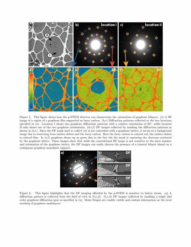
Figure 5. This figure shows how the p-STEM detector can characterize the orientation of graphene bilayers. (a) A SEimage of a region of a graphene film supported on lacey carbon. (b,c) Diffraction patterns collected at the two locationsspecified in (a). Location I shows two graphene diffraction patterns with a relative orientation of 30◦, while locationII only shows one of the two graphene orientations. (d,e,f) DF images collected by masking the diffraction patterns asshown in (b,c). Since the DF mask used to collect (d) is not coincident with a graphene lattice, it serves as a backgroundimage due to scattering from surface debris and the lacey carbon. Here the lacey carbon is colored red, the surface debrisis colored blue. In (e,f) graphene shows up as green due to the fact the the mask is capturing the electrons scatteredby the graphene lattice. These images show that while the conventional SE image is not sensitive to the layer numberand orientation of the graphene lattice, the DF images can easily discern the presence of a rotated bilayer island on acontiguous graphene monolayer support.
Figure 6. This figure highlights that the DF imaging afforded by the p-STEM is sensitive to lattice strain. (a) Adiffraction pattern is collected from the field of view in (b,c,d). (b,c,d) DF images collected by masking a single 2ndorder graphene diffraction spot as specified in (a). Moire fringes are readily visible and contain information on the localstacking of graphene multilayers.
4. CONCLUSIONS
Traditional imaging modes in an SEM have limited sensitivity to the crystallographic orientation of 2D materials.Herein, crystallographic contrast was not observed on monolayer graphene when using an Everhart ThornleySE detector or a BF or ADF transmission electron detector. The basic problem is that orientational contrastrequires a non-axially symmetric detector capable of differentiating in-plane rotations. One method to constructa detector sensitive to in-plane orientation uses a DMD in an image plane conjugate to the diffraction pattern toserve as a programmable DF mask. By incorporating DMD technology into the p-STEM detector, we are ableto switch between ‘imaging’ and ‘diffraction’ modes without any macroscopic moving parts. This allows the userto perform all DF masking operations digitally. We demonstrate that the p-STEM detector has the potentialto characterize grain orientation in 2D materials. We believe that DMD technology will enable the SEM to beused to investigate phenomena that previously required the use of a TEM.
ACKNOWLEDGMENTS
We thank Ryan White (NIST) and Ann Chiaramonti Debay (NIST) for helpful microscopy related discussions,and Callie Higgins (NIST) for discussions related to optics. This work was performed while B.W.C. held a Na-tional Research Council Postdoctoral Associateship. The authors also thank the NIST Small Business InnovationResearch Program for supporting RadiaBeam Technologies’ detector development under Contract SB1341-14-CN-0026.
REFERENCES
[1] Goldstein, J. I., Newbury, D. E., Echlin, P., Joy, D. C., Lyman, C. E., Lifshin, E., Sawyer, L., and Michael,J. R., [Scanning Electron Microscopy and X-ray Microanalysis ], Springer US, Boston, MA (2003).
[2] Everhart, T. E. and Thornley, R. F. M., “Wide-band detector for micro-microampere low-energy electroncurrents,” Journal of Scientific Instruments 37, 246–248 (jul 1960).
[3] Zhou, Y., Fox, D. S., Maguire, P., O’Connell, R., Masters, R., Rodenburg, C., Wu, H., Dapor, M., Chen,Y., and Zhang, H., “Quantitative secondary electron imaging for work function extraction at atomic leveland layer identification of graphene,” Scientific Reports 6, 21045 (aug 2016).
[4] Yoo, Y., Degregorio, Z. P., and Johns, J. E., “Seed Crystal Homogeneity Controls Lateral and VerticalHeteroepitaxy of Monolayer MoS2and WS2,” Journal of the American Chemical Society 137(45), 14281–14287 (2015).
[5] Holm, J. and Keller, R. R., “Angularly-selective transmission imaging in a scanning electron microscope,”Ultramicroscopy 167, 43–56 (aug 2016).
[6] Faruqi, A. and McMullan, G., “Direct imaging detectors for electron microscopy,” Nuclear Instrumentsand Methods in Physics Research Section A: Accelerators, Spectrometers, Detectors and Associated Equip-ment 878, 180–190 (jan 2018).
[7] Fundenberger, J. J., Bouzy, E., Goran, D., Guyon, J., Yuan, H., and Morawiec, A., “Orientation mappingby transmission-SEM with an on-axis detector,” Ultramicroscopy 161, 17–22 (2016).
[8] Jacobson, B. T., Gavryushkin, D., Harrison, M., and Woods, K., “Angularly sensitive detector for trans-mission Kikuchi diffraction in a scanning electron microscope,” Proceedings of SPIE of SPIE 9376(310),93760K (2015).
[9] Caplins, B. W., Holm, J. D., and Keller, R. R., “Transmission imaging with a programmable detector in ascanning electron microscope,” Ultramicroscopy 196, 40–48 (jan 2019).
[10] Cowley, J. and Spence, J., “Innovative imaging and microdiffraction in stem,” Ultramicroscopy 3, 433–438(jan 1978).
[11] Reimer, L., [Scanning Electron Microscopy ], vol. 45 of Springer Series in Optical Sciences, Springer BerlinHeidelberg, Berlin, Heidelberg (1998).
[12] Kim, K., Lee, Z., Regan, W., Kisielowski, C., Crommie, M. F., and Zettl, A., “Grain Boundary Mappingin Polycrystalline Graphene,” ACS Nano 5, 2142–2146 (mar 2011).
[13] Huang, P. Y., Ruiz-Vargas, C. S., van der Zande, A. M., Whitney, W. S., Levendorf, M. P., Kevek, J. W.,Garg, S., Alden, J. S., Hustedt, C. J., Zhu, Y., Park, J., McEuen, P. L., and Muller, D. A., “Grains andgrain boundaries in single-layer graphene atomic patchwork quilts,” Nature 469, 389–392 (jan 2011).
[14] Demers, H., Poirier-Demers, N., Couture, A. R., Joly, D., Guilmain, M., De Jonge, N., and Drouin,D., “Three-dimensional electron microscopy simulation with the CASINO Monte Carlo software,” Scan-ning 33(3), 135–146 (2011).
[15] CRYTUR, “YAG:Ce Technical Parameters.”
[16] Hass, G. and Waylonis, J. E., “Optical Constants and Reflectance and Transmittance of Evaporated Alu-minum in the Visible and Ultraviolet,” Journal of the Optical Society of America 51, 719 (jul 1961).
[17] Instruments, T., “DLP7000 Technical Documents.”
[18] Hamamatsu, “Photosensor module: H10721-210.”
[19] Browne, M. and Ward, J., “Detectors for stem, and the measurement of their detective quantum efficiency,”Ultramicroscopy 7, 249–262 (jan 1982).
[20] Thorlabs, “PMT2101 - GaAsP Amplified PMT.”
[21] Dyck, O., Kim, S., Kalinin, S. V., and Jesse, S., “Mitigating e-beam-induced hydrocarbon deposition ongraphene for atomic-scale scanning transmission electron microscopy studies,” Journal of Vacuum Science& Technology B, Nanotechnology and Microelectronics: Materials, Processing, Measurement, and Phenom-ena 36, 011801 (jan 2018).
[22] Shevitski, B., Mecklenburg, M., Hubbard, W. A., White, E. R., Dawson, B., Lodge, M. S., Ishigami, M.,and Regan, B. C., “Dark-field transmission electron microscopy and the Debye-Waller factor of graphene,”Physical Review B 87, 045417 (jan 2013).
[23] Guizar-Sicairos, M., Thurman, S. T., and Fienup, J. R., “Efficient subpixel image registration algorithms,”Optics Letters 33, 156 (jan 2008).
[24] Rudin, L. I., Osher, S., and Fatemi, E., “Nonlinear total variation based noise removal algorithms,” PhysicaD: Nonlinear Phenomena 60, 259–268 (nov 1992).
[25] Mardia, K. V. and Jupp, P. E., eds., [Directional Statistics ], Wiley Series in Probability and Statistics, JohnWiley & Sons, Inc., Hoboken, NJ, USA (jan 1999).
[26] Chen, Y. H., Park, S. U., Wei, D., Newstadt, G., Jackson, M. A., Simmons, J. P., De Graef, M., and Hero,A. O., “A Dictionary Approach to Electron Backscatter Diffraction Indexing,” Microscopy and Microanal-ysis 21, 739–752 (jun 2015).
[27] Brown, L., Hovden, R., Huang, P., Wojcik, M., Muller, D. A., and Park, J., “Twinning and Twisting ofTri- and Bilayer Graphene,” Nano Letters 12, 1609–1615 (mar 2012).