Voltage Reference - From Diode to High Precision High Order BandGap
1014 IEEE JOURNAL OF SOLID-STATE CIRCUITS, VOL. SC-19, NO. 6, DECEMBER 1984
A Precision CMOS Bandgap Reference
JOHN MICHEJDA AND SUK K. KIM
Abstract — This paper describes the design of a precision on-chip band-
gap voltage reference for applications with CMOS analog circuits. The
circuit uses naturally occurring vertical n-p-n bipolar transistors as refer-
ence diodes. P-tub diffusions are nsed as temperature-dependent resistors
to provide current bias, and an op-amp is used for voltage gain. The circuit
is simple. Only two reference diodes, three p-tub resistors, and one op-amp
are necessary to produce a reference with fixed voltage of – 1.3 V. An
additional op-amp with two p-tnb resistors will adjust the output to any
desired value.
The criteria for temperature compensation are presented and show that
the properly compensated circuit can in principle produce thermal drift
which is less than 10 ppm/” C. Process sensitivity analysis shows that in
practical applications it is possible to control the output to better’ than 2
percent, while keeping thermal drift below 40 ppm/°C. Test circuits have
been designed and fabricated. The output voltage produced was – 1.30 ~
0.025 V with thermal drift less than 7 mV from 0° C to 125° C. Significant
improvements in performance, at modest cost in circuit complexity, can be
achieved if the op-amp offset contribution to the output voltage is reduced
or eliminated.
I. INTRODUCTION
I N a large and complex LSI-CMOS analog circuit, the
voltage reference is often a potentially most troublesome
component since it must produce a temperature stable,
process invariant, and precisely controlled output. In the
past, most of efforts in voltage reference design have
emphasized temperature compensation at the expense of
output precision. The commonly used references based on
the difference between gate/source voltages of enhance-
ment and depletion mode MOS transistors realize low
thermal drift; however, the absolute magnitude of output is
poorly controlled because it depends on the accuracy of
depletion and enhancement implants [1]. In the bandgap
references, where the output is derived from the voltage
difference of two diodes forward biased by ratioed cur-
rents, both the thermal drift and the absolute value of the
output can be controlled with precision [2]–[4].
A CIVfOS bandgap voltage reference which uses bipolar-
like source-to-drain transfer characteristics of MOS tran-
sistor in weak inversion was reported [5], [6]. The output
voltage exhibited relatively low thermal drift and tight
voltage spread from sample to sample. Another approach
[7] used precision curvature-compensated switched capaci-
tor CMOS bandgap reference. It required trimming and
used a complex circuitry for generation of bias currents,
thus consuming a large area.
Manuscnpt receivedAugust 12, 1983; revisedJuly 13, 1984.J. M1chejda is with AT&T Bell Laboratories, Murray HI1l, NJ 07974.S. K. Kim is with Solid State Electronics Division, Honeywell, MN
55441.
This paper describes the design of another simple band-
gap circuit that can be conveniently implemented in CMOS
technology. The output of this circuit is both temperature
stable and precise. The circuit configuration which follows
that given by Kuijk [8] uses temperature dependent p-tub
resistors to provide bias currents to the reference diodes,
which are the emitter-base junctions of the bipolar tran-
sistors formed by the n+ diffusion inside the p-tub. First,
the basic circuit and the criteria for temperature compensa-
tion are presented, followed by discussion of the character-
istics of the reference diodes and biasing resistors. The
sensitivity of the output voltage to the most common
process variation, and the power supply fluctuations will
then be discussed in detail. Finally, the experimental re-
sults to verify circuit performance will be presented to
illustrate the precision and the stability of the circuit.
H. THE BANDGAP CIRCUIT
In the bandgap circuit the output voltage is derived from
the voltage difference across two identical diodes forward-
biased by two unequal, precisely ratioed currents. The
positive temperature coefficient of this difference is then
cancelled by the negative temperature coefficient of voltage
across one of the diodes. If the voltage across diode 1 is
Vl( 7’) and across diode 2 is V2(T), then the output can be
expressed as
vout=A(vl(T)- v2(T))+B(v2(T))
=avl(T)–bv2(T) (1)
where constants a and b are chosen to obtain a voltage VOut
that has a minimum variation over the temperature range
of interest.
The principles of bandgap references and the criteria for
derivation of constants a and b are given in detail in [4].
These are derived for devices biased by either temperature
independent constant current 1, or currents which vary
with temperature as T“, where a is a constant. Neither one
of these temperature variations of currents can be easily
implemented in a CMOS analog circuit.
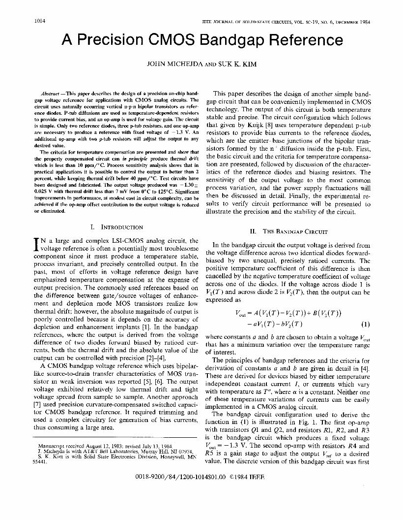
The bandgap circuit configuration used to derive the
function in (1) is illustrated in Fig. 1. The first op-amp
with transistors Q1 and Q2, and resistors Rl, R 2, and R 3is the bandgap circuit which produces a fixed voltage
VOut= – 1.3 V. The second op-amp with resistors R4 and
R5 is a gain stage to adjust the output V,ef to a desired
value. The discrete version of this bandgap circuit was first
0018-9200/84/1200-1014$01.00 01984 IEEE
MICHFJDA AND KIM: PRSCISION CMOS BANDGAP REFERENCE 1015
‘DD The voltage drop at temperature T is given byT T
Fig. :1. Schematic of the CMOS bandgap circuit to produce negativeoutput voltage. A bandgap source developing positive output withrespect to ground is illustrated in [9].
proposed by Kuijk [8], who used integrated diode pairs and
thin film resistors. More recently, Ye and Tsividis [9] have
demonstrated this configuration, and a configuration pro-
ducing a positive output voltage, using vertical n-p-n bi-
polar transistors and discrete external resistors. They also
suggested using diffusion or polysilicon resistors in a fully
integrated version of this circuit.
The gain constants a and b of circuit in Fig. 1 are given
by
a= R3/R2 i-l (2)
Inl addition to the gain of the circuit, which is de-
termined by the ratio of resistors R ~ and R ~, the magni-
tude and the ratio of the bias currents is determined by the
ratio of resistors RI and R ~:
‘(T)=n[vG(T’+(?)ln(*)‘7)where n is the nonideality factor, VG(T ) is the bandgap
voltage at temperature T, k is the Boltzmann constant, q is
the electron charge, A is a normalizing constant related
to the geometry of the device, and ~ is a constant related
to the fabrication process.
VG(T) is itself a function of temperature. Reference [10]
gives the empirical expression for the bandgap value ex-
trapolated from physical measurement over temperattnx?
range from 300 to 400 K.
dVGVG(T)=VGO+~T ($)
where VGO=1.20595 V, and dVG/dT = – 2.7325X 10⁻⁴V/K.
For a circuit whose function is given by (l), subject to
the condition that the temperature coefficient at tempera-
ture T = TO is zero,
dYOut
dT ~.~,= o. (9)
The value of the output voltage VOut(TO)is unique and
given by
[() kTOvout(To)=n VGO+ —
q
VOU,–Vi(T)II(T)= R
1(4) (B-l+T”(ZHH=O))’10)
VOut–Vi(T) _ VOut– V(T)12(T)= R – R +; . (5)
3 3 2
In this implementation, however, the biasing currents
II(T) and 12(T) are temperature dependent because of the
variation of VI(T) and V2(T ), and to a lesser extent
becaluse of the variation of VOutwith respect to tempera-
ture, The conditions for the temperature compensation of
this circuit with temperature independent RI, R z, and R ~are {&en in [8].
In CMOS technology the situation is even further com-
plicated because the orIly on-chip conductors that have
large enough resistance values for proper biasing of the
reference diodes are also temperature-dependent. The p-tub
where dR /dT I~= TOis the derivative of resistance of bias-
ing resistors with respect to temperature at TO.The temperature response to the bandgap equation can
be described by th~ following differential equation:
T dVOut
--vo~t+%lwdT
+ +W+”vgo=o. (11)
It is important to notice that the value of VOut(TO)as given
in (10), and the bandgap temperature response as given in
(11) depends only on physical diode parameters n and ~,
and resistor temperature coefficient (1/R )(dR/dT).
resistors approximately double their resistance for a tern-
- perature in;reaie from- O to 100”C.
‘” Tlhe detailed derivation of the temperature compensationIII. THE REFERENCE DIODE IN A CMOS BANDGAP
for the circuit illustrated in Fig. 1 is algebraically tediusCIRCUIT
and is briefly summarized in this section. It is well known that nearly ideal diode characteristicsFor a reference diode whose current 1 is given by can be obtained from the base–emitter voltage V~e of a
Shockley’s equation, for qV >> nkT, bipolar transistor. In the twin tub CMOS technology the
I = Ioeqvlnk=.vertical n-p-n bipolar devices are readily available with n –
(6) substrate collector, p-tub base, and n+ emitter.
1016 IEEE JOURNAL OF SOLID-STATE CIRCUITS, VOL. SC-19, NO. 6, DECEMBER 1984
In the layout of the bipolar devices five unit transistors
are connected in parallel to make one reference diode. In
this approach, similar to the one given in [6], the reference
device can operate at larger biasing current, and in ad-
dition better matching of references can be achieved.
These devices, each unit transistor with 20 pm X 20 pm
emitter, manufactured in the 3.5 pm linear twin tub CMOS
process, were characterized to obtain the value of parame-
ters n and ~ necessary to predict the voltage drop across
the reference device as given in (7).
The value of n was determined by measuring 1– V
characteristics of the reference devices at room temperature
between currents of 0.5 and 500 PA, and then fitting the
measured voltage using (7), with n being the adjustable
parameter. The voltage drop of the diode in the fit was
normalized to the value at the lowest current. The best fit
was obtained for n = 1.01 over a range of currents from 0.5
to 25 pA. At currents above 25 p A, the differences be-
tween measured voltage and the fit were greater than 0.5
mV.
To measure the ~ parameter directly, the precise 1– V
characteristics of reference devices over a wide range of
temperatures are needed. Such a measurement is tedious
and difficult to do precisely, because a minor inaccuracy
(as little as 0.5°C) in temperature measurement of the
references, can lead to large errors in estimate of ~. When
these measurements are made on devices placed on a wafer
prober, an uncertainty in temperature between the thermo-
couple in the wafer chuck, and the wafer itself can also
cause significant errors in the value of ~.
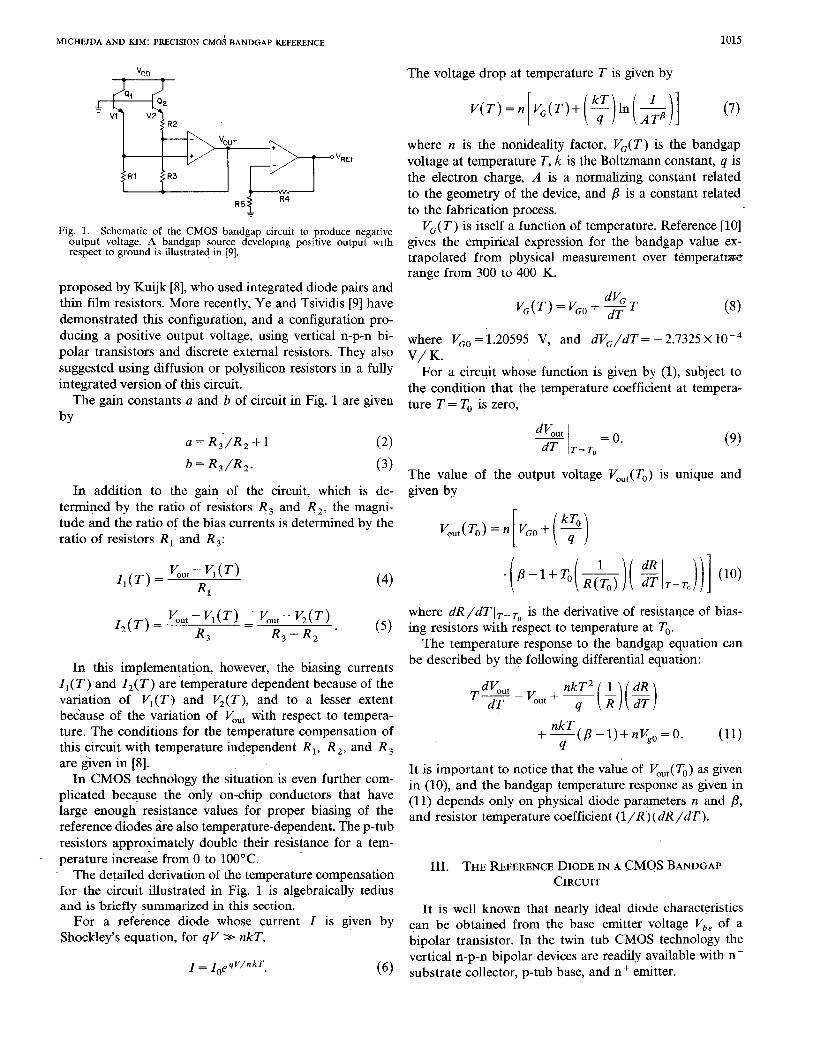
A new indirect method of measurement was used in
determining the value ~. A precision op-amp with low
input offset and high open-loop gain, and a set of precision
discrete resistors whose values were individually measured,
were externally connected to the bipolar devices on the
wafer. The connections were identical to those of the
bandgap circuit, and the values of discrete resistors were
selected ‘to minimize the output variations with tempera-
ture. The voltage produced by the circuit was measured as
a function of temperature of the reference diodes. A fit to
the data as a function of ~ was made using the computer
simulation of the bandgap circuit. Fig. 2 illustrates the
measured and predicted responses of the circuit. The best
overall agreement is for ~ =1.775.
The simulator used to obtain the best fit was written in
Fortran. The program contains appropriate diode modelsgiven in (7), and (8), to generate the 1– V– T characteristics
of the reference diodes. Given diode characteristics, and
the resistance values RI, R ~, and R ~, the program solves
iteratively for bias points VI and V2, and output voltage
V& until,
VOU,-V1(R1(T), T) _ VOU,–V2(R3(T), T) R~(T)
RI(T) – R2(T)+R3(T) “ RI(T) “
(12)
-4284
-1 :s88 -
–4.290 -
-1.292 -
-1 :?94 - - MEASUREMENT
--- @ =1.800
--- p .,,~~~
- ?.298 -—x— ~ =4.750
–– ~ =4,725
-1.298 - p ,4,700
I.,,,00 ~
80 80 100 120
TEMPERATURE (UC)
Fig. 2. Comparison of temperature response between simulated andmeasured fi:~ed resistor bandgap circuit to determine the vatue of ,8.
This method of measurement is much less sensitive to
vagaries in temperature meas~rement since the discrete
resistors are chosen to minimize temperature dependence
of the output voltage. This decreased output voltage sensi-
tivity to temperature enables easier, and more precise
determination of ~.
IV. BIASING RESISTORS IN THE CMOS BANDGAP
CIRCUIT
The results of the diode characterizations described in
the previous section illustrate that the proper operation of
reference devices requires small biasing currents in the
microampere range. To provide these small currents, resis-
tance values of the order of 105 Q or higher are needed.
The only on-chip conductor available in CMOS technology
that has sufficiently high sheet resistance to render these
resistors practical is the p-tub diffusion. The sheet resis-
tance of the p-tub diffusion in the 3.5 ~m twin tub CMOS
technology is -3 kfl/U. Thus, resistor values up to 0.5
MQ can be readily realized.
P-tub resistors exhibit temperature dependent behavior
due to mobility changes over the temperature range of
interest. The measurements of temperature effect on mobil-
ity variation of ‘p-type silicon samples [11] yielded mobility
dependence of T-22. The measurements of temperature
dependence of p-tub resistance, illustrated in Fig. 3, yielded
essentially the same result.
Therefore, for a p-tub resistor,
R(T) =ROT22 (13)

MICEIEJDA AND KIM: PRECISION CMOS BANDGAP REFERENCE 1017
100 -
90 -
80 –
70 – R,
60 –
50 -R2
40 -
30 - — R=ROT22
I . MEASUREMENTS
I~o,,lnT(”K)
Fig. 3. Temperature characteristic of the p-tub resistors.
where R ~ is the normalizing constant. Therefore,
[l\(dR} 2.2(14)
and the proper compensation, according to formula (10),
occurs when I&t at TO is
[ (3P++ (H)‘out(~O) ‘~ ‘GO+
Fig. 4 illustrates the predicted temperature response of
the bandgap circuit from O to 100”C, where the resistance
of biasing resistors varies as T22, the value of /3 =1.775,
and the value of To is 50°C. The value of VOUt( To) is– 1.3018 V, and the temperature variation of P& over
100°C is approximately 1 mV. The temperature coefficient
that can be obtained using this approach is less than 8
pprn/°C.
V. PROCESS SENSITIVITY OF THE OUTPUT VOLTAGE
One of the advantages of the bandgap references over
the threshold differencing scheme is that both magnitude
ancl temperature compensation of the output voltage are
relatively tolerant of processing variations. In this section
an approximate analysis of the sensitivity of the output
volltage to the processing variants will be presented. The
current density ratio between reference diodes is 25:1
yielding voltage differenc~ (Vl - Vz) -80 mV at 25°C. The
value of constants a and b in (1) is 10 and 9, respectively.
The main processing parameters that affect the output of
the bandgap circuit are: p-tub doping, resistor mismatch,
reference diode mismatch, and the threshold mismatch of
the op-amp input devices. The threshold mismatch, which
results in the op-amp offset error, mainly affects the mag-
nitude of the output voltage if the offset itself is not a
function of temperature. All other processing variations
affect magnitude, as well as the temperature compensation
of the output.
-1,3006
-4,3008
-13010
p
6z -1.?-912
‘5
>0
-1.3044
-1.3016
-1.30180 20 40 60 80 +00
TEMF3SRATURE (“C)
Fig. 4. Predicted temperature response of the bandgap circuit.
The doping of the p-tub affects the resistance of the
biasing resistors and the P’be drop across the reference
diodes. Both the value of the biasing resistors, and the Vbe
drop across the reference devices affect the voltages VI apd
V2 of the circuit.
The resistance of the p-tub resistor uniformly doped by
ion implantation is inversely proportional to tbe implant
dose of boron lV,.
(16)
Therefore, for a fractional error in implant dose dN,/iV,,the fractional error on the p-tub resistance dR/R is;
dR – dN$—-—RN, ”
(17)
For the n-p-n bipolar device biased with fixed V~G, the
collector current is proportional to the number of impuri-
ties/unit area in the base [12] (also known as Gurnmel
number). For the device with ion implanted p-tub base,
this number is equal to the iop implant dose N,. Therefore,
I-h ~qvh,/kT (18)s
and the Vbedrop across the reference device is
V -~ln(lN~).be (19)
The change in Vb~ of the reference device due to the
p-tub ion implant error is
kT dN,dVbe = — —
qN~”(20)
The doping of the p-tub in the twin tub CMOS process
can be controlled to + 10 percent. This variation in the ion

1018 IEEE JOURNAL OF SOLID-STATE CIRCUITS, VOL. SC-19, NO. 6, DECEMBER 1984
implant dose should result in a + 0.1 kT, or + 2.5 mV
error in Vbe at room temperature.
From (19) the variation of the voltage across the refer-
ence device biased by the p-tub resistor resulting from the
changes in V~, and the bias current is
[1kT dN dIdV1=dV2=y @+F
s(21)
For bias current 1 in the circuit,
V&t – VbgI=
R’(22)
the change in current dI is
dVOut– dVbedI= ~ –
(%, - %) dR
R2(23)
for 10% resistance variation, the first term in (23) is small.
Therefore.dl dR—~__I R
and using (17), (21), and (24)
(12kT dN,dV1=dV2=— —
9%”
(24)
(25)
The bandgap output voltage change is then
dVOutl= adV1 - bdV, = (a - b) dV1 = dV1. (26)
The total variation of the output voltage due to variation in
the p-tub doping is
(27)
The +10 percent error in the p-tub implant will result in
+ 5 mV error in the output voltage at room temperature.
This is significantly better than the accuracy of the ~utput
voltage produced by the threshold differencing circuit due
to the Ion implant variation.
The V&e voltage produced by the reference devices isvery uniform, ‘and the mismatch of the voltage across
different devices of the same size on the same chip is small.
The measurements of the reference devices biased with
constant current on the different chip sites of the same
wafer yielded the mafimum mismatch of less than 0.2 mV.
Such a mismatch would result in a output voltage changeof
dVOut2= adV1 = bdV2 = 2 mV (28)
where the value of a =10 is used.
The mismatch of the resistor ratio R3 and R ~ affects the
gain of the circuit. The mismatch of the ratio RI and R3influences the current ratio supplied to the references, and
thus the difference between VI and V2.The resistances RI and R ~ can be matched accurately
because they can be ratioed by an exact integer factor, and
-“”~
. A ;~g .
-x-x-_x-x-x
-x-x -x —x—x —x-x-x-~-x-x
~-------------------- . ------ ------- --------- ---
d . . . . . . . ...00.0........0...00...0.. . . . . . . . . . . . ...”
s>0 . . . . . . . . . . . . . . . . . . . . . . . . . . . . . . . . . . . . . . . . . . . . . . ● .”
----------------- -------- ----------- -------- . ..-.
x-x-xkx-x--1:31 - x-x-x-x_ x—x-x-x-x-x-x-
.,,),~0 20 40 60 60 100
TEMPERATURE [°C)
— NOMINAL RESPGNSE
. . . . . OIOOE MISMATCH ! 0,2MV
---- P-TUB IMPLANT ERROR MO%
- X- RESISTOR RATlo MISMATCH tt OA
— TOTAL VARIATION OUE TO ABOVE ERRORS
Fig. 5, Sensitivity of output voltage to processing variations
also because RI and R ~ have an identic~ voltage across
them thus eliminating problems due to any nonlinearities
of p-tub resistance. The mismatch of R ~ and R ~ is more
likely to occur since these resistors are ratioed by a nonin-
teger number, and because R z is biased at a differentpotential from the substrate than RI and R ~. Therefore,
only R ~/l?., mismatch will be considered here.
The variation of the output voltage of the bandgap
circuit due tc) mismatch of R ~, and R z is
‘Vo.t=d(%++l-d(%,=d(a(v-(29)
In a careful layout the resistance values of the p-tub
resistors can be matched better than 1 percent. Therefore,
for 1 percent resistance mismatching and 80 mV difference
between VI and V2, with R, /R z = 10 the output voltage
error is
dVOut3H
=0.01 # (V1– V2)=8mV. (30)2,
The above discussion illustrated that excluding the offset
error of the op-amp the various processing variations can
affect the oultput voltage of the bandgap circuit by about
+ 15” mV at room temperature in the worst-case analysis.
This @ only about 1.2 percent of the total voltage produced
by the bandgap circuit. The estimate of the effect of these
parameters on temperature compensation is considerably
more difficult and was done using the numerical bandgap
simulator discussed in Section III. Fig. 5 illustrates the
predicted worst-case behavior of the bandgap circuit and
how each prclcessing variation contributes to errors in the
output voltage temperature compensation.
MICHEJDA AND JSJM: PRSCISION CMOS BANDGAP REFERENCE 1019
In this simulation the output of each reference diode
voltage was varied by + 2.5 mV, reference device mismatch
was varied by + 0.2’ mV, the sheet resistivity of biasing
resistors was varied by ~ 10 percent and the ratio of
resistors was mismatched by ~ 1 percent. The worst-case
analysis yields the temperature compensation of the output
voltage of about 5 mV over the temperature range from O
to 100”C.The input offset error of the summing op-amp can have
significant and detrimental effect on the control of the
magnitude of the output voltage. An analysis of the band-
gap circuit shown in Fig. 1, which includes the offset error
of the op-amp, gives the following relation for J&t.
P&t = UP-I– bv2 + Cvo, (31)
where a and b are given in (2) and (3), VO, is the offset,
and
(ic=– 1+5 =.a
Rz “(32)
The offset of the op-amp is therefore multiplied by the
factor c. In a typical bandgap circuit, c =10; thus, small
offset value of the op-amp can contribute a large error to
the output voltage.
VI. SENSITIVITY OF OUTPUT VOLTAGE TO POWER
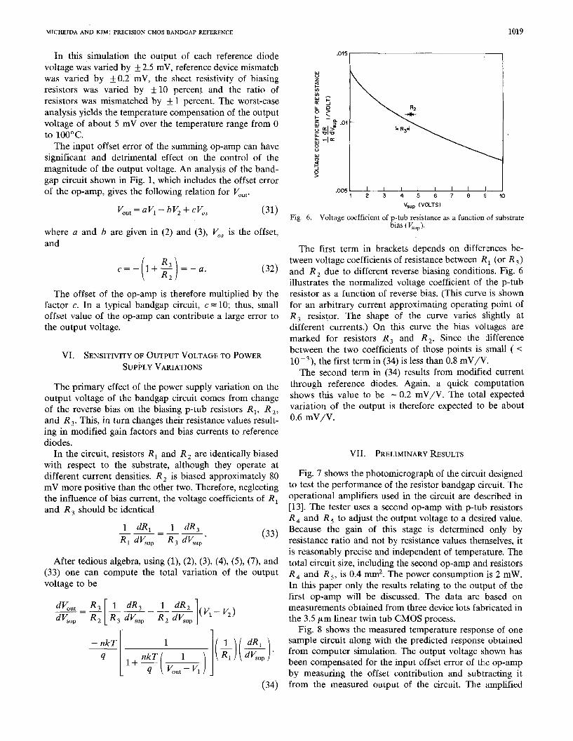
SUPPLY VARIATIONS
The primary effect of the power supply variation on the
output voltage of the bandgap circuit comes from change
of the reverse bias on the biasing p-tub resistors RI, R ~,and R ~. This, in turn changes their resistance values result-
ing in modified gain factors and bias currents to reference
diodes.
In the circuit, resistors RI and R ~ are identically biased
with respect to the substrate, although they operate at
different current densities. Rj is biased approximately 80
mV more positive than the other two. Therefore, neglecting
the influence of bias current, the voltage coefficients of RIand R ~ should be identical
(33)
After tedious algebra, using (l), (2), (3), (4), (5), (7), and
(33) one can compute the total variation of the output
voltage to be
-[-
dVOut R3 1 dR3
dV& = 1:2 # (VI- V,)—— —
Rz R3 d<up sup
r 1
(34)
““”r 1
.. . I—L—l.— ~J1234567 8910
V~up (VOLTS)
Fig. 6. Voltage coefficient of p-tub resistance as a function of substratebias ( ~u~).
The first term in brackets depends on differences be-
tween voltage coefficients of resistance between RI (or R ~)and R ~ due to different reverse biasing conditions. Fig. 6
illustrates the normalized voltage coefficient of the p-tub
resistor as a function of reverse bias. (This curve is shown
for an arbitrary current approximating operating point of
R ~ resistor. The shape of the curve varies slightly at
different currents.) On this curve the bias voltages are
marked for resistors R ~ and R z. Since the difference
between the two coefficients of those points is small ( -=
10- 3), the first term in (34) is less than 0.8 mV/V”.
The second term in (34) results from modified current
through reference diodes. Again, a quick computation
shows this value to be -0.2 mV/V. The total expected
variation of the output is therefore expected to be about
0.6 mV/V.
VII. PRELIMINARY RESULTS
Fig. 7 shows the photomicrograph of the circuii designed
to test the performance of the resistor bandgap circuit. The
operational amplifiers used in the circuit are de~;cribed in
[13]. The tester uses a second op-amp with p-tub resistors
R ~ and R ~ to adjust the output voltage to a desired value.
Because the gain of this stage is determined only by
resistance ratio and not by resistance values themselves, it
is reasonably precise and independent of temperature. The
total circuit size, including the second op-amp and resistors
R ~ and R5, is 0.4 mm2. The power consumption is 2 mW.
In this paper only the results relating to the output of the
first op-amp will be discussed. The data are based on
measurements obtained from three device lots fabricated in
the 3.5 pm linear twin tub CMOS process.
Fig. 8 shows the measured temperature resporlse of one
sample circuit along with the predicted response obtained
from computer simulation. The output voltage shown has
been compensated for the input offset error of th,e op-amp
by measuring the offset contribution and subtracting it
from the measured output of the circuit. The amplified
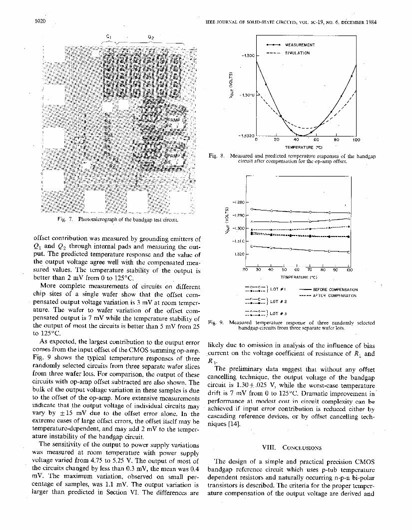
1020 IEEE JOURNAL OF SOLID-STATE CIRCUITS, VOL. SC-19, NO. 6, DECEMBER 1984
QI
q~ — MEASUREMENT
-1.300 –---- SIMULATION
p
“. , ...”..d~
1->2
,- f.3oto –1 \
\\
,.. \\\
\
. ., “. “.,.,.
-!.:3020 I
o 20 40 60 80 100
TEMPERATURE (°C).,.
Fig. 8. Measured and predicted temperature responses of the bandgap
,, circuit after compensation for the op-amp offset.
,...”,,.,.
,,, .:,.$, ,, f.. . .;.’,.’ .:’ ,,.::.”,. -1.280 –
... , , ,“” ,, 0,. ., “. . ... “:. ,, ..
~i.. , o~ —0
~ -IZ90 -—0— 0
Fig. 7. Photomicrograph of the bandgap test circuit. > —Aa— A_ A—A— A
5 -1,300–>0
----------------------------~------------------
n:=:==-_--=~r= . . . ..* . . . . . . . ..—...---*
offset contribution was measured by grounding emitters of -! 310–Q, and Q2 through internal pads and measuring the out- ❑—n—n
put. The predicted temperature response and the value of 1.320–—0——0
the output voltage agree well with the compensated mea- 1 I I I I I I Isured values. The temperature stability of the output is 20304050 !wT0 80901m
better than 2 mV from O to 125”C.TEMPERATURE (“C)
More complete measurements of circuits on different ~~~~~) LOT #l
\
— BEFCRE COMPENSATION
chip sites of a single wafer show that the offset com- ----- AFTER COMPENSATION
pensated output voltage variation is 3 mV at room temper- ~~~”~} LOT # 2
ature. The wafer to wafer variation of the offset com- n~.zfn) LOT # 3
pensated output is 7 mV while the temperature stability of
the output of most the circuits is better than 5 mV from 25Fig. 9. Measured temperature response of three randomly selected
bandgap circuits from threeseparatewafer lots.
to 125°C.
As expected, the largest contribution to the output error likely due to omission in analysis of the influence of biascomes from the input offset of the CMOS summing op-amp. ‘current on t]he voltage coefficient of resistance of RI and
Fig. 9 shows the typical temperature responses of three R ~-
randomly selected circuits from three separate wafer slices The preliminary data suggest that without any offsetfrom three wafer lots. For comparison, the output of these ~ancellingte&niquq the output voltage of the bandgap
circuits with op-amp offset subtracted are also shown. The
bulk of the output voltage variation in these samples is duecircuit is 1.30 ~ .025 V, while the worst-case temperature
drift is 7 mV from O to 125 ‘C. Dramatic improvement into the offset of the op-amp. More extensive measurementsindicate that the output voltage of individual circuits may
performance at modest cost in circuit complexity can beachieved if input error contribution is reduced either by
vary by ~ 15 mV due to the offset error alone. In the cascading reference devices, or by offset canceling tech-extreme cases of large offset errors, the offset itself may be niques [14].temperature-dependent, and may add 2 mV to the temper-
ature instability of the bandgap circuit.
The sensitivity of the output to power supply variations VIII. CONCLUSIONSwas measured at room temperature with power supply
voltage varied from 4.75 to 5.25 V. The output of most of The design of a simple and practical precision CMOS
the circuits changed by less than 0.3 mV, the mean was 0.4 bandgap reference circuit which uses p-tub temperature
mV. The maximum variation, observed on small per- dependent resistors and naturally occurring n-p-n hi-polar
centage of samples, was 1.1 mV. The output variation is transistors is described. The criteria for the proper temper-
Iarger than predicted in Section VI. The differences are ature compelmsation of the output voltage are derived and
MICHEJDA AND KIM: PRSCISION CMOS BANDGAP REFERENCE
are shown to be independent of the design parameters such
as current values and their ratios, resistor values, or diode
bias points. The diodes manufactured in the 3.5 ~m twin
tub linear CMOS process are shown to be acceptable for
the references in the bandgap circuit. The magnitude and
tem~perature stability of the output voltage is shown to be
tolerant to the most common variations of the CMOS
process. The performance of the test circuits matches well
the predictions of the bandgap response made by the
ban.dgap computer simulations. The output voltage of the
circuit is – 1.30 ~ .025 V with temperature stability better
than 7 mV from O to 125 “C. A version of this circuit,
which produces positive output is shown in [9]. A dramatic
improvement in the performance can be achieved if op-amp
offset error contribution is reduced by using offset cor-
recting techniques.
ACKNOWLEDGMENT
The authors wish to acknowledge the support offered by
H. J. Boll and J. G. Ruth, and to Y. P. Tsividis for many
fruitful discussions. They are thankful to P. B. Smalley for
performing the testing.
[1]
[2]
[3]
[4]
[5]
[6]
[7]
[8]
[9]
.WFER13NCEs
R. A. Blauschild, P. A. Tucci, R. S. Muller, and R. G. Meyer, “Anew NMOS temperature-stable voltage reference,” IEEE J. Solid-State Circuits, vol. SC-13, pp. 767-774, Dec. 1978.R. J. Widlar, “New developments in IC voltage regulators,” IEEEJ. Solid-State Circuit~, vol. SC-6, pp. 2-7, Feb. 1971.A. P. Brokaw, “A simple three-terminat IC bandgap reference,”IEEE J. Solid-State Circuits, vol. SC-9, pp. 388–393? Dec. 1974.P. R. Gray and R. G. Meyer, Analysis and Design of AnafogIntegrated Circuits. New York: Wiley, 1977.E. Vittoz and O. Neyrund, “A low voltage CMOS bandgap refer-ence,” IEEE J. Solid-State Circuits, vol. SC-14, June 1979.E. Vittoz, “ MOS transistors operated in the lateral bipolar modeand their application in CMOS technology,” IEEE J. Solid-StateCircuits, vol. SC-18, June 1983.B. S. Song and P. R. Gray, “A precision curvature-compensatedCMOS bandgap reference,” in ISSCC Dig. Tech. Papers, vol. 26,Feb. 1983, pp. 240–241.K. Kuijk, “A precision referencevoltage source;’ IEEE J. Solid-State Circuits, vol. SC-8, pp. 222-226, June 1973.R. Ye and Y. Tsividis, “ Bandgap voltage reference sources inCMOS technology,” Electron. Lett., vol. 18, no. 1, pp. 24–25, Jan.1982.
[10]
[11]
[12]
[13]
[14]
1021
Y. P. Tsividis, “Accurate anafysis of temperature effects in IC– V~,characteristics with applications to bandgap reference devices,”IEEE J. Solid-State Circuits, vol. SC-15, pp. 1076-1084, Dec. 1980.C. Jacobini et al., “A review of some charge transport properties ofsilicon,” Solid-State Electron., VOL 20, P. 77, 1977.S. M. Sze, Physics of Semicortductor ~evices, 2nd ed. New York:Wiley, 1981.V. R. Saari, “Low-power high-drive CMOS operational amplifiers,”IEEE J. So/id-State Circuits, vol. SC-18, pp. 121-127, Feb. 1983.K. C. Hsiech and P. R. Gray, “A low-noise chopper-stabilizeddifferential switched-capacitor filtering technique;’ in LSSCC Dig.Tech. Papers, vol. 24, Feb. 1981, pp. 128-179.
John Michejda was born in Wroclaw, Poland, in1950. He received the B.E. degree in eruineeringscience from State University of New York, Ston~Brook, in 1972, and Ph.D. in engineering andapplied science from Yafe University, NewHaven, CT, in 1977.
In 1977 he joined Bell Labs, Allentown, PA,where he worked in memory processing and de-sign groups. In 1980 he joined VLSI Group, BellLabs, Murray Hill, NJ, where he was engaged indesign of a very high-speed digitaf signaf proc-
essor using 1 pm fine-line NMOS technology. He is currently Supervisorof the High Speed Digital Design Group in charge of digital circuits forhigh bit rate opticaf communication systems.
Murrav Hill, NJ. where
Suk K. Kim was born in Sok-cho, Korea. Hereceived the B.S. and M.S. degrees in electricalengineering from Korea University, Seoul, Korea,in 1973 and 1975, respectively, and the M.S. andPh.D. degrees in electrical engineering from theUniversity of Minnesota, Minneapolis, MN, in1979 and 1980, respectively.
After completing the first M.S. degree in 1975,he worked as a Process Engineer at the KoreaInstitute of Science and Technology, Seoul,Korea, for one year. In 1980 he joined Bell Labs,he was a Linear CMOS Designer ~articir)atinz in.,. -L.
voltage reference development, op-amp design, and the latest genera~onof linear CMOS circuit design. Since 1983 he has been with Honeywelf’sSolid-State Electronics Division, Plymouth, MN, and involved in develop-ing a very fast A/D converter, an ultra low noise amplifier, a voltagereference, and a very high impedance sensor amplifier all in CMOStechnology.