A Physically Based, Scalable MOS and Extraction...
18
TM A Physically Based, Scalable MOS Varactor Model and Extraction Methodology for RF Applications James Victory 1 , Zhixin Yan 1 , Gennady Gildenblat 2 , Colin McAndrew 3 , Jie Zheng 1 1 Jazz Semiconductor, Newport Beach, CA 2 Pennsylvania State University, State College, PA 3 Freescale Semiconductor, Tempe, AZ , USA
Transcript of A Physically Based, Scalable MOS and Extraction...
TM
A Physically Based, Scalable MOS Varactor Model
and Extraction Methodology for RF
Applications
James Victory1, Zhixin Yan1, Gennady Gildenblat2, Colin McAndrew3, Jie Zheng1
1 Jazz Semiconductor, Newport Beach, CA 2 Pennsylvania State University, State College, PA
3 Freescale Semiconductor, Tempe, AZ , USA

2
InnovationManufactured
MOS-AK 2005
Outline
• Introduction
• Frequency Dependent Analytical Surface Potential Based MOS Capacitance Model (Implemented in VerilogA)
• MOS Varactor Model (Implemented in VerilogA)
• Physical Parameter Extraction
• Model Verification
• Conclusions

3
InnovationManufactured
MOS-AK 2005
Introduction (1)
• MOS Varactor Modeling Prior Art:
– Force MOSFET model, BSIM usually the choice, to emulate MOS capacitor
• Float source and drain to force deep depletion
• Kinks in accumulation-depletion interface, heart of CV tuning in varactor
– Polynomial CV equations, no physical basis
– Reasonable models for parasitics*
– Verification over limited geometry, most papers show only 1 geometry• No emphasis on extraction
– ReferencesK. Molnar, G. Rappitsch, Z. Huszka, and E. Seebacher, “MOS Varactor Modeling With a Subcircuit Utilizing the BSIM3v3 Model”, IEEE Trans. Electron Devices, vol. 49, no. 7, pp. 1206-1211, July 2002
C. Geng, K. S. Yeo, K. W. Chew, J. Ma, and M. A. Do, “A Simple Unified Scaleable RF Model for Accumulation-Mode Varactor”, Proc. 2000 ICDA
*S. Song and H. Shin, “An RF Model of the Accumulation-Mode MOS Varactor Valid in Both Accumu-lation and Depletion Regions”, IEEE Trans. Electron Devices, vol. 50, no. 9, pp. 1997-1999 , September 2003

4
InnovationManufactured
MOS-AK 2005
Introduction (2)
• Key things to get right:
– Physical CV equation dependent on process and geometry parameters to allow accurate statistical modeling
• Cmax/Cmin, tuning range variation with geometry
• Accurate dC/dV critical for VCO phase noise
– Accurate models for device resistance over geometry• Combined with C yields accurate quality factor (Q) key to VCO phase
noise
• Provides designer ability to trade off tuning range for Q
• Allows accurate statistical modeling
– Proper dependence of metal parasitics on device layout• Parasitics included as part of model, not extraction decks!
• Poor layout of MOS Varactor needs to be known up front

5
InnovationManufactured
MOS-AK 2005
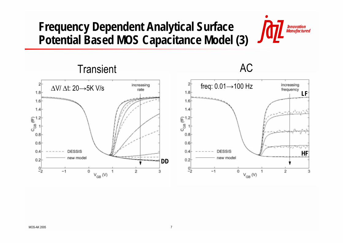
Frequency Dependent Analytical Surface Potential Based MOS Capacitance Model (1)• Inversion charge in MOS capacitor thermally generated, not supplied
by source/drain regions as in MOSFET
• Full solution requires inclusion of continuity equations, not practical for circuit simulation
• Inversion charge relaxation time approximation provides reasonable physical model suitable for circuit simulation
• Analytical surface potential solutions incorporated based on work for SP (Penn State) MOSFET model.
• Important for VCO design where DC biasing in inversion, allowinginversion charge to form, will change the frequency response
– Different than DC biasing in depletion with RF signal swinging into inversion region, inversion charge has no time to form.
• Developed and verified with device simulation in DESSIS

6
InnovationManufactured
MOS-AK 2005
Frequency Dependent Analytical Surface Potential Based MOS Capacitance Model (2)
t
tiFBGB
iii
tu
uutqtVtV
qqdtdq
Φ=
−+−Φ=−−−
−=
)()]exp(1[)]()()([ 22
)0(
ψγψ
τInversion charge (normalized) relaxation equation, qi
(0): static inversion charge generated from static analytical surface potential
Time dependent surface potential equation
normalized surface potential
∆V/ ∆t: 20→5K V/s
7
InnovationManufactured
MOS-AK 2005
Frequency Dependent Analytical Surface Potential Based MOS Capacitance Model (3)
∆V/ ∆t: 20→5K V/s freq: 0.01→100 Hz
Transient AC
LF
HFDD

8
InnovationManufactured
MOS-AK 2005
QM and PD effects
• All QM and PD effects included in model• poly inversion included for completeness, unlikely in practice

9
InnovationManufactured
MOS-AK 2005
MOS Varactor Model and X-section• Rnwb+Rnwe : Nwell resistance dominates• Rnw voltage dependence negligible
– 0.18µm and below due to heavy doping– Accumulation resistance model included in
references• Rgp: gate poly resistance (horizontal
salicided and vertical sal-poly contact)• Rgm, Rsm: interconnect resistance
including metal and vias, calculated from sheet ρρρρ, geometry and finger configuration
• Lgm, Lsm: interconnect inductance calculated from Greenhouse, geometry and finger configuration
• Dnw: well-substrate diodes• Rsub, Csub: substrate network to match
y22, usually not important since Nwell is tuning node
• CGBi: MOS cap intrinsic tuning element• Cfr: fringing and overlap capacitance,
degrades tuning for short Lg

10
InnovationManufactured
MOS-AK 2005
N+ vs. P+ Poly
VGB=0
P+ POLYN+ POLY
+_
~1Eg
• N+ poly on Nwell by self-alignment allows for shortest Lg
– highest Q– typical VCO biasing requires DC shift of tank
voltage to allow for full tuning
• P+ poly on Nwell provides entire tuning range on +VGB axis
– N+ contact to Nwell pulled back to prevent counter doping of poly
– Lg > Lmin to allow to avoid design rule violations in implanting poly with P+
– decreases Q

11
InnovationManufactured
MOS-AK 2005
MOS Varactor Layout and Metal Connection Considerations
• Metal R and L ~ NS/NF (segments)• High metal resistance (thin M1)• Low metal capacitance (M1-M1)
Metal 1
NWELL
NFGATE
NS
Metal 2
GATE
NWEL
LNS
NF
• Metal R and L ~ NF/NS (fingers)• Low metal resistance (wide M2)• High metal capacitance (M2-M1)
VS.

12
InnovationManufactured
MOS-AK 2005
Parameter Extraction: Scalable MOS Capacitance(All extraction and verification performed on 0.18µµµµm technology)
• Regression fitting of Cmax and Cmin on Wg and Lg yields DL, DW, Cfrw• Tox, Nb (well doping), QM, and PD parameters extracted from large plate capacitor
( ) ( ) ( )( ) ( )fsWgfrwWgLgoxmax NNDWCDWDLCC ⋅⋅−⋅+−⋅−⋅= 2
( ) ( ) ( ) ( )fsWgfrwWgLgdepox
depoxmin NNDWCDWDL
CCCC
C ⋅⋅
−⋅+−⋅−⋅
+
⋅= 2

13
InnovationManufactured
MOS-AK 2005
Scalable NWELL Resistance Model Extraction (1)
( )gpsmgmVmeasnwx RRRRRGB
++−= =0@
12⋅⋅
+=Wg
LgWgRR nwend
nwellρ
Lg=0 intercept yields Rend
Slope yields ρnw
• Nwell resistance dominates• Rgp, Rgm, and Rsm calculated from physical equations and subtracted from measured resistance

14
InnovationManufactured
MOS-AK 2005
Scalable NWELL Resistance Model Extraction (2)
• Plot of measured and extracted Rnwx vs. 1/Wg verifies extraction procedure

15
InnovationManufactured
MOS-AK 2005
MOS Varactor Model Verification (C&Q): Varying Lg
(@ 3G
Hz)

16
InnovationManufactured
MOS-AK 2005
MOS Varactor Model Verification (C&Q): Varying Wg
(@ 3G
Hz)
17
InnovationManufactured
MOS-AK 2005
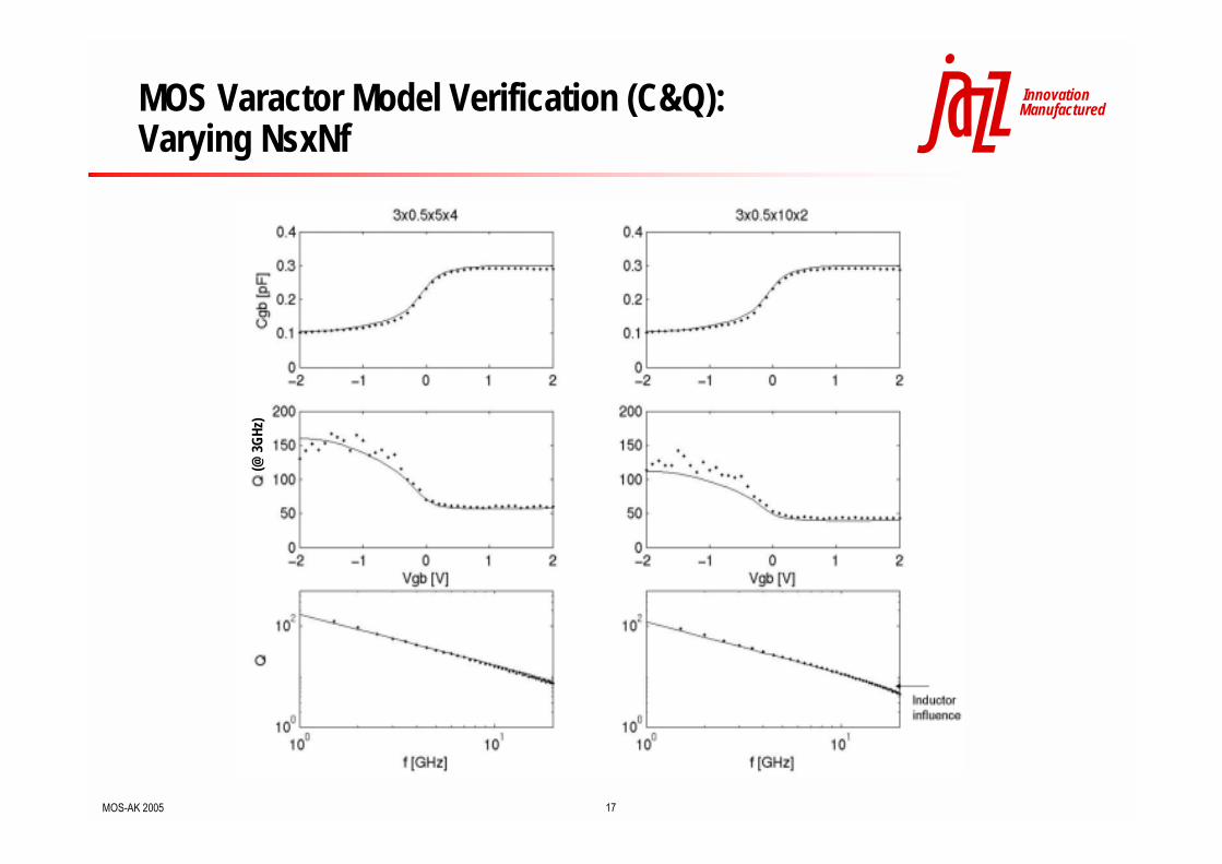
MOS Varactor Model Verification (C&Q): Varying NsxNf
(@ 3G
Hz)

18
InnovationManufactured
MOS-AK 2005
Conclusions
• First time Frequency Dependent Analytical Surface Potential Based MOS Capacitance Model, protects design from improper biasing.
• Physical scalable models for device parasitics to ensure accurate CV and Quality Factor (Q) simulation
– Scalable model provides designer option to trade CV tuning vs. Q– Physical parameter set and model provide foundation for accurate
statistical modeling of process variation• References for this material:
J. Victory, C. C. McAndrew, and K. Gullapalli, “A Time-Dependent, Surface Potential Based Compact Model for MOS Capacitors”, IEEE Electron Device Lett., vol. 22, no. 5, pp. 245-247, May 2001
J. Victory, Z. Yan, G. Gildenblat, C.C. McAndrew, J. Zheng, “A Physically Based, Scalable MOS VaractorModel and Extraction Methodology for RF Applications,” IEEE Trans. Electron Devices, vol. 52, no. 7, pp. 1343-1354, July 2005