A Photonic Crystal Slab Laplace Differentiator - arXiv.org e-Print … · 2017-11-20 · Research...
11
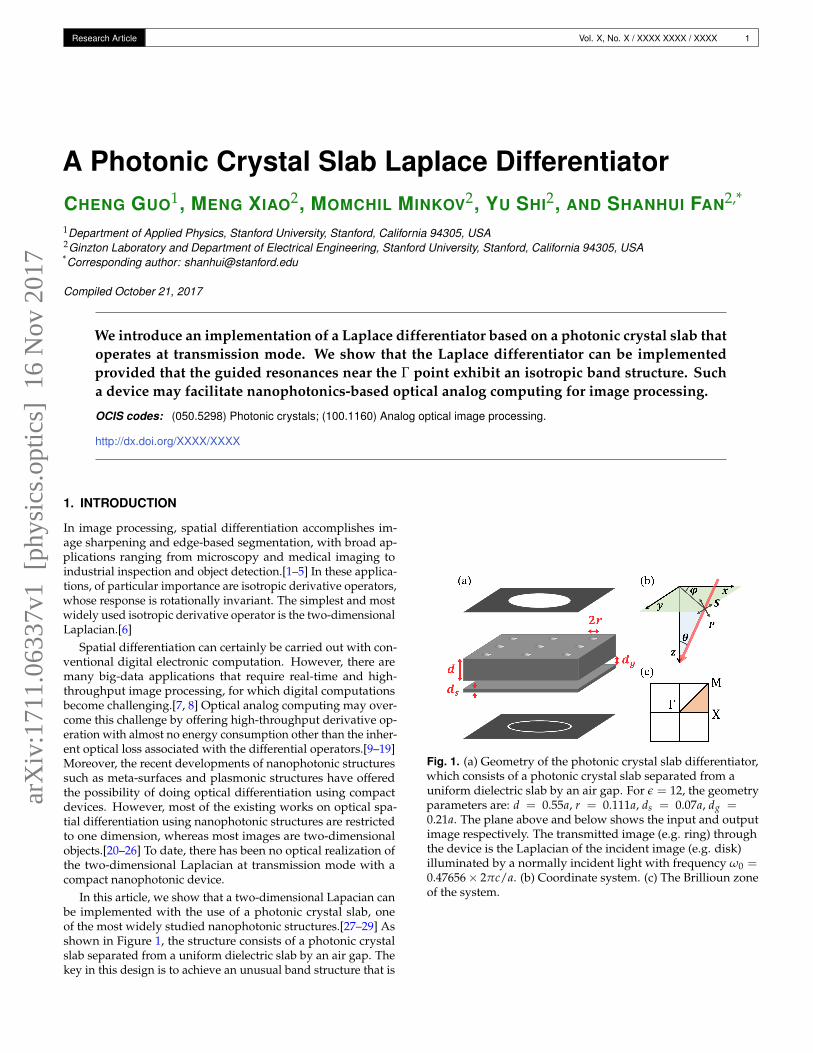
Research Article Vol. X, No. X / XXXX XXXX / XXXX 1 A Photonic Crystal Slab Laplace Differentiator CHENG GUO 1 ,MENG X IAO 2 ,MOMCHIL MINKOV 2 ,Y U S HI 2 , AND S HANHUI FAN 2,* 1 Department of Applied Physics, Stanford University, Stanford, California 94305, USA 2 Ginzton Laboratory and Department of Electrical Engineering, Stanford University, Stanford, California 94305, USA * Corresponding author: [email protected] Compiled October 21, 2017 We introduce an implementation of a Laplace differentiator based on a photonic crystal slab that operates at transmission mode. We show that the Laplace differentiator can be implemented provided that the guided resonances near the Γ point exhibit an isotropic band structure. Such a device may facilitate nanophotonics-based optical analog computing for image processing. OCIS codes: (050.5298) Photonic crystals; (100.1160) Analog optical image processing. http://dx.doi.org/XXXX/XXXX 1. INTRODUCTION In image processing, spatial differentiation accomplishes im- age sharpening and edge-based segmentation, with broad ap- plications ranging from microscopy and medical imaging to industrial inspection and object detection.[1–5] In these applica- tions, of particular importance are isotropic derivative operators, whose response is rotationally invariant. The simplest and most widely used isotropic derivative operator is the two-dimensional Laplacian.[6] Spatial differentiation can certainly be carried out with con- ventional digital electronic computation. However, there are many big-data applications that require real-time and high- throughput image processing, for which digital computations become challenging.[7, 8] Optical analog computing may over- come this challenge by offering high-throughput derivative op- eration with almost no energy consumption other than the inher- ent optical loss associated with the differential operators.[9–19] Moreover, the recent developments of nanophotonic structures such as meta-surfaces and plasmonic structures have offered the possibility of doing optical differentiation using compact devices. However, most of the existing works on optical spa- tial differentiation using nanophotonic structures are restricted to one dimension, whereas most images are two-dimensional objects.[20–26] To date, there has been no optical realization of the two-dimensional Laplacian at transmission mode with a compact nanophotonic device. In this article, we show that a two-dimensional Lapacian can be implemented with the use of a photonic crystal slab, one of the most widely studied nanophotonic structures.[27–29] As shown in Figure 1, the structure consists of a photonic crystal slab separated from a uniform dielectric slab by an air gap. The key in this design is to achieve an unusual band structure that is Fig. 1. (a) Geometry of the photonic crystal slab differentiator, which consists of a photonic crystal slab separated from a uniform dielectric slab by an air gap. For = 12, the geometry parameters are: d = 0.55a, r = 0.111a, d s = 0.07a, d g = 0.21a. The plane above and below shows the input and output image respectively. The transmitted image (e.g. ring) through the device is the Laplacian of the incident image (e.g. disk) illuminated by a normally incident light with frequency ω 0 = 0.47656 × 2πc/a. (b) Coordinate system. (c) The Brillioun zone of the system. arXiv:1711.06337v1 [physics.optics] 16 Nov 2017
Transcript of A Photonic Crystal Slab Laplace Differentiator - arXiv.org e-Print … · 2017-11-20 · Research...
Research Article Vol. X, No. X / XXXX XXXX / XXXX 1
A Photonic Crystal Slab Laplace DifferentiatorCHENG GUO1, MENG XIAO2, MOMCHIL MINKOV2, YU SHI2, AND SHANHUI FAN2,*
1Department of Applied Physics, Stanford University, Stanford, California 94305, USA2Ginzton Laboratory and Department of Electrical Engineering, Stanford University, Stanford, California 94305, USA*Corresponding author: [email protected]
Compiled October 21, 2017
We introduce an implementation of a Laplace differentiator based on a photonic crystal slab thatoperates at transmission mode. We show that the Laplace differentiator can be implementedprovided that the guided resonances near the Γ point exhibit an isotropic band structure. Sucha device may facilitate nanophotonics-based optical analog computing for image processing.
OCIS codes: (050.5298) Photonic crystals; (100.1160) Analog optical image processing.
http://dx.doi.org/XXXX/XXXX
1. INTRODUCTION
In image processing, spatial differentiation accomplishes im-age sharpening and edge-based segmentation, with broad ap-plications ranging from microscopy and medical imaging toindustrial inspection and object detection.[1–5] In these applica-tions, of particular importance are isotropic derivative operators,whose response is rotationally invariant. The simplest and mostwidely used isotropic derivative operator is the two-dimensionalLaplacian.[6]
Spatial differentiation can certainly be carried out with con-ventional digital electronic computation. However, there aremany big-data applications that require real-time and high-throughput image processing, for which digital computationsbecome challenging.[7, 8] Optical analog computing may over-come this challenge by offering high-throughput derivative op-eration with almost no energy consumption other than the inher-ent optical loss associated with the differential operators.[9–19]Moreover, the recent developments of nanophotonic structuressuch as meta-surfaces and plasmonic structures have offeredthe possibility of doing optical differentiation using compactdevices. However, most of the existing works on optical spa-tial differentiation using nanophotonic structures are restrictedto one dimension, whereas most images are two-dimensionalobjects.[20–26] To date, there has been no optical realization ofthe two-dimensional Laplacian at transmission mode with acompact nanophotonic device.
In this article, we show that a two-dimensional Lapacian canbe implemented with the use of a photonic crystal slab, oneof the most widely studied nanophotonic structures.[27–29] Asshown in Figure 1, the structure consists of a photonic crystalslab separated from a uniform dielectric slab by an air gap. Thekey in this design is to achieve an unusual band structure that is
Fig. 1. (a) Geometry of the photonic crystal slab differentiator,which consists of a photonic crystal slab separated from auniform dielectric slab by an air gap. For ε = 12, the geometryparameters are: d = 0.55a, r = 0.111a, ds = 0.07a, dg =0.21a. The plane above and below shows the input and outputimage respectively. The transmitted image (e.g. ring) throughthe device is the Laplacian of the incident image (e.g. disk)illuminated by a normally incident light with frequency ω0 =0.47656× 2πc/a. (b) Coordinate system. (c) The Brillioun zoneof the system.
arX
iv:1
711.
0633
7v1
[ph
ysic
s.op
tics]
16
Nov
201
7
Research Article Vol. X, No. X / XXXX XXXX / XXXX 2
isotropic for the two polarizations.
2. THEORETICAL ANALYSIS
Our objective is to realize a Lapacian for a two-dimensionalinput field. Specifically, for a normally incident light beam alongthe z-axis with a transverse field profile Sin(x, y), we wouldlike to design an optical device for which the transmitted beamhas a profile Sout(x, y) ∝ ∇2Sin(x, y), whre ∇2 = ∂2
x + ∂2y is the
Laplacian. The task of realizing the Laplacian ∇2 in the realspace is equivalent to designing an optical system with responsefunction
t(k) ∝ (k2x + k2
y) (1)in the wavevector space (k-space).[30] Equation (1) requires thatt(k) = 0 at |k| = 0. In a lossless photonic crystal slab, the trans-mission for normally incident light can vanish near a guidedresonance.[31] Thus we consider in more details the transmis-sion coefficient of a photonic crystal slab near normal incidence.Consider a single photonic band of guided resonances, as char-acterized by k-dependent resonant frequencies ω(k) and radia-tive linewidths γ(k). (Here k = (kx, ky) refers to the in-planewavevector.) Near the resonant frequencies, the transmittedamplitude t is expressed as [31]
t(ω, k) = td + fγ(k)
i[ω−ω(k)] + γ(k), (2)
where ω is the incident light frequency, td is the direct trans-mission coefficient, and f is related to the complex decayingamplitude of the resonance to the transmission side of the slab.
In general, f is constrained by the direct process due to energyconservation and time-reversal symmetry.[31, 32] In particular,if td = 1, that is, the direct pathway has a 100% transmissioncoefficient, then
f = −td = −1 (3)even for structure without z-mirror symmetry such as shown inFigure 1, as has been derived in Ref. [32]. In this special case,
t(ω, k) = 1− γ(k)i[ω−ω(k)] + γ(k)
. (4)
We denote ω0 = ω(k = 0), γ0 = γ(k = 0). Using Equation (4),zero transmission occurs at the Γ point when the incident wavehas the frequency:
ω = ω0 . (5)At ω = ω0, we perform an expansion of the transmission coeffi-cient t near k = 0 :
t(ω0, k) = 0 +∂t
∂ω(k)
∣∣∣Γ
δω(k) +∂t
∂γ(k)
∣∣∣Γ
δγ(k) , (6)
where
δω(k) = ω(k)−ω0, δγ(k) = γ(k)− γ0 , (7)
∂t∂ω(k)
∣∣∣Γ= − i
γ0,
∂t∂γ(k)
∣∣∣Γ= 0 , (8)
therefore,
t(ω0, k) = − iγ0
δω(k) . (9)
In this special case, t(k) is simply proportional to the banddispersion δω(k) near k = 0. If δω(k) ∝ |k|2, then t(k) ∝ |k|2as well. Therefore the transmission through a photonic crystalslab can be used to achieve the Laplacian.
The analysis above indicates that, to use a photonic crystalslab as a two-dimensional spatial differentiator, it is sufficientthat the slab satisfies the following three conditions:
1. td = 1.
2. Only one guided resonance band is coupled.
3. The band satisfies the dispersion (ω(k)−ω0) ∝ |k|2.
To satisfy the first condition above, we note that the directtransmission coefficient td is related to the non-resonant trans-mission pathway [31]. Hence it is possible to realize td = 1 by,e.g. changing the thickness of the slab. In the structure as shownin Figure 1, we achieve td = 1 by placing a uniform dielectricslab in the vicinity of the photon crystal slab, and by tuning thedistance between the slabs. This has the advantage that we cantune td without significantly affecting the band structure of thephotonic crystal slab.
To satisfy the second and third conditions above, one willneed to design the band structure for the photonic crystal slab.The design here is in fact quite non-trivial due to the vectorialnature of electromagnetic waves. Since the Laplacian is isotropicin k-space, it is natural to consider a photonic crystal slab struc-ture that has rotational symmetry. As an illustration, here weconsider a slab structure with a square lattice of air holes thathas C4v symmetry. For such a slab, it is known that at the Γpoint, which corresponds to |k| = 0, the only modes that cancouple to external plane wave must be two-fold degenerate, be-longing to a two-dimensional irreducible representation of theC4v group.[31, 33] Near such modes, in the vicinity of Γ point,the band structure in general can be described by the following2× 2 effective Hamiltonian: (See Supplementary Materials)
H(k) = (ω0 − iγ0 + a|k|2)I + b(k2x − k2
y)σz + ckxkyσx , (10)
where a, b, c are three complex coefficients, the σ’s are the Paulimatrices. This Hamiltonian has two eigenvalues of
ω±(k)− iγ±(k) = ω0 − iγ0 + a|k|2 ±√
b2(k2x − k2
y)2 + c2k2xk2
y .(11)
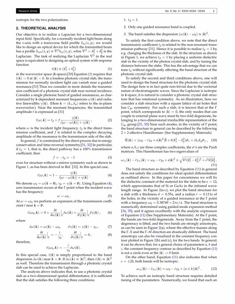
The band structure as described by Equation (11) in generaldoes not satisfy the conditions for ideal spatial differentiationas outlined above. In this paper for concreteness we will fixthe dielectric constant of the material for the slabs to be ε = 12,which approximates that of Si or GaAs in the infrared wave-length range. In Figure 2(a-c), we plot the band structure fora slab with a thickness d = 0.55a, and a radius r = 0.111a ofthe holes, in the vicinity of a guided resonance at the Γ pointwith a frequency ω0 = 0.38749× 2πc/a. The band structure isnumerically determined using guided-mode expansion method[34, 35], and it agrees excellently with the analytic expressionof Equation (11) (See Supplementary Materials). At the Γ point,the bands are two-fold degenerate. Away from the Γ point, thedegeneracy is lifted, and the two bands are strongly anisotropic,as can be seen in Figure 2(a), where the effective masses alongthe Γ-X and the Γ-M direction are drastically different. The bandanisotropy can also be visualized in the constant frequency con-tour plotted in Figure 2(b) and (c), for the two bands. In general,it can be shown that, for a general choice of parameters a, b andc, the constant frequency contour as described by Equation (11)is not a circle even at the |k| → 0 limit.
On the other hand, Equation (11) also indicates that whenc = ±2b, both bands will be isotropic:
ω±(k)− iγ±(k) = ω0 − iγ0 + (a± b)|k|2 . (12)
To achieve such an isotropic band structure requires detailedtuning of the parameters. Numerically, we found that such an
Research Article Vol. X, No. X / XXXX XXXX / XXXX 3
Fig. 2. Band structure of the photonic crystal slab with the dielectric constant ε = 12, the thickness d = 0.55a, and the radiusr = 0.111a of the holes. (a-c) Band structure near ω0 = 0.38749× 2πc/a as a typical example of conventional anisotropic bandsthat are doubly degenerate at Γ. (a) Band dispersion diagram along Γ-X and Γ-M. (b) Constant frequency contours of the lowerband with respect to (kx, ky). (c) Constant frequency contours of the upper band. (d-f) Band structure at ω0 = 0.47656× 2πc/a,which is nearly isotropic. (d) Band dispersion along Γ-X and Γ-M. (e) Constant frequency contours of the lower band. (f) Constantfrequency contours of the upper band. The frequency (ω−ω0) is in the units of 10−4 × 2πc/a, while |k|, kx and ky are in the units of10−3 × 2π/a.
isotropic band structure can be approximately achieved withthe same slab as indicated above, but near the guided resonanceat Γ with a different frequency ω0 = 0.47656× 2πc/a, wherethe complex coefficients a = 0.68− 0.14i, b = 1.11− 0.12i, c =2.24 + 0.15i, thus c/2b = 0.99 + 0.17i ≈ 1. (See SupplementaryMaterials for details.) The resulting isotropic band structuresare shown in Figure 2(d-f). In Figure 2(d), we see that the bandsalong the Γ-M and Γ-X direction have almost identical effectivemasses. And in Figure 2(e) and (f), we see that the constantfrequency contours are almost completely circular.
As we mentioned above, for a structure with C4v symmetry,the modes that a normally-incident plane wave can couple to atthe Γ point are always two-fold degenerate. Consequently, nearthe Γ point, there are always two bands of guided resonancepresent. Moreover, off the normal direction, if the direction ofincident waves is away from the high symmetry planes, bothS and P polarized lights may couple to both bands, leading tocomplex polarization conversion effects. Thus, in general, in ad-dition to having an anisotropic band structure near Γ, a photoniccrystal slab structure also does not satisfy the condition 2 aboveregarding the excitation of a single guided resonance band. Re-markably, however, below we show that once the condition foran isotropic band is satisfied, each of the two bands in fact onlycouple to one single polarization, for every direction of incidence.Below, we refer to this effect, where each polarization excitesonly a single band away from normal incidence, as the effect ofsingle-band excitation.
To illustrate the effect of single-band excitation for everydirection when the bands are isotropic, we first show that single-band excitation always occurs when the incident direction isin a mirror symmetry plane of the structure. Using the grouptheory notation in Ref. [36], as our system possesses C4v sym-metry, the doubly degenerate states at Γ are E modes. Along
the Γ-X direction, this pair of E modes splits into two singlydegenerate states of A and B modes which are even and odd,respectively, with respect to the reflection operator associatedwith the mirror plane y = 0. On the other hand, since the Sand P polarized lights are also odd and even with respect tothe same mirror plane, respectively, along the Γ-X direction, theS(P) polarized light can only couple to the B(A) modes. Thus, ingeneral, we have the effect of single-band excitation when thedirection of incidence is in a high symmetry plane such as they = 0 plane.[37]
Next, we prove the following statement: if the two-bandHamiltonian is isotropic, that is,
R(ϕ)H(k)R−1(ϕ) = H(R(ϕ)k) , (13)
for every ϕ ∈ (0, 2π), then we have the effect of single-bandexcitation along all directions. Here, R(ϕ) and R(ϕ) are therotation operators that describe the rotation around the z-axisby an angle ϕ, in the k space and the two-dimensional Hilbertspace, respectively. To prove this, we denote the eigenstatesof the two bands as |k, A〉 and |k, B〉, which connect to the Aand B modes along the Γ-X direction respectively. Equation (13)implies that:
|R(ϕ)k, A〉 = R(ϕ) |k, A〉 ,
|R(ϕ)k, B〉 = R(ϕ) |k, B〉 .(14)
We denote the S and P polarized modes as |k, S〉 and |k, P〉respectively. By definition,
|R(ϕ)k, S〉 = R(ϕ) |k, S〉 ,
|R(ϕ)k, P〉 = R(ϕ) |k, P〉 .(15)
Research Article Vol. X, No. X / XXXX XXXX / XXXX 4
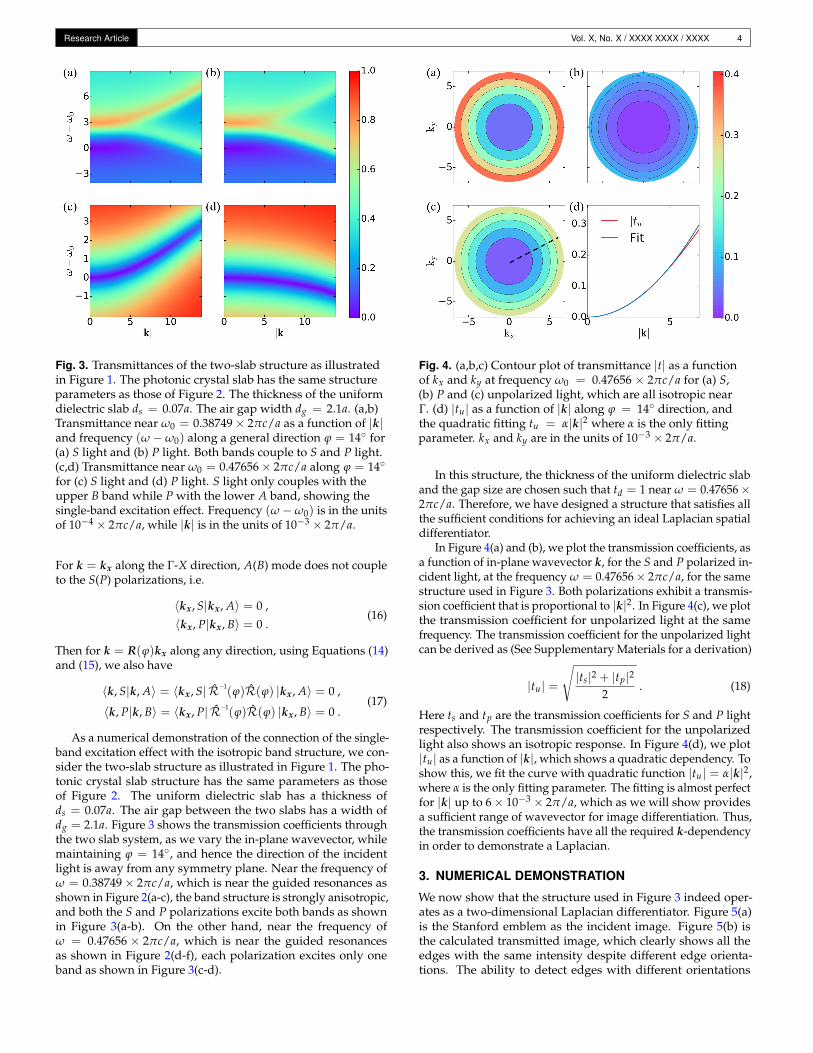
Fig. 3. Transmittances of the two-slab structure as illustratedin Figure 1. The photonic crystal slab has the same structureparameters as those of Figure 2. The thickness of the uniformdielectric slab ds = 0.07a. The air gap width dg = 2.1a. (a,b)Transmittance near ω0 = 0.38749× 2πc/a as a function of |k|and frequency (ω − ω0) along a general direction ϕ = 14◦ for(a) S light and (b) P light. Both bands couple to S and P light.(c,d) Transmittance near ω0 = 0.47656× 2πc/a along ϕ = 14◦
for (c) S light and (d) P light. S light only couples with theupper B band while P with the lower A band, showing thesingle-band excitation effect. Frequency (ω−ω0) is in the unitsof 10−4 × 2πc/a, while |k| is in the units of 10−3 × 2π/a.
For k = kx along the Γ-X direction, A(B) mode does not coupleto the S(P) polarizations, i.e.
〈kx, S|kx, A〉 = 0 ,
〈kx, P|kx, B〉 = 0 .(16)
Then for k = R(ϕ)kx along any direction, using Equations (14)and (15), we also have
〈k, S|k, A〉 = 〈kx, S| R−1(ϕ)R(ϕ) |kx, A〉 = 0 ,
〈k, P|k, B〉 = 〈kx, P| R−1(ϕ)R(ϕ) |kx, B〉 = 0 .
(17)
As a numerical demonstration of the connection of the single-band excitation effect with the isotropic band structure, we con-sider the two-slab structure as illustrated in Figure 1. The pho-tonic crystal slab structure has the same parameters as thoseof Figure 2. The uniform dielectric slab has a thickness ofds = 0.07a. The air gap between the two slabs has a width ofdg = 2.1a. Figure 3 shows the transmission coefficients throughthe two slab system, as we vary the in-plane wavevector, whilemaintaining ϕ = 14◦, and hence the direction of the incidentlight is away from any symmetry plane. Near the frequency ofω = 0.38749× 2πc/a, which is near the guided resonances asshown in Figure 2(a-c), the band structure is strongly anisotropic,and both the S and P polarizations excite both bands as shownin Figure 3(a-b). On the other hand, near the frequency ofω = 0.47656 × 2πc/a, which is near the guided resonancesas shown in Figure 2(d-f), each polarization excites only oneband as shown in Figure 3(c-d).
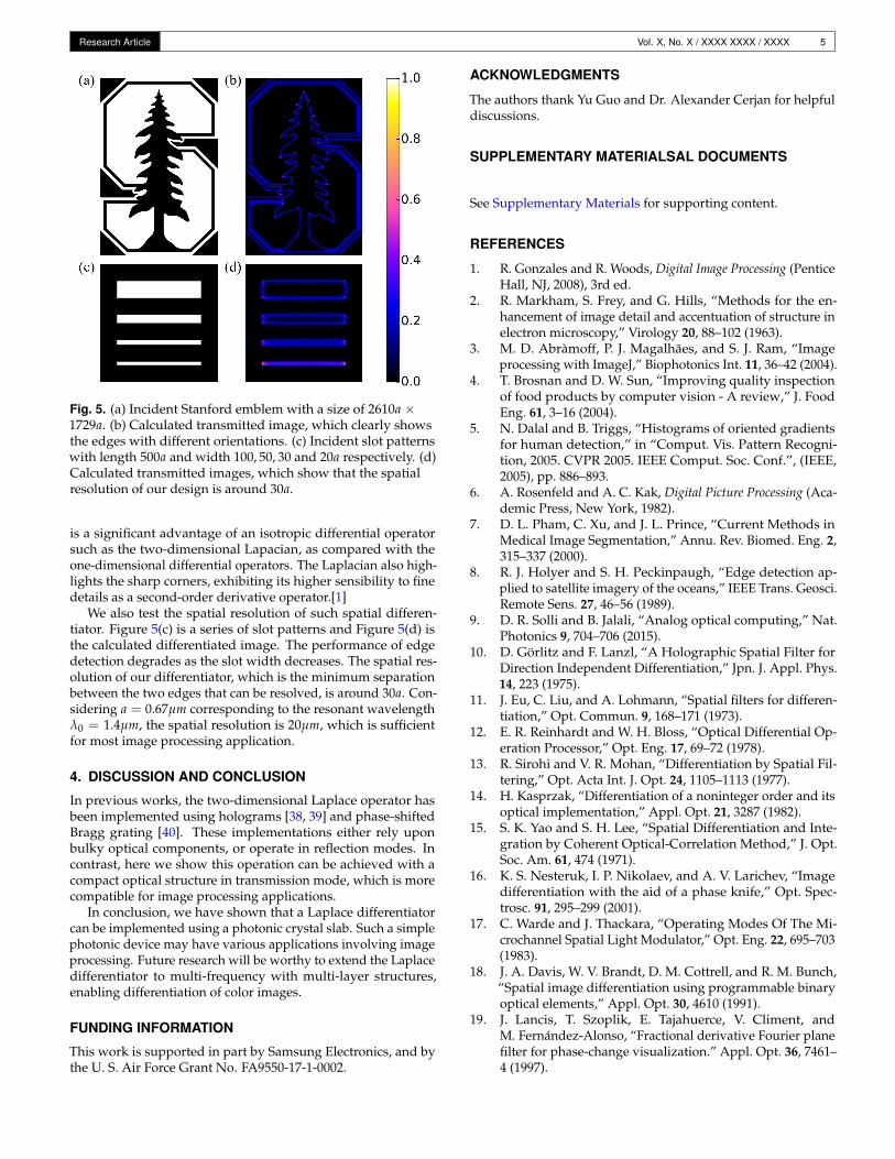
Fig. 4. (a,b,c) Contour plot of transmittance |t| as a functionof kx and ky at frequency ω0 = 0.47656 × 2πc/a for (a) S,(b) P and (c) unpolarized light, which are all isotropic nearΓ. (d) |tu| as a function of |k| along ϕ = 14◦ direction, andthe quadratic fitting tu = α|k|2 where α is the only fittingparameter. kx and ky are in the units of 10−3 × 2π/a.
In this structure, the thickness of the uniform dielectric slaband the gap size are chosen such that td = 1 near ω = 0.47656×2πc/a. Therefore, we have designed a structure that satisfies allthe sufficient conditions for achieving an ideal Laplacian spatialdifferentiator.
In Figure 4(a) and (b), we plot the transmission coefficients, asa function of in-plane wavevector k, for the S and P polarized in-cident light, at the frequency ω = 0.47656× 2πc/a, for the samestructure used in Figure 3. Both polarizations exhibit a transmis-sion coefficient that is proportional to |k|2. In Figure 4(c), we plotthe transmission coefficient for unpolarized light at the samefrequency. The transmission coefficient for the unpolarized lightcan be derived as (See Supplementary Materials for a derivation)
|tu| =√|ts|2 + |tp|2
2. (18)
Here ts and tp are the transmission coefficients for S and P lightrespectively. The transmission coefficient for the unpolarizedlight also shows an isotropic response. In Figure 4(d), we plot|tu| as a function of |k|, which shows a quadratic dependency. Toshow this, we fit the curve with quadratic function |tu| = α|k|2,where α is the only fitting parameter. The fitting is almost perfectfor |k| up to 6× 10−3 × 2π/a, which as we will show providesa sufficient range of wavevector for image differentiation. Thus,the transmission coefficients have all the required k-dependencyin order to demonstrate a Laplacian.
3. NUMERICAL DEMONSTRATION
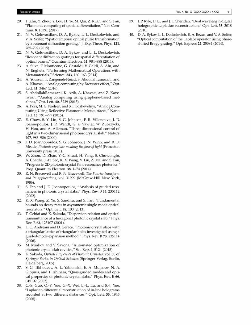
We now show that the structure used in Figure 3 indeed oper-ates as a two-dimensional Laplacian differentiator. Figure 5(a)is the Stanford emblem as the incident image. Figure 5(b) isthe calculated transmitted image, which clearly shows all theedges with the same intensity despite different edge orienta-tions. The ability to detect edges with different orientations
Research Article Vol. X, No. X / XXXX XXXX / XXXX 5
Fig. 5. (a) Incident Stanford emblem with a size of 2610a ×1729a. (b) Calculated transmitted image, which clearly showsthe edges with different orientations. (c) Incident slot patternswith length 500a and width 100, 50, 30 and 20a respectively. (d)Calculated transmitted images, which show that the spatialresolution of our design is around 30a.
is a significant advantage of an isotropic differential operatorsuch as the two-dimensional Lapacian, as compared with theone-dimensional differential operators. The Laplacian also high-lights the sharp corners, exhibiting its higher sensibility to finedetails as a second-order derivative operator.[1]
We also test the spatial resolution of such spatial differen-tiator. Figure 5(c) is a series of slot patterns and Figure 5(d) isthe calculated differentiated image. The performance of edgedetection degrades as the slot width decreases. The spatial res-olution of our differentiator, which is the minimum separationbetween the two edges that can be resolved, is around 30a. Con-sidering a = 0.67µm corresponding to the resonant wavelengthλ0 = 1.4µm, the spatial resolution is 20µm, which is sufficientfor most image processing application.
4. DISCUSSION AND CONCLUSION
In previous works, the two-dimensional Laplace operator hasbeen implemented using holograms [38, 39] and phase-shiftedBragg grating [40]. These implementations either rely uponbulky optical components, or operate in reflection modes. Incontrast, here we show this operation can be achieved with acompact optical structure in transmission mode, which is morecompatible for image processing applications.
In conclusion, we have shown that a Laplace differentiatorcan be implemented using a photonic crystal slab. Such a simplephotonic device may have various applications involving imageprocessing. Future research will be worthy to extend the Laplacedifferentiator to multi-frequency with multi-layer structures,enabling differentiation of color images.
FUNDING INFORMATION
This work is supported in part by Samsung Electronics, and bythe U. S. Air Force Grant No. FA9550-17-1-0002.
ACKNOWLEDGMENTS
The authors thank Yu Guo and Dr. Alexander Cerjan for helpfuldiscussions.
SUPPLEMENTARY MATERIALSAL DOCUMENTS
See Supplementary Materials for supporting content.
REFERENCES
1. R. Gonzales and R. Woods, Digital Image Processing (PenticeHall, NJ, 2008), 3rd ed.
2. R. Markham, S. Frey, and G. Hills, “Methods for the en-hancement of image detail and accentuation of structure inelectron microscopy,” Virology 20, 88–102 (1963).
3. M. D. Abràmoff, P. J. Magalhães, and S. J. Ram, “Imageprocessing with ImageJ,” Biophotonics Int. 11, 36–42 (2004).
4. T. Brosnan and D. W. Sun, “Improving quality inspectionof food products by computer vision - A review,” J. FoodEng. 61, 3–16 (2004).
5. N. Dalal and B. Triggs, “Histograms of oriented gradientsfor human detection,” in “Comput. Vis. Pattern Recogni-tion, 2005. CVPR 2005. IEEE Comput. Soc. Conf.”, (IEEE,2005), pp. 886–893.
6. A. Rosenfeld and A. C. Kak, Digital Picture Processing (Aca-demic Press, New York, 1982).
7. D. L. Pham, C. Xu, and J. L. Prince, “Current Methods inMedical Image Segmentation,” Annu. Rev. Biomed. Eng. 2,315–337 (2000).
8. R. J. Holyer and S. H. Peckinpaugh, “Edge detection ap-plied to satellite imagery of the oceans,” IEEE Trans. Geosci.Remote Sens. 27, 46–56 (1989).
9. D. R. Solli and B. Jalali, “Analog optical computing,” Nat.Photonics 9, 704–706 (2015).
10. D. Görlitz and F. Lanzl, “A Holographic Spatial Filter forDirection Independent Differentiation,” Jpn. J. Appl. Phys.14, 223 (1975).
11. J. Eu, C. Liu, and A. Lohmann, “Spatial filters for differen-tiation,” Opt. Commun. 9, 168–171 (1973).
12. E. R. Reinhardt and W. H. Bloss, “Optical Differential Op-eration Processor,” Opt. Eng. 17, 69–72 (1978).
13. R. Sirohi and V. R. Mohan, “Differentiation by Spatial Fil-tering,” Opt. Acta Int. J. Opt. 24, 1105–1113 (1977).
14. H. Kasprzak, “Differentiation of a noninteger order and itsoptical implementation,” Appl. Opt. 21, 3287 (1982).
15. S. K. Yao and S. H. Lee, “Spatial Differentiation and Inte-gration by Coherent Optical-Correlation Method,” J. Opt.Soc. Am. 61, 474 (1971).
16. K. S. Nesteruk, I. P. Nikolaev, and A. V. Larichev, “Imagedifferentiation with the aid of a phase knife,” Opt. Spec-trosc. 91, 295–299 (2001).
17. C. Warde and J. Thackara, “Operating Modes Of The Mi-crochannel Spatial Light Modulator,” Opt. Eng. 22, 695–703(1983).
18. J. A. Davis, W. V. Brandt, D. M. Cottrell, and R. M. Bunch,“Spatial image differentiation using programmable binaryoptical elements,” Appl. Opt. 30, 4610 (1991).
19. J. Lancis, T. Szoplik, E. Tajahuerce, V. Climent, andM. Fernández-Alonso, “Fractional derivative Fourier planefilter for phase-change visualization.” Appl. Opt. 36, 7461–4 (1997).
Research Article Vol. X, No. X / XXXX XXXX / XXXX 6
20. T. Zhu, Y. Zhou, Y. Lou, H. Ye, M. Qiu, Z. Ruan, and S. Fan,“Plasmonic computing of spatial differentiation,” Nat. Com-mun. 8, 15391 (2017).
21. N. V. Golovastikov, D. A. Bykov, L. L. Doskolovich, andV. A. Soifer, “Spatiotemporal optical pulse transformationby a resonant diffraction grating,” J. Exp. Theor. Phys. 121,785–792 (2015).
22. N. V. Golovastikov, D. A. Bykov, and L. L. Doskolovich,“Resonant diffraction gratings for spatial differentiation ofoptical beams,” Quantum Electron. 44, 984–988 (2014).
23. A. Silva, F. Monticone, G. Castaldi, V. Galdi, A. Alu, andN. Engheta, “Performing Mathematical Operations withMetamaterials,” Science. 343, 160–163 (2014).
24. A. Youssefi, F. Zangeneh-Nejad, S. Abdollahramezani, andA. Khavasi, “Analog computing by Brewster effect,” Opt.Lett. 41, 3467 (2016).
25. S. AbdollahRamezani, K. Arik, A. Khavasi, and Z. Kave-hvash, “Analog computing using graphene-based met-alines,” Opt. Lett. 40, 5239 (2015).
26. A. Pors, M. G. Nielsen, and S. I. Bozhevolnyi, “Analog Com-puting Using Reflective Plasmonic Metasurfaces,” NanoLett. 15, 791–797 (2015).
27. E. Chow, S. Y. Lin, S. G. Johnson, P. R. Villeneuve, J. D.Joannopoulos, J. R. Wendt, G. a. Vawter, W. Zubrzycki,H. Hou, and A. Alleman, “Three-dimensional control oflight in a two-dimensional photonic crystal slab.” Nature407, 983–986 (2000).
28. J. D. Joannopoulos, S. G. Johnson, J. N. Winn, and R. D.Meade, Photonic crystals: molding the flow of light (Princetonuniversity press, 2011).
29. W. Zhou, D. Zhao, Y.-C. Shuai, H. Yang, S. Chuwongin,A. Chadha, J.-H. Seo, K. X. Wang, V. Liu, Z. Ma, and S. Fan,“Progress in 2D photonic crystal Fano resonance photonics,”Prog. Quantum Electron. 38, 1–74 (2014).
30. R. N. Bracewell and R. N. Bracewell, The Fourier transformand its applications, vol. 31999 (McGraw-Hill New York,1986).
31. S. Fan and J. D. Joannopoulos, “Analysis of guided reso-nances in photonic crystal slabs,” Phys. Rev. B 65, 235112(2002).
32. K. X. Wang, Z. Yu, S. Sandhu, and S. Fan, “Fundamentalbounds on decay rates in asymmetric single-mode opticalresonators,” Opt. Lett. 38, 100 (2013).
33. T. Ochiai and K. Sakoda, “Dispersion relation and opticaltransmittance of a hexagonal photonic crystal slab,” Phys.Rev. B 63, 125107 (2001).
34. L. C. Andreani and D. Gerace, “Photonic-crystal slabs witha triangular lattice of triangular holes investigated using aguided-mode expansion method,” Phys. Rev. B 73, 235114(2006).
35. M. Minkov and V. Savona, “Automated optimization ofphotonic crystal slab cavities,” Sci. Rep. 4, 5124 (2015).
36. K. Sakoda, Optical Properties of Photonic Crystals, vol. 80 ofSpringer Series in Optical Sciences (Springer-Verlag, Berlin,Heidelberg, 2005).
37. S. G. Tikhodeev, A. L. Yablonskii, E. A. Muljarov, N. A.Gippius, and T. Ishihara, “Quasiguided modes and opti-cal properties of photonic crystal slabs,” Phys. Rev. B 66,045102 (2002).
38. C.-S. Guo, Q.-Y. Yue, G.-X. Wei, L.-L. Lu, and S.-J. Yue,“Laplacian differential reconstruction of in-line hologramsrecorded at two different distances,” Opt. Lett. 33, 1945(2008).
39. J. P. Ryle, D. Li, and J. T. Sheridan, “Dual wavelength digitalholographic Laplacian reconstruction,” Opt. Lett. 35, 3018(2010).
40. D. A. Bykov, L. L. Doskolovich, E. A. Bezus, and V. A. Soifer,“Optical computation of the Laplace operator using phase-shifted Bragg grating,” Opt. Express 22, 25084 (2014).
Supplementary Material 1
A Photonic Crystal Slab Laplace Differentiator:supplementary materialCHENG GUO1, MENG XIAO2, MOMCHIL MINKOV2, YU SHI2, AND SHANHUI FAN2,*
1Department of Applied Physics, Stanford University, Stanford, California 94305, USA2Ginzton Laboratory and Department of Electrical Engineering, Stanford University, Stanford, California 94305, USA*Corresponding author: [email protected]
Compiled October 21, 2017
This document provides supplementary information to “A Photonic Crystal Slab Laplace Dif-ferentiator”. This supplementary document consists of four sections. In Section 1, we derive theeffective Hamiltonian near the Γ point, when the states are two-fold degenerate at the Γ point.In Section 2 we provide numerical validation of the effective Hamiltonian. In Section 3, wecalculate the transmission for an arbitrary polarized state from the transmission response for Sand P polarized light. In Section 4, we plot the transmittance |t| in a larger wavevector regionfor the device configuration that operates as a differentiator. Such information on transmittanceis used in demonstrating the performance of the differentiator.
http://dx.doi.org/XXXX/XXXX
1. DERIVATION OF THE EFFECTIVE HAMILTONIAN
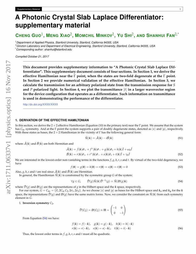
In this section, we derive the 2× 2 effective Hamiltonian (Equation (10) in the primary text) near the Γ point. We assume that the systemhas C4v symmetry. And at the Γ point the system supports a pair of doubly degenerate states, denoted as |x〉 and |y〉, respectively.With these states as bases, the 2× 2 Hamiltonian in the vicinity of Γ has the following general form:
H(k) = A(k)− iB(k) (S1)
where A(k) and B(k) are both Hermitian and
A(k) = f (k)σ+ + f ∗(k)σ− + g(k)σz + h(k) I + ω0 I
B(k) = r(k)σ+ + r∗(k)σ− + s(k)σz + t(k) I + γ0 I (S2)
We are interested in the lowest-order non-vanishing terms in the functions f , g, h, r, s and t. By virtual of the two-fold degeneracy, wehave
f (0) = g(0) = h(0) = r(0) = s(0) = t(0) = 0 (S3)
Also, g, h, s and t are real since A(k) and B(k) are Hermitian.In general, the Hamiltonian H(k) is constrained by the symmetric group G of the system:
∀g ∈ G, D(g)H(k)D−1(g) = H(D(g)k) (S4)
where D(g) and D(g) are the representations of g in the Hilbert space and the k space, respectively.For our system, G = C4v = {E, 2C4, C2, 2σv, 2σd}. As we choose |x〉 and |y〉 as bases for the Hilbert space and kx and ky for the k
space, the representations D(g) and D(g) have the same matrix forms. Now, we consider the constraint on H(k) from each symmetryelement in G.
1. Inversion symmetry C2.
D(C2) = D(C2) ≡ Π =
−1 0
0 −1
(S5)
From Equation (S4) we have:
f (k) = f (−k), g(k) = g(−k), h(k) = h(−k)
r(k) = r(−k), s(k) = s(−k), t(k) = t(−k) (S6)
Thus, the lowest order terms in f , g, h, r, s and t must all be quadratic.
arX
iv:1
711.
0633
7v1
[ph
ysic
s.op
tics]
16
Nov
201
7
Supplementary Material 2
2. Four-fold rotational symmetry C4.
D(C4) = D(C4) ≡ R =
0 1
−1 0
(S7)
From Equation (S4) we have:
f ∗(k) = − f (Rk), g(k) = −g(Rk), h(k) = h(Rk)
r∗(k) = −r(Rk), s(k) = −s(Rk), t(k) = t(Rk) (S8)
3. Mirror symmetry σv.
D(σv) = D(σv) ≡ My =
1 0
0 −1
(S9)
Here we consider the mirror plane perpendicular to the y-axis. From Equation (S4) we have:
f (k) = − f (Myk), g(k) = g(Myk), h(k) = h(Myk)
r(k) = −r(Myk), s(k) = s(Myk), t(k) = t(Myk) (S10)
The other mirror symmetry σd doesn’t provide new constraints as it can be realized with a combination of σv and C4v.Combining all the symmetry requirements, we determine the forms of the lowest order terms in all the functions. As an example,
we consider the function f (k), which can be expanded as
f (k) = Cxk2x + Cyk2
y + Cxykxky (S11)
where all the C coefficients are in general complex. Since f (k) = − f ∗(Rk) = − f (Myk), we have Cx = Cy = 0, Cxy = C∗xy ≡ C. Thusf (k) = Ckxky, where C is real. Repeating the procedures for all the functions, we summarize the results below:
f (k) = Ckxky, r(k) = C′kxky
g(k) = B(k2x − k2
y), s(k) = B′(k2x − k2
y)
h(k) = A(k2x + k2
y), t(k) = A′(k2x + k2
y) (S12)
where all the coefficients are real.Therefore, we obtain the Hamiltonian in Equation (10) of the main text.:
H(k) = (ω0 − iγ0 + a|k|2)I + b(k2x − k2
y)σz + ckxkyσx (S13)
where a = A− iA′, b = B− iB′, c = C− iC′ are the complex coefficients.
2. VALIDATION OF THE EFFECTIVE HAMILTONIAN
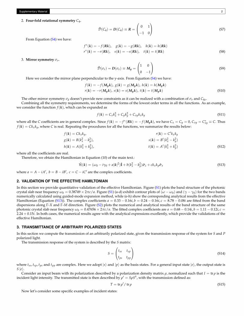
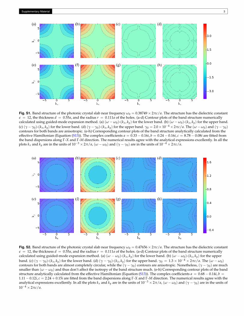
In this section we provide quantitative validation of the effective Hamiltonian. Figure (S1) plots the band structure of the photoniccrystal slab near frequency ω0 = 0.38749× 2πc/a. Figure (S1) (a-d) exhibit contour plots of (ω−ω0) and (γ− γ0) for the two bandsnumerically calculated using guided-mode expansion method, while (e-h) show the corresponding analytical results from the effectiveHamiltonian (Equation (S13)). The complex coefficients a = 0.33− 0.16i, b = 0.24− 0.16i, c = 8.78− 0.08i are fitted from the banddispersions along Γ-X and Γ-M direction. Figure (S2) plots the numerical and analytical results of the band structure of the samephotonic crystal slab near frequency ω0 = 0.47656× 2πc/a. The fitted complex coefficients are a = 0.68− 0.14i, b = 1.11− 0.12i, c =2.24 + 0.15i. In both cases, the numerical results agree with the analytical expressions excellently, which provide the validations of theeffective Hamiltonian.
3. TRANSMITTANCE OF ARBITRARY POLARIZED STATES
In this section we compute the transmission of an arbitrarily polarized state, given the transmission response of the system for S and Ppolarized light.
The transmission response of the system is described by the S matrix:
S =
tss tsp
tps tpp
(S14)
where tss, tsp, tps and tpp are complex. Here we adopt |s〉 and |p〉 as the basis states. For a general input state |e〉, the output state isS |e〉.
Consider an input beam with its polarization described by a polarization density matrix ρ, normalized such that I = tr ρ is theincident light intensity. The transmitted state is then described by ρ′ = SρS†, with the transmission defined as:
T = tr ρ′/ tr ρ (S15)
Now let’s consider some specific examples of incident states:
Supplementary Material 3
Fig. S1. Band structure of the photonic crystal slab near frequency ω0 = 0.38749× 2πc/a. The structure has the dielectric constantε = 12, the thickness d = 0.55a, and the radius r = 0.111a of the holes. (a-d) Contour plots of the band structure numericallycalculated using guided-mode expansion method. (a) (ω−ω0)-(kx, ky) for the lower band. (b) (ω−ω0)-(kx, ky) for the upper band.(c) (γ− γ0)-(kx, ky) for the lower band. (d) (γ− γ0)-(kx, ky) for the upper band. γ0 = 2.0× 10−4× 2πc/a. The (ω−ω0) and (γ− γ0)contours for both bands are anisotropic. (e-h) Corresponding contour plots of the band structure analytically calculated from theeffective Hamiltonian (Equation (S13)). The complex coefficients a = 0.33− 0.16i, b = 0.24− 0.16i, c = 8.78− 0.08i are fitted fromthe band dispersions along Γ-X and Γ-M direction. The numerical results agree with the analytical expressions excellently. In all theplots kx and ky are in the units of 10−3 × 2π/a, (ω−ω0) and (γ− γ0) are in the units of 10−4 × 2πc/a.
Fig. S2. Band structure of the photonic crystal slab near frequency ω0 = 0.47656× 2πc/a. The structure has the dielectric constantε = 12, the thickness d = 0.55a, and the radius r = 0.111a of the holes. (a-d) Contour plots of the band structure numericallycalculated using guided-mode expansion method. (a) (ω − ω0)-(kx, ky) for the lower band. (b) (ω − ω0)-(kx, ky) for the upperband. (c) (γ − γ0)-(kx, ky) for the lower band. (d) (γ − γ0)-(kx, ky) for the upper band. γ0 = 1.3× 10−4 × 2πc/a. The (ω − ω0)contours for both bands are almost completely circular, while the (γ− γ0) contours are anisotropic. Nonetheless, (γ− γ0) are muchsmaller than (ω−ω0) and thus don’t affect the isotropy of the band structure much. (e-h) Corresponding contour plots of the bandstructure analytically calculated from the effective Hamiltonian (Equation (S13)). The complex coefficients a = 0.68− 0.14i, b =1.11− 0.12i, c = 2.24 + 0.15i are fitted from the band dispersions along Γ-X and Γ-M direction. The numerical results agree with theanalytical expressions excellently. In all the plots kx and ky are in the units of 10−3 × 2π/a, (ω−ω0) and (γ− γ0) are in the units of10−4 × 2πc/a.
Supplementary Material 4
1. S polarized light
ρ = I
1 0
0 0
ρ′ = I
|tss|2 tsst∗ps
t∗sstps |tps|2
T ≡ |ts|2 = |tss|2 + |tps|2 (S16)
Similarly, for P polarized light,|tp|2 = |tsp|2 + |tpp|2 (S17)
2. Unpolarized light
ρ =I2
1 0
0 1
ρ′ =I2
|tss|2 + |tsp|2 tsst∗ps + tspt∗pp
t∗sstps + t∗sptpp |tps|2 + |tpp|2
T ≡ |tu|2 =12(|tss|2 + |tps|2 + |tps|2 + |tpp|2) (S18)
From Equation (S16-S18) we have:
|tu| =√|ts|2 + |tp|2
2(S19)
which is Equation (18) in the main text.
3. Left Circularly polarized light
ρ =I2
1 −i
i 1
ρ′ =I2
|tss|2 + |tsp|2 + i(tspt∗ss − t∗sptss) tsst∗ps + tspt∗pp + i(tspt∗ps − tsst∗pp)
t∗sstps + t∗sptpp − i(t∗sptps − t∗sstpp) |tps|2 + |tpp|2 + i(t∗pstpp − tpst∗pp)
T ≡ |tl |2 =12[|tss|2 + |tps|2 + |tps|2 + |tpp|2 + i(tspt∗ss − t∗sptss + t∗pstpp − tpst∗pp)] (S20)
which differs from Equation (S18) only in the interference term.
Note that for our system with an isotropic band structure, S is diagonal:
S =
tss 0
0 tpp
(S21)
Then the interference term in Equation (S20) disappears and we have |tl | = |tu|. So the differentiation performance will be the sameunder illumination of unpolarized or circularly polarized light.
4. TRANSMITTANCE AT LARGER WAVEVECTORS
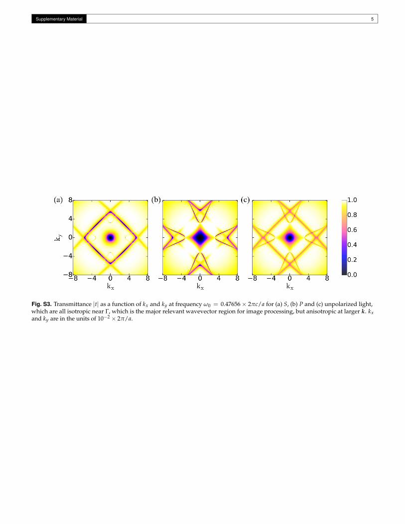
Figure (S3) plots the transmittance |t| as a function of kx and ky for S, P and unpolarized light in a larger wavevector region ascompared to Figure 4 of the primary text. All |t| are isotropic near the Γ point. They become anisotropic at larger wavevector k. Thebackground transmittances are all 1. The occurrence of transmittance dips at larger k are due to other guided resonance modes.
We calculate the performance of our differentiator based on the transmittance shown here, which covers all the relevant wavevectorregions for the incident images that we assumed.
Supplementary Material 5
Fig. S3. Transmittance |t| as a function of kx and ky at frequency ω0 = 0.47656× 2πc/a for (a) S, (b) P and (c) unpolarized light,which are all isotropic near Γ, which is the major relevant wavevector region for image processing, but anisotropic at larger k. kxand ky are in the units of 10−2 × 2π/a.