
A NOVEL SOFT-SWITCHING BUCK CONVERTER WITH COUPLED INDUCTOR · · 2014-04-27A novel topology for...
6
International Journal of Technology and Engineering System (IJTES) Vol 6. No.2 – Jan-March 2014 Pp. 113-118 ©gopalax Journals, Singapore available at : www.ijcns.com ISSN: 0976-1345 gopalax Publications 113 A NOVEL SOFT-SWITCHING BUCK CONVERTER WITH COUPLED INDUCTOR Josna Ann Joseph 1 , S.Bella Rose 2 PG Scholar, Karpaga Vinayaga College of Engineering and Technology, Chennai 1 Professor, Karpaga Vinayaga College of Engineering and Technology, Chennai 2 [email protected] 1 , [email protected] 2 ABSTRACT A novel topology for a soft-switching buck dc– dc converter with a coupled inductor is proposed. The soft- switching buck converter has advantages over the traditional hard- switching converters. The most significant advantage is that it offers a lower switching loss. This converter operates under a zero-current switching condition at turn on and a zero- voltage switching condition at turn off. It presents the circuit configuration with a least components for realizing soft switching. Because of soft switching, the proposed converter can attain a high efficiency under heavy load conditions. Likewise, a high efficiency is also attained under light load conditions, which is significantly different from other soft switching buck converters. Keywords— Buck converter, coupled inductor, soft switching, zero-current switching (ZCS), zero-voltage switching (ZVS). I. INTRODUCTION Buck converters are step-down DC-DC converters that are widely being used in different electronic devices like laptops, cell phones and also electric vehicles to obtain different level of voltages. These converters are nothing but, high frequency switching devices operating on PWM principle. The need for a lighter and smaller electronic devices propels the need for reduced size of converters operating at higher load currents. With all these inadvertent conditions the switching frequency has jumped from KHz range to MHz range. The switching devices are made to turn on and turn off the entire load current at high di/dt, and also withstand high voltage stress across them. Due to these two effects there is an increased power losses in these converters and reduces the efficiency significantly. High switching frequency can be used to drop sizes and weights of converters. Still, if converters work under hard-switching conditions, switching losses will rise as switching frequency increases, and the total efficiencies will collapse. Soft switching technologies are the best techniques to diminish switching losses, and improve efficiencies and reliabilities. Thus, the sizes of heat sinks can be reduced. The total weights and sizes of converters will also be reduced. There are many methods to gather soft switching, and the most common is using extra quasi-resonant circuits. By adding auxiliary switches, capacitors and inductors, zero-current- switching (ZCS) conditions or zero-voltage switching (ZVS) conditions can be simply achieved in quasi- resonant converters. But, high current stresses and high voltage stresses for power switches are also created. It is not favorable to select the suitable rank of power switches, because there are additional conduction losses when using higher voltage power switches. Moreover, in some converters, auxiliary switches work under hard-switching conditions. Thus, additional power losses will be produced. Due to auxiliary switches, the control technique is more complicated than that of conventional pulse width modulation converters, and extra measuring circuits of voltage and current are desired. Great amount of research is done to develop soft-switching techniques in dc–dc converters. In these converters, it is desirable to control the output voltage by pulsewidth modulation (PWM) because of its simplicity and constant frequency. The switch is turned off under ZVS condition, due to the small leakage inductance of the coupled inductors, a small voltage spike appears across the switch, and then, the switch voltage rises slowly to its final value. Thus, actually, the switch is turned off under almost ZVS condition even though the spike peak is usually much smaller than the switch maximum voltage [1]. The switching loss mechanisms include the current and voltage overlap loss during the switching interval and the capacitance loss during turn on. The diode reverse recovery also causes an additional conduction loss and further contributes to the current
Transcript of A NOVEL SOFT-SWITCHING BUCK CONVERTER WITH COUPLED INDUCTOR · · 2014-04-27A novel topology for...
International Journal of Technology and Engineering System (IJTES) Vol 6. No.2 – Jan-March 2014 Pp. 113-118
©gopalax Journals, Singapore available at : www.ijcns.com
ISSN: 0976-1345
gopalax Publications 113
A NOVEL SOFT-SWITCHING BUCK CONVERTER WITH COUPLED INDUCTOR
Josna Ann Joseph1, S.Bella Rose2
PG Scholar, Karpaga Vinayaga College of Engineering and Technology, Chennai1
Professor, Karpaga Vinayaga College of Engineering and Technology, Chennai2
[email protected], [email protected]
ABSTRACT
A novel topology for a soft-switching buck dc– dc converter with a coupled inductor is proposed. The soft-switching buck converter has advantages over the traditional hard- switching converters. The most significant advantage is that it offers a lower switching loss. This converter operates under a zero-current switching condition at turn on and a zero-voltage switching condition at turn off. It presents the circuit configuration with a least components for realizing soft switching. Because of soft switching, the proposed converter can attain a high efficiency under heavy load conditions. Likewise, a high efficiency is also attained under light load conditions, which is significantly different from other soft switching buck converters.
Keywords— Buck converter, coupled inductor, soft switching, zero-current switching (ZCS), zero-voltage switching (ZVS).
I. INTRODUCTION
Buck converters are step-down DC-DC converters that are widely being used in different electronic devices like laptops, cell phones and also electric vehicles to obtain different level of voltages. These converters are nothing but, high frequency switching devices operating on PWM principle. The need for a lighter and smaller electronic devices propels the need for reduced size of converters operating at higher load currents. With all these inadvertent conditions the switching frequency has jumped from KHz range to MHz range.
The switching devices are made to turn on
and turn off the entire load current at high di/dt, and also withstand high voltage stress across them. Due to these two effects there is an increased power losses in these converters and reduces the efficiency significantly. High switching frequency can be used to drop sizes and weights of converters. Still, if converters work under hard-switching conditions, switching losses will rise as switching frequency increases, and the total efficiencies will collapse. Soft switching technologies are the best techniques to diminish switching losses, and improve efficiencies and reliabilities. Thus, the sizes of heat sinks can be reduced. The total weights and sizes of converters will also be reduced. There are many methods to gather soft switching, and the most common is using extra quasi-resonant circuits. By adding auxiliary switches, capacitors and inductors, zero-current-
switching (ZCS) conditions or zero-voltage switching (ZVS) conditions can be simply achieved in quasi-resonant converters. But, high current stresses and high voltage stresses for power switches are also created. It is not favorable to select the suitable rank of power switches, because there are additional conduction losses when using higher voltage power switches. Moreover, in some converters, auxiliary switches work under hard-switching conditions. Thus, additional power losses will be produced. Due to auxiliary switches, the control technique is more complicated than that of conventional pulse width modulation converters, and extra measuring circuits of voltage and current are desired. Great amount of research is done to develop soft-switching techniques in dc–dc converters. In these converters, it is desirable to control the output voltage by pulsewidth modulation (PWM) because of its simplicity and constant frequency. The switch is turned off under ZVS condition, due to the small leakage inductance of the coupled inductors, a small voltage spike appears across the switch, and then, the switch voltage rises slowly to its final value. Thus, actually, the switch is turned off under almost ZVS condition even though the spike peak is usually much smaller than the switch maximum voltage [1].
The switching loss mechanisms include the
current and voltage overlap loss during the switching interval and the capacitance loss during turn on. The diode reverse recovery also causes an additional conduction loss and further contributes to the current
International Journal of Technology and Engineering System (IJTES) Vol 6. No.2 – Jan-March 2014 Pp. 113-118
©gopalax Journals, Singapore available at : www.ijcns.com
ISSN: 0976-1345
gopalax Publications 114
and voltage overlap loss. Active or passive soft-switching methods have been reported to reduce these switching losses. Recently, passive soft switching has received renewed inspection as a better alternative to active methods, because they do not require an extra switch or additional control circuitry. The two necessary components that must be added to the circuit to achieve passive zero-current turn on and zero-voltage turn off are a small inductor and capacitor. The inductor provides zero-current turn on of the active switch and limits the recovery current of the diodes while the capacitor provides zero-voltage turn off of the active switch. Traditionally, the Inductor and capacitor have been placed in series and parallel with the active switch, respectively. However, many other locations are possible and can lower the component count and reduce switch stress.[2] To create ZC condition for switch turn-on is to have a snubber inductor in series with the switch or diode. However, at turnoff, this inductor will cause a voltage spike on the switch. Therefore, a pulse current source is required to provide the output current, and, thus, the switch can be turned off under ZC condition while preventing the voltage spikes. To reduce the number of circuit elements, the pulse current source path and the required snubber inductor to decrease turn-on losses can be combined for a buck converter. A pulse voltage source can be applied to the snubber inductor and create the required pulse current source at switch turnoff.[3] The pulsewidth modulation technique is praised for its high power capability, fast transient response, and ease of control. The pulsewidth-modulated (PWM) dc–dc converters have also been widely used in industry. For minimization of size and weight, increasing switching frequency in the PWM converter is required. However, increasing switching frequency will result in more switching losses and electromagnetic interference (EMI). Recently, for solving this problem, a number of soft-switching PWM techniques are available, aimed at combining required features of both the conventional PWM and resonant techniques. The zero-voltage-switching (ZVS) methods are necessary for the majority of semiconductor devices such as MOSFETs, since the turn-on loss produced by the output capacitance is large. The zero-current-switching (ZCS) approaches are suitable for the minority of carrier semiconductor devices. [4]
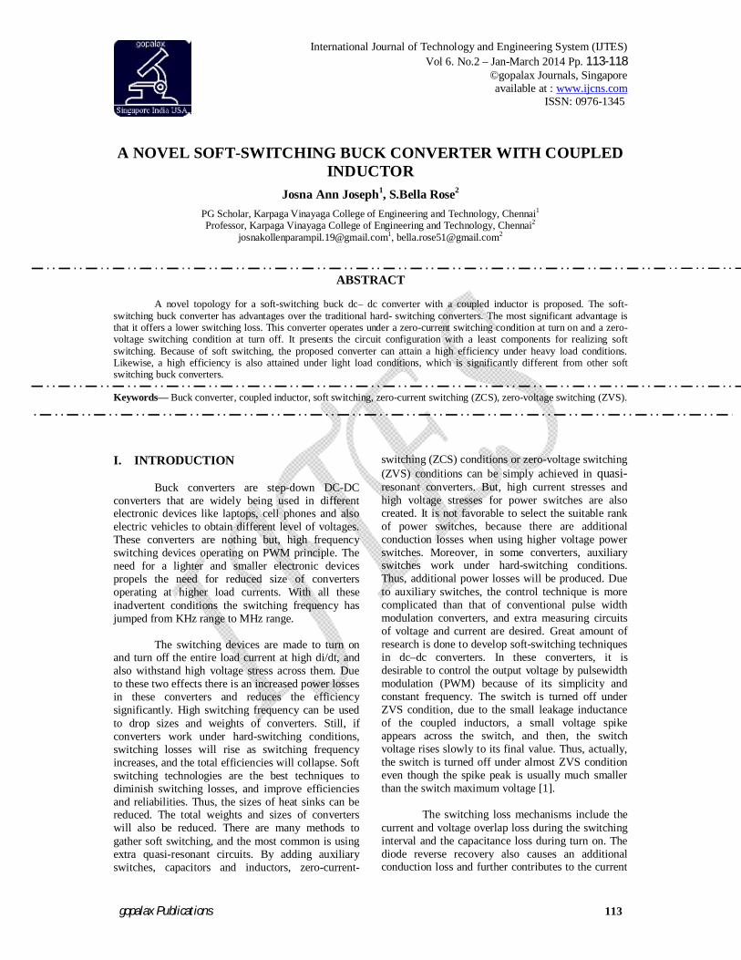
Fig. 1. Topology of the proposed ZCS–ZVS buck converter.
In most soft-switching converters, efficiencies can be improved significantly under heavy load conditions, but as in [5] effects are not good under light load conditions. It is generally because of additional power dissipations of auxiliary circuit . To solve the low-efficiency problem at a light load, based on a ZVS converter, an improved soft-switching buck converter with coupled inductor is proposed.
II. PRINCIPLE OF OPERATION
Fig. 1 shows topology of the proposed ZCS–ZVS buck converter. In this topology, inductors L1 and L2 are coupled [6][7]inductors. S1 and D1 are the main power switches, like a conventional buck converter. D2 is an extra diode. The theoretical current waveforms of L1, L2 , and L3 of the proposed converter at steady state are shown in Fig.2. The main switch S1 and the diode D1 are in off condition .The load current is freewheeling through the
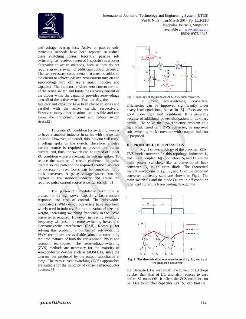
Fig. 2 . The theoretical current waveforms of L1, L2 , and L3 of
the proposed converter D2. Because L3 is very small, the current of L3 drops quicker than that of L1, and also reduces to zero before S1 turns ON. It offers the ZCS condition for S1. Due to snubber capacitor Cr1, S1 can turn OFF
International Journal of Technology and Engineering System (IJTES) Vol 6. No.2 – Jan-March 2014 Pp. 113-118
©gopalax Journals, Singapore available at : www.ijcns.com
ISSN: 0976-1345
gopalax Publications 115
under a ZVS condition. Cp1 is the parasitic capacitance of the MOSFET S1.
Associated on the waveforms of the inductor currents, one switching period is allocated into five intervals, as shown in Fig.2, Equivalent circuits for each interval are established. In Fig.2, kij shows a slope of inductor currents at a different mode, where i denotes the number of the inductor and j represents the number of the different operating mode. The detailed theoretical analyses for each mode will be given as follows.
1) Mode 1 [t0−t1]:
At t0, S1 is triggered to conduct. Due to L3, is1 will increase slowly, so S1 can turn ON under a ZCS condition. Resonance occur between L3 and Cr1.Then, i3 and i1 will increase, and i2 will go down. Since L3 is very small, the current-rising level of L3 is larger than L1. At t1, i3 and i1 are equal. It means that D2 turns OFF automatically, and this mode ends.
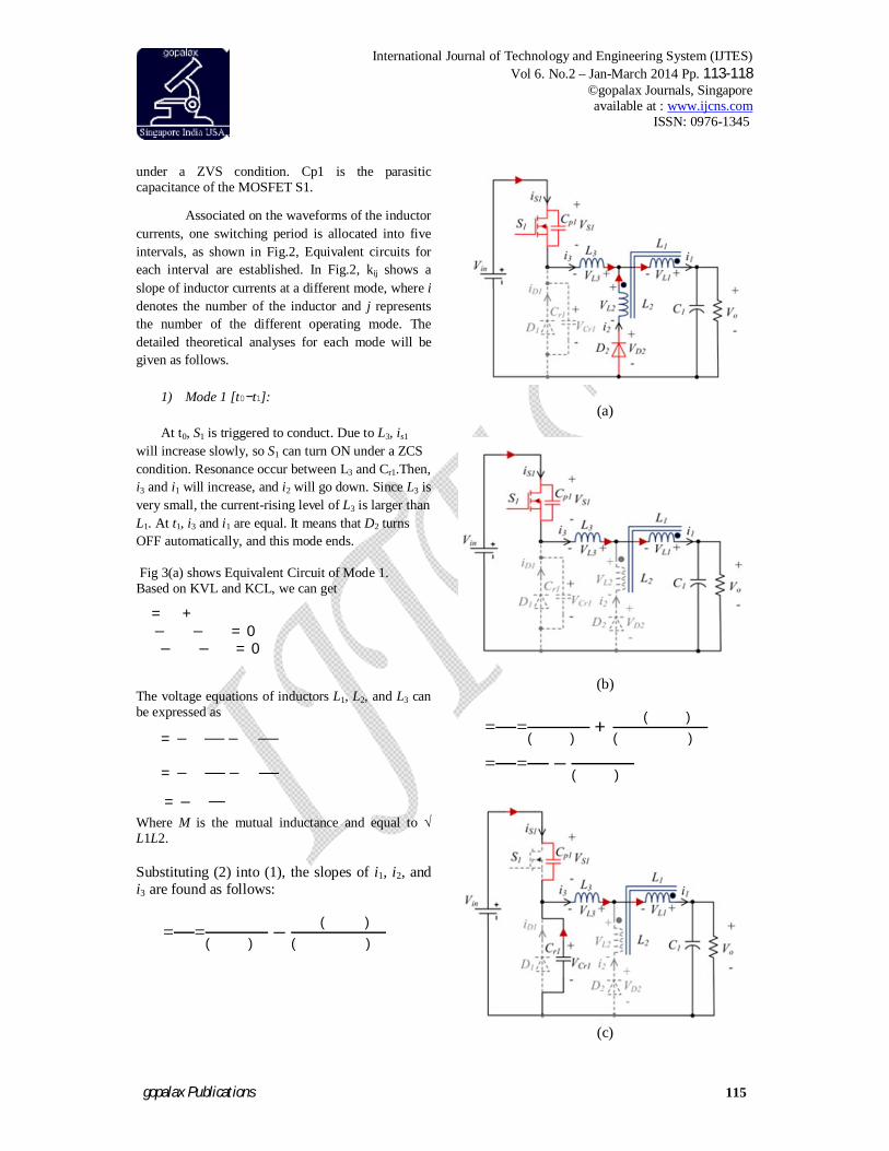
Fig 3(a) shows Equivalent Circuit of Mode 1. Based on KVL and KCL, we can get
= + − − = 0 − − = 0
The voltage equations of inductors L1, L2, and L3 can be expressed as
= − −
= − −
= − Where M is the mutual inductance and equal to √ L1L2. Substituting (2) into (1), the slopes of i1, i2, and i3 are found as follows:
= =( )
− ( )( )
(a)
(b)
= =( )
+ ( )( )
= = −( )
(c)
International Journal of Technology and Engineering System (IJTES) Vol 6. No.2 – Jan-March 2014 Pp. 113-118
©gopalax Journals, Singapore available at : www.ijcns.com
ISSN: 0976-1345
gopalax Publications 116
(d)
(e) 2) Mode 2 [t1−t2 ]
At t1, i3 and i1 are identical, and both increase linearly and i2 is zero. In this mode, D2 is always OFF, and the branch of L2 does not work. At t2, S1 turns OFF, and this mode ends. It is similar to a conventional buck converter. Fig 3(b) shows Equivalent Circuit of Mode 2. Based on KVL, we can get
= = 0 − − − = 0
Fig. 3. Equivalent circuits for each operation
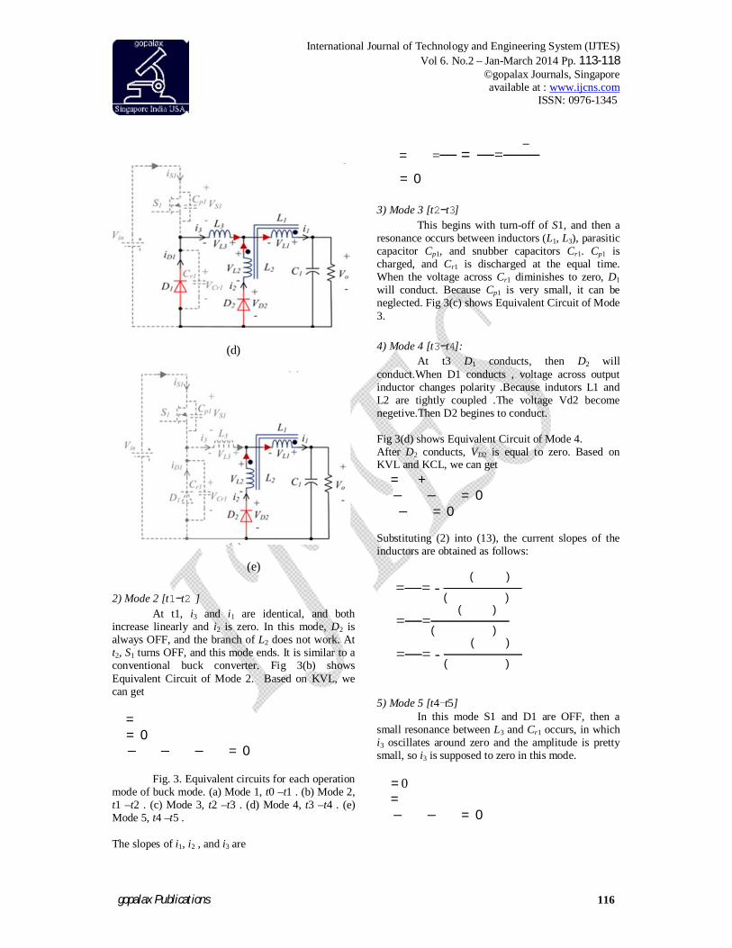
mode of buck mode. (a) Mode 1, t0 –t1 . (b) Mode 2, t1 –t2 . (c) Mode 3, t2 –t3 . (d) Mode 4, t3 –t4 . (e) Mode 5, t4 –t5 . The slopes of i1, i2 , and i3 are
= = = = –
= 0 3) Mode 3 [t2−t3]
This begins with turn-off of S1, and then a resonance occurs between inductors (L1, L3), parasitic capacitor Cp1, and snubber capacitors Cr1. Cp1 is charged, and Cr1 is discharged at the equal time. When the voltage across Cr1 diminishes to zero, D1 will conduct. Because Cp1 is very small, it can be neglected. Fig 3(c) shows Equivalent Circuit of Mode 3. 4) Mode 4 [t3−t4]: At t3 D1 conducts, then D2 will conduct.When D1 conducts , voltage across output inductor changes polarity .Because indutors L1 and L2 are tightly coupled .The voltage Vd2 become negetive.Then D2 begines to conduct. Fig 3(d) shows Equivalent Circuit of Mode 4. After D2 conducts, VD2 is equal to zero. Based on KVL and KCL, we can get
= + − − = 0 − = 0
Substituting (2) into (13), the current slopes of the inductors are obtained as follows:
= = - ( )
( )
= = ( )
( )
= = - ( )
( )
5) Mode 5 [t4−t5]
In this mode S1 and D1 are OFF, then a small resonance between L3 and Cr1 occurs, in which i3 oscillates around zero and the amplitude is pretty small, so i3 is supposed to zero in this mode.
=0 = − − = 0
International Journal of Technology and Engineering System (IJTES) Vol 6. No.2 – Jan-March 2014 Pp. 113-118
©gopalax Journals, Singapore available at : www.ijcns.com
ISSN: 0976-1345
gopalax Publications 117
As shown in Fig. 2, the current just flows through L1 and L2 , i.e., i1 is equal to i2 . Therefore, the slopes of i1, i2 , and i3 can be easily obtained as follows
= =-( )
= =-( )
=0
A common method of controlling this type
of circuit is pulse width modulation (PWM), which controls the power switch by applying a voltage signal to its gate and varying its ON and OFF times. The ratio of ON time to switching period is the duty cycle. With pulse-width modulation control, the regulation of output voltage is achieved by varying the duty cycle of the switch, keeping the frequency of operation constant. Duty cycle refers to the ratio of the period for which the power semiconductor is kept ON to the cycle period.
Idea of coupled inductor to create soft switching and L1 is the main inductor[8]-[11]. Coupled inductors are used extensively in electrical applications. Their properties allow for increasing or decreasing voltage and current, transferring impedance through a circuit, and they can isolate two circuits from each other electrically.
When the ideal switches of a dc-dc converter are implemented using current unidirectional and/or voltage-unidirectional semiconductor switches, one or more new modes of operation known as discontinuous conduction modes (DCM) can occur. The discontinuous conduction mode arises when the switching ripple in an inductor current or capacitor voltage is large to cause the polarity of the applied switch current or voltage to reverse, the current- or voltage-unidirectional assumptions made in gathering the switch with semiconductor devices are violated. The DCM is commonly witnessed in dc-dc converters and rectifiers, and can also sometimes happen in inverters or in other converters containing two-quadrant switches.
The discontinuous conduction mode typically occurs with large inductor current ripple in a converter operating at light load and containing current-unidirectional switches. Since it is usually required that converters operate with their loads removed, DCM is frequently encountered. Indeed, some converters are purposely designed to operate in DCM for all loads.
III. SIMULATION
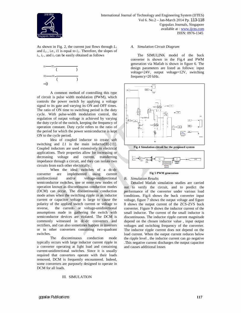
A. Simulation Circuit Diagram The SIMULINK model of the buck
converter is shown in the Fig.4 and PWM generation via Matlab is shown in figure 6. The design parameters are listed as follows: input voltage=24V, output voltage=12V, switching frequency=20 kHz.
Fig 4 Simulation circuit for the proposed system
Fig 5 PWM generation
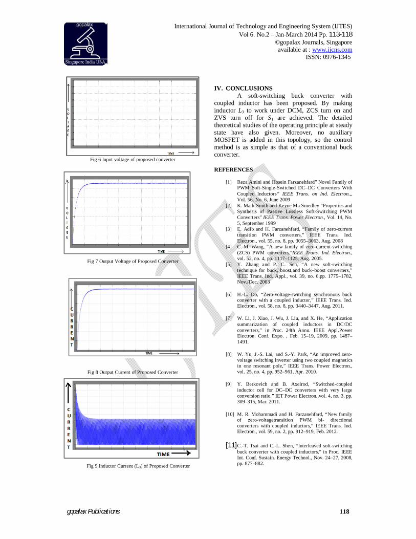
B. Simulation Results Detailed Matlab simulation studies are carried
out to verify the circuit, and to predict the performance of the converter under various load conditions. Fig.6 shows the buck converter input voltage, figure 7 shows the output voltage and figure 8 shows the output current of the ZCS-ZVS buck converter. Figure 9 shows the inductor current of the small inductor. The current of the small inductor is discontinuous. The inductor ripple current magnitude depend on the chosen inductor value , input output voltages and switching frequency of the converter. The inductor ripple current does not depend on the load current. When the output current reduces below the ripple level , the inductor current can go negative .This negative current discharges the output capacitor and causes additional losses
International Journal of Technology and Engineering System (IJTES) Vol 6. No.2 – Jan-March 2014 Pp. 113-118
©gopalax Journals, Singapore available at : www.ijcns.com
ISSN: 0976-1345
gopalax Publications 118
Fig 6 Input voltage of proposed converter
Fig 7 Output Voltage of Proposed Converter
Fig 8 Output Current of Proposed Converter
Fig 9 Inductor Current (L3) of Proposed Converter
IV. CONCLUSIONS
A soft-switching buck converter with coupled inductor has been proposed. By making inductor L3 to work under DCM, ZCS turn on and ZVS turn off for S1 are achieved. The detailed theoretical studies of the operating principle at steady state have also given. Moreover, no auxiliary MOSFET is added in this topology, so the control method is as simple as that of a conventional buck converter.
REFERENCES
[1] Reza Amini and Hosein Farzanehfard” Novel Family of
PWM Soft-Single-Switched DC–DC Converters With Coupled Inductors” IEEE Trans. on Ind. Electron.,, Vol. 56, No. 6, June 2009
[2] K. Mark Smith and Keyue Ma Smedley “Properties and Synthesis of Passive Lossless Soft-Switching PWM Converters” IEEE Trans. Power Electron., Vol. 14, No. 5, September 1999
[3] E. Adib and H. Farzanehfard, “Family of zero-current transition PWM converters,” IEEE Trans. Ind. Electron., vol. 55, no. 8, pp. 3055–3063, Aug. 2008
[4] C.-M. Wang, “A new family of zero-current-switching (ZCS) PWM converters,”IEEE Trans. Ind. Electron., vol. 52, no. 4, pp. 1117–1125, Aug. 2005.
[5] Y. Zhang and P. C. Sen, “A new soft-switching technique for buck, boost,and buck–boost converters,” IEEE Trans. Ind. Appl., vol. 39, no. 6,pp. 1775–1782, Nov./Dec. 2003
[6] H.-L. Do, “Zero-voltage-switching synchronous buck converter with a coupled inductor,” IEEE Trans. Ind. Electron., vol. 58, no. 8, pp. 3440–3447, Aug. 2011.
[7] W. Li, J. Xiao, J. Wu, J. Liu, and X. He, “Application summarization of coupled inductors in DC/DC converters,” in Proc. 24th Annu. IEEE Appl.Power Electron. Conf. Expo. , Feb. 15–19, 2009, pp. 1487–1491.
[8] W. Yu, J.-S. Lai, and S.-Y. Park, “An improved zero-voltage switching inverter using two coupled magnetics in one resonant pole,” IEEE Trans. Power Electron., vol. 25, no. 4, pp. 952–961, Apr. 2010.
[9] Y. Berkovich and B. Axelrod, “Switched-coupled inductor cell for DC–DC converters with very large conversion ratio,” IET Power Electron.,vol. 4, no. 3, pp. 309–315, Mar. 2011.
[10] M. R. Mohammadi and H. Farzanehfard, “New family of zero-voltagetransition PWM bi- directional converters with coupled inductors,” IEEE Trans. Ind. Electron., vol. 59, no. 2, pp. 912–919, Feb. 2012.
[11]C.-T. Tsai and C.-L. Shen, “Interleaved soft-switching buck converter with coupled inductors,” in Proc. IEEE Int. Conf. Sustain. Energy Technol., Nov. 24–27, 2008, pp. 877–882.


![Modeling and Control of a Multi-stage Interleaved …by Cuk in buck-boost converter [6], [7]. In [8], Witulski has shown how a coupled inductor´ differs from normal inductor and transformer.](https://static.fdocuments.in/doc/165x107/5f4d972268593756d475e471/modeling-and-control-of-a-multi-stage-interleaved-by-cuk-in-buck-boost-converter.jpg)