A NOVEL SILICON MICROMACHINED … NOVEL SILICON MICROMACHINED INTEGRATED MCM THERMAL MANAGEMENT...
49
A NOVEL SILICON MICROMACHINED INTEGRATED MCM THERMAL MANAGEMENT SYSTEM Progress report (year 2) and project renewal request for year 3 hnding NASA Lewis Research Center Brookpark, Ohio Performance period: March 1, 1998 to February 28, 1999 M. J. Kazmierczak, Department of Mech and Nuclear Engineering (513) 556-0259 Department of Electrical and Computer Engineering (5 13) 5564774 F.M. Gerner, Department of Mechanical, Industrial and Nuclear Engineering (5 13) 5562646 https://ntrs.nasa.gov/search.jsp?R=19980009290 2018-05-30T18:59:38+00:00Z
Transcript of A NOVEL SILICON MICROMACHINED … NOVEL SILICON MICROMACHINED INTEGRATED MCM THERMAL MANAGEMENT...

A NOVEL SILICON MICROMACHINED INTEGRATED MCM THERMAL MANAGEMENT SYSTEM
Progress report (year 2) and project renewal request for year 3 hnding
NASA Lewis Research Center Brookpark, Ohio
Performance period: March 1, 1998 to February 28, 1999
M. J. Kazmierczak, Department of Mech
and Nuclear Engineering (513) 556-0259
Department of Electrical and Computer Engineering
(5 13) 5564774
F.M. Gerner, Department of Mechanical, Industrial
and Nuclear Engineering (5 13) 5562646
https://ntrs.nasa.gov/search.jsp?R=19980009290 2018-05-30T18:59:38+00:00Z
TABLE OF CONTENTS
Table of Contents ' ii
List eeF;gares ....................................................................................................... iv
I. SUMMARY .................................................................................................... 1
II. PROJECT DESCRIPTION (Overall)
A. Introducdon ......................................................................................... 2
B. Original Scope of Work ...................................................................... 3
C. Additional Focus (Porous Wick) ......................................................... 4
HI. PAST YEAR IN REVIEW (Accomplishments)
A. MCM - Thermal Management System
1. Microfabrication Update
a) MCM and chip-in-board ............................................... 6
b) cooling channels ...................................................... l I
2. Thermal Analysis Update
a) microchannel cooling performance experiments ............. 12
b) simplified modeling of MCM card-to-integrated rack.. :. 15
c) thermal contactconductance theory................................18
d) thermal contact conductance experiments
i) chip-to-MCM card (3-D exp.) ............................. 20
W
B. Porous Wick Structure
1. Microfabric_otx Background and overview of technique ......... 22
2. Etchin8 system setup..................................................................23
3. Microfabrication of Porous Structures
a) preliminary samples ....................................................... 25
b) tmoe_s, with 5 micron holes with 20 micron pitch. ......... 26
4. Characterization of Porous Wick Properties
a) porosity and permeability: theoretical calculations ......... 27
b) porosity and permeability: experimental testing ............. 30
c) effective thermal conductivity ........................................ 32

IV PLA,\_ED WORK(Year 3 Goals)
A. MCM-Thermal Management System
I MCM and chip-in-MCM card
a, Microfabrication ..........................................................
i) electrical interconnects (external)
ii) electrical interconnects (internal)
iii) smart sensors
b. Thermal analysis ..........................................................
i) experimental test set-up and
contact conductance experiments
ii) 3-D finite difference modeling
iii) 1-D silicon-to-silicon contact
resistance experiments
2. MCM card-in-Integrated rack
a. Thermal analysis ..........................................................
i) 3-D finite difference modeling
ii) test section (without contact resistance)
36
38
42
m
B. Porous Wick Structure .......................................... ...................
1. Microfabrication of Porous Silicon Structures
2. Testing of Porous Silicon Samples
3. Microfabricafion of Advanced Porous StructuresI
C. Time-Table of Planned Work
44
V. CLOSING .................................................................................................... 46
VI. BIBLIOGRAPHY ........................................................................................ 47
VII. BUDGET .................................................................................................... 49
Appendix A: Conference Papers
tit

Figure i -
Figure 2 -
Figure 3 -
LIST OF FIGLRES
Micro heat pipes on a silicon wafer
Micro flow sensor device
3-D high density MCM Thermal Management System
Figure 4 - Loop heat pipe schematic
Figure 5 - Multi-Chip Module, IC carrier board (MCM-board) and integr_ed thermal
management system (single slot backside cooling channel) in (100) silicon
Figure 6 - (Photograph), partial view of wafer during chip etching from wafer backside
Figure 7 - .Silicon chips which have been batch fabricated and sepmlted by _fisotropic
KOH etching with deposited metal heater and tern_e sensors
Figure 8 - (Photograph), MCM-board fabricated in 2" silicon wafer containing two fully
integrated chips and two receiving pockets
Figure 9 - IR-spectra of SiO: grown by thermal wet oxidation and plasma deposition
Figure 10 - XPS-spectrum of plasma-deposited film with Ou'i_os flow ratio of 10 and
3 reTort total pressure
Figure 11 - Degraded microchannel cross-section caused by oxygen precipitation
Figure 12 - Improved microchannel cross-section using high t_ treatment
Figure 13 - Predicted performance of maximum chip heat flux in MCM card cooled by
integrated rack based on simple I-D heat conduction models
Figure 14 - Sketch of _nttact conductance problems encountered in MCM / Thermal
Management System
Figure 15 - Sketch of contact resistance experiments showing measured temperatures
Figure 16 - Sketch ofetch rig and control loop
Figure 17 - Photograph of the light source u,lth etch rig
Figure 18 - Photograph of the PC and HP tnstruments
Figure 19 - Randomly distributed pores showing that the theory principally-works
IV

LIST OF FIGURES (continued)
Figure 20 - Successful pore initiation using mask
Figure 21 - Etched sample showing that too high of doping concentration leads to
branching
Figure 22 - First successful sample: 5 micron holes and 20 micron pitch etched
to a depth of 170 microns
Figure 23 - The same sample after etching the remaining silicon from the backside "
Figure 24 - Deeper etching reveals some very slight pore widening
Figure 25 - Theoretical permeability of the micromachined porous wick structure as a
function of selected pore radius and pitch
Figure 26 - Porous wick test sample holder and testing loop
Figure 27 - Thermal conductivity (theoretical) of porous wick as a _mction of porosity
Figure 28 - Design of printed circuit board used for external connections"
Figure 29 - MCM-board showing electrical interconnection layer deposited by thin film
technology
Figure 30 - Schematic for thermal and electrical testing of MCM prototype
Figure 31 - Aluminum test block design to simulate thermal cooling performance of
MCM card in IR rack without contact resistance
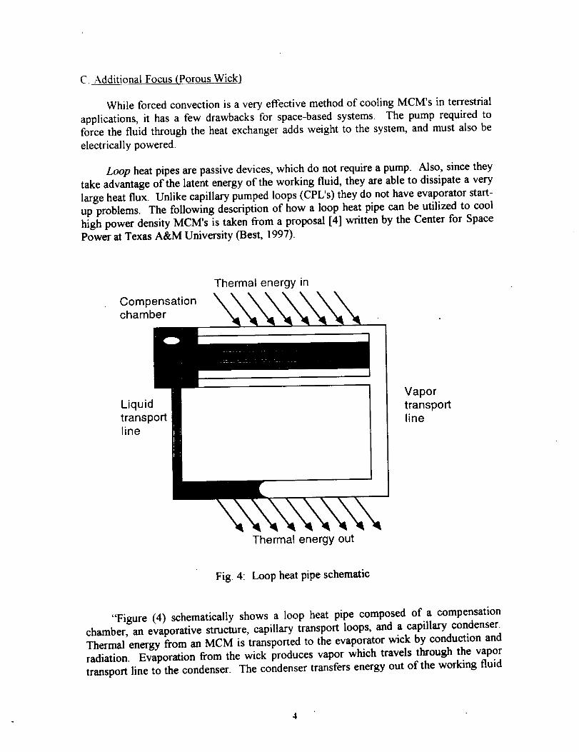
C. Additional Focus (Porous Wick)
While forced convection is a very effective method of cooling MCM's in terrestrial
applications, it has a few drawbacks for space-based systems. The pump required to
force the fluid through the heat exchanger adds weight to the system, and must also be
electrically powered.
Loop heat pipes are passive devices, which do not require a pump. Also, since they
take advantage of the latent energy of the working fluid, they are able to dissipate a very
large heat flux. Unlike capillary pumped loops (CPL's) they do not have evaporator start-
up problems. The following description of how a loop heat pipe can be utilized to cool
high power density MCM's is taken from a proposal [4] written by the Center for Space
Power at Texas A&M University (Best, 1997).
Compensationchamber
Thermal energy in
Liquid
transportline
Vapor
transportline
Thermal energy out
Fig. 4: Loop heat pipe schematic
"Figure (4) schematically shows a loop heat pipe composed of a compensation
chamber, an evaporative structure, capillary transport loops, and a capillary condenser.
Thermal energy from an MCM is transported to the evaporator wick by conduction and
radiation. Evaporation from the wick produces vapor which travels through the vapor
transport line to the condenser. The condenser transfers energy out of the working fluid
4
to a lower temperatureexternalsink, convening the vapor to single phase liquid. The
liquid returns to the evaporator through the liquid transport line which passes through the
compensation chamber. The compensation chamber acts as an inventory controller forthe system."
Currently one of the major limitations of a loop heat pipes ability to dissipate largeheat fluxes is the porous wick. Conventional sintered particle wicks have a distribution
of pore size and spacing which limit wick performance and hence maximum heat load for
the loop heat pipe. Since the radii of curvature of the miniscus depends on pore size, the
least favorable pore size determines the performance of the wick.
Several years ago it was found that under the proper conditions an HF-based
electrolytic fluid will etch a porous "sponge-like" structure in silicon, where the walls,
remain single crystalline silicon, as shown by x-ray analysis. The porosity will show an
anisotropic directionality lying along the predominant current flow direction,
perpendicular to the semiconductor surface. In recent years, several research groups have
pursued the electroluminescense properties where the surface will continue to glow after
being initially exposed to intense light. However, the controllability of the pore sizes, the
porosity (volume occupied by etched-out open space) and the thermal properties are of
interest in this work.
Also, etching activity can be lithographically patterned as with integrated circuits,
and supplemental control can be had by adjusting the molarity of the etchant, the driving
current, the local crystal doping (more activity in p+ regions) and even the intensity of
directed light (as with a laser). Also, one can grow silicon dioxide on the surfaces of the
pore walls under a high temperature oxide atmosphere (as we do in microelectronic
t_abrication), thus since oxide adds to the wall thickness we can fine-tune the pore size.
Of course the oxide thermal properties are different (lower) than that of silicon, thus we
can adjust the thermal properties after fabrication.
Micro-fabricating a porous wick in silicon allows one to create pores of uniform
size and spacing. Also, it is possible to vary the diameter of individual pores across the
thickness of the wick. This nay greatly increase the maximum heat load for a layered
heat pipe by preventing the miniscus from receding all of the way intothe liquid. The
goal of thispart of our research isto createpores with diameter of order I micron and
thereby greatly improve the thermal performance of loop heat pipes.
I1]. PAST YEAR IN REVIEW (Accomplishments)
B. Porous Wick Structure
1. Microfabrication of Porous Silicon: Background Information and Technique
In order to improve the performance of loop heat pipes it is necessary to fabricate a
wick with a pore size of approximately 1 micron. Traditionally, porous silicon etchingresults in a sponge-like structure with pore sizes distributed from nanometers to hundredsof nanometers.
On the other hand, macro porous silicon can create arrays of straight and uniform
holes through a flat silicon wafer. This type of' porous structure is expected to yield better
performance than the usual sponge-like ones. The uniform cylindrical shape also makesmodeling and prediction much easier.
The fabrication process is electrochemical in nature. When properly biased,
silicon etches in aqueous HF solution if electronic holes are present in the material. This
is not the case for n-type silicon in the dark, where no etching takes place. Under light
illumination however, electron/hole pairs are generated and etching then takes place.Thus, light intensity is a major parameter to be adjusted to control to the amount of
silicon etched (see Figures 16-18). If the area of hole. generation is limited to the backside
of the wafer, the pores will grow su'aight toward it. This is achieved by including the IR
blocking filter, limiting the depth of light penetration.
The etching takes place at a certain current density which is a fimction only of
temperature and HF solution concentration. This means that if the latter is kept constant,
the current density remains constant. Now, by changing the amount of light illumination
the etching current does change. This can only mean that the effective area that is etched
will change since the current density was constant. This area change in turn results in a
change in pore diameter.
But there is a limit to how much the pore diameter Can change. Ifa bare sample is
etched, straight macropores am etched with their location across tlm wafer randomly
distributed. Their diameter will center around a size which is determined by the doping
concentration and their spacing will be determined by the illumination density. In
practice, one must choose a certain doping concentration for the sample to achieve the
desired pore diameter. Figure 21 shows branching because of too much doping for the
desired pore size.
It is also possible to predetermine the pore pattern and thereby achieve a much
more uniform distribution of pore diameters. This pore initiation step can be done by
anisotropic etching. A photolithographic step defines an array of windows in a mask
layer. Etched in, for example KOH, these result in an array of inverted pyramids. These
pyramids are sufficient to initiate pore growth at those selected sites.
22
Thus,to achievea desiredpore pattern,one first choosesan adequatearray ofpore initiation sites. This will determine the pore pitch and array type (linear orstaggered)of the porous sample.There are limits however in the photolithographicprocessand thereforepore spacingcannot be madearbitrarily small. Then, the actualpore d_ameteris setroughly by the chosendoping concentrationof the silicon materialandmorepreciselyby themount of light illumination. Sincethe etchingcurrent canbeeasilymeasured,theporediametercanthenbe accurately controlled. Even slight changes
in hole diameter are possible within the range allowed by the doping constraint. Pore
depth is matter of time (parabolic function).
The etching process cannot be made to proceed through the total wafer thickness
due to two reasons. First, the pores cannot grow towards the source of holes when they
etch into the generation region, the field confinement of the tips is no longer effective.
Pore branching is the result. Second, the I-IF etchant fluid would leak out of the setup and
damage the optics. Instead of etching through the whole wafer, the solution employed
here is to etch the pores through most (- 90%) of the wafer thickness, and then etch the
wafer from the backside until the pore region is exposed.
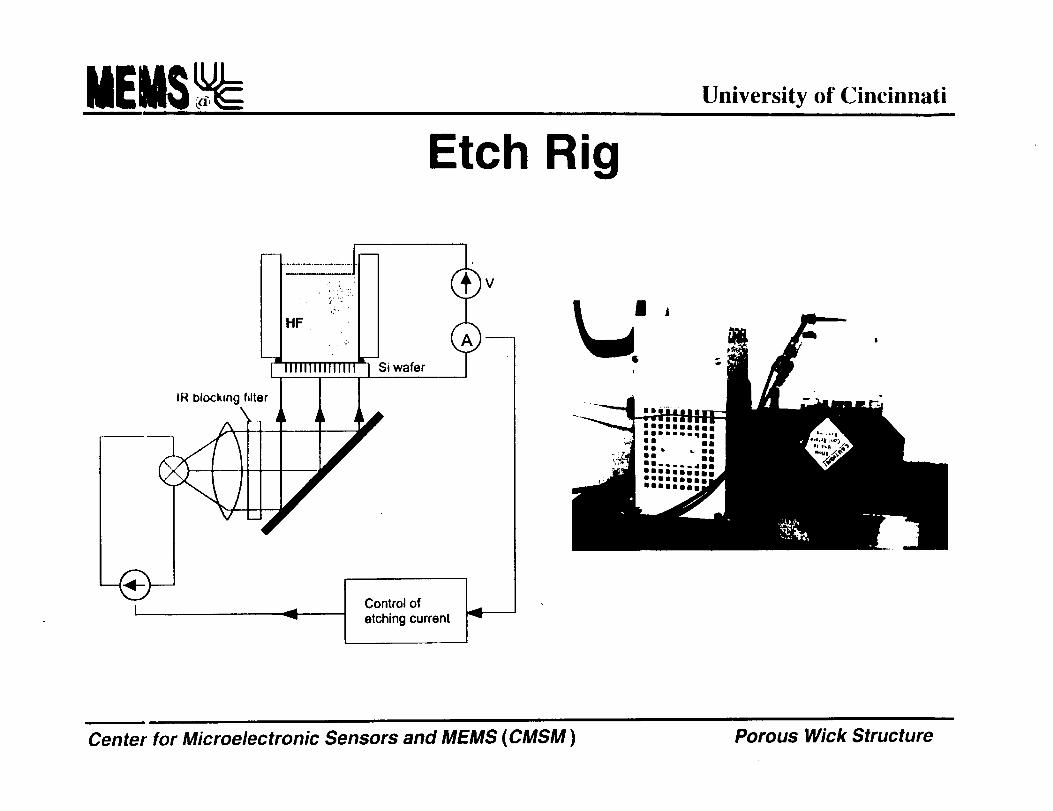
2. Etching System Setup
A new etching system was designed and built from scratch. (See Fig. 16 for
system schematic andFigures 17 and 18 are actual photographs of the system,) We were
able to use some knowledge and experience gained from our electrochemical etch stop
rig, but the inclusion of a light source and other optical parts constituted a new challenge
since HF as the etching solution does etch glass.
The rig was designed for operation in the upright position. This allows the
resulting hydrogen gas to more easily detach from the wafer surface. All the parts in
contact with the HF solution are made of Teflon or other compatible material. Since the
illumination can lead to a temperature rise, a cooling loop was added (not shown),
consisting of tubing, a peristaRic pump and a chiller.
The etching is controlled by a PC and HI' [nsmunents system package (Fig. 18).
A computer program was written which takes the etching parameters as the inputs and
automatically controls the bias and current o_put. It also includes some safety shutdown
features just in case the system experiences My abnormal operating conditions. Finallynote that this system can etch the entire t_o-_nch diameter wafers. This is essential for the
eventual implementation of our thermal apphcation into MEMS systems and is in
contrast to the earlier pioneering work done on extremely small samples by the Munich
group [$1.
23

..............II |lillilllllllll ] Slwafer
Fig. 16: Sketch of etch rig & control loop
Fig. 17: Photograph of light source with etch rig
Fig. 18: Photograph of the PC and HP instruments
24

_licrofabrication o Porous Structures: Preliminary Results and Success
_) Preliminary' Samples: A couple of lessons had to be learned of course, before the
desired pore geometry could be achieved
Fig. 19: Randomly distributed pores (no initiation)
showed that the theory practically works. The etch
depth was fairly predictable and the widening of the
pores was induced by current-voltage curve
experiments.
Fig. 20: Successful pore initiation using a
mask; without IR blocking filter the porestend to branch.
Fig. 21" Etched sample showing that too
high of a doping concentration also leads to
pore branching of a different kind,
25
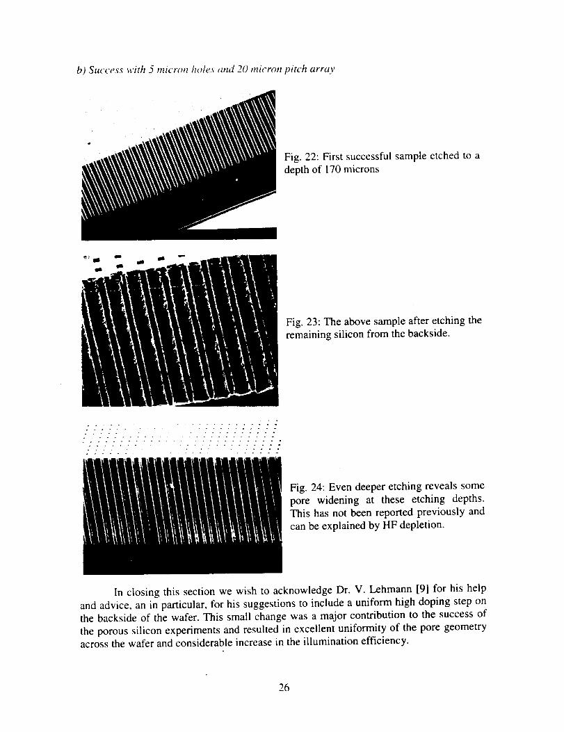
b) Success with 5 micron holes and 20 micron pitch array
Fig. 22: First successful sample etched to a
depth of 170 microns
Fig. 23: The above sample after etching the
remaining silicon from the backside.
................ ;:_
. ; .. ; ? .....- ..... ...... : ?., ..., ? : : :
Fig. 24: Even deeper etching reveals some
pore widening at these etching depths.
This has not been reported previously and
can be explained by HF depletion.
In closing this section we wish to acknowledge Dr. V. Lehmann [9] for his help
and advice, an in particular, for his suggestions to include a uniform high doping step on
the backside of the wafer. This small change was a major contribution to the success of
the porous silicon experiments and resulted in excellent uniformity of the pore geometry
across the wafer and considerable increase in the illumination efficiency.
26

4. Characterization of Porous Wick Properties
a/porostty and permeability: theoretical calculations
The porosity of a porous medium, e, is simply defined as the fraction of the total
volu,,c of the porous matrix that is occupied by the open space [10]. Thus 1-¢ is the
fraction of the medium that is occupied by the solid region. The porosity of our given
porous wick structure shown in Fig. 23 (consisting of 5 micron diameter circular through
holes arranged in a square in-line pattern spaced 20 microns apart) is thus very easily
calculated from the geometry and is e = 0,06. Note that the porosity of the porous wick
structure can be significantly increased by decreasing the spacing between the holes byusing a different, smaller pitch, hole initiation mask.
The permeability K of the porous sample is a measure of the flow conductance of
the fluid-flow through the fluid-saturated porous matrix, and is defined [10-12] according
to Darcy's law by the following equation
where Up represents the v01um¢-averaged flow velocity within the porous matrix. Note
that UP should not be confused with the actual interstitial pore level velocity u, i.e. the
local fluid velocity through the open spaces in the porous matrix, but rather UD is the
representative rP.9.rg._ macroscopic space-averaged velocity through a "sufficiently large"
volume of the porous matrix containing both the solid and open regions.
Thus, the permeability, K, can be thought of as the macroscopic manifestation [ 12]
of highly viscous flow through the network of pores in the permeable structure, and as
such its specific value depends on the resulting internal flow arrangement within that
porous matrix. In general since the flow patterns created within most common types of
porous medium are highly complex three-dimensional flows, the permeability constant
appearing in Darcy's law il usually empirically derived in most situations.
However, for some very well-defined, simple, and repetitive porous structures of
known geometry (such as the porous wick structure under investigation as shown in Fig.
23) the permeability can also be obtained from the application of the first principles of
flow of viscous fluids at the pore level (ie. viscous flow in tubes). Again, it should be
emphasized that this approach is not feasible for very complex and irregular geometries,
but only can be applied for very simple geometric structures. In short, it can be said that
no single, overall _ relationship exists between the pore structure and permeability;
the few existing empirical, semiempirical, and first principle-based correlations all have to
be used within the restrictions for which they have been developed.
27

Fortunately, for the case on hand, since the porous wick struc*ure is composed of
a well-defined small-scale network of straight channels, it is therefore possible to
theoretically derive its permeability as a function of pore size and pore spacing from first
principle using viscous flow theory. To this end the flow through each tube (i.e. pore level
modeling) is modeled as laminar fully-developed Hagen-Poiseuille flow. (The laminar
fully-developed assumption is reasonable due to the anticipated very small pore Reynold
number, Red - O[1], and due to the rather large L/D = 250/5 ratio.) Recalling from fluid
mechanics [12], fully-developed laminar flow in a round tube of radius r o is governed by
(16)
Solving thisequation subjectto u = 0 at the cross-sectionperiphery(r = ro ) yields
or (17a, b)
where u is the actual local fluid velocity, i.e. u(r), and U is the average or mean fluid
velocity integrated across the channel (pore) cross-section.
Now considering once again the entire porous wick structure (global modeling)
and assuming thatDarcy law isapplicable,which isa very validassumption for slow flows
in porous media, the flow when analyzed as passing through the porous medium as stated
earlierisgoverned by the followingequation
u D= (18)k Ox)
where UD is the representative _ l_olume-average) fluid velocity. In terms of the
average fluidvelocityin a singlechannel. U. and takingintoaccount the pore densityof
the porous sample, letN/A be the number of pores per unitfrontalar_ (tubes/m2) and
where A isthe total(open and solid)fronud acea (m2), the porous fluidvelocitycan be
expressed as
25

(19)
and ,,,kfich is simply equal to UP = eU when one recalls the earlier definition of porosity.
Combining Equations (IT o) - (19) one finds
(20)
rearranging, permeability is then
NK : : _-s (21)
8 A 8
Equation (21) gives a relation between the permeability and the porosity for. our givenporous wick geometry based on the previous assumptions of fidly-<leveloped laminar flowand Darcy's law.
Figure 25 is a plot of the permeability as a function of the pore size for a given
pitch pattern based on the above theory. As shown, the smaller the pitch, the higher the
permeability of the porous wick for a given hole size. Smaller pitch means the holes are
spaced closer together and thus there are a greater number of holes for fluid flow in a
given cross-sectional area and thus less flow resistance. And, for a given fixed hole pitch
pattern, we see that the permeability increases with hole size up to a maximum value
limited by when the individual holes merge, i.e. the pore diameter equals hole pitch for this
inline arrangement. Here, larger holes again mean more flow area (and higher porosity),
therefore less flow resistance and thus higher permeability.
The dotted line in Fig. 25 is the empirical results taken from the latest U.S. and
Russian research [13] in sintered power metal wick fabrication and is shown here for the
sake of comparison. The plotted correlation is a curve fit of aotual permeability
measurements representing the "state-of-the-art" in porous wick fabrication using
"advanced" fine pore processing technique ._though the theoretical permeability of our
very first successfully micromachined porous sample (solid symbol, 5 micron dia. holes
with 20 micron pitch; K- 1.0E-14 m2) is shghtly less in magnitude than the best that is
currently available, this figure clearly re_eals the great potential to easily exceed the
current limitations by simply micromachmmg smaller size holes packed closer together.
29

iI-o2
t 1-14
I _.00
I OaE 10
20 i_mhl
i_ SmrnhotN _ 20pmtl_l=h
,.°.. .o-r .......' Pitch = 1gin .....
o-°'°'°'°'°'''" "° ,
! 7 __ "__. Ruuian Pore wick,
1 OaI -,10 J
t 147 t 001.41 tI_ I I_
po_ Radlue,r. [m]
Figure25 -Theoreticalpermeabilityofthemicromachinedporouswick structureasa
functionoftheselectedporeradiusand pitchwithcomparisonto current
state-of-the-artwick technology
b) porosity and permeabilzty: e_erimental testing
Porosity of the porous sample are to be determined two ways. First, the porosity
of the porous sample can be easily calculated from its definition given the exact geometryof the holes. The rep_tive pore size and pore hole distribution measurements are
obtained from close up photographs taken under the microscope of the porous sample atdiscrete locations. Circular holes and a repetitive pattern is assumed to extend throughout
the entire porous specimen and any nonuniformity in the individual pore hole or in the
pore distribution pattern will result in some inaccuracy in the porosity calculation.
However, judging fi'om the excellent pore uniformity obtained in the successfully
fabricated porous sample (Fig. 23) we feel that the slight deviations in shape will cause a
relatively small error in the porosity calculation. Second, it is also possible to the
determine the porosity of the porous sample by weight analysis by using a very sensitive
3O

mass scale if the overall dimensions of the porous sample are known. The advantage of
this method is that the exact internal pore structure does not have to be measured to use
this technique. However, the uncertainty in the weight measurement and the uncertainty in
the overall sample's dimensions are the major source of errors to consider when measuring
porosity using this second methodology.
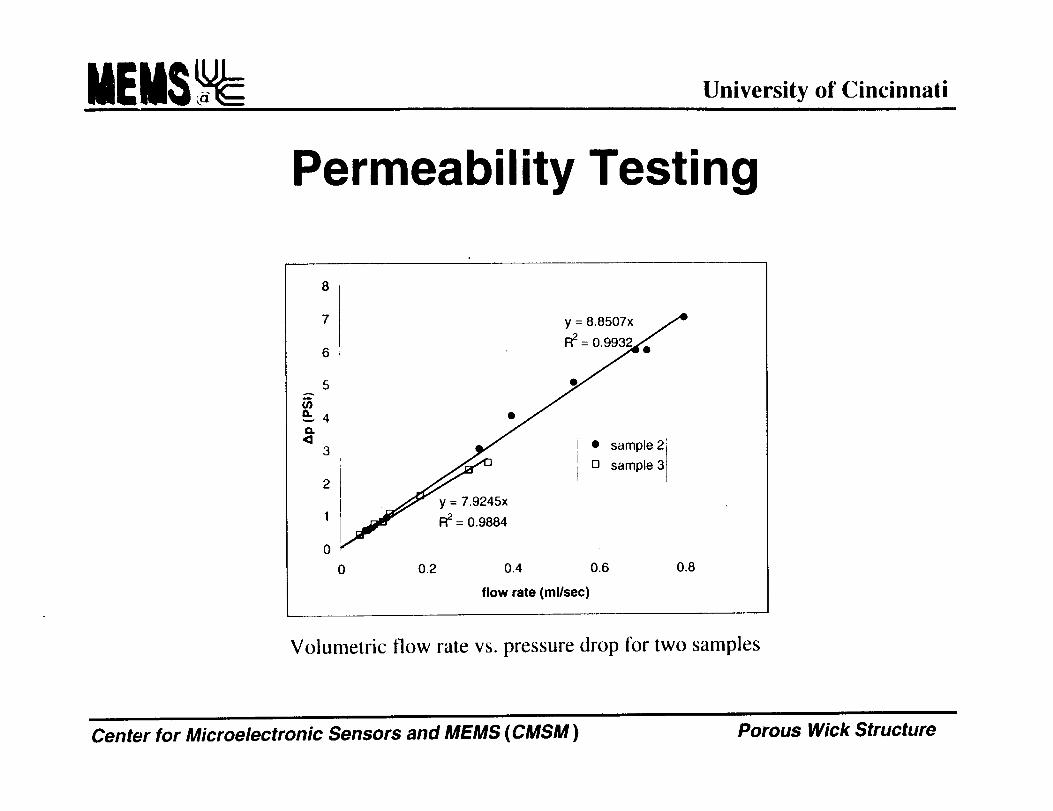
The sample permeability can be determined if the fluid flow through the wick and
the resulting pressure drop across the wick are known, recall Darcy's law, Equation (15).
These quantities are to be experimentally measured using our fluid flow testing loop
facility shown below in Figure 26. Note that this flow circuit is essentially the same water
testing loop facility used in the previous microchannel cooling experiments [5] i.e. the
same pump, instrumentation, etc., but has been slightly reconfigured with a new test
section (see insert) specifically designed to securely hold the porous sample in line with the
water flow. The pressure drop and fluid flow rate are to be measured electronically using a
pressure transducer and turbine flow meter, respectively, and the data recorded using the
PC and data acquisition system. We have just successfully completed "leak testing" the
new test section and are now ready to begin permeability testing of the porous samples•
(See section IVB.2 for further details•)
I
Figure 26 - Porous wick permeability testing loop; insert shows close-up of test section
31
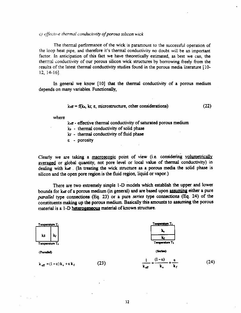
c) effectlve thermal condttclivtty of porous stlicon wick
The thermal performance of the wick is paramount to the successful operation of
the loop heat pipe, and therefore it's thermal conductivity no doubt will be an important
factor. In anticipation of this fact we have theoretically estimated, as best we can, the
the .rm.._ conductivity of our porous silicon wick structures by borrowing freely from the
results of the latest thermal conductivity studies found in the porous media literature [10-
12, 14-16].
In general we know [10] that the thermal conductivity of a porous medium
depends on many variables. Functionally,
where
k_r = f(la, kt, s, micrormacture, other conaiderations)
kea"- effective thermal conductivity of saturated porous medium
Io - thermal conductivity of solid phase
ks - thermal conductivity of fluid phase
¢ porosity
(22)
Clearly we are taking a macroscopic point of view (i.e. considering vol_tmetrically
averaged or global quantity, not pore level or local value of thermal conductivity) in
dealing with k_. (In treating the wick structure as a porous media the solid phase is
silicon and the open pore region is the fluid region, liquid or vapor.)
There are two extremely simple I-D models which establish the upper and lower
bounds for k_ of a porous medium (in general) and are based upon _ either a pure
parallel type connections (Eq. 23) or a pure series type connections (Eq. 24) of the
constituents making up the porous medium. Basically this amounts to assuming the porous
material is a I-D hlffdlIflg.q_9_ material of known structure.
Tnmpetlnn_ T i
Tm,wemmmmT_
T_ T,
It.
kfT_TI
1 (1-6) s (24)kar =(l-_-)k, +¢k t (23) ken. k, k t
32

Often however, porous material is composed of packed beds of particles and as
such contains a combination of both types of heat transfer paths (series and parallel).
Empirically this arrangement has been shown to behave according to
kar = k_l-c)k_ (geometricmean) (25)
as long as ks is not two much different than k.,, with the value of k_c falling
somewhere in between the two limits just described. Also note that regularly or randomly
packed beds to a very good approximation can be treated as a homogeneous medium with
respect to the effective thermal conductivity, i.e. no directional dependence.
More accurate formulas for kar are available in the literature but become
increasingly more complex, requires additional information, and are more "system
specific" applicable to a particular type of porous medium. For example, better
correlations exists (based on 2-D and 3-D models) specific for a given particle geometry
(spheres,rods, etc.)with known packing arrangements (simplecubic,body centercubic,
etc.).Also, ifpacking israndom but tend to take on a certaindistribution,let'ssay four
differentkinds of packing structures,a _ of karcan be theoreticallypredictedbased on
the probabilitydistributionof findingthose certaintypes of packing structureswithin the
porous medium. Equations (26)-(27)listedbelow isof thislasttype and gives the upper
and lower bounds forthe traverseconductivityk_n, for a two-dimensional anisotropic
fibrousmaterialcomposed of needle-shaped fibers,allbeing arranged in parallelwith each
other,ina gaseous or solidmatrixof differentthermal conductivity[14].
t L12II+a,c8-l)l
(Upper limit) (26)
0Lower limit) (27)
s_/here
8. = t - s _ = k___, G=0,25 for Circle shaped cellskf
Note that tim recommended effective therrrud conductivity (according to reference [14]) in
the _ direction (parallel to the fibers) tot the same anisotropic fibrous porous medium
structure is simply given by the earlier Eq t23) Hence, to summati_ for this stated
fibrous arrangement it's concluded [14] ,,hat the very simple parallel I-D model is
reasonable for predictingk_ui,_ but the k,n.,_,_= values range somc_vhem between the
upper and lower 2-D limitsas given by Eqs (26) and (27),respoctively(whicharesignificantlylargerin magnitude than the l-IDseriesmodel estimate of F_,q.124) due to
multi-dimensiomd heat conduction inthe medmm )
_3

These different thermal conductivity models just described are ,Jsed to estimate the
effective thermal conductivity of our porous silicon wick structure, saturated with water in
Table 1, and saturated with water-vapor in Table 2, for select values of porosity. The
results of the wick saturated with water is also shown plotted in Figure 27 Inspection ofTables I-2 along with Figure 27 reveals the following:
i) rhe value ofk_rofthe wick structure saturated with water or saturated with water-
vapor is approximately the same for kat,,a., (Eq. 23), kate,,,,,, u_ timit (Eq. 26), and
kc_s,,om,._c ,ram (Eq. 25) models, i.e. compare the values of Table 1 and Table 2, but
differ significantly for k_ n_m k,,,_ timit (Eq. 27) and _ (Eq. 24) models.
2) k_ _ (Eq. 23) varieslinearlywith porosity(thusisa strongfunctionofe)_
3) k,.a; u.,v,m 2-D upper and lower limits, Eqs.(26) - (27) >> ic,n;t-O _ Eq. (24).
(Hence the I-D series model greatly underestimate the value of k_u,,,,m). Also note
that k_v._ dependence on porosity diminishes as 8 increases, now dominated by the
value of the low conductivity fluid).
4) ka_s,,,_,_a¢ _ Eq. (25), is always within the upper and lower bounds of k,n;u,,,,,w
and is a much simpler equation to use to calculate the effective thermal conductivity.
5) k_,._ > k_nw 2.o_t forallvaluesof porosity.
In applying the above results to the wick geometry there are two additional facts that one
should keep in mind:
6) The wick geometry is not exactly the same as that of the 2-D fibrous insulation
system modeled and analyzed in ref. [14]; however both systems are reasonably similar
in shape to one another to a certain degree, note also that ref. [ 14] geometry is the
closest that can be found to the wick structure in the literature without doing a more
extensive search.
7) The results of reference [14] is based solely on a theoretical study only and was not
validated experimentally at the time (although latter reference to this study imply that
the reported results are reasonable.)
Hence, given these last two comments imply that one should use caution in applying the
results of Eq. (23) and F,qs.(26)-(27) (or Eqs (23) and (25)) to determine ha.m_ and
k_, respcctive, ly, of the porous silicon wick. The results obtained using the above
equations therefore should be viewed only as rough estimlLtes 9ul_, not actual values of
the effective thermal conductivity of the porous wick structure. Finite element modeling
[16] are recommended (and/or actual thermal conductivity testing of the wick is
suggested) if more precise values of thermal conductivities of the wick structure are
needed. (However we do feel that the equations listed above reveal the proper trends, i.e.
effect of porosity, thermal conductivity of the saturating fluid (water vs. water-vapor)
directional dependence (axial vs. traverse), etc, and, in fact, can provide reasonable first
cut estimates.)
34

Table 1 K.-1211W/m"C
Porosity Eq. 23
0.2 102.5300.5 84 314C.7 38.8400.9 13.380
Kr-O.(N,II W/m °C
Eq. 24 Ecl.253.176 44'.4721.289 9.1070,924 3.1840.720 1.099
Table 2 1(,,,1211 W/m "C K_24.1x10 4
Porosity Eq. 23 Eq, 240.2 102.405 0.1230.5 64.012 0.0490.7 38.417 0.0350.9 12.822 0.027
v/m'q¢
Eq. 2523.1181.7740.3200.058
Silicon I W_er
Eq. 2682.35932.80712.3792.037
Ec[.2713.9462.5281.3090.798
|illccm I Wltlr-VlllOq
Eq. 26 Eq. 2781.937 0.61132.031 0.09811.553 0.0501.309 0.030
J
120
gO
60
]0
/ . k,a._ (Eq.23)
,/',.
02 04 06 0.11 IPoremia_r,=
Fig. 27 Thermal conductivity (theoretical) of the micromachined silicon porous wickstructure saturated with water as a function of porosity
" 35

IV. PLANNED _,ORK (Year 3 Goals)
B. Porous Wick Structure
1. Microfabrication of Porous Silicon _ ick Structures
Our goal next year is to fabricate a second set of porous silicon test specimens,
again with straight through holes, but th_s t_rne the pores fabricated in the silicon wafer
will be smaller and spaced much closer together In particular, additional pore initiation
masks will be fabricated which allow for pore arrays with a 4-micron pitch. This is at the
lower limit of our photolithography equ,prnent Both linear and staggered pore arrays will
be made and the pore diameter will be reduced to about 1 micron in these samples.
The slight widening of the pores as observed in our earlier results (Fig. 24) will
also be investigated and studied. We will control this behavior in our earlier 5-micron
diameter pores samples by adjusting the light intensity. Then, if necessary, it will also be
dealt with accordingly in the latter samples containing the smaller hole arrangements.
Since this effect has not been previously reported in the literature our findings may result
in a short publication.
The fabrication of a porous silicon wafer with the much finer pore patterns will
essentially conclude the macro porous silicon fabrication efforts here at UC, although itneeds to be stated that much more work still remains to be done before a rnicromachined
silicon porous wick can be successfully integrated into a loop heat pipe. (See section B.3
for further discussion.)
2. Testing of Porous Silicon Samples
The porosity and permeability of the porous silicon samples with be measured here
at UC using the techniques and test set-up as described in section III.B. 4.b. Testing of the
5 micron pore sample is currently in progress; the smaller pore samples will also be
similarly tested when available. It is our hope that the measured permeability will closely
follow the theory but any major deviation in the data from theory will be resolved.
Thermacore and Texas A&M are expected to confirm our results by doing repetitive
testing on similar samples (fabricated by UC) using their own testing facilities. The
effective thermal conductivity of the samples will not be measured.
3. Microfabrication of Advanced Porous Structures
- As mentioned in the Project Description section, there may be some advantage to
varying the pore diameter across the thickness of the wick. This should allow one to
operate under normal conditions with one radius of curvature, and utilize another radius of
curvature to prevent the meniscus from receding into the liquid. Also, by shortening the
length of the smaller diameter section, the hydrostatic pressure drop can be reduced.
Several discussions have occurred between the University of Cincinnati, NASA
Lewis, DTX and Texas A&M. Two or three concepts have been proposed. Before any
final design, however, DTX and Texas A&M will have to perform some detailed
calculations to specify the actual dimensions which are desired. The University of
Cincinnati can then determine.if it is possible to fabricate. Of course several iterations may
be necessary before a workable design can be reached
44

V. CLOSLNG
Although many multi-chip module (MCM) approaches have been tried or used in
recent years, the one herein proposed is quite revolutionary, but yet realistic. Work is
progressing at a steads rate on schedule and major achievements have already been
realized at this point in time. Ultimately, the micromachined integrated MCM thermal
management system should demonstrate that the chip temperatures can be maintained at
the present levels while increasing the volume density by as much as two orders of
magnitude at the chip level. The resulting savings in mass and volume we feel will prove
to be extremely beneficial to NASA.
m m
Also, an additional endeavor that is to be accomplished during the course of this
project is to use MEMS technology to fabricate "porous" silicon, with specific
"micromachined" geometric characteristics, to form the ultimate in wick structures for use
in heat loops. To the best of our knowledge porous silicon has never before been
considered for such a thermal application but has rather been investigated for its
luminescent properties (not fully understood). However, since the porosity, anisotropy
and pattern configuration can be controlled it could revolutionize the area of
semiconductor cooling, thermosyphon evaporation, etc. Moreover, the planar technology
is a batch-processing technique, which will ultimately be very inexpensive.
Of course successful creation of porous silicon wicks will be of great benefit for
utilizing this MCM concept in space applications. Eliminating the piamp will further
reduce the mass and volume of the complete thermal management system.llD
Thus, we feel that this project embodies several rather revolutionary and potentially
very pragmatic areas of thermal development by cross-fertilization of several disciplinary
areas heretofore overlooked.
.t6
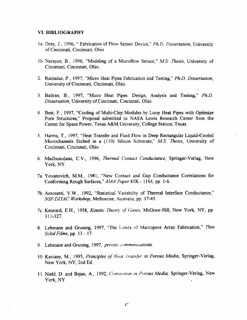
VI. BIBLIOGRAPHY
l a. Doty, J., 1996, " Fabrication of Flow Sensor Device," Ph.D. Dissertation, University
of Cincinnati, Cincinnati, Ohio.
lb. Narayan, B., 1996, "Modeling of a Microflow Sensor," M.S. Thesis, University of
Cincinnati, Cincinnati, Ohio.
2. Ramadas, P., 1997, "Micro Heat Pipes Fabrication and Testing," Ph.D. Dissertation,
University of Cincinnati, Cincinnati, Ohio.
3. Badran, B., 1997, "Micro Heat Pipes: Design, Analysis and Testing," Ph.D.
Dissertation, University of Cincinnati, Cincinnati, Ohio.
. Best, F., 1997, "Cooling of Multi-Chip Modules by Loop Heat Pipes with Optimize
Pore Structures," Proposal submitted to NASA Lewis Research Center from the
Center for Space Power, Texas A&M University, College Station, Texas.
, Harms, T., 1997, "Heat Transfer and Fluid Flow in Deep Rectangular Liquid-Cooled
Microchannels Etched in a (110) Silicon Substrate," M.S. Thesis, University of
Cincinnati, Cincinnati, Ohio.
6. Madhusudana, C.V., 1996, Thermal Contact Conductance, Springer-Verlag, New
York, NY.
7a. Yovanovich, M.M., 1981, "New Contact and Gap Conductance Correlations for
Conforming Rough Surfaces," AIAA Paper 81K - 1164, pp. 1-6.
7b. Antonetti, V.W., 1992, "Statistical Variability of Thermal Interface Conductance,"
NSF/DITAC Workshop, Melbourne, Australia, pp. 37-45.
7c. Kennard, E.H., 1958, Kinetic Theory of Gases, McGraw-Hill, New York, NY, pp.
311-327.
8. Lehmann and Gruning, 1997, "The I_imlts of Macropore Array Fabrication," Thin
Solid Films, pp. 13 - 17.
9. Lehmann and Gruning, 1997, private _Jmmumcations.
10. Kaviany, M., 1995, Principles of tteat lran._fer in Porous Media, Springer-Verlag,
New York, NY, 2nd Ed.
11. Nield, D. and Bejan, A., 1992, ('om'ect,m m t'orous Media, Springer-Verlag, New
York, NY.
47
12. Bejan, A., 1984, Convection Heat Transfer, John Wiley & Sons, New York, NY.
13. Gernert, N, Baldassarre, G., and Gottschlich, J., 1996, "Fine Pore Loop Heat Pipe
Wick Structure Development," Proceeding of Aerospace Atlantic Conference, SAE
paper # 961319, pp 1-10.
14. Tien, C. and Vafai, K., 1979, "Statistical Bounds for the Effective Thermal
Conductivity of Microspheres and Fibrous Insulation," Prog. Astronaut. Aeronaut. 65,
135-148.
15. Nield, D.A., 1991, "Estimation of the Stagnant Thermal Conductivity of Saturated
Porous Media," Int. J. HeatMass Transfer, Vol. 34, No.6, pp. 1575-1576.
16. Bakker, K., 1997. "Using the finite element method to compute the influence of
complex porosity and inclusion structures on the thermal and electrical conductivity,"
lnt. J. HeatMass Transfer, Vol. 40, No. 15, pp.3503-3511.
48

APPENDIX B


olEII
WoimU
olemm
l
iim,4..I
oNomu
aim
omCO
)
.._
II
iimn-
_Lv

i
._0
_,
0,
,0
,,
'n_
_g
{nI

eml
_mJ
*m*m
em*
¢.)
XEU')
E--'7.
:3U)
c_r_

amWomeaU
om_P_
0nm
CO
)c_
•n_C
,)m
inIi
T"
G)
olmOE=L
.
×E°_"L
×=L
.
_3
Ac_I,,,
c_

Im
=
C_
om
Theoretical Permeability Development
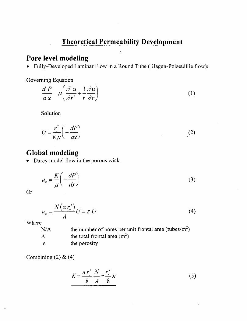
Pore level modeling• Fully-Developed Laminar Flow in a Round Tube ( Hagen-Poiseuillie flow):
Governing Equation
dP (_u lcTu'_
) (1)
Solution
U __. O (2)
Global modeling• Darcy model flow in the porous wick
Or
(3)
u,, - U = c U (4)A
Where
N/A
A
E
the number of pores per unit frontal area (tubes/m 2)
the total frontal area (m 2)
the porosity
Combining (2) & (4)
__
1 2
zcr N r-- ,9
8 A 8(5)

==om=omr_
oU
m•gin
=_EI.=
0..
,,,,,
t
Q
__
I_m__
I__
!
-______
!,
c,a
IIl_
a
0I
111
t'-vP
+"Ei._O
)O
.
i11
I
i,i

Summary
microchannels and milli-slot have been
fabricated, tested and thermal model verified
• prototype MCM module with micromachined
pockets and chips has been fabricated
3-D thermal model of MCM module is under
development
• contact resistance experiments, 3-D chips-to-
substrate, are almost ready to begin
• 5 ._tm holes x 20 _tm (pitch) silicon porouswicks have been successfully fabricated
• permeability measurements of porous wick
test specimens are ongoing
• 1 _tm holes x 4 _tm (pitch) silicon porouswicks are under fabrication
• future work

APPENDIX C

Coherent Macro Porous Silicon as a Wick Structure in an Integrated
Microfluidic Two-Phase Cooling System• .a • h
Alcxandcr D. Hrlke", Jbrg Ptlchowskl , H. Thurman Henderson", Ahed Saleh h, Michael Kazmmrczak ,Frank M. Gerner _', Karl Baker c
"University of Cincinnati, Center for Microelectronic Sensors and MEMS (CMSM), P.O. Box 210030,
hUniversity of Cincinnati, Dept. of Mech., Ind. and Nucl. Eng
'NASA Lewis Research Center Cleveland, Ohio
ABSTRACT
This paper reports a new concept of building a coherent porous wick structure in planar silicon wafers for capillary pumpingin Loop Heat Pipes (LHPs). By utilizing Macro Porous Silicon (MPS) fabrication technology, with pore sizes in the order of
a micron, precise control of the pore dimensions of the wick is possible. In addition, by using MEMS (Micro ElectroMechanical Systems) fabrication technology, LHPs can ultimately be integrated into electronic packaging systems, or indeed
into the silicon microchips themselves. The MPS samples were fabricated and tested for capillary pressure and permeability.The test results closely matched the analytical models that were derived from basic physics.
Keywords: Macro Porous Silicon (MPS), Loop Heat Pipe (LHP), wick, electronic cooling, microchannel flow
I. INTRODUCTION
Enhanced cooling of present and next generation electronic packaging systems is crucial. The realization of increased speedand higher device density result in ever-higher heat fluxes, calling for design of fully integrated packaging-cooling systems.
This work reports a portion of a larger ongoing effort to develop a unique all-silicon MCM (Multi Chip Module) design [1]which includes several concurrent cooling schemes, such as forced liquid cooling in ultra deep microchannels [21, passive
cooling with Loop Heat Pipes (LHPs) and more traditional air fan cooling. The passive nature of the heat pipe operationrenders them particularly attractive, since no external driver is required. The porous wick in the device is itself the pump of
the LHP, using only the very heat it removes.
First, this paper covers heat pipe and LHP fundamentals and the particular importance of the wick. Then, the characteristic
parameters of capillary pressure and permeability are introduced and applied to the coherent wick. Macropore fabrication isincluded with particular attention paid to the necessary and important fabrication details. The testing results are then
compared to the theoretical predictions. Finally, an integrated evaporator concept for MCMs is introduced.
2. COHERENT WICK DESIGN
Motivation
A heat pipe is a sealed device in which a workingfluid circulates and constantly changes from the
liquid to the gaseous phase, and vice versa(Figure 1). The evaporated liquid flows from the
evaporator to the condenser end by the pressure
drop created from the evaporation andcondensation process. The liquid is returned to
the evaporator by the capillary pressure in thewick. The input heat energy is thus convertedinto latent heat in the evaporator, moved in the
gaseous phase to condenser, and then convertedback into heat energy by the evaporation process,and the heat is then ejected at the condenser end.
The evaporation and condensation process takes
heat sink heat source
A liquid flowq
Ap,bqu_ -- T: evaporatorcondenser (wick)
TH TL
vapor flow
Figure I. The basic cycle of a heat pipe.

placeatalmostthe,;ametemperature,i.e.it isvirtuallyisothermal.Ina2Danalogy,oneoftencompare_,aheatpipe_,ithahighlythermallyconducti'_ematerial.Thefiniteheatfluxq is transported at a small temperature difference AT, resulting in a
high effective thermal conductance G,,.,+,:
q --+_ II)G,,,,, = [_ _,_,,
Heat pipes offer a passive way of rapidly transporting energy away from a heat source. The term "'passive" is used here in thesense that no external action, such as pumping, is required for operation. The heat itself pumps these devices. This has certainadvantages over other heat removal techniques. No extra devices (such as pumps or other actuators) are needed, and no
additional power needs to be introduced as heat into the system.
The distinction between an ordinary heat pipe (HP), where a wick continuously lines the inner surface of a single pipe, and a
capillary pumped loop (CPL) is that in a CPL interconnecting plumbing separates the condenser and evaporator (including
the wick). The length of an ordinary heat pipe is limited, because the whole liquid return path is through the wick, whichresults in high viscous losses. The capillary pumped loop overcomes this shortcoming, but it is not inherently self-starting.
A recently developed type of heat pipe is the Loop Heat Pipe (LHP) [3]. It is similar
in design to a Capillary Pumped Loop because it uses separate tubing for the liquidand vapor flow paths, which allows the thermal energy to be moved over relativelylarge distances (Figure 2). The wick is located at the evaporator and it serves as the
engine, which achieves continuous circulation. The LHP is unique because theoverall design provides for a reliable start;up. Working LHPs have been made using
cylindrical and planar evaporator configurations.
The porous wick is without question the most important part of a LHP. It transfersthe energy to the liquid-vapor interface ("meniscus") and maintains separation
between the vapor and the liquid by capillary forces. The porous wick thusdetermines the pumping capability of a LHP like no other part. MEMS (MicroElectro Mechanical Systems) technology opens up new possibilities in wick design,
as well as modeling. Traditional, sponge-like porous wicks have a randomlydistributed pore size, and the flow path is irregular. Consequently, the mathematical
description is statistical and semi-empirical. On the other hand, the coherent natureof wicks fabricated by the Macro Porous Silicon (MPS) etching technique allows a
relatively simple analytical description of the parameters.
Capillary Pressure
LiquidReservoirs
LiquidLine
Evaporator
_Wick
i qi: Heat
L VaporLine
_ Condenser
Figure 2. Schematic of a Loop HeatPipe, redrawn from [3]
The capillary action pumps the liquid from the condenser to the evaporator. The capillary pressure has to overcome all otherpressure losses in the system. Wetting and surface tension result in a curved liquid surface, or meniscus. Macroscopically, the
pressure drop AP, across the meniscus is described by the surface tension a, the wetting angle ®, and the pore radius r, [6]:
20 cos 0AP. - (2)
r;Practically, one often introduces an effective surface tension, acos®, since it is difficult to separate the two components in
boiling experiments. In order to achieve a high capillary pressure, a small pore radius, good wetting and a liquid with large
surface tension are required.
Permeability
The permeability K is a measure of the liquid flow conductance through the porous wick. It is used in the expression
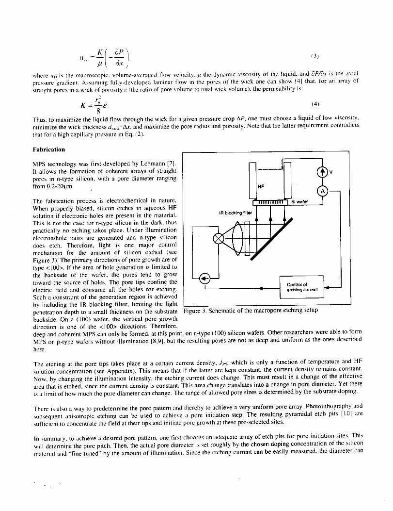
ut ) =-- - (3)p 3x j
where tit) is the macroscopic, volume-averaged flow velocity./.¢ the dynamic viscosity of the liquid, and _P/&_ is the axial
pressure gradient. Assuming fully-developed laminar flow in the pores of the wick one can show [4] that. for an array ofstraight pores in a wick of porosity e (the ratio of pore volume to total wick volume), the permeability is:
2
K = rt' £. (4)8
Thus, to maximize the liquid flow through the wick for a given pressure drop AP, one must choose a liquid of low viscosity,minimize the wick thickness d_,,,=Ax, and maximize the pore radius and porosity. Note that the latter requirement contradicts
that for a high capillary pressure in Eq. (2).
Fabrication
MPS technology was first developed by Lehmann [7].It allows the formation of coherent arrays of straight
pores in n-type silicon, with a pore diameter rangingfrom 0.2-20_m.
The fabrication process is electrochemical in nature.
When properly biased, silicon etches in aqueous HFsolution if electronic holes are present in the material.This is not the case for n-type silicon in the dark, thus
practically no etching takes place. Under illuminationelectron/hole pairs are generated and n-type silicon
does etch. Therefore, light is one major controlmechanism for the amount of silicon etched (see
Figure 3). The primary directions of pore growth are oftype <100>. If the area of hole generation is limited tothe backside of the wafer, the pores tend to grow
toward the source of holes. The pore tips confine theelectric field and consume all the holes for etching.
Such a constraint of the generation region is achieved
by including the IR blocking filter, limiting the lightpenetration depth to a small thickness on the substratebackside. On a (100) wafer, the vertical pore growthdirection is one of the <100> directions. Therefore,
[ ummm,,n ],_wafer
trol of
[ = etching current
Figure 3. Schematic of the macropore etching setup
deep and coherent MPS can only be formed, at this point, on n-type (100) silicon wafers. Other researchers were able to formMPS on p-type wafers without illumination [8,9], but the resulting pores are not as deep and uniform as the ones described
here.
The etching at the pore tips takes place at a certain current density, JPs, which is only a function of temperature and HFsolution concentration (see Appendix). This means that if the latter are kept constant, the current density remains constant.
Now, by changing the illumination intensity, the etching current does change. This must result in a change of the effectivearea that is etched, since the current density is constant. This area change translates into a change in pore diameter. Yet there
is a limit of how much the pore diameter can change. The range of allowed pore sizes is determined by the substrate doping.
There is also a way to predetermine the pore pattern and thereby to achieve a very uniform pore array. Photolithography and
subsequent anisotropic etching can be used to achieve a pore initiation step. The resulting pyramidal etch pits [10] aresufficient to concentrate the field at their tips and initiate pore growth at these pre-selected sites.
Ii1 summary, to achieve a desired pore pattern, one first chooses an adequate array of etch pits for pore initiation, sites. This
will determine the pore pitch. Then, the actual pore diameter is set roughly by the chosen doping concentrauon of the siliconmaterial and "'fine-tuned'" by the amount of illumination. Since the etching current can be easily measured, the diameter can

be accuratcl.,, controlled. Small changes in pore diameter are possible within the range allotted by the doping constraint.
Finally, the pore tip etches _ith an etch rate that is proportional to the current density J_,_.Thus. the desired pore depth isachieved by timing the etching process.
The etching, howc_er, cannot quite continue through the whole wafer thickness because of two reasons: (1) The pores atsome point cannot grow towards the source of holes as they etch into the generation region, because the field confinement of
the pore tips is not effective any longer. Thus, as the pores approach the broad backside field plane, they tend to branch. (2)The HF would leak out of the setup and damage the optics in our system. Instead of etching pores through the entire waferthickness, the pores are etched through most of the wafer, and then, the wafer is selectively etched from the backside using
TMAH or another appropriate etchant, until the pore region is reached.
Lehmann [7] already pointed out that the etching process leads to an effective decrease in HF solution concentration at thepore tips. resulting in a parabolic development of the pore depth over time. It was found in the present study that this alsoleads to an increase in pore diameter with increasing depth if the etching current is kept constant (Figure 4). Based on the
parabolic development of the pore depth, the concentration change can be calculated and the current can be appropriatelyadjusted (see Appendix). Samples etched with these improved parameters exhibit a constant pore cross-section (Figure 5).
" " " " :o
Figure 4. Cross-sectional view of a sample etched at aconstant current. The diameter increases with
depth.
Figure 5. A sample etched with a current that was
adjusted to yield a constant pore cross-section
(appendix).
Thus far, wicks with pores of about 5-71am pore diameter and a pitch (center-to-center distance) of 20_m were fabricated. Atthe moment, our effort is centered towards fabrication of pores _ ith a smaller diameter (l_m) and a smaller pitch (4_m).

Testingsetup for :Measurement of Permeability and Capillary Pressure
Deionized water was used for the flow r
tests, where the pressure drop across the poroussample was measured using a manometer, andthe flow rate was determined by collecting the
volume of liquid over a certain time duration(Figure 6).
The capillary pressure was obtained using thesame setup. Initially, with only liquid on the
pump side and air on the other side of the porouswick sample, menisci formed at the interface.
The liquid initially did not flow, and pressurebuilds up. Only when the pressure exceeds the
capillary pressure does the liquid begin to flow,and the pressure drop across the sample
decreases suddenly. The pressure falls to thevalue determined by the permeability of thesample. The maximum pressure obtained before
the flow starts is the capillary pressure.
manometer
-fporouswicksample
0.5 ixm filter
reservoir
Figure 6. Testing setup for capillary pressure and permeability.
3. RESULTS
As Eq. (3) suggests, the permeability of the sample can be deducted from the slope in the flow / pressure drop diagram. Forone test run, a line was fitted into the data field (Figure 7) and the permeability calculated. The results of the tests along with
the theoretical predictions, as well as test data from conventional sintered porous metal wicks [4], are plotted in Figure 8.Although permeability data were collected from samples of only one wafer, the results so far confirm the theoretical
predictions. Even with its low porosity (7%), in terms of permeability the coherent MPS wick performs as well as theconventional porous metal wicks (themselves a fairly recent development) which frequently have a porosity value in excessof 50%.
The capillary pressure tests conducted to date are not very precise since the tests were primarily conducted to collect flow
data for permeability measurements (TABLE 1). The additional data shown in the table are measurements taken byThermacore [ I I ] (commercial developer of porous metal wicks) with the so-called bubble-point test. Their results also show
a rather high degree of uncertainty. However, the theoretically predicted radii derived from the measured capillary pressureare also close the SEM measurements.
/
35 20 m_rons Oact_,EqH)/
= 20 mv3ro_18 Olteh,m_,lsure¢l
/ ... •.
3 .... 4 mlcr0¢_ _td_, Eq. {4) . • S-" """
m
/
2.5 ..... _o_ rn_ _. ,,"expe.,v_ [41 /' .._
2
,_ ,/." .....
1 "" '
05
0 F '" - ............
.°. -'"1. t
/
' E _7 1 E-06 E :5
m_u= (m)
I _,_'urc _ Permeability vs. pore radius for two different pore
initiation patterns (masks), as well as conventionalporous metal wicks. The theoretical and test re,,ultsmatch well.
y = 7,9243x •
J • repeat ,
0 0.1 0.2 0.3 0 4
flow rate (mV_)
Figure 7. Example of a flow rate versus pressure drop tc,tThe slope is inversely proportional to the
permeability.

TABLEI.Capillarypressuretestresults
lest l.ah
Uni,..ofCincinnati
Thermacore
fill
Waterl
PS20
PSI7
r,,,,,,(pro)(from SEM)
3.25
2.5
fluid
water
acetone
Test #
I
5 16
7
8
Ap Ipsi) r,,,,_(pro)I from Ap)
6 - 8 2.6 - 3.5
1.17 2.825
1.27 2.6
1.55 2.225
1.41 2.44
4. INTEGRATION
The coherent MPS wick must be ultimately integrated into a working LHP. This would be necessary to clearly demonstratethe feasibility of using a MPS wick.
Anisotropic etching and wafer bonding techniques can be used to create a flat evaporator (Figure 9). On the vapor side,
energy is conducted to the wick by an array of mesas from the hot plate. This plate is anisotropically etched from a (100)silicon wafer using KOH and appropriate corner compensation techniques. The volume between the mesas provides thevapor flow path. This hot plate could be attached directly to an MCM, or be itself part of the all-silicon MCM [ I ]. The porous
silicon plate and the bottom plate form part of the liquid reservoir.
.,, , , ,,,( " \..,..,..
liquid inlet
./-- Hot Plate (HP)
vapor outlet
"- Porous Wick (PW)
Bottom Plate (BP)
Figure 9. Cross-sectional view of an evaporator fabricated by MEMStechnology.
This integrated planar evaporator will replace the conventional, cylindricalevaporator of a working LHP. It is extremely important that the evaporator is
flat for MCM cooling applications, and so far conventional porous metalwicks could not achieve this goal because only cylindrical evaporator sections
have been made. Ultimately, in the future it is envisioned that a whole LHP isfabricated by MEMS (Micro Electro Mechanical Systems) technology.
5. CONCLUSIONS
MPS was used to create a new type of wick for use in LHPs. The gooddimensional control of pore size and pattern offered via state-of-the-art
MEMS-based micromachining allows optimal fine-tuning of the wick'sparameters, such as permeability and capillary pressure. The feasibility of
thbricating a novel wick by MPS etching was demonstrated. Relative simpleanalytical modeling of important performance parameters of the wick was
carried out and was verified experimentally.
Figure 10 Exploded view of the integrated
evaporator
Operationofthemicromachinedsiliconwickinan:,ctualLHPhasyettobeconfirmed.Aparametricstudyisalsosuggestedtooptimizethewickpertormance,aswellasthethermalandmechanicalintegrationwithaLHP.
Intermsofpermeabilityandcapillarypressure,theporoussiliconwickisatleastasgoodasareconventionalporousmetalwicks,evenata tar lower porosity. Being a MEMS-type component, the porous silicon wick has several advantages. It is
inherently planar, can be made very thin, and it can be integrated directly and intimately with other MEMS components.
6. ACKNOWLEDGMENTS
Prime support has been received from the NASA Lewis Research Center under Grant NAG3-1706, along with supplementaryfunds provided by Texas A&M University, Center for Space Power. We whish to recognize Prof. Fred Best of Texas A&M
and Dr. Fred Phillips of Thermacore inc., with whom the authors had many productive discussions. We also thank EricPeters, University of Cincinnati, for his contribution in collecting the permeability test data and in preparing the porous wick
sample holder.
7. REFERENCES
2.
.
4.
5.
6.7.
8.
9.
I. J. Pilchowski, A. HOlke, H.T. Henderson, T. M. Harms, M. Kazmierczak, F. M. Gerner, K. Baker, "All Silicon Multi
Chip Module With a Fully Integrated Cooling System", International Conference and Exhibition on Multichip Modules
and High Densit)' Packaging, Denver, CO, 1998T. M. Harms, M. Kazmierczak, F. Gerner, A. HOlke, J. Pilchowski, H. T. Henderson, K. Baker, "Experimental
Investigation of Heat Transfer and Pressure Drop Through Deep Microchannels in a ( ! I 0) Silicon Substrate",Proceedings of the 1997 International Mechanical Engineering Congress and Exposition, Dallas, TX, 1997D. M. Ernst, A. L. (F.) Phillips, I. S. Rozin, "'Loop Heat Pipes - Their Potential", AlP conference proceedings, pp. 953-964, 1994
N. Gernert, G. Baldassarre, J. Gottschlich, "Fine Pore Loop Heat Pipe Wick Structure Development", Proceedings _?
Aerospace Atlantic Conference, SAE paper #961319, pp. 1- I 0, 1996A. Bejan, "Convection Heat Transfer", John Wiley & Sons, 2"d Edition, p. 570 (problem 12.2.), 1995
C. Arora, "Physics", S. Chand & Company Ltd., New Delhi, pp. 156-160, 1980V. Lehmann, "The Physics of Macropore Formation in Low Doped n-Type Silicon", J. Electrochem. Soc., Vol. 140, No.
10, pp. 2836-2843, 1993E. A. Ponomarev, C. Lfvy-Clrment, "Macropore Formation of p-Type Si in Fluoride Containing Organic Electrolytes",
Electrochern. and Solid-State Letters, Vol. 1, pp 42-45, 1998E. K. Probst, P. A. Kohl, "The Electrochemical Oxidation of Silicon and Formation of Porous Silicon in Acetonitrile", J.
Electrochern. Soc., Vol. 141, pp 1006-1013, 199410. K. E. Bean, "Anisotropic Etching of Silicon", IEEE Transactions of Electron Devices, Vol. ED-25, pp 1185-1193,1978
I I. A. L. (F) Phillips, private communications, 1998
A
C:
Co:
C:
d:
e:
E.:/:
Jl,,_:
Jt's',o:
k:
L:
n:
Ns,:
8. APPENDIX
coefficientHF solution concentration in wt.%
initial HF solution concentration
pre-exponential factor (3300 A/cm "_wt.% 'z_)
pore cross-sectional diameter
elementary charge
activation energy _0.345eV)etching current
critical current densityinitial critical current densityBoltzmann constant
pore length (depth)dissolution valence (2.4)
atomic density of silicon

E IllnC
T: temperature in Kv: pore grm_th _elocity (etch rate;
v.: initial pore growth velocity
Lehmann 171 determined the Arrhenius-type critical current density (at which the silicon is etched at the pore tips):
J¢,s = Cc '2 exp , _5)
Y
and the etching velocity, or etch rate
J PS
v - (6)n. (-e). N_. i
Lehmann also experimentally determined the following description of the pore depth with time. for a 2.5 wt.% HF solution atroom temperature:
t 1.89 0.0029- L-_ L:. (7)
min lam pro"
Using Eqs. (5) and (6), one obtains the following relation for the decrease in HF concentration at the pore tips:
c I 1c_ l + t308 rain
(8)
This reduction is significantly different from the linear fit of Lehmann, for an etching time more than about 6 hours or 150jamdeep (Figure I I )! Now, Eq. (5) yields the relation for correcting the current:
l,',,h,_¢ _ JPs = c 1 (9)-I
_ ps.,, l-I 3()8-rain
Also the pore widening such as in Figure 4 (when etching without this current correction) can be predicted (Figure 12):
--= = l-+ . (10)d o 326gm
For different HF concentrations and temperatures a relationship similar to Eq. (7) has to be found. The general form is
-I Lt = v,_ + A(c, T)L z
Thus, a single test is sufficient to determine the coefficient A. and it can be decided if a current correction is necessary.

(a !
25
_15 *,,
0
0
o5
Figure II
,qew
',,.
5 10 15 20 25 30 35 40
•n_ (hours)
Decrease m HF concentration after Lehmann
and with the present newly refined model.
18
17
16
t5
13
12
11
1
0 _00 2O0 300 400 50O
Figure 12. Calculated relative increase in pore diameter
when etching with a constant current.