A Novel Dual Stack Sleep Technique for Reactivation Noise ...
6
IOSR Journal of VLSI and Signal Processing (IOSR-JVSP) Volume 3, Issue 3 (Sep. – Oct. 2013), PP 32-37 e-ISSN: 2319 – 4200, p-ISSN No. : 2319 – 4197 www.iosrjournals.org www.iosrjournals.org 32 | Page A Novel Dual Stack Sleep Technique for Reactivation Noise suppression in MTCMOS circuits Tarunnum Sultana 1 , S. Jagadeesh 2 , M.Naveen Kumar 3 1. Asst. Prof, Department of ECE, SSJ Engineering college, V. N. Pally, JNTUH – Hyderabad, A.P, 2. Assoc. Prof & HOD of ECE, SSJ Engineering college, V.N. Pally, JNTUH - Hyderabad, A.P, 500075, 3. M. Tech Student, Department of ECE, SSJ Engineering college, V.N. Pally, JNTUH- Hyderabad, A.P, Abstract: The development of digital integrated circuits is challenged by higher power consumption as low power circuits are most popular now a days as the scaling increase the leakage power in the circuit also increases rapidly hence various high speed ordered multi-threshold voltage CMOS (MTCMOS) circuit techniques are conferred and evaluated during this paper. Novel dual stack technique is proposed that reduces not only the leakage power but also dynamic power. In this paper, a number of critical considerations in the sleep transistor design and implementation includes header or footer switch selection, Reactivation noise suppression made throughout the sleep to active mode transitions is a vital challenge in MTCMOS circuits. Keywords: MTCMOS, DUAL STACK, SLEEP TRANSISTOR, DYNAMIC POWER, NOISE SUPPRESSION LEAKAGE POWER. I. Introduction The Scaling of Process Technologies to nanometer regime has resulted in a rapid increase in leakage power dissipation. Hence, it has become extremely important to develop design techniques to reduce static power dissipation during periods of inactivity. The power reduction must be achieved without trading off performance which make NMOS and PMOS transistor harder to reduce leakage during normal (runtime) operation. On the other hand, there are several techniques for reducing leakage power in sleep or standby mode. Power gating in one such well known technique where a sleep transistor is added between actual ground rail and circuit ground. This device is turned off in the sleep mode to cut-off the leakage path. It has been shown that this technique provides a substantial reduction in leakage at a minimal impact on performance. Power gating technique uses high Vt PMOS sleep transistors which cut off VDD from a circuit block when the block is not switching. The low Vt NMOS sleep transistor sizing is an important design parameter. This technique, also known as MTCMOS [1], or Multi-Threshold CMOS reduces stand-by or leakage power. MTCMOS circuit technique is widely adopted for enhanced energy efficiency in high-performance integrated circuits [1]-[9]. The MTCMOS technique suppresses the leakage currents by disconnecting the idle low threshold voltage (low-|V th |) logic gates from the power supply and/or the ground line via cut-off high threshold voltage (high-|V th |) sleep transistors as shown in Fig 1. Fig1: MTCMOS technique applied to a logic circuit. Sleep Transistor Method In order to reduce leakage power dissipation we are implementing sleep method in our circuit. In sleep transistor [2][3] method we are connection LOW Vt NMOS transistor between the circuit and the ground
Transcript of A Novel Dual Stack Sleep Technique for Reactivation Noise ...

IOSR Journal of VLSI and Signal Processing (IOSR-JVSP)
Volume 3, Issue 3 (Sep. – Oct. 2013), PP 32-37 e-ISSN: 2319 – 4200, p-ISSN No. : 2319 – 4197
www.iosrjournals.org
www.iosrjournals.org 32 | Page
A Novel Dual Stack Sleep Technique for Reactivation Noise
suppression in MTCMOS circuits
Tarunnum Sultana1, S. Jagadeesh
2, M.Naveen Kumar
3
1. Asst. Prof, Department of ECE, SSJ Engineering college, V. N. Pally, JNTUH – Hyderabad, A.P,
2. Assoc. Prof & HOD of ECE, SSJ Engineering college, V.N. Pally, JNTUH - Hyderabad, A.P, 500075,
3. M. Tech Student, Department of ECE, SSJ Engineering college, V.N. Pally, JNTUH- Hyderabad, A.P,
Abstract: The development of digital integrated circuits is challenged by higher power consumption as low
power circuits are most popular now a days as the scaling increase the leakage power in the circuit also
increases rapidly hence various high speed ordered multi-threshold voltage CMOS (MTCMOS) circuit
techniques are conferred and evaluated during this paper. Novel dual stack technique is proposed that reduces
not only the leakage power but also dynamic power. In this paper, a number of critical considerations in the
sleep transistor design and implementation includes header or footer switch selection, Reactivation noise
suppression made throughout the sleep to active mode transitions is a vital challenge in MTCMOS circuits. Keywords: MTCMOS, DUAL STACK, SLEEP TRANSISTOR, DYNAMIC POWER, NOISE SUPPRESSION
LEAKAGE POWER.
I. Introduction The Scaling of Process Technologies to nanometer regime has resulted in a rapid increase in leakage
power dissipation. Hence, it has become extremely important to develop design techniques to reduce static
power dissipation during periods of inactivity. The power reduction must be achieved without trading off
performance which make NMOS and PMOS transistor harder to reduce leakage during normal (runtime)
operation. On the other hand, there are several techniques for reducing leakage power in sleep or standby mode. Power gating in one such well known technique where a sleep transistor is added between actual ground rail and
circuit ground. This device is turned off in the sleep mode to cut-off the leakage path. It has been shown that this
technique provides a substantial reduction in leakage at a minimal impact on performance.
Power gating technique uses high Vt PMOS sleep transistors which cut off VDD from a circuit block
when the block is not switching. The low Vt NMOS sleep transistor sizing is an important design parameter.
This technique, also known as MTCMOS [1], or Multi-Threshold CMOS reduces stand-by or leakage power.
MTCMOS circuit technique is widely adopted for enhanced energy efficiency in high-performance integrated
circuits [1]-[9]. The MTCMOS technique suppresses the leakage currents by disconnecting the idle low
threshold voltage (low-|Vth|) logic gates from the power supply and/or the ground line via cut-off high threshold
voltage (high-|Vth|) sleep transistors as shown in Fig 1.
Fig1: MTCMOS technique applied to a logic circuit.
Sleep Transistor Method
In order to reduce leakage power dissipation we are implementing sleep method in our circuit. In sleep
transistor [2][3] method we are connection LOW Vt NMOS transistor between the circuit and the ground
Low power/ Low Voltage Cross Coupled SRAM – Based on Schmitt Trigger
www.iosrjournals.org 33 | Page
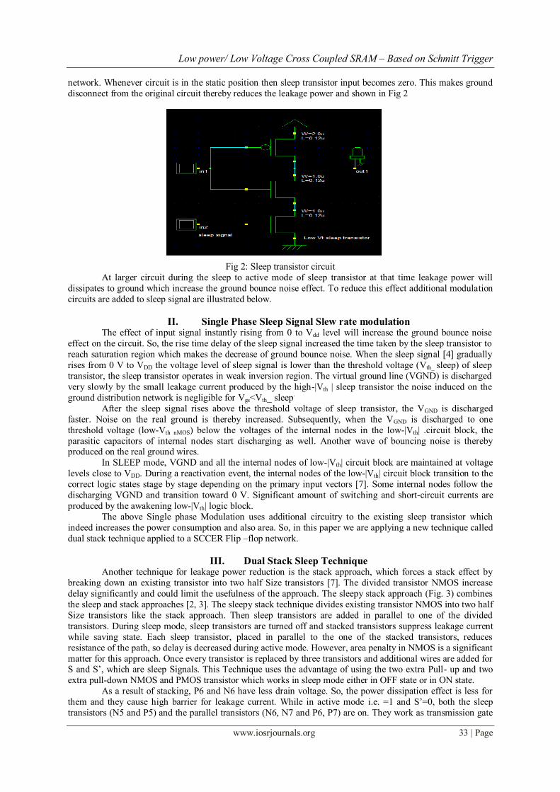
network. Whenever circuit is in the static position then sleep transistor input becomes zero. This makes ground
disconnect from the original circuit thereby reduces the leakage power and shown in Fig 2
Fig 2: Sleep transistor circuit
At larger circuit during the sleep to active mode of sleep transistor at that time leakage power will
dissipates to ground which increase the ground bounce noise effect. To reduce this effect additional modulation
circuits are added to sleep signal are illustrated below.
II. Single Phase Sleep Signal Slew rate modulation The effect of input signal instantly rising from 0 to Vdd level will increase the ground bounce noise
effect on the circuit. So, the rise time delay of the sleep signal increased the time taken by the sleep transistor to
reach saturation region which makes the decrease of ground bounce noise. When the sleep signal [4] gradually
rises from 0 V to VDD the voltage level of sleep signal is lower than the threshold voltage (Vth_ sleep) of sleep
transistor, the sleep transistor operates in weak inversion region. The virtual ground line (VGND) is discharged
very slowly by the small leakage current produced by the high-|Vth | sleep transistor the noise induced on the
ground distribution network is negligible for Vgs<Vth_ sleep.
After the sleep signal rises above the threshold voltage of sleep transistor, the VGND is discharged
faster. Noise on the real ground is thereby increased. Subsequently, when the VGND is discharged to one
threshold voltage (low-Vth nMOS) below the voltages of the internal nodes in the low-|Vth| .circuit block, the
parasitic capacitors of internal nodes start discharging as well. Another wave of bouncing noise is thereby produced on the real ground wires.
In SLEEP mode, VGND and all the internal nodes of low-|Vth| circuit block are maintained at voltage
levels close to VDD. During a reactivation event, the internal nodes of the low-|Vth| circuit block transition to the
correct logic states stage by stage depending on the primary input vectors [7]. Some internal nodes follow the
discharging VGND and transition toward 0 V. Significant amount of switching and short-circuit currents are
produced by the awakening low-|Vth| logic block.
The above Single phase Modulation uses additional circuitry to the existing sleep transistor which
indeed increases the power consumption and also area. So, in this paper we are applying a new technique called
dual stack technique applied to a SCCER Flip –flop network.
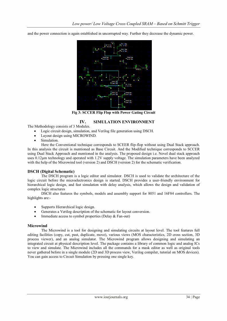
III. Dual Stack Sleep Technique Another technique for leakage power reduction is the stack approach, which forces a stack effect by
breaking down an existing transistor into two half Size transistors [7]. The divided transistor NMOS increase
delay significantly and could limit the usefulness of the approach. The sleepy stack approach (Fig. 3) combines
the sleep and stack approaches [2, 3]. The sleepy stack technique divides existing transistor NMOS into two half
Size transistors like the stack approach. Then sleep transistors are added in parallel to one of the divided
transistors. During sleep mode, sleep transistors are turned off and stacked transistors suppress leakage current
while saving state. Each sleep transistor, placed in parallel to the one of the stacked transistors, reduces
resistance of the path, so delay is decreased during active mode. However, area penalty in NMOS is a significant
matter for this approach. Once every transistor is replaced by three transistors and additional wires are added for S and S’, which are sleep Signals. This Technique uses the advantage of using the two extra Pull- up and two
extra pull-down NMOS and PMOS transistor which works in sleep mode either in OFF state or in ON state.
As a result of stacking, P6 and N6 have less drain voltage. So, the power dissipation effect is less for
them and they cause high barrier for leakage current. While in active mode i.e. =1 and S’=0, both the sleep
transistors (N5 and P5) and the parallel transistors (N6, N7 and P6, P7) are on. They work as transmission gate
Low power/ Low Voltage Cross Coupled SRAM – Based on Schmitt Trigger
www.iosrjournals.org 34 | Page
and the power connection is again established in uncorrupted way. Further they decrease the dynamic power.
Fig 3: SCCER Flip Flop with Power Gating Circuit
IV. SIMULATION ENVIRONMENT The Methodology consists of 3 Modules.
Logic circuit design, simulation, and Verilog file generation using DSCH.
Layout design using MICROWIND.
Simulation.
Here the Conventional technique corresponds to SCEER flip-flop without using Dual Stack approach.
In this analysis the circuit is mentioned as Base Circuit. And the Modified technique corresponds to SCCER
using Dual Stack Approach and mentioned in the analysis. The proposed design i.e. Novel dual stack approach
uses 0.12µm technology and operated with 1.2V supply voltage. The simulation parameters have been analyzed
with the help of the Microwind tool (version 2) and DSCH (version 2) for the schematic verification.
DSCH (Digital Schematic) The DSCH program is a logic editor and simulator. DSCH is used to validate the architecture of the
logic circuit before the microelectronics design is started. DSCH provides a user-friendly environment for
hierarchical logic design, and fast simulation with delay analysis, which allows the design and validation of
complex logic structures
DSCH also features the symbols, models and assembly support for 8051 and 16F84 controllers. The
highlights are:-
Supports Hierarchical logic design.
Generates a Verilog description of the schematic for layout conversion.
Immediate access to symbol properties (Delay & Fan-out)
Microwind The Microwind is a tool for designing and simulating circuits at layout level. The tool features full
editing facilities (copy, cut, past, duplicate, move), various views (MOS characteristics, 2D cross section, 3D
process viewer), and an analog simulator. The Microwind program allows designing and simulating an
integrated circuit at physical description level. The package contains a library of common logic and analog ICs to view and simulate. The Microwind includes all the commands for a mask editor as well as original tools
never gathered before in a single module (2D and 3D process view, Verilog compiler, tutorial on MOS devices).
You can gain access to Circuit Simulation by pressing one single key.

Low power/ Low Voltage Cross Coupled SRAM – Based on Schmitt Trigger
www.iosrjournals.org 35 | Page
Fig 4: DSCH design of SCCER Filp-Flop
Fig 5: Layout diagram
Fig 6: Simulation Wave form in Micro wind
Fig 7: DSCH design of dual stack SCCER Flip-Flop
Fig 8: Layout diagram

Low power/ Low Voltage Cross Coupled SRAM – Based on Schmitt Trigger
www.iosrjournals.org 36 | Page
Fig 9: Simulation waveforms in Micro wind
Tabulation of Results Circuit Area(um
2) Power Dissipation
SCCER 22*12 0.327mW
SCCER With dual
stack
38*14 3.297uW
V. Conclusion In nanometer scale CMOS technology, sub -threshold leakage power consumption is a great challenge.
Although previous approaches are effective in some ways, no perfect solution for reducing leakage power
consumption is yet known. Therefore, designers choose techniques based upon technology and design criteria.
In this paper, we provide novel circuit structure named “Dual stack” as a new remedy for designers in terms of
static power and dynamic powers. Unlike the sleep transistor technique, the dual stack technique retains the
original state. The dual stack approach shows the least speed power product among all methods. Therefore, the dual stack technique provides new ways to designers who require ultra-low leakage power consumption
References [1] V. Kursun and E. G. Friedman, Multi-Voltage CMOS Circuit Design, John Wiley & Sons Ltd., 2006, ISBN # 0-470-01023-1.
[2] S. Mutoh, T. Douseki, Y. Matsuya, T. Aoki, S. Shigematsu, and J. Yamada, “1-V Power Supply High-Speed Digital Circuit
Technology,” IEEE Journal of Solid-State Circuits, Vol. 30, No. 8, pp. 847-854,August 1995.
[3] J. Kao and A. Chandrakasan, “MTCMOS Sequential Circuits,” Proceedings of the European Solid State Circuits Conference, pp. 317
- 320, September 2001.
[4] S. Shigematsu, S. Mutoh, Y. Matsuya, Y. Tanabe, and J. Yamada, “A 1-V High-Speed MTCMOS Circuit Scheme for Power-Down
Application Circuits,” IEEE Journal of Solid-State Circuits, Vol. 32, No. 6. pp.861-869, June 1997.
[5] Z. Liu and V. Kursun, “New MTCMOS Flip-Flops with Simple Control Circuitry and Low Leakage Data Retention Capability,”
Proceedings of the IEEE International Conference on Electronics, Circuits, and Systems, pp. 1276-1279, December 2007.
[6] J. Kao, A. Chandrakasan, and D. Antoniadis, “Transistor Sizing Issues and Tool for Multi-Threshold CMOS Technology,”
Proceedings of the IEEE/ACM International Design Automation Conference, pp. 409 - 414, June 1997. [7] B. H. Calhoun, F. A. Honore, and A. P. Chandrakasan, “A Leakage Reduction Methodology for Distributed MTCMOS,” IEEE
Journal of Solid-State Circuits, Vol. 39, No. 2, pp. 818 - 826, May 2004.
[8] S. A. Tawfik and V. Kursun, “Low-Power and Compact Sequential Circuits with Independent-Gate Fin FETs,” IEEE Transactions on
Electron Devices,
Vol. 55, Number 1, pp. 60-70, January 2008.
[9] R. Kumar and G. Hinton, “A Family of 45nm IA Processors,” Proceedings of the IEEE International Solid-State Circuits Conference,
pp. 58-59, February2009.
[10] Z. Liu and V. Kursun, “High Read Stability and Low Leakage SRAM Cell Based on Data/Bitline Decoupling,” Proceedings of the
IEEE International Systems on Chip (SOC) Conference, pp. 115-116, September 2006.
[11] R. S. Muller, T. I. Kamins, and M. Chan, Device Electronics for Integrated Circuits, John Wiley &Sons Ltd., 2002, ISBN #
0471593982.
[12] http://www.umc.com/english/process/g.asp. UMC 90 Nanometer CMOS Technology.
Tarunnum Sultana1 Assistant professor in Electronic and Communication engineering in SSJ
College of Engineering. She received her B.Tech Degree in Electronics & Communication
Engineering from Gurunanak Dev Engineering College from Bidar, Karnataka and M.Tech
Degree in DSCE from Shadan women’s Engineering College Hyderabad and her current
interest in Digital Electronics.

Low power/ Low Voltage Cross Coupled SRAM – Based on Schmitt Trigger
www.iosrjournals.org 37 | Page
S. Jagadeesh2, Associate Professor and HOD in SSJ Engineering College, Hyderabad. He
received his B. Tech Degree in Electronics & Communication Engineering from SKDU, Ananthapur and M. Tech Degree in Electronics and Communication Engineering from
JNTUH, Hyderabad. He was a Research scholar in Electronics & communication Engineering
Department, JNTUH. He has more than 13 years of experience in teaching and research. His
current interest includes Digital image processing and electronics.
M. Naveen Kumar3, M.Tech-VLSI Student of SSJ Engineering College, JNTUH, Hyderabad. He
is completed his B. Tech in Electronics and Communication Engineering from DRK
Engineering college, JNTUH, Hyderabad.