A Novel Complete High Precision Standard Linear …A Novel Complete High Precision Standard Linear...
15
A Novel Complete High Precision Standard Linear Element-Based Equivalent Circuit Model of CMOS Gyrator-C Active Transformer RAWID BANCHUIN Department of Computer Engineering Siam University 235 Petchakasem Rd., Phasi-charoen, Bangkok 10163 THAILAND rawid_b@yahoo.com Abstract: - In this research, the novel equivalent circuit model of the CMOS gyrator-C active transformer has been proposed. Besides the effect of the unwanted intrinsic elements, the effect of the finite open loop bandwidth, which was neglected in previous research, is also taken into account. By this reason, it is a complete model. The proposed model is constructed based upon the simple standard linear elements and can accurately simulate the characteristics of the CMOS gyrator-C active transformer for various decades of frequency which cover the operating range of the on-chip monolithic transformer given by a few GHz up to 10 GHz. The percentage of deviations between each of the parameters obtained from the equivalent circuit model and a similar one obtained from the original active transformer were found to be very small, for example, the deviation between the Re[z 11 ], Im[z 11 ] and Re[z 21 ] of the model and the topology II active transformer have been found to be lower than 0.007%, 0.2703% and 0.0139% respectively. The average computational times for the simulations are significantly reduced by using this model. Hence, the proposed model has been found to be a convenient tool for both manual and computer based analysis/design of various applications involving the CMOS gyrator-C active transformer. Furthermore, a simple procedure to minimize the effects of both major nonidealities is also discussed. Key-Words: - On-chip monolithic transformer, CMOS gyrator-C active transformer, Equivalent circuit model, Standard linear element, High order element 1 Introduction The on-chip monolithic transformer has been adopted in many analog/mixed signal applications nowadays, for example, Low Noise Amplifiers (LNA), mixers, and oscillators. These applications have been employed in many areas such as telecommunications, measurement and instrumentation. Originally, the passive onchip monolithic transformer was constructed based on a spiral inductor with no active elements included as proposed in many researches for example, [1]-[6]. However, the drawbacks of a spiral inductor such as the large chip area and lack of tuning capability, are inherited by the cited passive on-chip transformer. Later, the Distributed Active Transformer (DAT) which is constructed by using both passive and active elements, inductive metals and transistors, respectively, was proposed in many researches for example, [7]-[10]. However, to the knowledge of the author, there is no application of DAT other than power combining and impedance transformation. Finally, an active on-chip monolithic transformer with no inductive metal include, has been proposed by F. Yuan [11]. This active transformer, CMOS gyrator-C active transformer [11], was constructed based upon the CMOS technology by using the active coupling of the gyrator-C based active inductors via the transconductors. According to [12], the CMOS gyrator-C active transformer has many far superior characteristics compared with the passive ones, for example, tunability of the coupling ratio, larger and tunable self and mutual inductances, higher and tunable quality factors, and a smaller chip area. This CMOS gyrator-C active transformer has been adopted in various analog/mixed signal applications such as quadrature oscillators [12], voltage controlled oscillators [13], current-mode phase-lock loops [14] and QPSK modulators [15] which are obviously employed in many areas in circuits and systems engineering. Hence, it has been found to be the most interesting on-chip monolithic transformer. For convenience in the analysis and design of any analog/mixed signal application, a simple and precise model of any complicated element with significant intrinsic nonidealities such as a transconductor, an OP-AMP, or on-chip monolithic transformer, is necessary. By using the model, both WSEAS TRANSACTIONS on CIRCUITS and SYSTEMS Rawid Banchuin E-ISSN: 2224-266X 67 Issue 3, Volume 11, March 2012
Transcript of A Novel Complete High Precision Standard Linear …A Novel Complete High Precision Standard Linear...
A Novel Complete High Precision Standard Linear Element-Based Equivalent Circuit Model of CMOS Gyrator-C Active Transformer
RAWID BANCHUIN
Department of Computer Engineering Siam University
235 Petchakasem Rd., Phasi-charoen, Bangkok 10163 THAILAND
[email protected] Abstract: - In this research, the novel equivalent circuit model of the CMOS gyrator-C active transformer has been proposed. Besides the effect of the unwanted intrinsic elements, the effect of the finite open loop bandwidth, which was neglected in previous research, is also taken into account. By this reason, it is a complete model. The proposed model is constructed based upon the simple standard linear elements and can accurately simulate the characteristics of the CMOS gyrator-C active transformer for various decades of frequency which cover the operating range of the on-chip monolithic transformer given by a few GHz up to 10 GHz. The percentage of deviations between each of the parameters obtained from the equivalent circuit model and a similar one obtained from the original active transformer were found to be very small, for example, the deviation between the Re[z11], Im[z11] and Re[z21] of the model and the topology II active transformer have been found to be lower than 0.007%, 0.2703% and 0.0139% respectively. The average computational times for the simulations are significantly reduced by using this model. Hence, the proposed model has been found to be a convenient tool for both manual and computer based analysis/design of various applications involving the CMOS gyrator-C active transformer. Furthermore, a simple procedure to minimize the effects of both major nonidealities is also discussed. Key-Words: - On-chip monolithic transformer, CMOS gyrator-C active transformer, Equivalent circuit model, Standard linear element, High order element 1 Introduction The on-chip monolithic transformer has been adopted in many analog/mixed signal applications nowadays, for example, Low Noise Amplifiers (LNA), mixers, and oscillators. These applications have been employed in many areas such as telecommunications, measurement and instrumentation. Originally, the passive onchip monolithic transformer was constructed based on a spiral inductor with no active elements included as proposed in many researches for example, [1]-[6]. However, the drawbacks of a spiral inductor such as the large chip area and lack of tuning capability, are inherited by the cited passive on-chip transformer. Later, the Distributed Active Transformer (DAT) which is constructed by using both passive and active elements, inductive metals and transistors, respectively, was proposed in many researches for example, [7]-[10]. However, to the knowledge of the author, there is no application of DAT other than power combining and impedance transformation.
Finally, an active on-chip monolithic transformer with no inductive metal include, has been proposed by F. Yuan [11]. This active transformer, CMOS
gyrator-C active transformer [11], was constructed based upon the CMOS technology by using the active coupling of the gyrator-C based active inductors via the transconductors. According to [12], the CMOS gyrator-C active transformer has many far superior characteristics compared with the passive ones, for example, tunability of the coupling ratio, larger and tunable self and mutual inductances, higher and tunable quality factors, and a smaller chip area. This CMOS gyrator-C active transformer has been adopted in various analog/mixed signal applications such as quadrature oscillators [12], voltage controlled oscillators [13], current-mode phase-lock loops [14] and QPSK modulators [15] which are obviously employed in many areas in circuits and systems engineering. Hence, it has been found to be the most interesting on-chip monolithic transformer.
For convenience in the analysis and design of any analog/mixed signal application, a simple and precise model of any complicated element with significant intrinsic nonidealities such as a transconductor, an OP-AMP, or on-chip monolithic transformer, is necessary. By using the model, both
WSEAS TRANSACTIONS on CIRCUITS and SYSTEMS Rawid Banchuin
E-ISSN: 2224-266X 67 Issue 3, Volume 11, March 2012
manual and automated analysis/design effort can be significantly reduced while the acceptable analysis/design precision can be maintained. For example, by using the model proposed in [16] to simulate the behavior of the digital to analog converter, the computational time can be significantly reduced by a factor of 874 compared to that required for the simulation of the original digital to analog converter circuit where as the simulation error of below 1% can be achieved [16]. This computational time reduction is obviously an important issue in the analysis/design of analog/mixed signal applications nowadays which the transistor level simulation of the entire system is infeasible in the computational time aspect since the nanometer CMOS technology allows the integration of a tremendous number of transistors into a single system on chip [17]. Furthermore, the analysis and designing of any application by using the model can be performed in a much simpler fashion than those using the original transistor level circuit.
For the on-chip monolithic active transformer of our interest, its equivalent circuit models have been proposed in [11], [13] and. Obviously, the effects of both major nonidealities of the basis transconductor entitled unwanted intrinsic elements and finite open loop bandwidth must be taken into account for the model to be complete similarly to the models of the OTA-based inductors proposed in [18]. However the models proposed in [11] and [13] take only the effect of the unwanted intrinsic elements into account while the finite open loop bandwidth has been totally ignored. So, they are incomplete. Later, an improved model has been proposed in [19]. The effects of both nonidealities mentioned above have been taken into account. As such, it is a complete model. However, this model contains a super inductor which is a troublesome high order element as discussed in [18, 19] and will be seen later. So, this model is considered to be a complicate one which seriously requires modification.
Hence, the novel equivalent circuit model of the CMOS gyrator-C active transformer is proposed in this research. The effects of both nonidealities have been taken into account. So, it is also a complete model. Furthermore, the proposed model has been found to be very convenient since it has been constructed based upon the ordinary R and L which can be classified as the simple standard linear elements along with the ideal linearly controlled voltage/current sources only. There is none of any complicate high order element included. The characteristics of the CMOS gyrator-C active transformer can be accurately simulated by the proposed model for various decades of the operating
frequency which cover the operating range of the on chip monolithic transformer given by a few GHz up to 10 GHz [20-22]. With the acceptable accuracies, the average computational times of the simulations using the proposed models are significantly reduced compared to those for the original active transformer circuits based simulations. Therefore, it has been found to be an efficient tool for both manual/automated analysis and design of various applications involving the CMOS gyrator-C active transformer. Furthermore, a simple procedure to minimize the effects of both major nonidealities has also been suggested in this study.
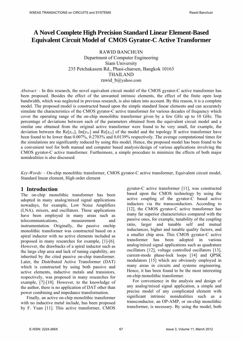
2 An Overview of CMOS Gyrator-C Active Transformer In this section, an overview of the CMOS gyrator-C active transformer will be discussed. The gyrator-C active transformer can be constructed by the active coupling of the gyrator-C active inductor via the transconductors. They can be classified into two topologies entitled topology I and topology II according to [11], which can be depicted in fig.1 and fig.2 respectively.
It should be mentioned here that gmi where {i} = {1, 2} and gij where {i} = {1, 2} and {j} = {1, 2}, denote the transconductances of the transconductors within the basis active inductors and those of the coupling transconductors, respectively.
According to [11-15], each transconductor within the active transformer has been simply realized by a single MOS transistor of either n or p-type. So, the resulting active transformer can be entitled CMOS gyrator-C active transformer. Both topologies of the resulting CMOS gyrator-C active transformers have been realized as proposed in [11] which can be depicted in fig. 3 where each basis transconductor has been simply realized by a single MOS transistor. Fig. 1 Topology I gyrator-C active transformer
WSEAS TRANSACTIONS on CIRCUITS and SYSTEMS Rawid Banchuin
E-ISSN: 2224-266X 68 Issue 3, Volume 11, March 2012

Fig. 2 Topology II gyrator-C active transformer
Fig. 3 Realization of CMOS-gyrator-C active transformer: Topology I (above) and Topology II (below). 3 The Proposed Equivalent Circuit Model The proposed equivalent circuit model will be presented in this section. The effects of both unwanted intrinsic elements and finite open loop bandwidth have been taken into account. Since, a MOS transistor is adopted as the basis transconductor, the unwanted intrinsic elements are gds and Cgd. This is because Cgs is ideally untilized as the capacitive part for the CMOS gyrator-C active inductors which serve as the primary and secondary windings of the active transformer. In this study, the finite open loop bandwidth means the finite transition frequency, fT of the MOS transistor.
At this point, it should be mentioned here that all transistors within the active transformer are assumed to be identical. This assumption, which has also been adopted in [19], is acceptable since the
mismatch among the MOS transistors within the same monolithic IC has been found to be very small according to [23, 24]. Hence, fT along with gds, Cgd and Cgs of each basic MOS transistor are assumed to be identical.
Note also that the single pole model of the frequency dependent transconductance, gm(s) [25] is employed in order to demonstrate the effect of fT. This single pole model which demonstrates the effect of the finite open loop bandwidth of the OTA and also adopted in [18] is adequate to demonstrate the effect of fT since a MOS transistor is basically a transconductor like an OTA as also mentioned in [19]. Hence, gm(s) can be defined in this research as follows
τsgsg m
m +=
1)( 0 (1)
where gm0 denotes the dc-transconductance of
any basis MOS transistor. It should be mentioned here that τ which denotes the time delay [25] can be given as a function of fT by
Tfπτ
21
= (2)
Even though fT, gds, Cgd and Cgs have been
assumed to be identical, this assumption is not applied to gm0. This is for the resulting model being capable to reflect the tuning capability of the active transformer which is the result of the independent tuning capability of gm0 of each basis MOS transistor. Hence, gm0 of the MOS transistors within the active based primary/secondary windings are denoted by gm01 and gm02 where as those of active coupling transistors are given by gm012 and gm021 respectively.
By taking both major nonidealities into account, both self and mutual impedances of the CMOS gyrator-C active transformer are not purely inductive anymore. These impedances can be commonly given by
ijijijij sssZ γβα ++= 2)( (3)
where {i} = {1, 2} and {j} = {1, 2}. In other words, the coefficients for both self impedances which are Z11(s) and Z22(s) can be denoted by α11, β11 and γ11 for Z11(s) along with α22, β22 and γ22 for Z22(s). On the other hand, the coefficients for both mutual impedances which are Z12(s) and Z21(s) can be denoted by α12, β12 and γ12 for Z12(s) along with
WSEAS TRANSACTIONS on CIRCUITS and SYSTEMS Rawid Banchuin
E-ISSN: 2224-266X 69 Issue 3, Volume 11, March 2012
α21, β21 and γ21 for Z21(s). For the topology I active transformer, these coefficients can be given by
dsmmmmm
gdmgsdsm
ggggggCgCgg
)()(2
021012020101
010211 −
+=
τα (4)
dsmmmmm
dsgdmgsdsm
gggggggCgCgg)(
)4(
021012020101
20102
11 −++
=τ
β (5)
dsmmmmm
dsm
gggggggg
)(2
021012020101
202
11 −=γ (6)
dsmmmmm
gdmgsdsm
ggggggCgCgg
)()(2
021012020102
020122 −
+=
τα (7)
dsmmmmm
dsgdmgsdsm
gggggggCgCgg)(
)4(
021012020102
20201
22 −++
=τ
β (8)
dsmmmmm
dsm
gggggggg
)(2
021012020102
201
22 −=γ (9)
dsmmmmm
gdgsdsm
ggggggCCgg
)()(2
021012020102
0212 −
+=
τα (10)
dsmmmmm
dsgdmgsdsm
gggggggCgCgg)(
)4(
021012020102
202012
12 −++
=τ
β (11)
dsmmmmm
dsm
gggggggg
)(2
021012020102
2012
12 −=γ (12)
dsmmmmm
gdmgsdsm
ggggggCgCgg
)()(2
021012020101
0102121 −
+=
τα (13)
dsmmmmm
dsgdmgsdsm
gggggggCgCgg)(
)4(
021012020101
202021
21 −++
=τ
β (14)
and
dsmmmmm
dsm
gggggggg
)(2
021012020101
2021
21 −=γ (15)
On the other hand, for the active transformer of
topology II, these coefficients can be given by
dsmmmmm
gdmgdmgsdsm
ggggggCgCgCgg
)(])[(2
021012020101
021010211 −
++=
τα (16)
dsmmmmm
gdmdsgdmgsdsm
ggggggCggCgCgg
)(])2[(
021012020101
0212
010211 −
+++=
τβ (17)
dsmmmmm
dsm
gggggggg
)( 021012020101
202
11 −=γ (18)
dsmmmmm
gdmmgsdsm
ggggggCggCgg)(
])([2
021012020102
012020122 −
++=
τα (19)
dsmmmmm
dsgdmmgsdsm
gggggggCggCgg
)(]2)([
021012020102
20120201
22 −+++
=τ
β (20)
dsmmmmm
dsm
gggggggg
)( 021012020102
201
22 −=γ (21)
dsmmmmm
gdmmgsdsm
ggggggCggCgg)(
])([2
021012020101
0210101212 −
++=
τα (22)
dsmmmmm
dsgdmmgsdsm
gggggggCggCgg
)(]2)([
021012020101
202101012
12 −+++
=τ
β (23)
dsmmmmm
dsm
gggggggg
)( 021012020101
2012
12 −=γ (24)
dsmmmmm
gdmmgsdsm
ggggggCggCgg
)(])([2
021012020101
0120202121 −
++=
τα (25)
dsmmmmm
dsgdmmgsdsm
gggggggCggCgg
)(]2)([
021012020101
201202021
21 −+++
=τ
β (26)
and
dsmmmmm
dsm
gggggggg
)( 021012020102
2021
21 −=γ (27)
Based on the concept of using the ideal
controlled sources to realize the mutual coupling of the transformer which is adopted in [21] and [26], the prototype model for both topologies of the active transformer can be depicted as in fig.4.
It can be seen from fig.4 that each Zij(s) can be realized as a series combination of the super inductor (Ls) of the size αij, the ordinary L of the size βij and the ordinary R of the size γij. For both topologies, the analytical expressions of the size of these elements for any Zij(s) can be found from (4)-(27). This Ls based equivalent circuit model has been proposed in [19]. However, as proposed in [18, 19], the constitutive relation of Ls ( ),( φif
SL ) can be given by
),( φifSL : ∫=
t
S
dL
i0
)(1 ττφ (28)
where i and ø denote the current and magnetic
flux respectively. They are both physically meaningful variables. Since this constitutive relation is not a strictly linear algebraic function of i and ø because it contains the integration, Ls cannot be
WSEAS TRANSACTIONS on CIRCUITS and SYSTEMS Rawid Banchuin
E-ISSN: 2224-266X 70 Issue 3, Volume 11, March 2012
classified as a standard linear element. This is because the constitutive relations of any standard linear element must be a strictly linear algebraic function of their corresponding physically meaningful variables only [18, 19]. Hence, as also proposed in [18], there can be only three elements which can be classified as standard linear ones. These elements are the ordinary R, L and C respectively since their constitutive relations have been found to be strictly linear algebraic function of their corresponding physically meaningful variables as mentioned in [18].
Furthermore, the impedance function of Ls is given by [18, 19]
SLssZ 2)( = (29)
From this impedance function, Ls can be
classified as a high order element since the order of s is larger than 1 [18, 19]. As a high order element, Ls is far complicate to R, L and C. It has been found to be an inferior building block for the modeling purposes compared to those standard linear elements as proposed in [18, 19]. Hence, this prototype Ls based model requires much improvement in order to avoid the troublesome Ls while maintaining the accuracy as stated in [19].
By the similar mathematical methodology to that used in [18], each Zij(s) can be similarly approximated by
ijijij RsLsZ +=)( (30)
where (31) and
(32)
Hence, each Zij(s) can be now realized as a series combination of the ordinary L of the size Lij and the ordinary R of the size Rij. As mentioned earlier, both ordinary R and L are the standard linear element since their constitutive relations ( ),( vif R and ),( φif L ) can be given respectively by
),( vif R : v = iR (33)
and
),( φif L : ø= Li (34) Obviously, these constitutive relations are
strictly linear functions of voltage (v), i and ø which are physically meaningful. Based upon this realization of Zij(s) by the standard linear elements which are ordinary R and L in this srudy, the proposed standard linear element based equivalent circuit model for both topologies of CMOS-gyrator-C active transformer can be constructed as shown in fig.5.
By using (4)-(15) along with (31) and (32), the analytical expressions of the elements of the model for topology I active transformer can be given by
dsmmmmm
dsgsdsgdmm
gggggggCgCgg
L)(
)]4([
021012020101
010211 −
−+=
τ (35)
))(()]4([2
01021012020101
010211
gsdsgdmmmmmm
dsdsgsdsgdmm
CgCggggggggCgCgg
R+−
−+=
τ (36)
dsmmmmm
dsgsdsgdmm
gggggggCgCgg
L)(
)]4([
021012020101
020122 −
++=
τ (37)
))(()]4([
02021012020102
020122
gsdsgdmmmmmm
dsdsgsdsgdmm
CgCggggggggCgCgg
R+−
++=
τ(38)
dsmmmmm
gsdsgdmm
ggggggCgCgg
M)()(
021012020102
0201212 −
+= (39)
(40)
dsmmmmm
dsgsdsgdmm
gggggggCgCgg
M)(
)]4([
021012020101
0102121 −
−+=
τ (41)
and
))(()]4([2
01021012020101
0102121
gsdsgdmmmmmm
dsdsgsdsgdmm
CgCggggggggCgCgg
R+−
−+=
τ (42)
On the other hand these expressions can be
alternatively given for topology II by using (16)-(27), (31) and (32) as follows:
ijijijijL γαβ 42 −=
]}4[4{)2( 21ijijijijijijijijijR γαββββαα −−−= −
))((]4
)4()4[(
02101202012
02
2012
0201201202012
12gsdsgdmmmmm
dsdsm
gdmmgsdsmmm
CgCgggggggg
CggCgggg
R+−
−
−+−
=τ
WSEAS TRANSACTIONS on CIRCUITS and SYSTEMS Rawid Banchuin
E-ISSN: 2224-266X 71 Issue 3, Volume 11, March 2012

dsmmmmm
dsgsdsgdmmm
gggggggCgCggg
L)(
)]2()[(
021012020101
021010211 −
−++=
τ (43)
])[()(
)]2(
)[(
02101
021012020101
0210102
11
gsdsgdmm
mmmmm
dsdsgsds
gdmmm
CgCgggggggggCg
Cggg
R
++−
−+
+
=τ
(44)
dsmmmmm
dsgsdsgdmmm
gggggggCgCggg
L)(
)]2()[(
021012020102
012010122 −
−++=
τ (45)
τ
τ
dsgsdsgdm
mmmmm
dsgsdsgdmm
gdgsdsgdmmmm
gCgCg
ggggggCgCgg
CCgCgggg
R
)2(
)(4])2)3((2
)2)([(
02
021012020102
202012
020201201
22
+×
−
+++
+−
= (46)
dsmmmmm
dsgsdsgdmmm
gggggggCgCggg
M)(
)]2()[(
021012020101
0210101212 −
−++=
τ (47)
])[()(
)]2(
)[(
02101
021012020101
02101012
12
gsdsgdmm
mmmmm
dsdsgsds
gdmmm
CgCggggggg
ggCg
Cggg
R
++×−
−+
+
=τ (48)
dsmmmmm
dsgsdsgdmmm
gggggggCgCggg
M)(
)]2()[(
021012020102
0120202121 −
−++=
τ (49)
and
])[()(
)]2()[(
01202
021012020102
0120202121
gsdsgdmm
mmmmm
dsdsgsdsgdmmm
CgCggggggg
ggCgCgggR
++×−
−++=
τ (50)
So, it can be seen from (35)-(50) that the effect
of the finite open loop bandwidth is captured by the proposed model due to the inclusion of τ which is the function of fT. It can also be seen from these equations that the effect of unwanted intrinsic elements is also captured due to the inclusion of gds and Cgd. Hence, the proposed standard linear element based equivalent circuit model has been found to be complete since the effects of both major nonidealities of the basis transconductor have been included.
4 The Model Verification The accuracy verification of the proposed model will be performed in this section. In order to do so, the comparisons between the frequency responses of Re[Z11(ω)], ω-1Im[Z11(ω)], Re[Z21(ω)], ω-
1Im[Z21(ω)] and voltage transfer ratio (n), obtained from the model and the original active transformer have been performed for both topologies. Mathematically, n can be defined as follows
(51)
where V1 and V2 denote the voltages at the
primary and secondary terminal respectively. The chosen frequency range is given by 0.1 kHz
up to 10 GHz which cover the operating range of the on chip monolithic transformer according to [20-22]. The realization of the original active transformers has been performed based upon the 90 nm CMOS technology due to the rise of the nanometer CMOS technology. For the model parameterizations, the values of gds, Cgd, Cgs and fT at 90 nm level have been used where as those electronically tunable dc transconductances can be given for both topologies in Table 1
In order to verify the accuracy of the proposed model quantitatively, the percentage of deviation in the parameter of interest has been used. Let the parameter of interested be x which can be either Re[Z11(ω)], ω-1Im[Z11(ω)], Re[Z21(ω)], ω-
1Im[Z21(ω)] or n, this percentage of deviation can be defined as follows:
(52)
where xmodel denotes any parameter of interest
obtained from the model and xoriginal denotes the similar parameter of the original active transformer respectively. Hence, there are five deviations of interested for each topology which are δRe[Z11(ω)], δω-
1Im[Z11(ω)], δRe[Z21(ω)], δω-1Im[Z21(ω)] and δn. At this point, the comparative frequency
responses of Re[Z11(ω)], ω-1Im[Z11(ω)], Re[Z21(ω)], ω-1Im[Z21(ω)] and n obtained from the original active transformer of topology I (Fig. 2) and the proposed model can be respectively plotted in Fig.(6)-(10). On the other hand, the similar comparative frequency responses between the original active transformer of topology II (Fig. 3) and the model can be plotted in Fig.(11)-(15).
For both topologies, the frequency responses of Re[Z11(ω)], ω-1Im[Z11(ω)], Re[Z21(ω)], ω-
1Im[Z21(ω)] and n obtained from the proposed
1
2
VV
n =
%100model ×−
=original
originalx x
xxδ
WSEAS TRANSACTIONS on CIRCUITS and SYSTEMS Rawid Banchuin
E-ISSN: 2224-266X 72 Issue 3, Volume 11, March 2012

model keep accurately tracking their counterparts obtained from the original active transformer along the chosen frequency range. This can be quantitatively stated that δRe[Z11(ω)], δω-1Im[Z11(ω)], δRe[Z21(ω)], δω-1Im[Z21(ω)] and δn which given in Table 2, have been found to be very small. So, the proposed model has been verified in both qualitative and quantitative aspects to be highly accurate and applicable for the entire typical operating range of the on-chip transformer according to the chosen frequency range.
Furthermore, the average computational times obtained from 100 simulations for each topology have also been recorded as shown in Table 3. It can be seen that significant reductions between the average computational times obtained from the model based simulations and those from the original active transformers based simulations can be observed. In the quantitative aspect, the factor of computational time reduction can be mathematically given by
modeltt
F originalR = (53)
where tmodel denotes the average computational
time obtained from the model based simulations and toriginal denotes obtained from the simulations of the original active transformer respectively.
According to the satisfied verification results the proposed model has been found to be a convenient tool for the analysis and design of various applications involving the CMOS gyrator-C active transformer. The model is applicable in various fields of analog/mixed signal circuits and system engineering. Table 1. DC transconductances of the basis MOS transistor
Topology I Topology II
gm01 412.655 mS 412.655 mS
gm02 41.2655 mS 41.2655 mS
gm012 130.487 mS 13.0487 mS
gm021 130.487 mS 13.0487 mS
Table 2. δRe[Z11(ω)], δω-1Im[Z11(ω)], δRe[Z21(ω)], δω-1Im[Z21(ω)] and δn
Topology I Topology II
δRe[Z11(ω)] ≤ 1.72% ≤ 0.007%, δω-Im[Z11(ω)] ≤ 1.59% ≤ 0.2703%
δRe[Z21(ω)] ≤ 2.04% ≤ 0.0139%
δω-Im[Z21(ω)] ≤ 1.69% ≤ 0.34%
δn ≤ 4% ≤ 3.09%
Table 3. Average computational times and the reductions for both topologies
Topology I Topology II
tmodel (ms)
toriginal (ms) FR
tmodel (ms)
toriginal (ms) FR
21
5466
260.3
20 5212
260.6
5 Discussion The procedure to minimize the effects of both major nonidealities will be discussed in this section. In the ideal situation, the effects of these major nonidealities are not taken into account. So, both self and mutual impedances of the CMOS gyrator-C active transformer are purely inductive. This means that R11 = R22 = R12 = R21 = 0 for both topologies. Furthermore, the magnitudes of deviation from the desired values of both self and mutual inductances are not existed for both topologies. Regardless to the topology, these magnitudes of deviation can be defined for self and mutual inductances respectively as follows
111111 LLL d −=Δ (54)
222222 LLL d −=Δ (55)
121212 MMM d −=Δ (56)
212121 MMM d −=Δ (57)
WSEAS TRANSACTIONS on CIRCUITS and SYSTEMS Rawid Banchuin
E-ISSN: 2224-266X 73 Issue 3, Volume 11, March 2012

Fig. 4. The prototype equivalent circuit model of CMOS-gyrator-C active transformer.
Fig. 5. The proposed standard linear element based equivalent circuit model of CMOS-gyrator-C active transformer.
WSEAS TRANSACTIONS on CIRCUITS and SYSTEMS Rawid Banchuin
E-ISSN: 2224-266X 74 Issue 3, Volume 11, March 2012
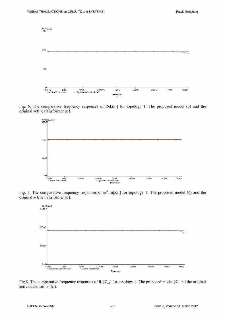
Fig. 6. The comparative frequency responses of Re[Z11] for topology 1: The proposed model (◊) and the original active transformer (□).
Fig. 7. The comparative frequency responses of ω-1Im[Z11] for topology 1: The proposed model (◊) and the original active transformer (□).
Fig.8. The comparative frequency responses of Re[Z21] for topology 1: The proposed model (◊) and the original active transformer (□).
WSEAS TRANSACTIONS on CIRCUITS and SYSTEMS Rawid Banchuin
E-ISSN: 2224-266X 75 Issue 3, Volume 11, March 2012

Fig. 9. The comparative frequency responses of ω-1Im[Z21] for topology 1: The proposed model (◊) and the original active transformer (□).
Fig. 10. The comparative frequency responses of n for topology 1: The proposed model (◊) and the original active transformer (□).
Fig. 11. The comparative frequency responses of Re[Z11] for topology 2: The proposed model (◊) and the original active transformer(□).
WSEAS TRANSACTIONS on CIRCUITS and SYSTEMS Rawid Banchuin
E-ISSN: 2224-266X 76 Issue 3, Volume 11, March 2012

.
Fig. 12. The comparative frequency responses of ω-1Im[Z11] for topology 2: The proposed model (◊) and the original active transformer(□).
Fig.13. The comparative frequency responses of Re[Z21] for topology 2: The proposed model (◊) and the original active transformer(□).
Fig. 14. The comparative frequency responses of ω-1Im[Z21] for topology 2: The proposed model (◊) and the original active transformer(□).
WSEAS TRANSACTIONS on CIRCUITS and SYSTEMS Rawid Banchuin
E-ISSN: 2224-266X 77 Issue 3, Volume 11, March 2012
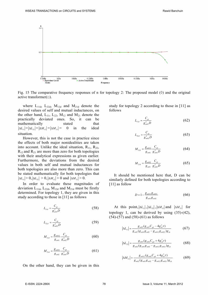
Fig. 15 The comparative frequency responses of n for topology 2: The proposed model (◊) and the original active transformer(□).
where L11d, L22d, M12d and M21d denote the desired values of self and mutual inductances, on the other hand, L11, L22, M12 and M21 denote the practically deviated ones. So, it can be mathematically stated that
11LΔ = 22LΔ = 12MΔ = 21MΔ = 0 in the ideal situation.
However, this is not the case in practice since the effects of both major nonidealities are taken into account. Unlike the ideal situation, R11, R22, R12 and R21 are more than zero for both topologies with their analytical expressions as given earlier. Furthermore, the deviations from the desired values in both self and mutual inductances for both topologies are also more than zero. This can be stated mathematically for both topologies that
11LΔ > 0, 22LΔ > 0, 12MΔ > 0 and 21MΔ > 0. In order to evaluate these magnitudes of
deviation L11d, L22d, M12d and M21d must be firstly determined. For topology 1, they are given in this study according to those in [11] as follows
DgC
Lm
gsd 2
0111 = (58)
DgC
Lm
gsd 2
0222 = (59)
DgC
gg
Mm
gs
m
md 2
0201
01212 = (60)
DgC
gg
Mm
gs
m
md 2
0102
02121 = (61)
On the other hand, they can be given in this
study for topology 2 according to those in [11] as follows
DgC
Lm
gsd 2
0111 = (62)
DgC
Lm
gsd 2
0222 = (63)
DgC
gg
Mm
gs
m
md 2
0102
01212 = (64)
DgC
gg
Mm
gs
m
md 2
0201
02121 = (65)
It should be mentioned here that, D can be
similarly defined for both topologies according to [11] as follow
0201
0210121mm
mm
gggg
D −= (66)
At this point, 11LΔ , 22LΔ , 12MΔ and 21MΔ for
topology 1, can be derived by using (35)-(42), (54)-(57) and (58)-(61) as follows
dsmmmmm
dsgdmm
gggggggCgg
L)(
)4(
021012020101
20102
11 −
−=Δ
τ (67)
dsmmmmm
dsgdmm
gggggggCgg
L)(
)4(
021012020102
20201
22 −
+=Δ
τ (68)
dsmmmmm
dsgdmm
gggggggCgg
M)()4(
021012020102
202012
12 −
+=Δ
τ (69)
WSEAS TRANSACTIONS on CIRCUITS and SYSTEMS Rawid Banchuin
E-ISSN: 2224-266X 78 Issue 3, Volume 11, March 2012

dsmmmmm
dsgdmm
gggggggCgg
M)()4(
021012020101
201021
21 −
−=Δ
τ (70)
where as those for topology 2 can be found by
using (43)-(50), (54)-(57) and (62)-(65) as follows
dsmmmmm
dsgdmmm
gggggggCggg
L)(
]2)[(
021012020101
20210102
11 −
−+=Δ
τ (71)
dsmmmmm
dsgdmmm
gggggggCggg
L)(
]2)[(
021012020102
20120201
22 −
−+=Δ
τ (72)
dsmmmmm
dsgdmmm
gggggggCggg
M)(
]2)[(
021012020101
202101012
12 −
−+=Δ
τ (73)
dsmmmmm
dsgdmmm
gggggggCggg
M)(
]2)[(
021012020102
202012021
21 −
−+=Δ
τ (74)
From these magnitudes of deviation, it can be
concluded for both topologies that
021012020111
1
mmmm ggggL
−∝Δ (75)
021012020122
1
mmmm ggggL
−∝Δ (76)
021012020112
1
mmmm ggggM
−∝Δ (77)
021012020121
1
mmmm ggggM
−∝Δ (78)
Furthermore, it can also be concluded for both
topologies from the observation of (36), (38), (40), (42), (44), (46), (48) and (50) that
021012020111
1
mmmm ggggR
−∝ (79)
021012020122
1
mmmm ggggR
−∝ (80)
021012020112
1
mmmm ggggR
−∝ (81)
021012020121
1
mmmm ggggR
−∝ (82)
Obviously, these unwanted magnitudes of
deviation and resistances which are the effects
both major nonidealities can be vastly reduced if
0210120201 mmmm gggg >> (83)
Hence, it has been found that the procedure to minimize the effects of both major nonidealities is to let gm01 and gm02 which are the dc transconductances of the transistors within the active based primary/secondary windings, be much larger than gm012 and gm021 which are the dc transconductances the active coupling transistors. This can be easily accomplished since these dc transconductances are electronically controllable. 6 Conclusion In this research, the novel standard linear element based equivalent circuit model of the CMOS gyrator-C active transformer has been proposed. The proposed model has been found to be complete since the effects of both unwanted intrinsic elements and finite open loop bandwidth are included. The proposed model has been found to be very simple since it is composed only of the standard linear elements. It can simulate the characteristics of the target active transformer with high accuracy for various decades of frequency from 0.1 kHz up to 10 GHz which cover the typical operating range of the on chip monolithic transformer. Furthermore, the average computational times of the simulations can be significantly reduced by using the proposed models. Finally, the procedure to minimize the effects of both major nonidealities has been discussed.
Hence, the proposed model has been found to be a convenient tool for the analysis and design of various applications involving the CMOS gyrator-C active transformer as mentioned earlier.
Acknowledgements The author would like to acknowledge Mahidol University, Thailand, for the online database service. References: [1] J.R. Long, “Monolithic Transformers for Silicon
RF IC Design,” IEEE Journal of Solid-State Circuits, Vol. 35, No. 9, 2000, pp. 1368-1382.
[2] J. J. Zhou and D. J. Allstot, “Monolithic Transformers and Their Application in A differential CMOS RF Low-Noise Amplifier,”
WSEAS TRANSACTIONS on CIRCUITS and SYSTEMS Rawid Banchuin
E-ISSN: 2224-266X 79 Issue 3, Volume 11, March 2012

IEEE Journal of Solid-State Circuits, Vol. 33, 1998, pp. 2020–2027.
[3] B. Jansen, K. Negus, and D. Lee, “Silicon Bipolar VCO Family for 1.1 to 2.2 GHz with Full-Integrated Tank and Tuning Circuits,” ISSCC’97 Conference Proceeding, 1997, p. 392.
[4] M. Zannoth, B. Kolb, J. Fenk, and R. Weigel, “A Fully Integrated VCO at 2 GHz,” IEEE Journal of Solid-State Circuits, Vol. 33, 1998, pp. 1987–1991.
[5] J. R. Long and M. A. Copeland, “Modeling of Monolithic Inductors and Transformers for Silicon RFIC Design,” Proc. IEEE MTT-S Inernational Topical Symposium on Technologies for Wireless Applications, 1995, p. 129.
[6] J. R. Long and M. A. Copeland, “A 1.9 GHz Low-Voltage Silicon Bipolar Receiver Front-End for Wireless Personal Communication Systems,” IEEE Journal of Solid-State Circuits, Vol. 30, 1995, pp. 1438–1448.
[7] I. Aoki et.al., “Distributed Active Transformer—A New Power Combining and Impedance-Transformation Technique,” IEEE Transaction on Microwave Theory and Technique , Vol. 50, No.1, 2002, pp. 316-331.
[8] I. Aoki et.al., “Fully Integrated CMOS Power Amplifier Design Using the Distributed Active-Transformer Architecture,” IEEE Journal of Solid-State Circuits, Vol. 37, No. 3, 2002, pp. 371-383.
[9] S. Kim et.al., “An Optimized Design of Distributed Active Transformer,” IEEE Transaction on Microwave Theory and Technique , Vol. 53, No.1, 2005, pp. 380- 388.
[10] Y.N. Jen et.al., “Design and Analysis of a 55–71-GHz Compact and Broadband Distributed Active Transformer Power Amplifier in 90-nm CMOS Process,” IEEE Transaction on Microwave Theory and Technique , Vol. 57, No.7, July 2009, pp. 380-388.
[11] F. Yuan, “CMOS Gyrator-C Active Transformers,” IET Circuits Devices and Systems., Vol. 1, No. 6, 2007, pp. 494-508.
[12] A. Tang , F. Yuan and E. Law, “CMOS Active Transformers and Their Applications in Voltage-Controlled Quadrature Oscillators,” Analog Integrated Circuits and Signal Processing, 2009.
[13] A. Tang , F. Yuan and E. Law, “Low-Noise CMOS Active Transformer Voltage-Controlled Oscillators,” Proc. IEEE 50th International Midwest Symposium on Circuits and Systems, 2007, p.1441.
[14] D. DiClemente, F. Yuan and A.Tang, “Current-Mode Phase-Locked Loops With CMOS Active Transformers,” IEEE Transaction on Circuits and Systems—II: Express Brief, Vol. 55, No. 8, 2008, pp.1441-1444.
[15] A. Tang , F. Yuan and E. Law, “A New CMOS Active Transformer QPSK Modulator With Optimal Bandwidth Control,” IEEE Transaction on Circuits and Systems—II: Express Brief, Vol. 55, No. 1, 2008, pp.1-15.
[16] J. Vandenbussche et al., “Systematic Design of High-Accuracy Currentsteering D/A Converter Macrocells for Integrated VLSI Systems IEEE Transaction on Circuits and Systems—II, Vol. 48, No. 3, pp. 300-309, 2001.
[17] G. G.E. Gielen , “Design Tool Solutions for Mixed-Signal/RF Circuit Design in CMOS Nanometer Technologies,” ASP-DAC’07 Conference Proceeding, pp. 432-437, 2007.
[18] R. Banchuin, B. Chipipop and B. Sirinaovakul, “Novel Conventional Standard Linear Element Based Complete Passive Equivalent Circuit Model of the Practical OTA-Based Floating Inductors”, IEICE Transaction on Fundamentals of Electronics, Communications and Computer Sciences, Vol. E91-A, No.8, 2008, pp. 1883-1889.
[19] R. Banchuin and R. Chaisricharoen “A Complete Equivalent Circuit Model of CMOS Gyrator-C Active Transformer”, JICTEE’10 Conference Proceeding, 2010, pp. 364-369.
[20] G. Klemens et.al.,, “Analysis and Circuit Modeling of On-Chip Transformers,” Proc. IEEE Topical Meeting on Silicon Monolithic Integrated Circuits in RF Systems, 2004, p. 167.
[21] Y. Mayevskiyet.al., “A New Compact Model for Monolithic Transformers In Silicon-Based RFICs,” IEEE Microwave and Wireless Components Letter , Vol. 15, No.6, 2005, pp. 2203-2210.
[22] O. El-Gharniti, E. Kerhervé and JB. Bégueret, “Modeling and Characterization of On-Chip Transformers for Silicon RFIC,” IEEE Tranaction on Microwave Theory and Technique, Vol. 55, No.4, 2007, pp. 607-615.
[23] B. Razavi, Design of Analog CMOS Integrated Circuits, McGraw Hill, 2001.
[24] P.R. Kinget, “Device Mismatch and Tradeoffs in the Design of Analog Circuits,” IEEE Journal of Solid-State Circuits, Vol. 40, No. 6, 2005, pp. 1212- 1224.
[25] T. Deliyannis, Y. Sun and J.K. Fidler, Continuous Time Active Filter Design, CRC Press, U.S.A, 1999.
WSEAS TRANSACTIONS on CIRCUITS and SYSTEMS Rawid Banchuin
E-ISSN: 2224-266X 80 Issue 3, Volume 11, March 2012

[26] J. Zheng, Y.-C. Hahm, V. K. Tripathi, and A. Weisshaar, “CAD-Oriented Equivalent Circuit Modeling ofOn-Chip Interconnects on Lossy Silicon Substrate,” IEEE Transaction on Microwave Theory and Techniques, Vol. 48, No. 9, 2000, pp.1443–1451.
WSEAS TRANSACTIONS on CIRCUITS and SYSTEMS Rawid Banchuin
E-ISSN: 2224-266X 81 Issue 3, Volume 11, March 2012


![Constant-Q Graphic Equalizers* - Rane · · 2016-08-24band octave equalizer. ... a detailed discussion of a typical gyrator graphic equalizer, see [8]; for a circuit critique of](https://static.fdocuments.in/doc/165x107/5ae4f0f37f8b9a90138fb0fa/constant-q-graphic-equalizers-octave-equalizer-a-detailed-discussion-of.jpg)