
A NEW STRUCTURE OF MMI POLYMER THERMO- OPTIC SWITCH …
18
Progress In Electromagnetics Research B, Vol. 24, 103–120, 2010 A NEW STRUCTURE OF MMI POLYMER THERMO- OPTIC SWITCH WITH A HIGH REFRACTIVE INDEX CONTRAST A. M. Al-Hetar † , A. B. Mohammad, and A. S. M. Supa’at Photonics Technology Center (PTC) Infocomm Research Alliance (IcRA) University Technology Malaysia (UTM) Johor 81310, Malaysia Z. A. Shamsan Faculty of Engineering and Information Technology Communications and Computer Department Taiz University Taiz, Yemen I. Yulianti Photonics Technology Center (PTC) Infocomm Research Alliance (IcRA) University Technology Malaysia (UTM) Johor 81310, Malaysia Abstract—The 2 × 2 MMI polymer thermo-optic switch in a high refractive index contrast (0.102) with a new structure design is realized. This device was fabricated using standard fabrication techniques such as coating, photolithography, and dry etching. A crosstalk level of -36.2 dB has been achieved. Meanwhile the extinction ratio of 36.1 dB has been achieved in this device. The polarization dependent loss (PDL) of 0.3 dB and Insertion loss of 1.4 dB were measured at 1550 nm wavelength. In terms of wavelength dependency, the device shows a good performance within C-band wavelength with vacillation of the insertion loss value around 0.88 dB. The power consumption of 1.85 mW was measured to change the state of the switch from the cross to bar state. The measured switching time was 0.7 ms. Received 22 June 2010, Accepted 29 July 2010, Scheduled 6 August 2010 Corresponding author: A. M. Al-Hetar (alhetar [email protected]). † Also with Faculty of Engineering and Information Technology, Communications and Computer Department, Taiz University, Taiz, Yemen.
Transcript of A NEW STRUCTURE OF MMI POLYMER THERMO- OPTIC SWITCH …

Progress In Electromagnetics Research B, Vol. 24, 103–120, 2010
A NEW STRUCTURE OF MMI POLYMER THERMO-OPTIC SWITCH WITH A HIGH REFRACTIVE INDEXCONTRAST
A. M. Al-Hetar †, A. B. Mohammad, and A. S. M. Supa’at
Photonics Technology Center (PTC)Infocomm Research Alliance (IcRA)University Technology Malaysia (UTM)Johor 81310, Malaysia
Z. A. Shamsan
Faculty of Engineering and Information TechnologyCommunications and Computer DepartmentTaiz UniversityTaiz, Yemen
I. Yulianti
Photonics Technology Center (PTC)Infocomm Research Alliance (IcRA)University Technology Malaysia (UTM)Johor 81310, Malaysia
Abstract—The 2 × 2 MMI polymer thermo-optic switch in a highrefractive index contrast (0.102) with a new structure design is realized.This device was fabricated using standard fabrication techniques suchas coating, photolithography, and dry etching. A crosstalk level of−36.2 dB has been achieved. Meanwhile the extinction ratio of 36.1 dBhas been achieved in this device. The polarization dependent loss(PDL) of 0.3 dB and Insertion loss of 1.4 dB were measured at 1550 nmwavelength. In terms of wavelength dependency, the device showsa good performance within C-band wavelength with vacillation ofthe insertion loss value around 0.88 dB. The power consumption of1.85mW was measured to change the state of the switch from thecross to bar state. The measured switching time was 0.7ms.
Received 22 June 2010, Accepted 29 July 2010, Scheduled 6 August 2010Corresponding author: A. M. Al-Hetar (alhetar [email protected]).
† Also with Faculty of Engineering and Information Technology, Communications andComputer Department, Taiz University, Taiz, Yemen.

104 Al-Hetar et al.
1. INTRODUCTION
There is an increasing need for optical switch matrices for switching,protection switching, cross connection, and dynamic variable opticaldistribution. It is desirable that such switches have large opticalbandwidth, small physical dimensions, large fabrication tolerances, andgood performances. These properties are sought in order to reduceoptical network system costs and improve efficiency. The conventionalintegrated optical switches, such as directional coupler switch [1]which is highly sensitive to dimension variation during fabricationand the polarization of optical field, or Y-branch switch [2–4] whichrequires high electrical power to achieve switch function and has verylimited fabrication tolerances. Optical switches based on multimodeinterference (MMI) couplers, have gained considerable popularity inrecent years. MMI couplers have compactness [5–7], relaxed fabricationtolerance, and low wavelength dependent loss (WDL) [8], as well aslow polarization dependent loss (PDL) [9, 10] and suitability for deviceintegration [11] which are the subject of interest in high capacity WDMnetwork. All these features make MMI an ideal choice compared todirectional couplers or Y-branches.
The MMI switches based on thermo-optic effect are very attractivedue to their simplicity and flexibility. Polymer is the most attractivematerial to fabricate thermo-optic switches for its high thermo-opticcoefficient. The thermo-optic effect refers to the variation of therefractive index of a heated dielectric material [12, 13]. The thin-film heater is utilized to change the refractive index and propagationcharacteristics of the waveguide. The improvement of optical switchesperformance is crucial to fulfil the requirements of switching, protectionswitching, cross connection, and dynamic variable optical distributionapplications
In this work, a new structure has been used to realize a 2×2 MMIpolymer thermo-optic switch. A strongly guiding ridge waveguide withdeep etching in the lower cladding has been used. In addition, a ridgesilicon is extended from the silicon substrate to the lower cladding andbetween heater electrodes. The main purpose behind this change insubstrate layer is to localize the heating at a heated region and limit theheat diffusion elsewhere [14, 15]. The experimental results show thatthe 2×2 MMI polymer thermo-optic switch has a low switching powerof less than 1.85 mW, a crosstalk at two states of less than −36.2 dB, aswitching speed of less than 0.7 ms, an extinction ratio (ER) of higherthan 36.1 dB, PDL of less than 0.3 dB at wavelength 1550 nm, andWDL of less than 0.88 dB over C-band.
This paper is organized as follows: in Section 2, the design and

Progress In Electromagnetics Research B, Vol. 24, 2010 105
simulation of the 2 × 2 MMI polymer thermo-optic switch with newstructures are presented. The fabrication steps are shown in Section 3.Finally, Section 4 is dedicated to describe the measurements andresults.
2. DESIGN AND SIMULATION
In the following simulation, we select the operation wavelength in freespace λ = 1550 nm, the core and cladding are ZPU12-480 and LRF378,their refractive indices are 1.48 and 1.378; respectively. ZPU12-480 andLRF378 are photoactive UV curable resins based on perfluorinatedacrylate polymers. They have been synthesized at Chemoptics Co.Ltd. in South Korea and used in realizing the device. The electrode ismade of aluminum (Al) and the substrate is Si wafer with a refractiveindex of 3.5.
Figure 1 shows the structural schematic of 2 × 2 MMI thermo-optic switch which has been proposed with a silicon ridge at substratelayer [14]. The silicon ridge is expanded from silicon substrate layer tothe lower cladding layer at the center of MMI coupler and between twoself-image areas as shown in Figure 1. It acts as a heat sink [14, 15].The Strong guiding improves the quality of self images in the MMIsection [7]. So the high refractive index contrast (0.102) and a deepetching in the lower cladding are important to improve the quality ofself images in the MMI section. The dimensions of the MMI couplerwere calculated using the well known relation for general interference inMMI waveguide [10]. The light coupled to the upper input waveguidewill be imaged into the lower output waveguide during the cross state(initial state), as shown in Figure 1(a).
In this design, a polarization independent single mode waveguidedesign is chosen because the polarization dependence in MMI couplersis low [10, 16], and the propagation distance in single mode waveguides
(a)

106 Al-Hetar et al.
(b)
(c)
(d)
Figure 1. (a) Schematic diagram of the MMI switch, (b) aa’ crosssection, (c) bb’ cross section, and (d) cc’ cross section.

Progress In Electromagnetics Research B, Vol. 24, 2010 107
is longer. The width and thickness of core layer of access input andoutput ports have been chosen to ensure single mode and polarization-insensitive propagation in the waveguide. The polarization sensitive ofa waveguide is typically characterized by its birefringence, which is thedifference of the TE and TM effective refractive indices [17, 18], i.e.,
neTE−TM = neTE − neTM (1)
Figure 2 shows that the differences of effective refractive indicesfor the TE and TM modes are nearly identical. The birefringencevalues has been obtained by calculating the effective TE0 and TM0
indices for various waveguide width (W ) and thickness (hco) by using3D Mode Solver BeamPROP, and noting that smallest absolute valueof a birefringence occurs at the width of 2.5µm and thickness of 1µm,a birefringence is 7× 10⁻⁶. Typically, symmetric waveguide structuresconsisting of a square waveguide core surrounded by a uniform claddingregion are used to ensure polarization independent propagation [19–21].While these buried core waveguides achieve polarization independentthrough symmetry in their geometry, the design in Figure 1(c) usesa combination of geometry, etching and refractive index contrast toachieve the same effect.
The TE and TM single mode field profiles and effective indiceshave been calculated by using BeamPROP Mode Solver from RSoft.They are shown in Figure 3 for a single mode waveguide widthand thickness of 2.5µm and 1µm, respectively. The color contoursfield amplitude values in steps of 10%, while the outermost contourrepresents 1% field amplitude as shown by scale’s figure. The modefields as shown in Figure 3 are nearly circular in the ridge, which will
Figure 2. Birefringence (nTE-nTM ) in a ridge single mode waveguidefor various width (W ) and thickness (hco).

108 Al-Hetar et al.
(a) (b)
Figure 3. Single mode field profiles for the waveguide structure inFigure 1(c) for (a) TE, and (b) TM.
result in lower coupling losses between the waveguide mode and thecircular mode field of an optical fiber.
The key parameter for the operation of the device is that the inputlight forms a pair of well defined self-images exactly at the middle ofswitch, and along the central axis of both access waveguides; as shownin Figure 4. In the absence of applied power, light coupled to thefirst input waveguide is emitted from the second output waveguide,and vice-versa. However, when a π phase shift is applied to either oneof the self-images, light coupled to the first input waveguide will beimaged onto the first output waveguide, as shown in Figure 4(b).
The phase shift is controlled by the parameters in Eq. (2) [13, 22].
∆φ = k ·∆n · Lh (2)
The phase shift is induced by the change of refractive index n alongthe tunable section of heater length Lπ for a signal with a vacuumwavelength λ = 1550 nm, where K = 2π/λ. The change of refractiveindex is dependent on the thermal coefficient of material dn/dT andchange of temperature ∆T [12].
∆n =dn
dT·∆T (3)
The thermal coefficient of ZPU12-480 is−1.8×10⁻⁴◦C−1, from Eqs. (2)

Progress In Electromagnetics Research B, Vol. 24, 2010 109
(a) (b)
Figure 4. Beam propagation characteristic of MMI switch (a) withoutindex modulation (cross state) and (b) with π phase shift applied toindex modulation region (bar state).
and (3) The ∆T in Eq. (4) is sufficient to change phase to π.
∆T =4305× 10−6
Lh(4)
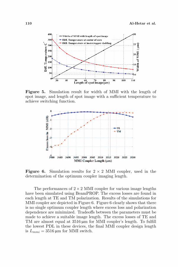
The length of self-image inside MMI region is proportional to thewidth of MMI as shown in Figure 5. Therefore, heater’s length shouldbe smaller than or equal to the length of spot image, in case MMIswitch which uses the heater inside MMI region to change the phase ofimage. So the heater’s length is restricted with a spot image’s length.
Equations (2)–(4) are used to calculate the different temperature(∆T ) which is sufficient to induce a π phase shift in the light travelingthrough position of spot image. If the length of spot image issmall which means that a heater’s length is small, a highly differenttemperature is needed to achieve switching function as shown inFigure 5. Practically, it is impossible to generate high temperature(T > 280◦C) at heater/upper cladding interface to achieve switchingfunction, since the stability of the material will be affected [23].Therefore, a wider width is required to increase the length of the heater,and to generate a smaller temperature than previously mentioned toachieve switching functions. According to that, it is important to dotrade-off between width of MMI and length of a spot image. The width,W = 30 µm is chosen to increase the length of heater (Lh = 110µm)and generate small temperature at heater/upper cladding interface(T = 108◦C) for optimum working condition.
110 Al-Hetar et al.
Figure 5. Simulation result for width of MMI with the length ofspot image, and length of spot image with a sufficient temperature toachieve switching function.
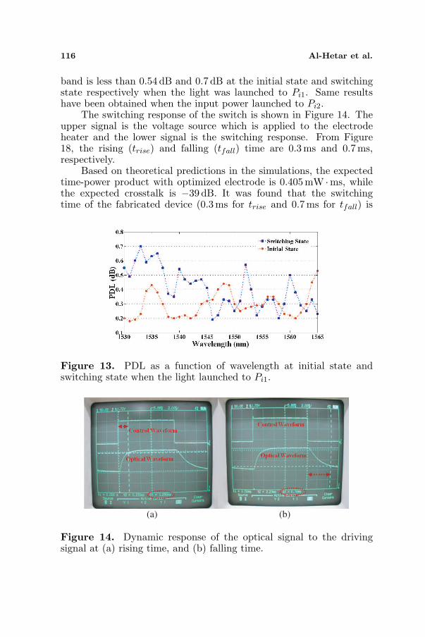
Figure 6. Simulation results for 2 × 2 MMI coupler, used in thedetermination of the optimum coupler imaging length.
The performances of 2× 2 MMI coupler for various image lengthshave been simulated using BeamPROP. The excess losses are found ineach length at TE and TM polarization. Results of the simulations forMMI coupler are depicted in Figure 6. Figure 6 clearly shows that thereis no single optimum coupler length where excess loss and polarizationdependence are minimized. Tradeoffs between the parameters must bemade to achieve a suitable image length. The excess losses of TE andTM are almost equal at 3516µm for MMI coupler’s length. To fulfillthe lowest PDL in these devices, the final MMI coupler design lengthis Lmmi = 3516µm for MMI switch.

Progress In Electromagnetics Research B, Vol. 24, 2010 111
Femlab simulation software from COMSOL is also used. This toolis based on Finite Element Method (FEM) to evaluate the response ofheat transfer from the thin-film heater to the structure’s layers. Thethermal conductivity of Al, Si and polymer (ZPU12-480 and LRF378)are 250Wm−1◦C−1, 163 Wm−1◦C−1, and 0.2 Wm−1◦C−1 respectively.Figure 7 shows the transient temperature response of the electrodeheater and central waveguide of the MMI switch with trench. The risetime (trise) is defined as the time from 10 to 90% ∆T and the fall time(tfall) is defined as the time from 90% to 10% ∆T . The simulated trise
and tfall are 0.3ms, which are also the determined switching times forproposed MMI switch.
Figure 7. Transient thermal state of the proposed MMI switch.
Figure 8. Simulation results based on FD-BPM of channel outputversus driving power MMI switch at the cross state and bar state.

112 Al-Hetar et al.
The optical and thermal behaviors of proposed 2×2 MMI thermo-optic switch were verified by BeamPROP, it is based on FiniteDifference Beam Propagation Method (FD-BPM), and includes theeffects of heater. The changing phase is done by certain value of appliedpower (1.35mW) as shown in Figure 8. The simulation result showsthat the crosstalk (CT) of this structure is −39 dB at the cross stateand bar state.
3. FABRICATION
Three different masks have been used in the fabrication process, onefor the ridge silicon in substrate layer, one for heater electrodes andheater pads structure, and one for the ridge waveguide structure. Theprocesses involved are depicted in Figure 9.
Figure 9. Fabrication steps of polymer thermo-optic switch.

Progress In Electromagnetics Research B, Vol. 24, 2010 113
Firstly, a 4-inch Si wafer serves as a substrate which is coveredby positive photoresist (Si-PR). After a soft bake (1 minute at 90◦C),the ridge Si in substrate is defined through a chromium mask at awavelength of 410 nm (UV light). After development and a hard bakeat 120◦C for 30 minutes, the wafer was etched to form a 3µm ridgeheight by using Inductively Coupled Plasma Etcher (ICPE). ThenLFR378 is spun-coated on the Si substrate as lower cladding. TheLFR378 solution was dispensed onto the center of the ridge silicon,approximately 5ml for a 4-inch substrate. Then the substrate wasspun at 300 rpm for approximately 3–5 seconds to spread the resinout from the center. The substrate was then spun for 20 secondsat spinning speed 2500 rpm to obtain the desired polymer thicknesstarget at 6µm. Next, ZPU12-480 is spun-coated on the lower claddinglayer. The required thickness of this layer is 1µm, so the second speedwas 3000 rpm for 60 seconds to obtain that thickness. Then, LFR378is spun-coated on the core layer as upper cladding. The requiredthickness of this layer is 2µm. So the second speed was 3000 rpmfor 40 seconds to obtain that thickness. After each spinning, the waferwas put in UV chamber for UV curing.
To define the heater electrodes and heater pads, the wafer wascovered by negative photoresist (AZ3612) which is the first step inthe photolithography. The photoresist thickness must be thicker thanthe thickness of the Chromium (Cr) (the Cr layer was introduced asan adhesion) and Al. Then, the heater electrodes and heater padswere applied to the negative photoresist. The photoresist layer waspatterned in a reverse pattern, i.e., the photoresist layer was removedfrom the area where the metals are to remain in final structure as shownin Figure 9. Then, the Cr and Al deposition were consecutively doneby using e-beam evaporation technique [24] over the masking layer andin openings through the masking layer. The lift-off was performed ina Micrchem Remover PG solution to remove the metals overlying thephotoresist layer and leave the desired metal pattern on the underlyingsurface.
To define the ridge waveguide, the wafer was covered byphotoresist which is the first step in the photolithography. Positivephotoresist (Si-PR) has been spun at 3500 rpm for 20 seconds to forma layer of photoresist over the wafer. After a soft bake (1 minute at90◦C), the waveguide, heater electrodes, and heaters pads pattern orwaveguide pattern was defined through a chromium mask by UV light.After development and a hard bake (30 minutes at 120◦C), the waferwas etching to form 4µm of ridge height by using ICPE.

114 Al-Hetar et al.
4. MEASUREMENTS AND DISCUSSION
The experimental setup that was used for all the measurements isshown in Figure 10. The light originated from a tunable laser source(TLS) passed through a polarization controller to choose TE or TMmode and then the light was coupled to the fiber block. The deviceunder test (DUT) was placed on the holder with a vacuum pump andwas controlled manually by the rotational stage with XYZ positioningstages. The output light intensity from the DUT was sent to photodiode (PD) and next to the PC. The microprobes were connected to thepower supply to drive the electrodes. Additionally, the oscilloscope wasconnected to the power supply and PD to show the switching response.
The switch curves were investigated by using the experimentalsetup as shown in Figure 10 which include tunable laser (outputlevel was fixed at 1 mW and wavelength was set to 1550 nm). Therelationship between the driving power inmW and the output levelpower in dBm of each output was measured and shown in Figure 11.
Figure 11 shows the optical power level in the cross port andthe bar port responding to the driving power, when the light waslaunched into Pi1. The switch has a crosstalk of −36.2 dB in the crossstate (initial state), when there is no driving power to the electrodeheater. With driving power increases, the optical power in thecross port decreases but in the bar port will increase simultaneously.Eventually, the switch will reach the bar state (switching state). Here,we define the driven power (applied power to the electrode heater)resulting in maximum optical power in the bar port as the powerconsumption, which is 1.85 mW, achieving a crosstalk of −36.95 dB.For the fabricated switch, the extinction ratio (ER) is higher than36.1 dB.
Figure 10. Experimental setup for device characterization.

Progress In Electromagnetics Research B, Vol. 24, 2010 115
Figure 11. Measured switching curves when light launched into Pi1.
Figure 12. IL as a function of wavelength at initial state and switchingstate when the light launched to Pi1.
Characteristics of the switch within C-band range were done usingthe same experimental setup shown in Figure 10. The references ofthe driving power were set at the initial and switching state, whichare 0 mW and 1.85 mW, respectively. The results were depicted inFigure 12 when the light was launched into Pi1. It can be seen fromFigure 12 that wavelength dependent loss (WDL) of the 2 × 2 MMIoptical switch within C-band is 0.78 dB and 0.88 dB at the initial stateand switching state respectively when the light was launched to Pi1.
The polarization dependent loss (PDL) within C-band range wasmeasured simultaneously. Figure 13 shows the test results when theinput is Pi1 and corresponds to the zero driving power (0 mW) forinitial state and 1.85mW for switching state. It can be seen fromFigure 13 that the PDL of the 2 × 2 MMI optical switch within C-
116 Al-Hetar et al.
band is less than 0.54 dB and 0.7 dB at the initial state and switchingstate respectively when the light was launched to Pi1. Same resultshave been obtained when the input power launched to Pi2.
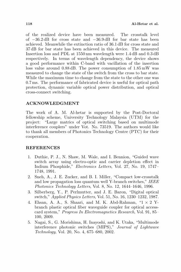
The switching response of the switch is shown in Figure 14. Theupper signal is the voltage source which is applied to the electrodeheater and the lower signal is the switching response. From Figure18, the rising (trise) and falling (tfall) time are 0.3 ms and 0.7 ms,respectively.
Based on theoretical predictions in the simulations, the expectedtime-power product with optimized electrode is 0.405 mW ·ms, whilethe expected crosstalk is −39 dB. It was found that the switchingtime of the fabricated device (0.3ms for trise and 0.7ms for tfall) is
Figure 13. PDL as a function of wavelength at initial state andswitching state when the light launched to Pi1.
(a) (b)
Figure 14. Dynamic response of the optical signal to the drivingsignal at (a) rising time, and (b) falling time.

Progress In Electromagnetics Research B, Vol. 24, 2010 117
Table 1. Comparison of the performance of the fabricated switch inthis work with other published results for polymer based thermo-opticswitch.
In×OutPower-Time product
(mW ·ms)CT (dB) Author
2× 2 88 −31 [25]2× 2 102 −32/−30 [22]2× 2 3 −20/−18 [26]1× 2 192.4 −23 [27]2× 2 1.3 −36.2 Present work
a little slower than the simulation results (0.3 ms for both) especiallythe cooling time, which is possibly caused by approximation of the 2D-FDTM. In addition, the measured power consumption (1.85 mW) is alittle higher than the simulation results (1.35mW), which is possiblycaused by the poor quality of the applied conductive paint connections,resulting in excess power dissipation at the heater contacts. For the2 × 2 MMI described in this work, the switching time-power productis 1.3 mW ·ms. This value is put into perspective by comparison withperformance of the polymer based thermo-optic switches published inthe literature, given in Table 1. It must be noted that the switch isdesigned to meet a number of requirements such as that crosstalk, lowloss, and polarization insensitivity in addition to the efficient thermo-optic operation, so some of the switches in Table 1 have not beenoptimized for these later requirements. The fabricated device has thelowest switching time- power product up to date.
Finally, it is the belief then that the good performance ofthe fabricated device herein is accumulative of materials technology,modified structure, and optimum design. The optical device describedherein with these properties is useful for optical path protection,dynamic variable optical power distribution, and optical cross-connectswitching.
5. CONCLUSION
The 2×2 MMI polymer thermo-optic switch in a high refractive indexcontrast (0.102) with a new structure design has been realized. Thisdevice was fabricated using standard fabrication technique such ascoating, photolithography, and dry etching. The optical properties
118 Al-Hetar et al.
of the realized device have been measured. The crosstalk levelof −36.2 dB for cross state and −36.9 dB for bar state has beenachieved. Meanwhile the extinction ratio of 36.1 dB for cross state and37 dB for bar state has been achieved in this device. The measuredInsertion loss and PDL at 1550 nm wavelength were 1.4 dB and 0.3 dBrespectively. In terms of wavelength dependency, the device showsa good performance within C-band with vacillation of the insertionloss value around 0.88 dB. The power consumption of 1.85 mW wasmeasured to change the state of the switch from the cross to bar state.While the maximum time to change from the state to the other one was0.7ms. The performance of fabricated device is useful for optical pathprotection, dynamic variable optical power distribution, and opticalcross-connect switching.
ACKNOWLEDGMENT
The work of A. M. Al-hetar is supported by the Post-Doctoralfellowship scheme, University Technology Malaysia (UTM) for theproject: “Large matrics of optical switching based on multimodeinterference couplers” under Vot. No. 73519. The authors would liketo thank all members of Photonics Technology Centre (PTC) for theircooperation.
REFERENCES
1. Duthie, P. J., N. Shaw, M. Wale, and I. Bennion, “Guided waveswitch array using electro-optic and carrier depletion effect inIndium Phosphide,” Electronics Letters, Vol. 27, No. 19, 1747–1748, 1991.
2. Sneh, A., J. E. Zucker, and B. I. Miller, “Compact low-crosstalkand low propagation loss quantum well Y-branch switches,” IEEEPhotonics Technology Letters, Vol. 8, No. 12, 1644–1646, 1996.
3. Silberberg, Y., P. Perlmutter, and J. E. Baron, “Digital opticalswitch,” Applied Physics Letters, Vol. 51, No. 16, 1230–1232, 1987.
4. Ehsan, A. A., S. Shaari, and M. K. Abd-Rahman, “1 × 2 Y-branch plastic optical fiber waveguide coupler for optical access-card system,” Progress In Electromagnetics Research, Vol. 91, 85–100, 2009.
5. Nagai, S., G. Morishima, H. Inayoshi, and K. Utaka, “Multimodeinterference photonic switches (MIPS),” Journal of LightwaveTechnology, Vol. 20, No. 4, 675–680, 2002.

Progress In Electromagnetics Research B, Vol. 24, 2010 119
6. Agashe, S. S., K. Shiu, and S. R. Forrest, “Compact polarization-insensitive InGaAsP-InP 2 × 2 optical switch,” IEEE PhotonicsTechnology Letters, Vol. 17, No. 1, 52–54, 2005.
7. Shi, Y. and D. Dai, “Design of compact multimode interferencecoupler based on deeply-etched SiO2 ridge waveguides,” OpticsCommunications, Vol. 271, No. 2, 404–407, 2007.
8. Heaton, J. M., R. M. Jenkins, D. R. Wight, J. T. Parker,J. C. H. Birheck, and K. P. Hilton, “Novel 1-to-N wayintegrated optical beam splitters using symmetric mode mixing inGaAs/AlGaAs multimode waveguides,” Applied Physics Letters,Vol. 61, No. 15, 1754–1756, 1992.
9. Besse, P. A., M. Bachmann, H. Melchior, L. B. Soldano, andM. K. Smit, “Optical bandwidth and fabrication tolerancesof multimode interference couplers,” Journal of LightwaveTechnology, Vol. 12, No. 6, 1004–1009, 1994.
10. Soldano, L. B. and E. C. M. Pennings, “Optical multi-mode interference devices based on self-imaging: Principles andapplications,” Journal of Lightwave Technology, Vol. 13, No. 4,615–627, 1995.
11. Jenkins, R. M., J. M. Heaton, D. R. Wight, J. R. Parker,J. C. Birbeck, G. W. Smith, and K. P. Hilton, “Novel 1×N andN × N integrated optical switches using self-imaging multimodeGaAs/AIGaAs waveguides,” Applied Physics Letters, Vol. 64,No. 6, 684–686, 1994.
12. Diemeer, M. B. J., “Polymer thermo-optic space switches foroptical communications,” Optical Materials, Vol. 9, 192–200, 1998.
13. Leuthold, J. and C. H. Joyner, “Multimode interference couplerswith tunable power splitting ratios,” Journal of LightwaveTechnology, Vol. 19, No. 5, 700–707, 2001.
14. Al-hetar, A. M., I. Yulianti, A. S. M. Supa’at, and A. B. Moham-mad, “Thermo-optic multimode interference switches with air andsilicon trenches,” Optics Communications, Vol. 281, 4653–4657,2008.
15. Al-hetar, A. M., A. S. M. Supa’at, A. B. Mohammad, andI. Yulianti, “Crosstalk improvement of a thermo-optic polymerwaveguide MZI–MMI switch,” Optics Communications, Vol. 281,5764–5767, 2008.
16. Fujisawa, T. and M. Koshiba, “Theoretical investigation ofultrasmall polarization-insensitive 1 × 2 multimode interferencewaveguides based on sandwiched structures,” IEEE PhotonicsTechnology Letters, Vol. 18, No. 11, 1246–1248, 2006.

120 Al-Hetar et al.
17. Kalyanasundaram, N. and P. Muthuchidambaranathan, “Nonlin-ear pulse propagation in a weakly birefringent optical fiber Part 1:Derivation of coupled nonlinear schrodinger equations (cnlse),”Progress In Electromagnetics Research B, Vol. 19, 205–231, 2010.
18. Manning, R. J., A. Antonopoulos, R. L. Roux, and A. E. Kelly,“Experimental measurement of nonlinear polarisation rotation insemiconductor optical amplifiers,” Electronics Letters, Vol. 37,No. 4, 229–230, 2001.
19. Kawachi, M., “Silica waveguides on silicon and their applicationto integrated-optic components,” Optical and Quantum Electron,Vol. 22, No. 5, 391–416, 1990.
20. Lai, Q., W. Hunziker, and H. Melchior, “Low-power compact2 × 2 thermooptic silica on- silicon waveguide switch with fastresponse,” IEEE Photonics Technology Letters, Vol. 10, No. 5,681–683, 1998.
21. Supa’at, A. S. M., M. H. Ibrahim, A. B. Mohammad,N. M. Kassim, and E. Ghazali, “A novel thermooptic polymerswitch based on directional coupler structure,” American Journalof Applied Sciences, Vol. 5, No. 11, 1552–1557, 2008.
22. Al-Hetar, A. M., A. S. M. Supa’at, and A. B. Mohammad,“A ridge waveguide for thermo-optic application,” Progress InElectromagnetics Research Letters, Vol. 6, 1–9, 2009.
23. Ma, H., A. Jen, and L. Dalton, “Polymer-based opticalwaveguides: Materials, processing, and devices,” AdvancedMaterials, Vol. 14, No. 19, 1339–1365. 2002.
24. Cheng, T., G. Drew, B. Gillispie, J. Simko, C. Militello, A. Waldo,and A. Wong, “Vapor deposited thin gold coatings for hightemperature electrical contact,” IEEE Proceedings of the 18thInternational Conference on Electrical Contact, 404–413, Chicago,IL, USA, September 1996.
25. Wang, F., J. Yang, L. Chen, X. Jiang, and M. Wang, “Opticalswitch based on multimode interference coupler,” IEEE PhotonicsTechnology Letters, Vol. 18, No. 2, 421–423, 2006.
26. Gao, L., J. Sun, X. Sun, C. Kang, Y. Yan, and D. Zhang,“Low Switching Power 2 × 2 thermo-optic switch using directultraviolet photolithography process,” Optics Communications,Vol. 282, 4091–4094, 2009.
27. Yulianti, I., A. S. M. Supa’at, S. M. Idrus, and A. M. Al-hetar, “Cosine bend-linear waveguide digital optical switch withparabolic heater,” Optics & Laser Technology, Vol. 42, 180–185,2010.