
A NEW HYBRID ACTIVE NEUTRAL POINT CLAMPED …ijlemr.com/papers/REETA2K16/EE048.pdf · A NEW HYBRID...
17
International Journal of Latest Engineering and Management Research (IJLEMR) ISSN: 2455-4847 www.ijlemr.com || REETA-2K16 ǁ PP. 442-458 www.ijlemr.com 442 | Page A NEW HYBRID ACTIVE NEUTRAL POINT CLAMPED FLYING CAPACITOR MULTILEVEL INVERTER J. Nagaraju, Assistant Professor, SVPCET, Puttur Gowtham Chendra, Assistant Professor, SVCE, Tirupathi ABSTRACT: This paper proposes a new five-level hybrid topology combining features of neutral point clamped and flying capacitor inverters. The proposed topology provides a trade-off between different component counts to achieve a good loss distribution, avoid direct series connection of semiconductor devices, keep the balanced operation of dc-link capacitors while keeping the number of costly components such as capacitors and switches low. The required modulation strategy is developed and the operation of the proposed topology is studied. The features of the proposed topology are investigated and compared to other available topologies. Simulation results are provided to verify the performance of the converter for medium voltage applications. Key words - cascaded H-bridge (CHB), neutral point clamped (NPC), flying capacitor (FC) 1. INTRODUCTION Multilevel inverters have gained interest during the last three decades due to the increasing demand for medium to high voltage converters for a variety of high power applications. Different topologies have been proposed to fit the requirements of different applications. For medium voltage inverters, cascaded H-bridge (CHB), neutral point clamped (NPC), and flying capacitor (FC) are the primary topologies. Among them, NPC and FC provide a common dc-link, which is a strict requirement for many applications. FC inverter uses capacitors to generate output voltage levels. The availability of intra phasal redundant states in this topology can provide both capacitor voltage balancing and power loss distribution among switches. However, increased number of flying capacitors at higher levels that increases the initial cost and maintenance surcharges and decreases the reliability of the inverter along with the capacitor Pre-charge in some applications are the main drawbacks of this topology. NPC inverter uses diodes to clamp the voltage levels generated at the dc-link capacitors to the output. Excessive number of diodes, unbalanced operation of dc-link’s voltage divider capacitors, and uneven distribution of loss among switches are major problems of this topology. Space vector algorithms are available to alleviate the unbalanced loss and capacitor voltage problems based on the inverter operating condition. Active NPC (ANPC) improves the loss distribution of NPC by replacing diodes with active switches providing alternative neutral point path. Hybrid topologies are viable solutions where higher number of levels is required. Combining the advantages of CHB, FC, and NPC, hybrid inverters can provide loss and voltage balancing while keeping the number of components low. Examples of hybrid topologies combining FC and NPC can be found in some of which has already found industrial applications. The 5-level FC-ANPC is an example of hybrid topologies that made its way to the industry. Driven mainly by economy of scale (production levels and the field of high-power drives has been one of the most active areas in development of power electronics in the last decades. Several industrial processes have increased their power-level needs, efficiency), triggering the development of new power semiconductors, converter topologies, and control methods. In high power, applications that require high voltages and high currents the maximum ratings of power semiconductors become a real handicap. The series connection of power switches is the solution for dealing with larger voltages. Nevertheless, achieving static and dynamic voltage sharing among those switches becomes a problem, which led to the development of the new family of multilevel converters. On the other hand, paralleling of subsystems is the solution for dealing with larger currents. If more than three phases are used to deliver power to the load then the per-phase current rating is lower and low-current devices can be used. As a consequence, multiphase multilevel converters are good candidates to be used in high- power drive applications. Nevertheless, this advantage comes at the price of a greater complexity in the inverter and in an increased control difficulty. The number of devices that must be controlled goes up from the only six switches of the two-level three-phase converters to the tens of switches of multiphase multilevel converters. At present, there are no commercial digital signal processors (DSPs) having enough appropriate built-in pulse-
-
Upload
truongthuy -
Category
Documents
-
view
224 -
download
3
Transcript of A NEW HYBRID ACTIVE NEUTRAL POINT CLAMPED …ijlemr.com/papers/REETA2K16/EE048.pdf · A NEW HYBRID...
International Journal of Latest Engineering and Management Research (IJLEMR)
ISSN: 2455-4847
www.ijlemr.com || REETA-2K16 ǁ PP. 442-458
www.ijlemr.com 442 | Page
A NEW HYBRID ACTIVE NEUTRAL POINT CLAMPED
FLYING CAPACITOR MULTILEVEL INVERTER
J. Nagaraju, Assistant Professor, SVPCET, Puttur
Gowtham Chendra, Assistant Professor, SVCE, Tirupathi
ABSTRACT: This paper proposes a new five-level hybrid topology combining features of neutral point
clamped and flying capacitor inverters. The proposed topology provides a trade-off between different
component counts to achieve a good loss distribution, avoid direct series connection of semiconductor devices,
keep the balanced operation of dc-link capacitors while keeping the number of costly components such as
capacitors and switches low. The required modulation strategy is developed and the operation of the proposed
topology is studied. The features of the proposed topology are investigated and compared to other available
topologies. Simulation results are provided to verify the performance of the converter for medium voltage
applications.
Key words - cascaded H-bridge (CHB), neutral point clamped (NPC), flying capacitor (FC)
1. INTRODUCTION Multilevel inverters have gained interest during the last three decades due to the increasing demand for
medium to high voltage converters for a variety of high power applications. Different topologies have been
proposed to fit the requirements of different applications. For medium voltage inverters, cascaded H-bridge
(CHB), neutral point clamped (NPC), and flying capacitor (FC) are the primary topologies. Among them, NPC
and FC provide a common dc-link, which is a strict requirement for many applications. FC inverter uses
capacitors to generate output voltage levels. The availability of intra phasal redundant states in this topology can
provide both capacitor voltage balancing and power loss distribution among switches. However, increased
number of flying capacitors at higher levels that increases the initial cost and maintenance surcharges and
decreases the reliability of the inverter along with the capacitor Pre-charge in some applications are the main
drawbacks of this topology.
NPC inverter uses diodes to clamp the voltage levels generated at the dc-link capacitors to the output.
Excessive number of diodes, unbalanced operation of dc-link’s voltage divider capacitors, and uneven
distribution of loss among switches are major problems of this topology. Space vector algorithms are available
to alleviate the unbalanced loss and capacitor voltage problems based on the inverter operating condition. Active
NPC (ANPC) improves the loss distribution of NPC by replacing diodes with active switches providing
alternative neutral point path. Hybrid topologies are viable solutions where higher number of levels is required.
Combining the advantages of CHB, FC, and NPC, hybrid inverters can provide loss and voltage balancing while
keeping the number of components low. Examples of hybrid topologies combining FC and NPC can be found in
some of which has already found industrial applications. The 5-level FC-ANPC is an example of hybrid
topologies that made its way to the industry.
Driven mainly by economy of scale (production levels and the field of high-power drives has been one
of the most active areas in development of power electronics in the last decades. Several industrial processes
have increased their power-level needs, efficiency), triggering the development of new power semiconductors,
converter topologies, and control methods.
In high power, applications that require high voltages and high currents the maximum ratings of power
semiconductors become a real handicap. The series connection of power switches is the solution for dealing
with larger voltages. Nevertheless, achieving static and dynamic voltage sharing among those switches becomes
a problem, which led to the development of the new family of multilevel converters.
On the other hand, paralleling of subsystems is the solution for dealing with larger currents. If more
than three phases are used to deliver power to the load then the per-phase current rating is lower and low-current
devices can be used. As a consequence, multiphase multilevel converters are good candidates to be used in high-
power drive applications. Nevertheless, this advantage comes at the price of a greater complexity in the inverter
and in an increased control difficulty. The number of devices that must be controlled goes up from the only six
switches of the two-level three-phase converters to the tens of switches of multiphase multilevel converters. At
present, there are no commercial digital signal processors (DSPs) having enough appropriate built-in pulse-
International Journal of Latest Engineering and Management Research (IJLEMR)
ISSN: 2455-4847
www.ijlemr.com || REETA-2K16 ǁ PP. 442-458
www.ijlemr.com 443 | Page
width modulation (PWM) units to control all those switches and a software implementation of them is very
time-consuming. The field programmable gate arrays (FPGAs) are the best candidates for the modulation
implementation of multiphase multilevel converters due to their concurrent processing capability and their high
number of output pins.
2. MULTI PHASE MULTILEVEL INVERTERS 2.1 Introduction
Multilevel inverter technology has emerged recently as a very important alternative in the area of high-
power medium-voltage energy control. This chapter presents the most important topology of cascaded multi-cell
with separate dc sources. Emerging topologies like asymmetric hybrid cells and soft-switched multilevel
inverters are also discussed.
In recent years, industry has begun to demand higher power equipment, which now reaches the
megawatt level. Controlled ac drives in the megawatt range are usually connected to the medium-voltage
network. Today, it is hard to connect a single power semiconductor switch directly to medium voltage grids
(2.3, 3.3, 4.16, or 6.9 kV). For these reasons, a new family of multilevel inverters has emerged as the solution
for working with higher voltage levels.
Multilevel inverters include an array of power semiconductors and capacitor voltage sources, the
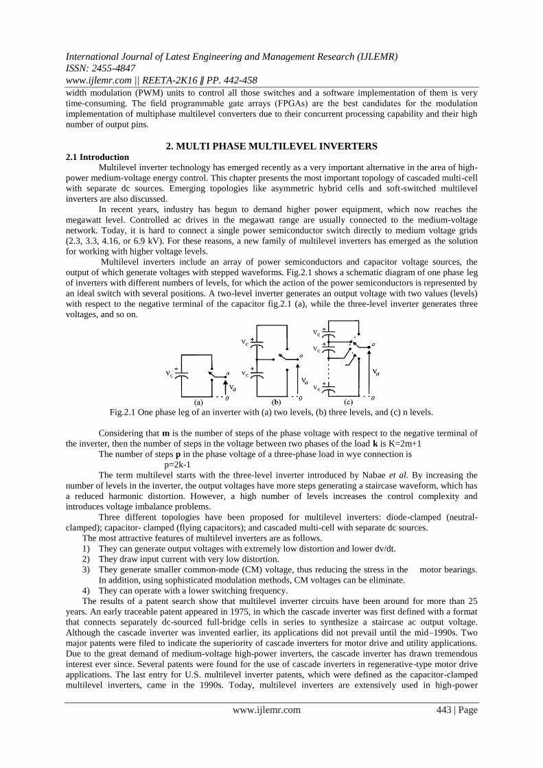
output of which generate voltages with stepped waveforms. Fig.2.1 shows a schematic diagram of one phase leg
of inverters with different numbers of levels, for which the action of the power semiconductors is represented by
an ideal switch with several positions. A two-level inverter generates an output voltage with two values (levels)
with respect to the negative terminal of the capacitor fig.2.1 (a), while the three-level inverter generates three
voltages, and so on.
Fig.2.1 One phase leg of an inverter with (a) two levels, (b) three levels, and (c) n levels.
Considering that m is the number of steps of the phase voltage with respect to the negative terminal of
the inverter, then the number of steps in the voltage between two phases of the load k is K=2m+1
The number of steps p in the phase voltage of a three-phase load in wye connection is
p=2k-1
The term multilevel starts with the three-level inverter introduced by Nabae et al. By increasing the
number of levels in the inverter, the output voltages have more steps generating a staircase waveform, which has
a reduced harmonic distortion. However, a high number of levels increases the control complexity and
introduces voltage imbalance problems.
Three different topologies have been proposed for multilevel inverters: diode-clamped (neutral-
clamped); capacitor- clamped (flying capacitors); and cascaded multi-cell with separate dc sources.
The most attractive features of multilevel inverters are as follows.
1) They can generate output voltages with extremely low distortion and lower dv/dt.
2) They draw input current with very low distortion.
3) They generate smaller common-mode (CM) voltage, thus reducing the stress in the motor bearings.
In addition, using sophisticated modulation methods, CM voltages can be eliminate.
4) They can operate with a lower switching frequency.
The results of a patent search show that multilevel inverter circuits have been around for more than 25
years. An early traceable patent appeared in 1975, in which the cascade inverter was first defined with a format
that connects separately dc-sourced full-bridge cells in series to synthesize a staircase ac output voltage.
Although the cascade inverter was invented earlier, its applications did not prevail until the mid–1990s. Two
major patents were filed to indicate the superiority of cascade inverters for motor drive and utility applications.
Due to the great demand of medium-voltage high-power inverters, the cascade inverter has drawn tremendous
interest ever since. Several patents were found for the use of cascade inverters in regenerative-type motor drive
applications. The last entry for U.S. multilevel inverter patents, which were defined as the capacitor-clamped
multilevel inverters, came in the 1990s. Today, multilevel inverters are extensively used in high-power
International Journal of Latest Engineering and Management Research (IJLEMR)
ISSN: 2455-4847
www.ijlemr.com || REETA-2K16 ǁ PP. 442-458
www.ijlemr.com 444 | Page
applications with medium voltage levels. The field applications include use in laminators, mills, conveyors,
pumps, fans, blowers, compressors, and so on.
2.2 Inverter topologies
2.2.1 Diode-clamped inverter A three-level diode-clamped inverter is shown in Fig.2.2 (a). In this circuit, the dc-bus voltage is split
into three levels by two series-connected bulk capacitors, C1 and C2 . The middle point of the two capacitors n
can be defined as the neutral point. The output voltage Van has three states: Vdc/2 , 0, and –Vdc/2 . For voltage
level Vdc/2 , switches S1and S2 need to be turned on; for –Vdc/2 , switchesS1’ and S2
’ need to be turned on; and
for the 0 level, S2 and S1’ need to be turned on.
Fig.2.2 Diode-clamped multilevel inverter circuit topologies (a) Three-level.(b) Five-level.
The key components that distinguish this circuit from a conventional two-level inverter are D1 and D1’.
These two diodes clamp the switch voltage to half the level of the dc-bus voltage. When both S1 and S2 turn on,
the voltage across a and 0 is Vdc, i.e., va0=Vdc . In this case, D1’ balances out the voltage sharing between S1
’ and
S2’ with S1
’ blocking the voltage across C1 and S2
’blocking the voltage across C2. Notice that output voltage van
is ac, va0 and is dc. The difference between van and va0 is the voltage across C2, which is Vdc/2. If the output is
removed out between a and 0, then the circuit becomes a dc/dc converter, which has three output voltage levels:
Vdc, Vdc/2, and 0.
Fig.2.2 (b) shows a five-level diode-clamped converter in which the dc bus consists of four capacitors,
C1, C2, C3 , and C4. For dc-bus voltage Vdc , the voltage across each capacitor is Vdc/4, and each device voltage
stress will be limited to one capacitor voltage level Vdc /4 through clamping diodes.
To explain how the staircase voltage is synthesized, the neutral point nis considered as the output phase
voltage reference point. There are five switch combinations to synthesize five level voltages across aand n.
1) For voltage level Van=Vdc/2, turn on all upper switches S1–S4.
2) For voltage level Van=Vdc/4, turn on three upper switches S2–S4 and one lower switch S1’.
3) For voltage level Van=0, turn on two upper switches S3and S4 and two lower switches S1’ and S2
’.
4) For voltage level Van= -Vdc/4, turn on one upper switch S4 and three lower switches S1’– S3
’.
5) For voltage level Van= -Vdc/2, turn on all lower switches S1’–S4
’.
Four complementary switch pairs exist in each phase. The complementary switch pair is defined such
that turning on one of the switches will exclude the other from being turned on. In this example, the four
complementary pairs are (S1,S1’ ), (S2,S2
’ ), (S3,S3
’ ), and (S4,S4
’ ).
Although each active switching device is only required to block a voltage level of Vdc/(m-1), the clamping
diodes must have different voltage ratings for reverse voltage blocking. Using D1’ of Fig.3.2(b) as an example,
when lower devices are S2’ ~ S4
’ turned on, D1
’ needs to block three capacitor voltages, or 3Vdc/4. Similarly, D2
and D2’need to block 2Vdc/4, and Da3 needs to block 3Vdc/4. Assuming that each blocking diode voltage rating is
the same as the active device voltage rating, the number of diodes required for each phase will be (m-1)×(m-2) .
This number represents a quadratic increase in m. When m is sufficiently high, the number of diodes required
will make the system impractical to implement. If the inverter runs under PWM, the diode reverse recovery of
these clamping diodes becomes the major design challenge in high-voltage high-power applications.
International Journal of Latest Engineering and Management Research (IJLEMR)
ISSN: 2455-4847
www.ijlemr.com || REETA-2K16 ǁ PP. 442-458
www.ijlemr.com 445 | Page
2.2.2 Capacitor-clamped inverter
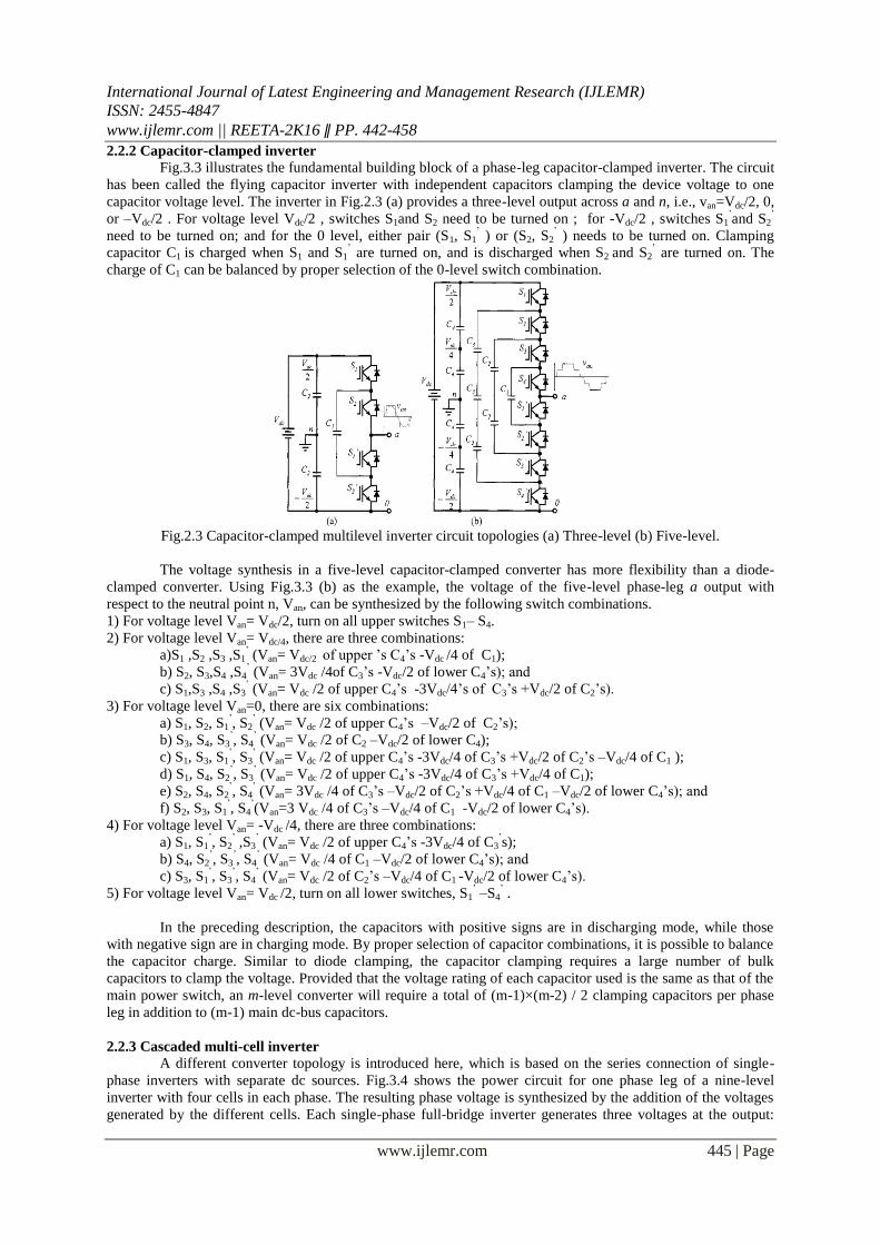
Fig.3.3 illustrates the fundamental building block of a phase-leg capacitor-clamped inverter. The circuit
has been called the flying capacitor inverter with independent capacitors clamping the device voltage to one
capacitor voltage level. The inverter in Fig.2.3 (a) provides a three-level output across a and n, i.e., van=Vdc/2, 0,
or –Vdc/2 . For voltage level Vdc/2 , switches S1and S2 need to be turned on ; for -Vdc/2 , switches S1’and S2
’
need to be turned on; and for the 0 level, either pair (S1, S1’ ) or (S2, S2
’ ) needs to be turned on. Clamping
capacitor C1 is charged when S1 and S1’ are turned on, and is discharged when S2 and S2
’ are turned on. The
charge of C1 can be balanced by proper selection of the 0-level switch combination.
Fig.2.3 Capacitor-clamped multilevel inverter circuit topologies (a) Three-level (b) Five-level.
The voltage synthesis in a five-level capacitor-clamped converter has more flexibility than a diode-
clamped converter. Using Fig.3.3 (b) as the example, the voltage of the five-level phase-leg a output with
respect to the neutral point n, Van, can be synthesized by the following switch combinations.
1) For voltage level Van= Vdc/2, turn on all upper switches S1– S4.
2) For voltage level Van= Vdc/4, there are three combinations:
a)S1 ,S2 ,S3 ,S1’ (Van= Vdc/2 of upper ’s C4’s -Vdc /4 of C1);
b) S2, S3,S4 ,S4’ (Van= 3Vdc /4of C3’s -Vdc/2 of lower C4’s); and
c) S1,S3 ,S4 ,S3’ (Van= Vdc /2 of upper C4’s -3Vdc/4’s of C3’s +Vdc/2 of C2’s).
3) For voltage level Van=0, there are six combinations:
a) S1, S2, S1’, S2
’ (Van= Vdc /2 of upper C4’s –Vdc/2 of C2’s);
b) S3, S4, S3’, S4
’ (Van= Vdc /2 of C2 –Vdc/2 of lower C4);
c) S1, S3, S1’, S3
’ (Van= Vdc /2 of upper C4’s -3Vdc/4 of C3’s +Vdc/2 of C2’s –Vdc/4 of C1 );
d) S1, S4, S2’, S3
’ (Van= Vdc /2 of upper C4’s -3Vdc/4 of C3’s +Vdc/4 of C1);
e) S2, S4, S2’, S4
’ (Van= 3Vdc /4 of C3’s –Vdc/2 of C2’s +Vdc/4 of C1 –Vdc/2 of lower C4’s); and
f) S2, S3, S1’, S4
’(Van=3 Vdc /4 of C3’s –Vdc/4 of C1 -Vdc/2 of lower C4’s).
4) For voltage level Van= -Vdc /4, there are three combinations:
a) S1, S1’, S2
’ ,S3
’ (Van= Vdc /2 of upper C4’s -3Vdc/4 of C3
’s);
b) S4, S2’, S3
’, S4
’ (Van= Vdc /4 of C1 –Vdc/2 of lower C4’s); and
c) S3, S1’, S3
’, S4
’ (Van= Vdc /2 of C2’s –Vdc/4 of C1 -Vdc/2 of lower C4’s).
5) For voltage level Van= Vdc /2, turn on all lower switches, S1’ –S4
’ .
In the preceding description, the capacitors with positive signs are in discharging mode, while those
with negative sign are in charging mode. By proper selection of capacitor combinations, it is possible to balance
the capacitor charge. Similar to diode clamping, the capacitor clamping requires a large number of bulk
capacitors to clamp the voltage. Provided that the voltage rating of each capacitor used is the same as that of the
main power switch, an m-level converter will require a total of (m-1)×(m-2) / 2 clamping capacitors per phase
leg in addition to (m-1) main dc-bus capacitors.
2.2.3 Cascaded multi-cell inverter A different converter topology is introduced here, which is based on the series connection of single-
phase inverters with separate dc sources. Fig.3.4 shows the power circuit for one phase leg of a nine-level
inverter with four cells in each phase. The resulting phase voltage is synthesized by the addition of the voltages
generated by the different cells. Each single-phase full-bridge inverter generates three voltages at the output:
International Journal of Latest Engineering and Management Research (IJLEMR)
ISSN: 2455-4847
www.ijlemr.com || REETA-2K16 ǁ PP. 442-458
www.ijlemr.com 446 | Page
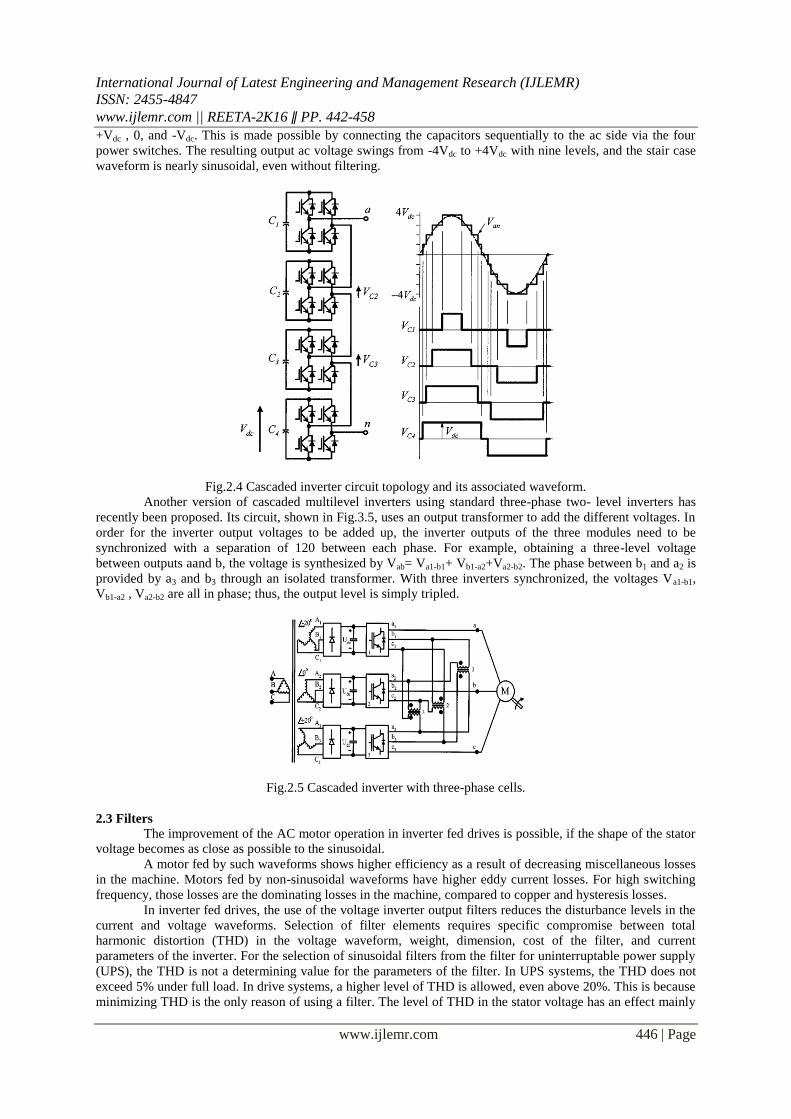
+Vdc , 0, and -Vdc. This is made possible by connecting the capacitors sequentially to the ac side via the four
power switches. The resulting output ac voltage swings from -4Vdc to +4Vdc with nine levels, and the stair case
waveform is nearly sinusoidal, even without filtering.
Fig.2.4 Cascaded inverter circuit topology and its associated waveform.
Another version of cascaded multilevel inverters using standard three-phase two- level inverters has
recently been proposed. Its circuit, shown in Fig.3.5, uses an output transformer to add the different voltages. In
order for the inverter output voltages to be added up, the inverter outputs of the three modules need to be
synchronized with a separation of 120 between each phase. For example, obtaining a three-level voltage
between outputs aand b, the voltage is synthesized by Vab= Va1-b1+ Vb1-a2+Va2-b2. The phase between b1 and a2 is
provided by a3 and b3 through an isolated transformer. With three inverters synchronized, the voltages Va1-b1,
Vb1-a2 , Va2-b2 are all in phase; thus, the output level is simply tripled.
Fig.2.5 Cascaded inverter with three-phase cells.
2.3 Filters
The improvement of the AC motor operation in inverter fed drives is possible, if the shape of the stator
voltage becomes as close as possible to the sinusoidal.
A motor fed by such waveforms shows higher efficiency as a result of decreasing miscellaneous losses
in the machine. Motors fed by non-sinusoidal waveforms have higher eddy current losses. For high switching
frequency, those losses are the dominating losses in the machine, compared to copper and hysteresis losses.
In inverter fed drives, the use of the voltage inverter output filters reduces the disturbance levels in the
current and voltage waveforms. Selection of filter elements requires specific compromise between total
harmonic distortion (THD) in the voltage waveform, weight, dimension, cost of the filter, and current
parameters of the inverter. For the selection of sinusoidal filters from the filter for uninterruptable power supply
(UPS), the THD is not a determining value for the parameters of the filter. In UPS systems, the THD does not
exceed 5% under full load. In drive systems, a higher level of THD is allowed, even above 20%. This is because
minimizing THD is the only reason of using a filter. The level of THD in the stator voltage has an effect mainly
International Journal of Latest Engineering and Management Research (IJLEMR)
ISSN: 2455-4847
www.ijlemr.com || REETA-2K16 ǁ PP. 442-458
www.ijlemr.com 447 | Page
on the motor efficiency. Since one additional reason for using a filter in drive systems is to avoid voltage wave
reflection on the motor terminals, a filter with a THD higher than 5% may probably fit the set tasks while being
economically acceptable. It is important to note that the transistors’ switching frequency has a significant effect
on the value of filter inductances and capacitances. This switching frequency is much lower in drive systems
than in UPS systems
The output voltage quality at the inverter side can be improved by using active and passive filters.
Today, passive filtering is widely used at the output of the inverter to improve the voltage waveform. Such
filters are hardware circuits that are installed on the output of the converter structure. The most common
approach is the use of filters based on resistors, inductors, and capacitors (LC filters). In order to reduce the
over-voltages that can occur, because of wave reflection at the motor terminals when long cables are used,
differential mode LC filters are used. The cable length is important in determining the output performance of the
drive system; however, the cable layout on the user end is generally unknown to the inverter manufacturer.
Moreover, such filters components are decided according to the switching frequency of the inverter. When an
inverter output filter is installed in the electric drive, the voltage drops and the phase shifts between the filter’s
input while output voltages and currents appear. This complicates the control system design, particularly for low
speed conditions. The control systems are generally designed assuming the inverter’s output voltages and
currents are equal to the motor input values. In the case of a discrepancy between voltages and currents, the
region of proper motor operation is limited. Therefore, in a control system of electric drives with an inverter
output filter, it is essential to provide modification in the measurement circuits or in the control algorithms. A
simple way to improve the performance of the electric drive with inverter output filter is to introduce additional
sensors for motor voltages and current measurements. Such a solution is not practical because it requires
changes in the inverter structure so, in this case, an accepted solution is to keep the inverter structure unchanged
but to modify a control algorithm.
III. MULTILEVEL CONVERTER SWITCHING STRATEGIES An inverter is an electrical device that converts direct current (DC) to alternating current (AC); the
converted AC can be at any required voltage and frequency with the use of appropriate transformers, switching,
and control circuits.
Static inverters have no moving parts and are used in a wide range of applications, from small
switching power supplies in computers, to large electric utilityhigh-voltage direct current applications that
transport bulk power. Inverters are commonly used to supply AC power from DC sources such as solar panels or
batteries.
The electrical inverter is a high-power electronic oscillator. It is so named because early mechanical
AC to DC converters was made to work in reverse, and thus were "inverted", to convert DC to AC.
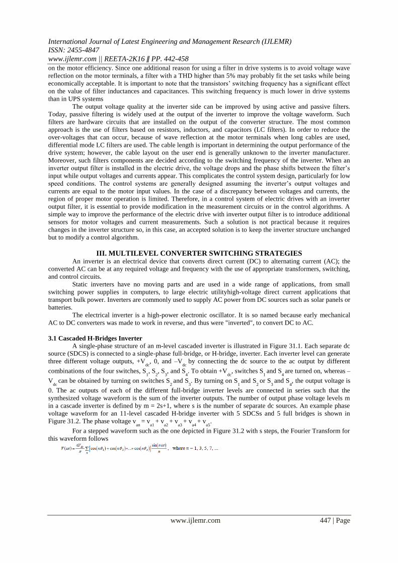
3.1 Cascaded H-Bridges Inverter
A single-phase structure of an m-level cascaded inverter is illustrated in Figure 31.1. Each separate dc
source (SDCS) is connected to a single-phase full-bridge, or H-bridge, inverter. Each inverter level can generate
three different voltage outputs, +Vdc
, 0, and –Vdc
by connecting the dc source to the ac output by different
combinations of the four switches, S1, S
2, S
3, and S
4. To obtain +V
dc, switches S
1 and S
4 are turned on, whereas –
Vdc
can be obtained by turning on switches S2 and S
3. By turning on S
1 and S
2 or S
3 and S
4, the output voltage is
0. The ac outputs of each of the different full-bridge inverter levels are connected in series such that the
synthesized voltage waveform is the sum of the inverter outputs. The number of output phase voltage levels m
in a cascade inverter is defined by m = 2s+1, where s is the number of separate dc sources. An example phase
voltage waveform for an 11-level cascaded H-bridge inverter with 5 SDCSs and 5 full bridges is shown in
Figure 31.2. The phase voltage van
= va1
+ va2
+ va3
+ va4
+ va5
.
For a stepped waveform such as the one depicted in Figure 31.2 with s steps, the Fourier Transform for
this waveform follows
International Journal of Latest Engineering and Management Research (IJLEMR)
ISSN: 2455-4847
www.ijlemr.com || REETA-2K16 ǁ PP. 442-458
www.ijlemr.com 448 | Page
Fig.3.1 Single-phase structure of a multilevel cascaded H-bridges inverter The magnitudes of the Fourier
coefficients when normalized with respect to Vdc
are as follows:
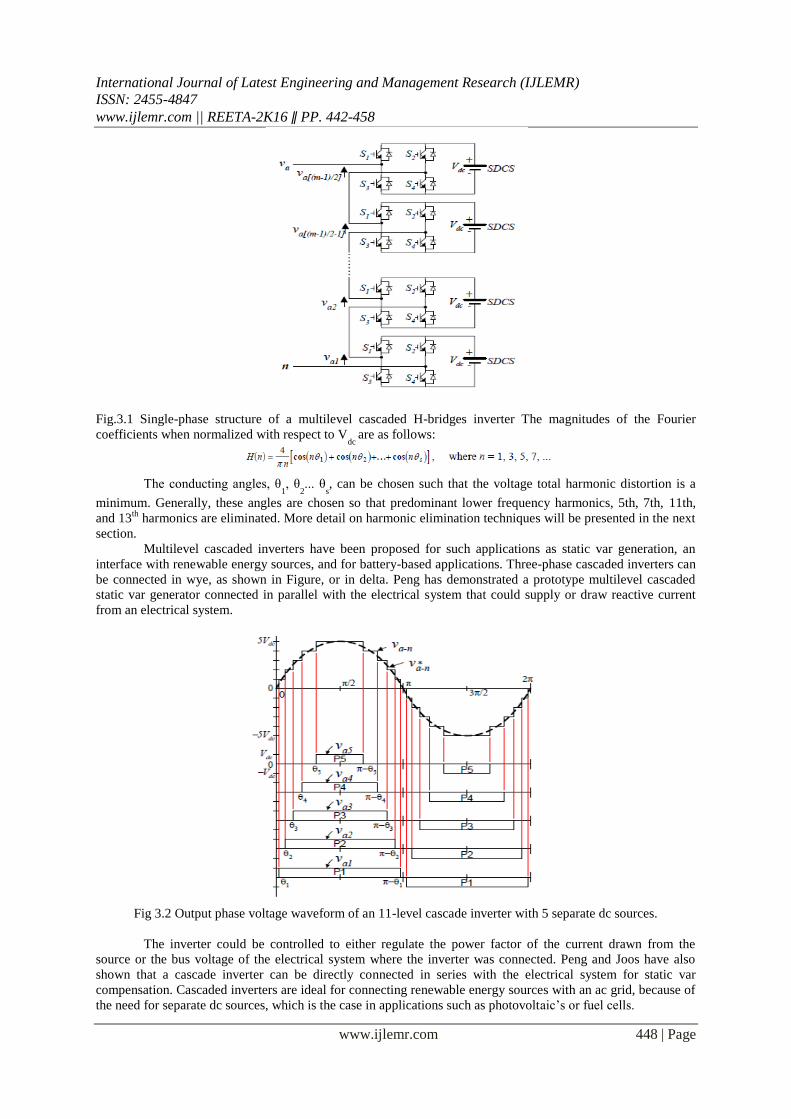
The conducting angles, θ
1, θ
2... θ
s, can be chosen such that the voltage total harmonic distortion is a
minimum. Generally, these angles are chosen so that predominant lower frequency harmonics, 5th, 7th, 11th,
and 13th
harmonics are eliminated. More detail on harmonic elimination techniques will be presented in the next
section.
Multilevel cascaded inverters have been proposed for such applications as static var generation, an
interface with renewable energy sources, and for battery-based applications. Three-phase cascaded inverters can
be connected in wye, as shown in Figure, or in delta. Peng has demonstrated a prototype multilevel cascaded
static var generator connected in parallel with the electrical system that could supply or draw reactive current
from an electrical system.
Fig 3.2 Output phase voltage waveform of an 11-level cascade inverter with 5 separate dc sources.
The inverter could be controlled to either regulate the power factor of the current drawn from the
source or the bus voltage of the electrical system where the inverter was connected. Peng and Joos have also
shown that a cascade inverter can be directly connected in series with the electrical system for static var
compensation. Cascaded inverters are ideal for connecting renewable energy sources with an ac grid, because of
the need for separate dc sources, which is the case in applications such as photovoltaic’s or fuel cells.
International Journal of Latest Engineering and Management Research (IJLEMR)
ISSN: 2455-4847
www.ijlemr.com || REETA-2K16 ǁ PP. 442-458
www.ijlemr.com 449 | Page
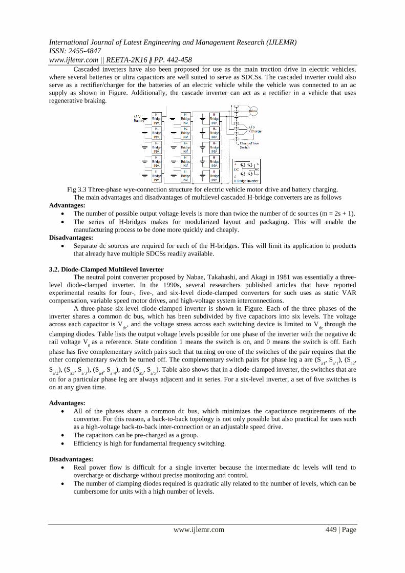
Cascaded inverters have also been proposed for use as the main traction drive in electric vehicles,
where several batteries or ultra capacitors are well suited to serve as SDCSs. The cascaded inverter could also
serve as a rectifier/charger for the batteries of an electric vehicle while the vehicle was connected to an ac
supply as shown in Figure. Additionally, the cascade inverter can act as a rectifier in a vehicle that uses
regenerative braking.
Fig 3.3 Three-phase wye-connection structure for electric vehicle motor drive and battery charging.
The main advantages and disadvantages of multilevel cascaded H-bridge converters are as follows
Advantages:
The number of possible output voltage levels is more than twice the number of dc sources (m = 2s + 1).
The series of H-bridges makes for modularized layout and packaging. This will enable the
manufacturing process to be done more quickly and cheaply.
Disadvantages:
Separate dc sources are required for each of the H-bridges. This will limit its application to products
that already have multiple SDCSs readily available.
3.2. Diode-Clamped Multilevel Inverter
The neutral point converter proposed by Nabae, Takahashi, and Akagi in 1981 was essentially a three-
level diode-clamped inverter. In the 1990s, several researchers published articles that have reported
experimental results for four-, five-, and six-level diode-clamped converters for such uses as static VAR
compensation, variable speed motor drives, and high-voltage system interconnections.
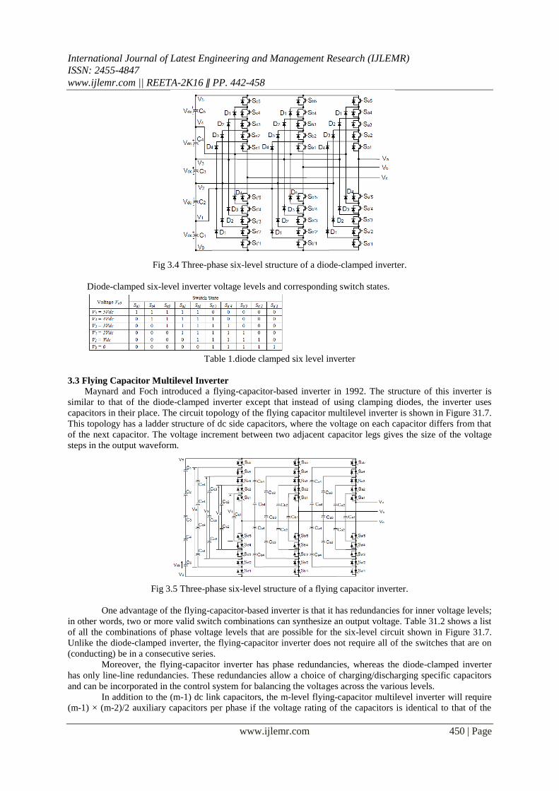
A three-phase six-level diode-clamped inverter is shown in Figure. Each of the three phases of the
inverter shares a common dc bus, which has been subdivided by five capacitors into six levels. The voltage
across each capacitor is Vdc
, and the voltage stress across each switching device is limited to Vdc
through the
clamping diodes. Table lists the output voltage levels possible for one phase of the inverter with the negative dc
rail voltage V0
as a reference. State condition 1 means the switch is on, and 0 means the switch is off. Each
phase has five complementary switch pairs such that turning on one of the switches of the pair requires that the
other complementary switch be turned off. The complementary switch pairs for phase leg a are (Sa1
, Sa’1
), (Sa2
,
Sa’2
), (Sa3
, Sa’3
), (Sa4
, Sa’4
), and (Sa5
, Sa’5
). Table also shows that in a diode-clamped inverter, the switches that are
on for a particular phase leg are always adjacent and in series. For a six-level inverter, a set of five switches is
on at any given time.
Advantages:
All of the phases share a common dc bus, which minimizes the capacitance requirements of the
converter. For this reason, a back-to-back topology is not only possible but also practical for uses such
as a high-voltage back-to-back inter-connection or an adjustable speed drive.
The capacitors can be pre-charged as a group.
Efficiency is high for fundamental frequency switching.
Disadvantages:
Real power flow is difficult for a single inverter because the intermediate dc levels will tend to
overcharge or discharge without precise monitoring and control.
The number of clamping diodes required is quadratic ally related to the number of levels, which can be
cumbersome for units with a high number of levels.
International Journal of Latest Engineering and Management Research (IJLEMR)
ISSN: 2455-4847
www.ijlemr.com || REETA-2K16 ǁ PP. 442-458
www.ijlemr.com 450 | Page
Fig 3.4 Three-phase six-level structure of a diode-clamped inverter.
Diode-clamped six-level inverter voltage levels and corresponding switch states.
Table 1.diode clamped six level inverter
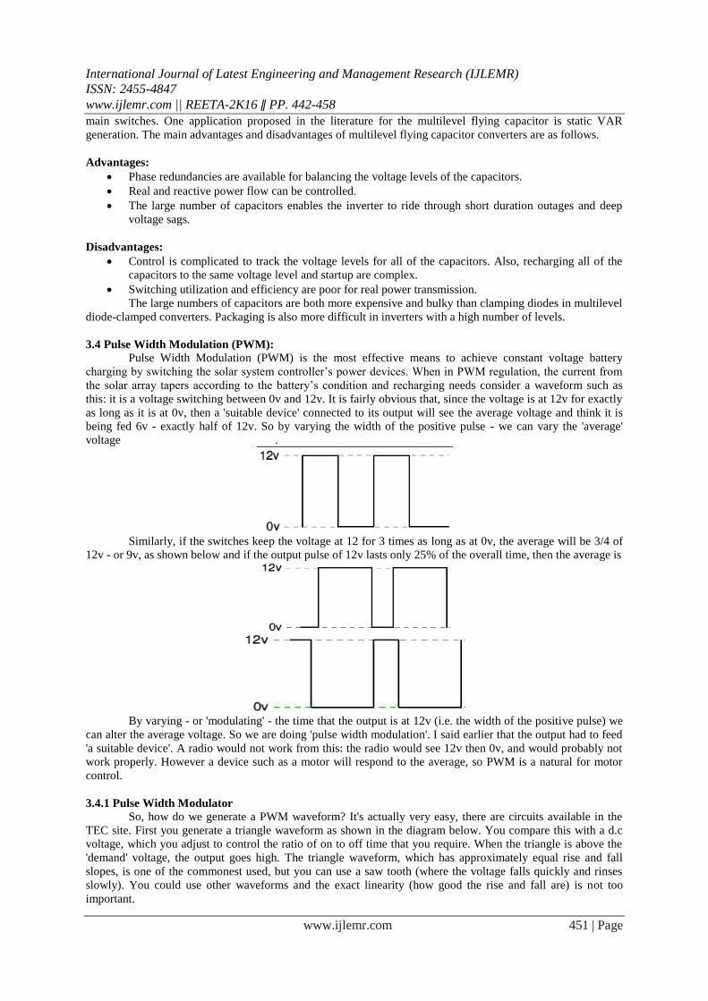
3.3 Flying Capacitor Multilevel Inverter
Maynard and Foch introduced a flying-capacitor-based inverter in 1992. The structure of this inverter is
similar to that of the diode-clamped inverter except that instead of using clamping diodes, the inverter uses
capacitors in their place. The circuit topology of the flying capacitor multilevel inverter is shown in Figure 31.7.
This topology has a ladder structure of dc side capacitors, where the voltage on each capacitor differs from that
of the next capacitor. The voltage increment between two adjacent capacitor legs gives the size of the voltage
steps in the output waveform.
Fig 3.5 Three-phase six-level structure of a flying capacitor inverter.
One advantage of the flying-capacitor-based inverter is that it has redundancies for inner voltage levels;
in other words, two or more valid switch combinations can synthesize an output voltage. Table 31.2 shows a list
of all the combinations of phase voltage levels that are possible for the six-level circuit shown in Figure 31.7.
Unlike the diode-clamped inverter, the flying-capacitor inverter does not require all of the switches that are on
(conducting) be in a consecutive series.
Moreover, the flying-capacitor inverter has phase redundancies, whereas the diode-clamped inverter
has only line-line redundancies. These redundancies allow a choice of charging/discharging specific capacitors
and can be incorporated in the control system for balancing the voltages across the various levels.
In addition to the (m-1) dc link capacitors, the m-level flying-capacitor multilevel inverter will require
(m-1) × (m-2)/2 auxiliary capacitors per phase if the voltage rating of the capacitors is identical to that of the
International Journal of Latest Engineering and Management Research (IJLEMR)
ISSN: 2455-4847
www.ijlemr.com || REETA-2K16 ǁ PP. 442-458
www.ijlemr.com 451 | Page
main switches. One application proposed in the literature for the multilevel flying capacitor is static VAR
generation. The main advantages and disadvantages of multilevel flying capacitor converters are as follows.
Advantages:
Phase redundancies are available for balancing the voltage levels of the capacitors.
Real and reactive power flow can be controlled.
The large number of capacitors enables the inverter to ride through short duration outages and deep
voltage sags.
Disadvantages:
Control is complicated to track the voltage levels for all of the capacitors. Also, recharging all of the
capacitors to the same voltage level and startup are complex.
Switching utilization and efficiency are poor for real power transmission.
The large numbers of capacitors are both more expensive and bulky than clamping diodes in multilevel
diode-clamped converters. Packaging is also more difficult in inverters with a high number of levels.
3.4 Pulse Width Modulation (PWM):
Pulse Width Modulation (PWM) is the most effective means to achieve constant voltage battery
charging by switching the solar system controller’s power devices. When in PWM regulation, the current from
the solar array tapers according to the battery’s condition and recharging needs consider a waveform such as
this: it is a voltage switching between 0v and 12v. It is fairly obvious that, since the voltage is at 12v for exactly
as long as it is at 0v, then a 'suitable device' connected to its output will see the average voltage and think it is
being fed 6v - exactly half of 12v. So by varying the width of the positive pulse - we can vary the 'average'
voltage .
Similarly, if the switches keep the voltage at 12 for 3 times as long as at 0v, the average will be 3/4 of
12v - or 9v, as shown below and if the output pulse of 12v lasts only 25% of the overall time, then the average is
By varying - or 'modulating' - the time that the output is at 12v (i.e. the width of the positive pulse) we
can alter the average voltage. So we are doing 'pulse width modulation'. I said earlier that the output had to feed
'a suitable device'. A radio would not work from this: the radio would see 12v then 0v, and would probably not
work properly. However a device such as a motor will respond to the average, so PWM is a natural for motor
control.
3.4.1 Pulse Width Modulator
So, how do we generate a PWM waveform? It's actually very easy, there are circuits available in the
TEC site. First you generate a triangle waveform as shown in the diagram below. You compare this with a d.c
voltage, which you adjust to control the ratio of on to off time that you require. When the triangle is above the
'demand' voltage, the output goes high. The triangle waveform, which has approximately equal rise and fall
slopes, is one of the commonest used, but you can use a saw tooth (where the voltage falls quickly and rinses
slowly). You could use other waveforms and the exact linearity (how good the rise and fall are) is not too
important.
International Journal of Latest Engineering and Management Research (IJLEMR)
ISSN: 2455-4847
www.ijlemr.com || REETA-2K16 ǁ PP. 442-458
www.ijlemr.com 452 | Page
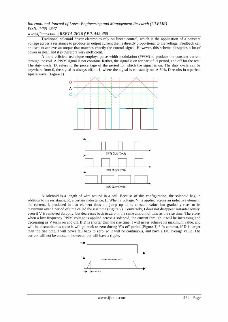
Traditional solenoid driver electronics rely on linear control, which is the application of a constant
voltage across a resistance to produce an output current that is directly proportional to the voltage. Feedback can
be used to achieve an output that matches exactly the control signal. However, this scheme dissipates a lot of
power as heat, and it is therefore very inefficient.
A more efficient technique employs pulse width modulation (PWM) to produce the constant current
through the coil. A PWM signal is not constant. Rather, the signal is on for part of its period, and off for the rest.
The duty cycle, D, refers to the percentage of the period for which the signal is on. The duty cycle can be
anywhere from 0, the signal is always off, to 1, where the signal is constantly on. A 50% D results in a perfect
square wave. (Figure 1)
A solenoid is a length of wire wound in a coil. Because of this configuration, the solenoid has, in
addition to its resistance, R, a certain inductance, L. When a voltage, V, is applied across an inductive element,
the current, I, produced in that element does not jump up to its constant value, but gradually rises to its
maximum over a period of time called the rise time (Figure 2). Conversely, I does not disappear instantaneously,
even if V is removed abruptly, but decreases back to zero in the same amount of time as the rise time. Therefore,
when a low frequency PWM voltage is applied across a solenoid, the current through it will be increasing and
decreasing as V turns on and off. If D is shorter than the rise time, I will never achieve its maximum value, and
will be discontinuous since it will go back to zero during V’s off period (Figure 3).* In contrast, if D is larger
than the rise time, I will never fall back to zero, so it will be continuous, and have a DC average value. The
current will not be constant, however, but will have a ripple.
International Journal of Latest Engineering and Management Research (IJLEMR)
ISSN: 2455-4847
www.ijlemr.com || REETA-2K16 ǁ PP. 442-458
www.ijlemr.com 453 | Page
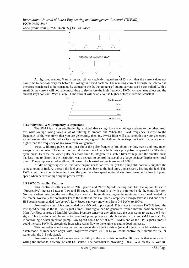
At high frequencies, V turns on and off very quickly, regardless of D, such that the current does not
have time to decrease very far before the voltage is turned back on. The resulting current through the solenoid is
therefore considered to be constant. By adjusting the D, the amount of output current can be controlled. With a
small D, the current will not have much time to rise before the high frequency PWM voltage takes effect and the
current stays constant. With a large D, the current will be able to rise higher before it becomes constant.
3.4.2 Why the PWM Frequency is Important:
The PWM is a large amplitude digital signal that swings from one voltage extreme to the other. And,
this wide voltage swing takes a lot of filtering to smooth out. When the PWM frequency is close to the
frequency of the waveform that you are generating, then any PWM filter will also smooth out your generated
waveform and drastically reduce its amplitude. So, a good rule of thumb is to keep the PWM frequency much
higher than the frequency of any waveform you generate.
Finally, filtering pulses is not just about the pulse frequency but about the duty cycle and how much
energy is in the pulse. The same filter will do better on a low or high duty cycle pulse compared to a 50% duty
cycle pulse. Because the wider pulse has more time to integrate to a stable filter voltage and the smaller pulse
has less time to disturb it the inspiration was a request to control the speed of a large positive displacement fuel
pump. The pump was sized to allow full power of a boosted engine in excess of 600 Hp.
At idle or highway cruise, this same engine needs far less fuel yet the pump still normally supplies the
same amount of fuel. As a result the fuel gets recycled back to the fuel tank, unnecessarily heating the fuel. This
PWM controller circuit is intended to run the pump at a low speed setting during low power and allow full pump
speed when needed at high engine power levels.
3.5 PWM Controller Features:
This controller offers a basic ―Hi Speed‖ and ―Low Speed‖ setting and has the option to use a
―Progressive‖ increase between Low and Hi speed. Low Speed is set with a trim pot inside the controller box.
Normally when installing the controller, this speed will be set depending on the minimum speed/load needed for
the motor. Normally the controller keeps the motor at this Lo Speed except when Progressive is used and when
Hi Speed is commanded (see below). Low Speed can vary anywhere from 0% PWM to 100%.
Progressive control is commanded by a 0-5 volt input signal. This starts to increase PWM% from the
low speed setting as the 0-5 volt signal climbs. This signal can be generated from a throttle position sensor, a
Mass Air Flow sensor, a Manifold Absolute Pressure sensor or any other way the user wants to create a 0-5 volt
signal. This function could be set to increase fuel pump power as turbo boost starts to climb (MAP sensor). Or,
if controlling a water injection pump, Low Speed could be set at zero PWM% and as the TPS signal climbs it
could increase PWM%, effectively increasing water flow to the engine as engine load increases.
This controller could even be used as a secondary injector driver (several injectors could be driven in a
batch mode, hi impedance only), with Progressive control (0-100%) you could control their output for fuel or
water with the 0-5 volt signal.
Progressive control adds enormous flexibility to the use of this controller. Hi Speed is that same as hard
wiring the motor to a steady 12 volt DC source. The controller is providing 100% PWM, steady 12 volt DC
International Journal of Latest Engineering and Management Research (IJLEMR)
ISSN: 2455-4847
www.ijlemr.com || REETA-2K16 ǁ PP. 442-458
www.ijlemr.com 454 | Page
power. Hi Speed is selected three different ways on this controller: 1) Hi Speed is automatically selected for
about one second when power goes on. This gives the motor full torque at the start. If needed this time can be
increased ( the value of C1 would need to be increased). 2) High Speed can also be selected by applying 12 volts
to the High Speed signal wire. This gives Hi Speed regardless of the Progressive signal.
3.5.1 Sinusoidal Pulse Width Modulation
In many industrial applications, Sinusoidal Pulse Width Modulation (SPWM), also called Sine coded
Pulse Width Modulation, is used to control the inverter output voltage. SPWM maintains good performance of
the drive in the entire range of operation between zero and 78 percent of the value that would be reached by
square-wave operation. If the modulation index exceeds this value, linear relationship between modulation index
and output voltage is not maintained and the over-modulation methods are required.
3.5.2 Space Vector Pulse Width Modulation:
A different approach to SPWM is based on the space vector representation of voltages in the d, q plane.
The d, q components are found by Park transform, where the total power, as well as the impedance, remains
unchanged.
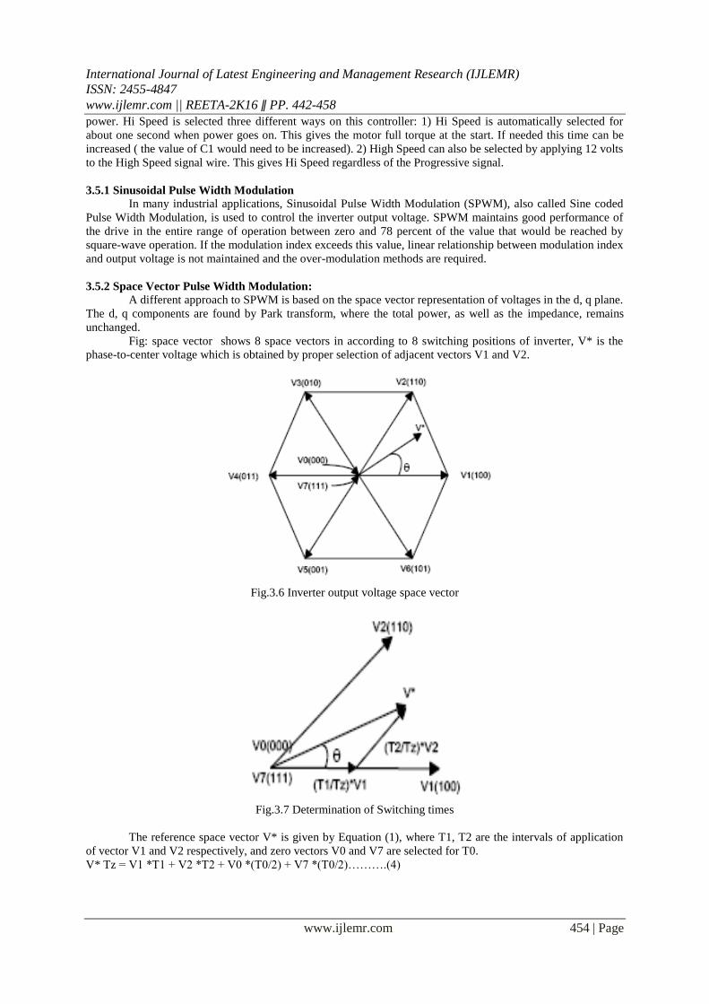
Fig: space vector shows 8 space vectors in according to 8 switching positions of inverter, V* is the
phase-to-center voltage which is obtained by proper selection of adjacent vectors V1 and V2.
Fig.3.6 Inverter output voltage space vector
Fig.3.7 Determination of Switching times
The reference space vector V* is given by Equation (1), where T1, T2 are the intervals of application
of vector V1 and V2 respectively, and zero vectors V0 and V7 are selected for T0.
V* Tz = V1 *T1 + V2 *T2 + V0 *(T0/2) + V7 *(T0/2)……….(4)
International Journal of Latest Engineering and Management Research (IJLEMR)
ISSN: 2455-4847
www.ijlemr.com || REETA-2K16 ǁ PP. 442-458
www.ijlemr.com 455 | Page
3.6 Modulation Techniques
Various modulation techniques may be adapted for the proposed topology. Carrier-based modulation
with sinusoidal or modified reference as well as non-carrier-based techniques such as space vector modulation
and selective harmonic elimination may be used to generate the gate signals. The choice of a modulation
technique is mostly a tradeoff among the requirements of the application, complexity of the software, and cost
of the control hardware.
3.6.1 Carrier-Based Modulation
Carrier set’s arrangement and reference waveform’s shape are the main sources of varieties in carrier-
based modulation techniques for multilevel inverters. As for carrier set’s arrangement, level shifted carriers LSC
and phase shifted carriers PSC are the two main categories that are respectively suitable for diode-clamped and
multi-cell structures. Two members in the LSC family, alternative phase opposition disposition APOD and
phase disposition PD are known to generate the best results for singe-phase and threephase applications,
respectively. PSC in its original form has been shown to generate a PWM waveform that matches with APOD.
Also a modified version of PSC with dynamic phase shift has been shown to match with PD.
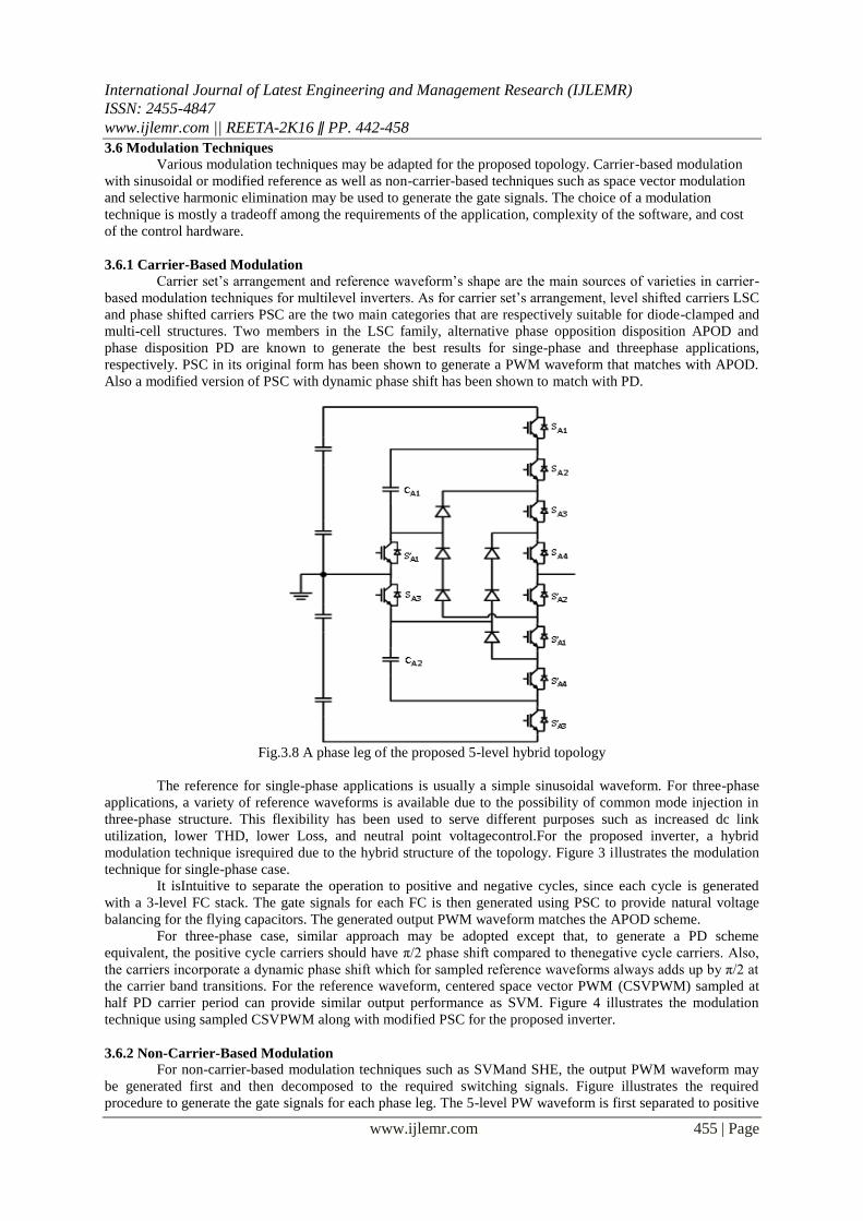
Fig.3.8 A phase leg of the proposed 5-level hybrid topology
The reference for single-phase applications is usually a simple sinusoidal waveform. For three-phase
applications, a variety of reference waveforms is available due to the possibility of common mode injection in
three-phase structure. This flexibility has been used to serve different purposes such as increased dc link
utilization, lower THD, lower Loss, and neutral point voltagecontrol.For the proposed inverter, a hybrid
modulation technique isrequired due to the hybrid structure of the topology. Figure 3 illustrates the modulation
technique for single-phase case.
It isIntuitive to separate the operation to positive and negative cycles, since each cycle is generated
with a 3-level FC stack. The gate signals for each FC is then generated using PSC to provide natural voltage
balancing for the flying capacitors. The generated output PWM waveform matches the APOD scheme.
For three-phase case, similar approach may be adopted except that, to generate a PD scheme
equivalent, the positive cycle carriers should have π/2 phase shift compared to thenegative cycle carriers. Also,
the carriers incorporate a dynamic phase shift which for sampled reference waveforms always adds up by π/2 at
the carrier band transitions. For the reference waveform, centered space vector PWM (CSVPWM) sampled at
half PD carrier period can provide similar output performance as SVM. Figure 4 illustrates the modulation
technique using sampled CSVPWM along with modified PSC for the proposed inverter.
3.6.2 Non-Carrier-Based Modulation
For non-carrier-based modulation techniques such as SVMand SHE, the output PWM waveform may
be generated first and then decomposed to the required switching signals. Figure illustrates the required
procedure to generate the gate signals for each phase leg. The 5-level PW waveform is first separated to positive
International Journal of Latest Engineering and Management Research (IJLEMR)
ISSN: 2455-4847
www.ijlemr.com || REETA-2K16 ǁ PP. 442-458
www.ijlemr.com 456 | Page
and negative cycle 3-level PWMs. Using state machine decoder, each cycle is then decomposed to two 2-level
PWMs i.e. the required gate signals for each FC cell.
It is important to note that this procedure is independent of the adopted modulation technique.
Therefore, it can be used with carrier-based modulation techniques as well as noncarrier-based. This might be a
good alternative when the complexity of the carrier-based technique is relatively high e.g. for PD scheme.
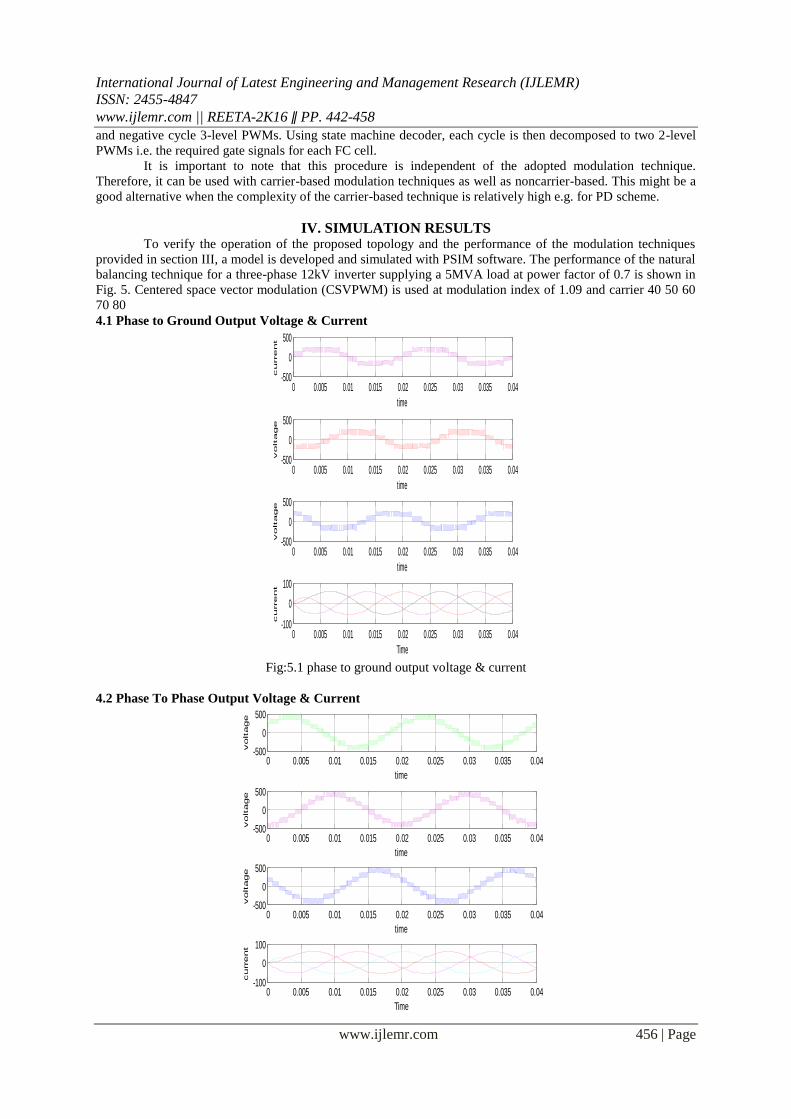
IV. SIMULATION RESULTS To verify the operation of the proposed topology and the performance of the modulation techniques
provided in section III, a model is developed and simulated with PSIM software. The performance of the natural
balancing technique for a three-phase 12kV inverter supplying a 5MVA load at power factor of 0.7 is shown in
Fig. 5. Centered space vector modulation (CSVPWM) is used at modulation index of 1.09 and carrier 40 50 60
70 80
4.1 Phase to Ground Output Voltage & Current
Fig:5.1 phase to ground output voltage & current
4.2 Phase To Phase Output Voltage & Current
0 0.005 0.01 0.015 0.02 0.025 0.03 0.035 0.04-500
0
500
time
current
0 0.005 0.01 0.015 0.02 0.025 0.03 0.035 0.04-500
0
500
time
voltage
0 0.005 0.01 0.015 0.02 0.025 0.03 0.035 0.04-500
0
500
time
voltage
0 0.005 0.01 0.015 0.02 0.025 0.03 0.035 0.04-100
0
100
Time
current
0 0.005 0.01 0.015 0.02 0.025 0.03 0.035 0.04-500
0
500
time
voltage
0 0.005 0.01 0.015 0.02 0.025 0.03 0.035 0.04-500
0
500
time
voltage
0 0.005 0.01 0.015 0.02 0.025 0.03 0.035 0.04-500
0
500
time
voltage
0 0.005 0.01 0.015 0.02 0.025 0.03 0.035 0.04-100
0
100
Time
current
International Journal of Latest Engineering and Management Research (IJLEMR)
ISSN: 2455-4847
www.ijlemr.com || REETA-2K16 ǁ PP. 442-458
www.ijlemr.com 457 | Page
Fig 4.2 phase to phase output voltage & current
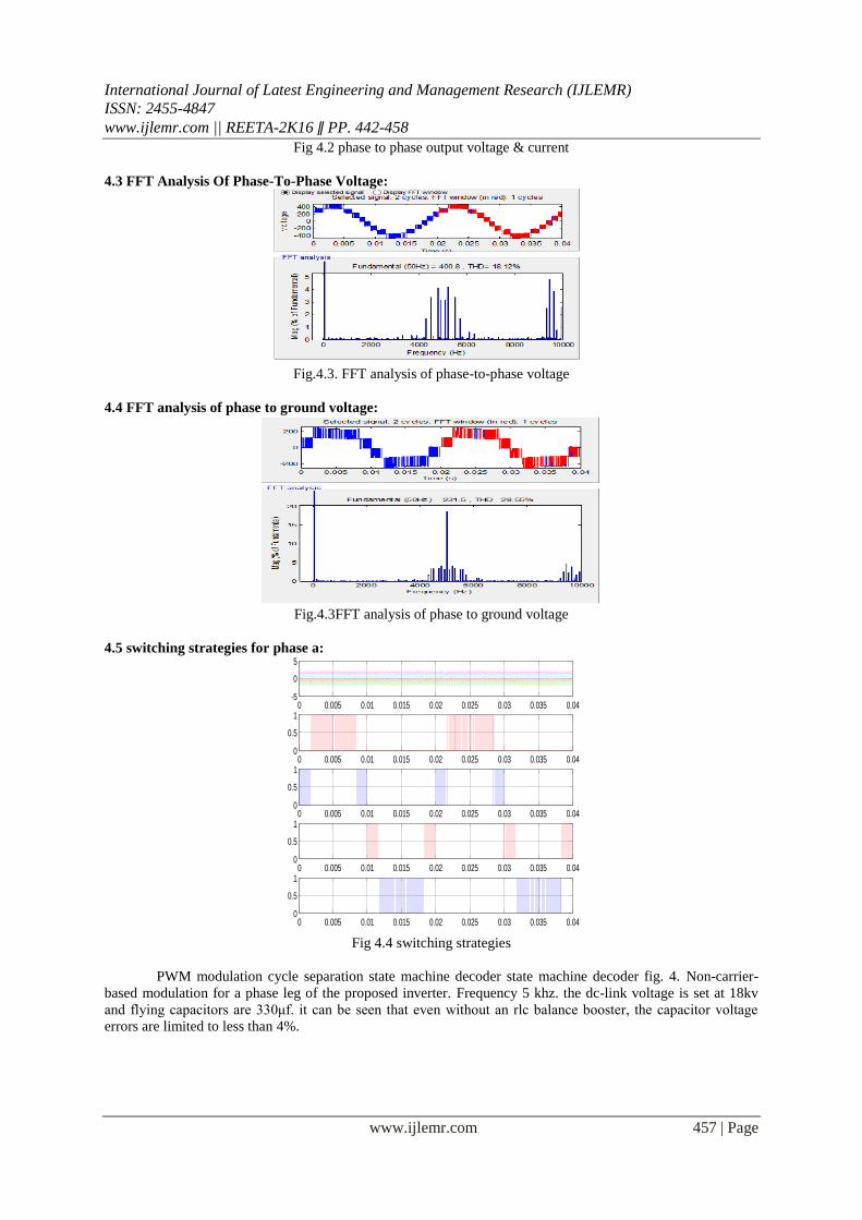
4.3 FFT Analysis Of Phase-To-Phase Voltage:
Fig.4.3. FFT analysis of phase-to-phase voltage
4.4 FFT analysis of phase to ground voltage:
Fig.4.3FFT analysis of phase to ground voltage
4.5 switching strategies for phase a:
Fig 4.4 switching strategies
PWM modulation cycle separation state machine decoder state machine decoder fig. 4. Non-carrier-
based modulation for a phase leg of the proposed inverter. Frequency 5 khz. the dc-link voltage is set at 18kv
and flying capacitors are 330μf. it can be seen that even without an rlc balance booster, the capacitor voltage
errors are limited to less than 4%.
0 0.005 0.01 0.015 0.02 0.025 0.03 0.035 0.04-5
0
5
0 0.005 0.01 0.015 0.02 0.025 0.03 0.035 0.040
0.5
1
0 0.005 0.01 0.015 0.02 0.025 0.03 0.035 0.040
0.5
1
0 0.005 0.01 0.015 0.02 0.025 0.03 0.035 0.040
0.5
1
0 0.005 0.01 0.015 0.02 0.025 0.03 0.035 0.040
0.5
1
Time
International Journal of Latest Engineering and Management Research (IJLEMR)
ISSN: 2455-4847
www.ijlemr.com || REETA-2K16 ǁ PP. 442-458
www.ijlemr.com 458 | Page
V. CONCLUSION a new hybrid 5-level inverter topology and modulation technique is proposed. Compared to 5-level
anpc as the most similar topology, this new topology requires two less switches at the cost of an additional
capacitor and six diodes.
However, since the capacitors still see the switching frequency and their size remain the same, it is
expected to reduce the inverter’s total cost. Also, unlike 5-level anpc, all switches must withstand the same
voltage which eliminates the need for series connection of switches and associated simultaneous turn on and off
problem. good loss distribution among switches can increase the inverters rated power or provide higher
switching frequency and smaller capacitor size.
VI. REFERENCES [1] h. abu-rub, j. holtz, and j. rodriguez, ―medium-voltage multilevel converters—state of the art,
challenges, and requirements in industrial applications,‖ ieee trans. ind.electron., vol. 57, no. 8, pp.
2581–2596, aug. 2010.
[2] s. kouro, m. malinowski, k. gopakumar, j. pou, l. g. franquelo, j. rodriguez, m. a. pérez, and j. i. leon,
―recent advances and industrial applications of multilevel converters,‖ ieee trans. ind.electron., vol. 57,
no. 8, pp. 2553–2580, aug. 2010.
[3] m. malinowski, k. gopakumar, j. rodriguez, and m. a. pérez, ―a survey on cascaded multilevel
inverters,‖ ieee trans. ind.electron., vol. 57, no. 7, pp. 2197–2206, jul. 2010.
[4] j. rodriguez, ―Multilevel inverters: a survey of topologies, controls, and applications,‖ IEEE Trans. Ind.
Electron., vol. 49, no. 4, pp. 724–738, Aug. 2002.
[5] J. Rodriguez, S. Bernet, P. K. Steimer, and I. E. Lizama, ―A Survey on Neutral-Point-Clamped
Inverters,‖ IEEE Trans. Ind. Electron., vol. 57, no. 7, pp. 2219–2230, Jul. 2010.
[6] J. Rodriguez, S. Bernet, B. Wu, J. O. Pontt, and S. Kouro, ―Multilevel Voltage-Source-Converter
Topologies for Industrial Medium-Voltage Drives,‖ IEEE Trans. Ind. Electron., vol. 54, no. 6, pp.
2930–2945, Dec. 2007.
[7] B. P. McGrath, T. Meynard, G. Gateau, and D. G. Holmes, ―Optimal Modulation of Flying Capacitor
and Stacked Multicell Converters Using a State Machine Decoder,‖ IEEE Trans. PowerElectron., vol.
22, no. 2, pp. 508–516, Mar. 2007.
[8] H. Sepahvand, M. Khazraei, K. Corzine, and M. Ferdowsi, ―Startup Procedure and Switching Loss
Reduction for a Single-Phase Flying Capacitor Active Rectifier,‖ Ind. Electron. IEEE Trans., vol. 60,
no. 9, pp. 3699–3710, May 2013.
[9] T. Bruckner, S. Bernet, and H. Guldner, ―The Active NPC Converter and Its Loss-Balancing Control,‖
IEEE Trans. Ind.Electron., vol. 52, no. 3, pp. 855–868, Jun. 2005.
[10] M. Narimani, B. Wu, Z. Cheng, and N. Zargari, ―A New Nested Neutral Point Clamped (NNPC)
Converter for Medium-Voltage (MV) Power Conversion,‖ IEEE Trans. Power Electron., vol. 8993, no.
MV, pp. 1–1, 2014.
[11] S. R. Pulikanti and V. G. Agelidis, ―Hybrid Flying-Capacitor-Based Active-Neutral-Point-Clamped
Five-Level Converter Operated With SHE-PWM,‖ IEEE Trans. Ind. Electron., vol. 58, no. 10, pp.
4643– 4653, Oct. 2011.
[12] T. B. Soeiro and J. W. Kolar, ―The New High-Efficiency Hybrid Neutral-Point-Clamped Converter,‖
IEEE Trans. Ind. Electron., vol. 60, no. 5, pp. 1919–1935, May 2013.
[13] F. Kieferndorf, M. Basler, L. a. Serpa, J.-H. Fabian, a. Coccia, and G. a. Scheuer, ―A new medium
voltage drive system based on ANPC-5L technology,‖ 2010 IEEE Int. Conf. Ind. Technol., pp. 643–
649, 2010.
[14] G. Gateau, T. A. Meynard, and H. Foch, ―Stacked multicell converter (SMC): properties and design,‖
in 2001 IEEE 32nd
Annual Power Electronics Specialists Conference (IEEE Cat.No.01CH37230), 2001,
vol. 3, pp. 1583–1588.
[15] T. A. Meynard, H. Foch, F. Forest, C. Turpin, F. Richardeau, L. Delmas, G. Gateau, and E. Lefeuvre,
―Multicell converters: derived topologies,‖ IEEE Trans. Ind. Electron., vol. 49, no. 5, pp. 978–987,
Oct. 2002.
[16] R.Naderi and A.Rahmati, ―Phase-Shifted Carrier PWM Technique for General Cascaded Inverters,‖
IEEE Trans. Power Electron., vol. 23, no. 3, pp. 1257–1269, May 2008.


![A Boost Type Nine-Level Switched Capacitor Inverterkresttechnology.com/krest-academic-projects/krest-mtech-projects/E… · cascaded H-bridge (CHB) [6]-[8], neutral point clamped](https://static.fdocuments.in/doc/165x107/5f4b8b46cfec67592c2cce41/a-boost-type-nine-level-switched-capacitor-inv-cascaded-h-bridge-chb-6-8.jpg)
