Boot Issues Processor comparison TigerSHARC multi-processor ...

University of Bath
PHD
A multi-family multi-processor education and development system.
Whitworth, P. F.
Award date:1983
Awarding institution:University of Bath
Link to publication
Alternative formatsIf you require this document in an alternative format, please contact:[email protected]
Copyright of this thesis rests with the author. Access is subject to the above licence, if given. If no licence is specified above,original content in this thesis is licensed under the terms of the Creative Commons Attribution-NonCommercial 4.0International (CC BY-NC-ND 4.0) Licence (https://creativecommons.org/licenses/by-nc-nd/4.0/). Any third-party copyrightmaterial present remains the property of its respective owner(s) and is licensed under its existing terms.
Take down policyIf you consider content within Bath's Research Portal to be in breach of UK law, please contact: [email protected] with the details.Your claim will be investigated and, where appropriate, the item will be removed from public view as soon as possible.
Download date: 07. Apr. 2022


A MULTI-FAMILY MULTI-MICROPROCESSOR EDUCATION
AND DEVELOPMENT SYSTEM
submitted by P. F. Whitworth
for the degree of Ph. D
of the University of Bath
1983
COPYRIGHT
Attention is drawn to the fact that copyright of this thesis rests with its
author. This copy of the thesis has been supplied on condition that anyone who
consults it is understood to recognise that its copyright rests with its
author and that no quotation from the thesis and no information derived from
it may be published without the prior written consent of the author.
This thesis may not be consulted, photocopied or lent to other libraries
without the permission of the author for four years from the date of
acceptance of the thesis.

ProQuest Number: U641726
All rights reserved
INFORMATION TO ALL USERS The quality of this reproduction is dependent upon the quality of the copy submitted.
In the unlikely event that the author did not send a complete manuscript and there are missing pages, these will be noted. Also, if material had to be removed,
a note will indicate the deletion.
uest.
ProQuest U641726
Published by ProQuest LLC(2015). Copyright of the Dissertation is held by the Author.
All rights reserved.This work is protected against unauthorized copying under Title 17, United States Code.
Microform Edition ® ProQuest LLC.
ProQuest LLC 789 East Eisenhower Parkway
P.O. Box 1346 Ann Arbor, Ml 48106-1346
To
Jim. my Father
Joan, my Mother
and Margaret, my Wife

Contents
Summary ivAbbreviations v
Chapter 1 Introduction 1Chapter 2 Educational Requirements 5Chapter 3 Existing Systems 12Chapter 4 Bus Structures 30
4.1 The Zilog Z80 Microprocessor 354.2 The Motorola M6800 Microprocessor 374.3 The Intel 8085 Microprocessor 394.4 The Mos Technology 6502 Microprocessor 404.5 The National Semiconductor INS8060 414.6 The Texas 9900 Microprocessor 424.7 The Intel 8086 Microprocessor 454.8 The Zilog Z8000 Microprocessor 474.9 The Motorola M68000 Microprocessor 504.10 The Motorola M6809 Microprocessor 524.11 The Ferranti FIOOL Microprocessor 534.12 The VAX 11/780 574.13 Bus Structures I Summary 61
Chapter 5 The Memory McUiager 655.1 Introduction 655.2 Fixed Window Memory Manager 665.3 Single Window Memory Manager 665.4 Multi-window Memory Manager 685.5 Integrated Host/Slave Memory Management 685.6 Variable Page Size Memory Management 69
i
Chapter
Chapter
5.7 The New Memory Management Scheme 705.8 Memory Manager Specification 755.9 Memory Manager Initialization 785.10 Provision for Direct Memory Access 806 Hardware Description 836.1 System Layout Considerations 836.2 The Processor 856.3 The Visual Display Unit 88
6.4 Input/Output 916.5 Board 1: Miscellaneous Functions 936.6 Read Only Memory 956.7 Random Access Memory 986.8 The Memory Management Unit 1016.9 Board 2: Miscellaneous Functions 1046.10 ,The 'Softy* Board 1096.10.1 Facilities 1116.10.2 The Softy Processor 1126.10.3 The Random Access Memory Buffer 1156.10.4 The Softy Display 1166.10.5 EPROM Programming 1196.10.6 Softy Modifications 1207 Master/Slave Interfacing 1288 The Target Microcomputers 1358.1 Specification 1358.2 The M6800 CPU Board 1368.3 The M6800 Interface 1428.3.1 Wait State Generation 1458.3.2 Bus Avallability Detection 149

Chapter
8.3.38.3.48.48.58.6
8.78 . 8
8.98.10
99.19.29.39.49.59.6
Chapter 10 11
12
131415
Control Signal GenerationM6800 Static ControlThe Motorola M68000The Motorola M68000 InterfaceThe Intel 8086The Intel 8086 InterfaceThe Ferranti FIOOLThe Zilog Z8000SummarySupport Peripherals Floppy Disk Interface Prestel Interface High Resolution Graphics Audio Spectrum Analyser «Other System Peripherals Summary Conclusions References Bibliography Acknowledgements Appendices Tables and Figures
151153155161168174178179180 183 183 188 189191192194195 199 202
218219220
III
SUMMARY
The rapid development of the microprocessor has not been matched by
the development of equipment to assist in the education of those who must use
the devices. As a result several different methods, based upon equipment
designed for other tasks, have become predominant.
This dissertation examines each of the commonly employed approaches and
compares their advantages and disadvantages. From this examination, a
specification for a system designed primarily to support microprocessor users
through both the stages of their own development, and those of the equipment
they design. The implementation of a system based upon this specification (the
main feature of which is the use of several microprocessors to assist the
user) is shown for several common microprocessor families.
The thesis contains both an appraisal of the future viability of the
concept and a bibliography of recent papers in the field of microprocessor
education.
iv
Abbreviations
This section lists the principal abbreviations used. Others (such
as the names of signals) are given on their first occurence In the text.
CPU Central Processing UnitDirect Memory Access
ECL Emitter Coupled LogicEPROM Eraseable Programmable Read Only MemoryIC Integrated CircuitIQ Input/OutputLED Light Emitting DiodeLSI Large Scale IntegrationLSTTL Low Power Schottky Transistor Transistor LogicRAM Random Access MemoryROM Read Only MemoryTTL Transistor Transistor LogicVDU Visual Display Unit

1. Introduction
The field of e lectronics Is widely regarded as being the fastest moving
of the many facets of human endeavour. It Is also generally accepted that the
fastest developing a rea within the field of e lectronics Is that associated
with the development of the Integrated circuit computer: the microprocessor.
The explosive growth of this field dates from 1971 with the introduction
of the '4004 ' by the Intel Corporation^ . This device was an attempt to design
the once and for a l l ' ca lcu la to r chip . Until this tim e, each new facility
provided for a calculator required a total redesign of the Integrated circuits
that gave the calcu lator Its properties. The idea that Intel Implemented in
the 4004 was that, if the basic capabilities required for any calculator were
available In a machine so that they couid be executed in any desired sequence
by p lac ing th e ir iden tif ie r in a list, the fac ili t ies provided by the
caicuiator could be radically altered merely by changing the list.
This is, of course, the principle of the stored program computer which
was already a proven and established tool. The difference was in the number of
Integrated circuits required to Implement an entire machine. This difference
Influences size and price, in the event, Buslcom, the Japanese company that
commissioned Intel to design the caicuiator IC went bankrupt, leaving Intel to
discover the ready market that appeared for the new device.
In the In te rven ing years , the power of the devices produced has
Increased, to such an extent that the latest microprocessor devices deliver
power com parable with that of m ainframe computers of the mid 1960's . In
conjunction with the Increased power of the processors has come a similar
Increase In the power of the support chips. For example memory chips hold many
times the Information and can retrieve It faster, whilst using less power and
sp a ce . In p u t /O u tp u t dev ices , o r ig ina lly confined to the ro le of
voltage /current translators, are now highly Intelligent In their own right and
1
provide significant support for the processor.
The race shows no sign of siowing and whilst this leads to enormous leaps
In technological achievement. It has also introduced major problems for those
who must learn, or educate people In these topics. Similar problems occur when
people who have finished their formal education have to develop, test and
support electronic systems based upon Increasingly more recent, powerful,
complex and cost effective Integrated circuits.
The aim of this work Is to c r it ica l ly exam ine the curren tly used
techniques, and in the light of results obtained from this examination, devise
a possible new solution to the problems.
Before any m icroprocessor based unit can be put Into full production
(which Is assumed to be the ultimate goal of any programme of education and
application) , there are several distinct phases of development that must be
passed through, not all of which are electronic development stages. The stages
can broadly be classified as a générai awareness of the avaiiable technology
and the application of that technology to a particular task.
Each engineer who works on microprocessor based equipment has to go
through a learning process to enable him to develop the skills necessary to
successfully design, build and debug a microprocessor based system. Some
skills will be an extension of o lder e lec tron ic skills whilst others will be
totally new. The learning process may have occurred within the context of a
University/Polytechnic degree course In electronic engineering or computer
science, or it may have taken place after this structured, formal phase of
education has finished and would then be by a refresher' or 'up-date ' course,
or by self education . It Is probable that not all ava ilab le devices will have
been covered, or all possible approaches to problem solution examined. Even if
the course had covered every currentiy avaiiable device, new versions, or
completely new devices, will have appeared In the Interval between the end of
2
the course and the time that the knowledge will be applied. It follows that
the engineer will have to up-date his knowledge at regular Intervals.
The com pany, as a corpora te entity, must also obtain knowledge of
microprocessor techniques. The knowledge required ranges from the difficulty
of Identifying programmed read only memories that are held In company stores
( th e re may be four or five different programmed versions, with no obvious
differences between the integrated circuits) through the problem of how to
deplct/specify a computer program (with the Inevitable revisions) for drawing
office purposes, to a general awareness of the strengths and weaknesses of a
microcomputer based product which can be tested electrically long before the
product Is specified, yet can never be proved 100% working at any time. The
Information required for company purposes varies In accordance with the task
of the individual concerned and really amounts to an awareness campaign. Once
this stage has been passed the appropriate practices will become normal
company policy and will survive the Inevitable changes of personnel.
At som e la te r stage the e n g in e e r will have to exam ine a range of
microprocessors w/f/» a part icular application In m/nd. This will take place
when the company Is developing its first microprocessor based product or when
the processor in use until then has proved Incapable of the new task or has
become obsolete. Usually organizational pressures will force the adoption of
one m icroprocessor for as long as possible as the reduction In research
equipm ent, company expertise, stock levels and field service replacement
stocks are some of the major attractions of a microprocessor based system. The
fact that a given application Is to be Implemented will seriously affect the
relative desirability of the different microprocessors.
The final stage of development Is that associated with the production of
a working, testable hardware/software combination that performs the required
functions. This phase will occur at least once for each project undertaken and
3
may represent a time period of several man weeks to many man years. This phase
is likely to be the only one which rece ives serious attention in terms of
budget allocation.
Each of the above mentioned stages represents a problem of education
associated with the same techniques and topic, yet the demands, problems and
finance available at each stage differ radically. The net effect Is that each
of the phases has forced the production of a d iffe ren t solution and no
coherent approach that enables the entire spectrum of microprocessor related
education to be taught with continuous support from one tool has emerged.
The other major use of microcomputers has been the provision of desk-top
computing facilities which concentrate entirely on the teaching, production
and use of software and programming techniques. Such facilities are desirable
because they are cheap, available on demand and are under the direct control
of the user. In terms of software education, the problems encountered with
microprocessor based equipment are not significantly different from those that
have been met with teaching based upon minicomputers or mainframe computers.
In each case the a rch itec tu re of the m ach ine Is hidden behind a wall of
standard programming languages (ALGOL. FORTRAN. 0 . PASCAL. BASIC) and operating
systems ( UNIX, C P / M ) . It Is therefore possible for a user to be unaware as to
the type of machine he Is using.
So, whilst It Is des irab le that any unit used as part of these genera l
education and development stages, lends Itself to the teaching of software,
this problem Is a lot less severe. Most of the discussions will centre on the
teaching of hardware on the assumption that any unit capable of this task wiil
be capable of use as a system software teaching aid.

2. Educational Requirements
The requirem ents at each level of development differ widely. At the first
stage, when the student Initially encounters the many concepts Involved In
microprocessor topics, any practical work should be designed to assist In the
assim ilation of these concepts. Exercises at this stage should be highly
structured and supportive and the student should be led towards the correct
understanding of a particuiar concept by attaining a sequence of intermediate
goals, with each successful completion Indicating the way forward. The concept
of selective fa i lu re ' Is significant. The student should not be thwarted In
pursuit of a goal by an Incorrect application of manipulative tools, yet must
not be allowed to attain a goal by the Incorrect application of a concept. An
obvious example Is the use of program execution commands where the letter E'
Is frequently used alone to Indicate that the program should start from Its
current state, whilst 'E1000' would Indicate that the program at location 1000
should be started. As all these addresses are In hexadecimal, 'EE' Is valid
but Is usually obtained as a consequence of miskeying, rather than a desire to
run w hatever program might start at location E'. It Is Inevitable that the
program residing at E' will destroy the recent programming efforts of the
student. Again, a paradox becomes apparent when the student must learn about
the correct use of manipulative commands since they are necessary parts of any
com puter sys tem , yet, until the concepts are completely understood, the
objects being manipulated, and thus the tools, are meaningless.
Resolution of this paradox can be achieved if the tools are automatic in
operation. In a sense, all computing related topics must be computer assisted.
The major points of Interest within a computer system are usually the values
of the Internal processor registers, the states of the Input/output devices
and memory locations currently holding program, data variables and stack data.
C o rrec t d isp lay of these e lem ents will Indicate such things as Interrupt
5
status and subroutine nesting depth. Access to these locations is usually by
register, input/Output and memory examination commands but experience shows
that such commands interfere greatly with the learning process by requiring
the use of sequences, whose logic is not yet understood. This difficulty Is
compounded by the excessive demands of finding the appropriate letters on the
keyboard at this very early s tage . The provision of autom atic display
facilities leads to an Important benefit. Just as chess playing computers can
be excellent tutors by demonstrating the wide choice of moves available, so
the student of microprocessors benefits from a display system that Indicates
all the side-effects of an action rather than leaving the student to examine
only the effects expected . A nother cruc ia l fea tu re requ ired of display
facilities is data translation s ince , at this s tage, the student will not be
capable of the automatic recognition of number patterns as being machine code,
text, data, stack data or meaningless rubbish. It is important that the data
be offered in as many forms as possible In order that such recognition can be
achieved.
Any hardw are assoc ia ted with a practica l investigation of topics In
m icroprocessing should a p p e a r sim ple at the level at which It is being
examined. Printed circuit boards should contain as few components as possible,
consistent with providing a machine capable of useful work, preferably one of
each type of device needed. The Immediate location and recognition of the
components discussed In lectures will assist In making the equipment less
mysterious. If the boards are overly large and com plex, they will not be
Identified with the simpler systems met theoretically. Of course, providing
the boards appear simple, the circuit can be as complex as required. This can
be achieved either by the use of programmable devices In place of larger
quantities of non-program m able parts, or by the removal of any additional
circuitry onto additional concealed cards.
6

The fina l req u irem en t of the in it ia l co n tac t stage Is an ability to
demonstrate which features are constant over several microprocessor families
and which are apt to change. If this Is to be successfully ach ieved , the
removal of Incidental changes Is of the utmost Importance. For example. If the
student Is told to exam ine two m ic ro c o m p u te r systems by d iffe ren t
manufacturers which use different keyboard commands to examine memory
(p e rh a p s E (x a m in e ) and M (e m o ry ) ) , this will be the f irs t d iffe rence
encountered and will tend to obscure the essential differences such as numbers
of registers and addressing modes.
After the concepts are thoroughly understood, the student Is likely to
encounter other m icroprocessor fam ilies . Each of these fam ilies will be
compared and contrasted with those already encountered to determine their
relative strengths and weaknesses. At this stage, the ability to examine the
devices using a common set of manipulative tools will be the most Important
feature of any practical work. The previously des irab le , highly supportive
system will now be required to allow the in te ll igent short cuts that reduce
the tim e taken to quantify the new device and Its support family. Display
fac i l i t ies will be requ ired to reduce the In fo rm ation presented to more
compact forms to allow more rapid examination of the data. Typlcaiiy, data
wlii oniy be required In Instruction form (w here applicable) and hexadecimal
form if data Is being displayed.
P ractica l work Is likely to con cen tra te on the areas of Instruction set
and hardware details In which the processor appears to differ from those
previously encountered. As students will have examined processors In different
orders . It Is Impossible to say which part icu la r details will strike them as
diffe ren t. At this s tage , not all the Im p lica tion s of each fea ture will be
m eaningful, they will merely be novel. Because of this. It Is likely that not
all unexpected sIde-effects will be examined further but in practice there are
7

some side-effects that are never observed.
It Is only when a part icu la r app lication Is under consideration that a
full evaluation of several processors can be undertaken and this represents
the third developm ental stage. As soon as the constraints of a practical
problem are applied, several microprocessor families will be discarded on the
basis of know ledge gained during exam ination of that fam ily for update
p urpo ses . It is g e n e ra iiy at this s tage that the dangers of Introducing
students to only one processor family become apparent. Instead of checking on
ava ilab le dev ices to locate the most cost effective processor which can
support the product line for many years to come, students exposed to only one
processor will check whether that processor can cope. If that Is the case, the
processor will be used regardless of Its suitability. There are many cases
where companies have decided on a processor family not because of Its merits,
but b e c a u s e It was the only one to which the ir f irst m ic roprocessor
experienced en g in eer had been exposed, if the eng ineer Is fam iliar with
several fam ilies , he wiii not oniy be able to choose from a wider selection
in it ia l ly , but will a lso possess the ab ility to exam ine new devices for
su itab ili ty . Of p a rt ic u la r Im p ortan ce Is the ability to derive data d irect
from m anufacturers ' data sheets, a skill which Is very necessary but rarely
taught.
Once the choice has been narrowed to one or two particular devices (by
whatever m ethod) , the next requirem ent Is for a unit on which any crucial
points of understanding can be Investigated. Prior analysis of the problem Is
like ly to p ro d u ce severa l con stra in ts that will be d iff icu lt to satisfy,
e ith e r In te rm s of timing or rep ea ta b il ity . Unless the en g in e e r Is highly
skilled, proof of the correct operation will be required by demonstration,
rather than calculation. This Is most easily achieved If a working system Is
already available , preferably capable of demonstrating all the features and
8

facilities of the particular device, yet offering a good level of support. The
support will be requ ired as the e n g in e e r , a lthough com petent with
microprocessor concepts and Indeed other microprocessors, will not necessarily
have experience of the chosen dev lce (s ) . From the project viewpoint. It Is
also desirable that a working prototype system be demonstrated as soon as
possib le . This will en ab le an exam ination by those responsib le for
commissioning the unit and allow the changes of specification that usually
follow from a demonstration of a working product. This Implies that the unit
Is initially built using a family of p re -b u ilt and tested modules wherever
possible, so that only the software need be written at this stage. As software
is often the hardest part of the project to specify and produce (certainly the
most expensive part of the development), any aids are beneficial, particularly
if two competing processor families are being demonstrated, it Is therefore
des irab le that the software Is in itia lly written In a high level language,
even though severe time and memory size penalties will be Incurred. Compilers
can then be used to transfer the task to the appropriate machine code. Usually
the resultant system will be adequate for demonstration purposes and will
assist In tightening the specification before more time Is spent on production
software.
The ready availability of a wide range of p re -b u l lt modules will allow
for the correct positioning of the hardware/software trade off. it Is usually
true that tasks can be performed with simple hardware using complex software
or v ic e -v e rs a . As software Is expensive In d eve lo pm ent but cheap In
production, whilst hardware Is the reverse, the correct balance between the
two must be maintained. This Is even more difficult where there are several
mutually exclusive trade offs that can be manipulated. Such a case occurs If
the system performs several, related complex tasks.
As the time and memory size constraints will have been abandoned to allow
9

the use of high level languages, the prototype Is now likely to consist of a
pre-bullt modular hardware, a 'conceptual software system' that demonstrates
the major features of the system and a selection of the more crucial sections
of software and hardw are ava ilab le to prove the ability of the system to
perform the task at production level. It will now be possible to move forward
to the final development stage, where one family Is selected and a complete
integrated production hardware/software unit Is produced and debugged.
It Is usually at this stage that suffic ient f in an ce Is ava ilab le to m eet
all the requirements of a design engineer. A microcomputer will have to be
constructed that provides the required facilities, in terms of program space
and Input/output facilities, yet meets the constraints of power dissipation,
board size and production cost. This unit must be made functional, and there
are several techniques for achieving this. The simplest method is to use in -
clrcuit emulation. Here the processor, which by the nature of the system has
com plete control of all other devices. Is rep laced by a cab le leading to a
complete test micro or minicomputer. The microcomputer provides facilities for
exam ination of all reg is te rs , memory and Inpu t/ou tpu t locations and Is
designed so that programs can be executed even In the presence of memory
faults. This enabies the exercising of the system under test. The problems of
testing microcomputer systems are usually aggravated by the long time period
of any waveforms Involved. If the waveforms can be made simpler and more
repetitive, they are am enable to study by oscilloscope rather than the far
more expensive and complex logic analyzer. The simplest way of obtaining
repeatable waveforms is by the use of short test programs. The running of
these programs, which requires working memory/processor system. Is simplified
by memory simulation in the debug system. Software debugging Is likely to
revolve around the three facilities of single stepping the program so that a
section of code which does not work can be examined In detail, data snapshots
10
In which the values of se lec ted locations are au tom atica lly stored at
Intervals for later analysis and. finally, the ability to examine the sequence
of events that leads up to some abnormal condition of the system. This Is
usually done by a trace facility In which each bus cycle is captured In a high
speed memory, the capturing process stopping when the abnormal event is
reached. The above three facilities will usually be arranged to operate under
certain special conditions such as input/Output access only, instruction fetch
only, only between locations XXXX and YYYY or combinations of the above.
Given the above desiderata, the next chapter will examine the popularly
used techniques for providing microcomputer education and development and
discuss their respective strengths and weaknesses.
11
3. Existing Systems
In the field of m icroprocessor development systems and education, four
major classes of equipment have tended to predominate and the literature shows
support for each of the various methods or combinations thereof. In this
chapter, each of the common approaches will be discussed In terms of Its
suitability for use In the four developmental stages previously outlined. For
each of the approaches a reference to representative paper will be given.
Other relevant publications are listed In the bibliography, arranged according
to the type of system advocated or discussed. In fact, the vast bulk of papers
on microcomputer education over the past few years can be found In four Issues
. 2 , 3 , 4 , 5 of various Journals
When microprocessors were first Introduced, the manufacturers realised
that the radical d ifferences between discrete logic Implementation and a
microprocessor based implementation of a task would. In Itself, be a major
factor governing the a c c e p ta n c e of the new dev ices . This led to the
Introduction of eva luation cards which are usually single board
microcomputers. In the earliest models, a microprocessor would be supplied
with a monitor program located In read only memory, a very limited amount of
random access memory, one or two parallel Input/output devices and a serial
input/output device with a teletype interface. These cards were very difficult
to expand since they had been designed to be as cheap as possible consistent
with producing a demonstrable system. However It Is In the best Interests of
the manufacturers to provide a high level of hardware and software support for
their products and the preferred supportive tool Is usually a development
system produced by the m anufacturer with typical prices of three to eight
thousand pounds. Whilst such a sum Is a reasonab le cap ita l cost to be
amortized over a contract or product lifetime. It Is unreasonable as part of a
speculative development budget, where the low cost development cards are
12
widely used. The requirement for a teletype proved to be a limiting factor for
many companies with no previous computer usage, as the development cards were
In the region of one to three hundred pounds, whilst a teletype was three to
six hundred pounds. The later versions recognised that many users would not
possess terminals and so provided a hexadecimal keypad and display as an
alternative to the teletype. Storage of programs was achieved using the paper
tape reader/punch associated with the teletype or a domestic cassette recorder
and modem circuit. Support for the user was generally limited to commands to
examine registers and memory and alter them as required, Insertion and removal
of breakpoints '. In which the program runs as normal until the specified
location Is reached, and the provision of program single stepping.
There can be little doubt that these boards spurred the development of
the first hobbyist and home com puters . However until this m arket was
recognised, the microcomputer was seen primarily as an electronic circuit
replacement, rather than a cheap, small computer. In turn, the development of
the home computer led to the realization of the potential of the domestic
television as a cheap display device. The latest generation of single board
computers produced by the manufacturers have appeared In support of the new
generation of sixteen bit microprocessors and, due to the complexity and cost
of the processors they contain, some manufacturers have moved back to the
visual display unit as being the only practicable display method. For example,
the M otorola 68000 has sixteen, th irty-tw o bit reg isters to display and a
hexadecimal display Is not too convenient. Others, like the Intel 8086, have
retained the hexadecimal keyboard and display. This places them at a serious
disadvantage, s ince, with the Introduction of Improved architecture and
reduced cost of all types of memory. It Is now possible to offer such features
as mnemonic assembly and symbolic debug as cost effective facilities. Both
these facilities require that a full QWERTY keyboard and display be available.
13
in g e n e ra l, the m anufacturers differ as to the extent of expandability
made available to the purchaser of evaluation boards. Whilst most will allow
the addition of extra standard m emory or Input/ou tpu t dev ices. It Is not
uncommon for the more powerful control signals, such as Interrupts, slow
memory handshake etcetera, to be dedicated to providing facilities associated
with the simple user Interface that the units possess. Typically, the most
Important Interrupt will be reserved for program abort or single step, while
In many cases, full address decoding Is not performed, thereby saving the cost
of several Integrated circuits.
The hobby computers have developed to a stage where there are many single
board computers which are not produced by the manufacturers of a chip family
and which can thus combine the best products of several manufacturers. In the
main, the Independently produced boards have used the Zilog Z80 and the MOS
Technology (now owned by the largest Independent board m anufacturer.
Com m odore Business M achines) M CS6500 s e r ies , notably the 6502 .
These facilities show a much wider divergence than the boards produced by
m anufactu rers , largely because of the e lem ent of com petition . For the
m anufacturers, the single board computer Is a device to aid In the sale of
chip families; for the independent manufacturers. It Is the main business. It
Is th e re fo re possib le to buy single board com puters with a full QWERTY
keyboard, video Interface and one high level language ( usually BASIC) at a
price below that of the manufacturers' minimal system.
Sing le board com puters have frequently been used as the basis of a
microcomputer teaching laboratory and a typical laboratory based on such units6
Is described by Cahill, Laverty and McCokell . The major advantage presented
by the single board computers Is one of cost. A typical first year electrical
en g in e er in g Intake of fifty to one hundred students will requ ire a large
number of workpolnts If problems of timetabling are not to become acute. Ten
14

student positions can represent a large capital outlay. This leads to the
attraction of boards costing a few hundred pounds, but, of course, such
boards fall short of the Ideal arrangem ent. When used during the Initial
stage of development, the boards suffer from several disadvantages. Due to the
constraints Imposed by their low cost, the boards that employ hexadecimal
keyboards and displays cannot offer facilities such as editors and assemblers.
In add it ion . It Is likely that up to one third of the board a re a will be
associated with keyboard and display functions. Those cards using a VDU
in terface will have s im pler e lectron ics but now require the addition of a
visual display unit for each station with attendant costs, if such a board is
used with the vdu, it will be able to support editors and assemblers only by
Increasing the size of read only and random access memory held on the board.
This is due to the difference In size that exists between system software and
typical small control tasks. For example, on the Z80, a small assembler will
occupy about four kilobytes, a BASIC interpreter uses eight kilobytes, whilst
a malor control unit with a large number of embedded messages might also take
eight kilobytes. Contrast this to the average single chip microcomputer with,
at m ost, two kilobytes of read only m em ory or the typ ica l final year
university p ro ject software of severa l hundred bytes. If the system is
designed to cope with the dem ands of such supportive softw are . It wlli
inevitably be more complex. Further difficulties arise when the program must
be run. As any editor/assembler must be both memory resident and edit/assemble
from memory to memory (due to the lack of storage p e r ip h e ra ls ) , it wiii be
possible for the source code to be corrupted if the program is incorrect. This
will mean extra time spent correcting or re-entering the programs.
As the cards are the products of different manufacturers, command formats
will d iffe r , p resenting a serious handicap to the student at this stage.
Problems will arise for those responsible for producing and m aintaining
15

laboratories based on such units, if interfaces to equipment in the iaboratory
are required. This wili occur because of the diverse bus standards used by the
various manufacturers. For example. If a special laboratory Interface was
produced, the different bus timings . card and connector formats would
necessitate much duplication of effort as each m anufacturers card would
require Its own Interface to the equipment. Such boards are also Inadequate
for system software education tasks, s ince, as stated, system software Is
typically far larger than the software for embedded computer controllers. At
the up-date stage, which represents the market the cards are primarily aimed
at. the differences in monitor commands wiil now represent an annoyance rather
than a m ajor handicap which will reduce In significance even further If the
time Intervals between updates on different processors Is extended. As no
major tasks are attempted at this stage, limitations of monitor and hardware
will not prove to be too serious.
If a product prototype Is being d ev e lo p ed , the boards can form an
Invaluable starting point for the construction of dedicated hardware. The
provision of a processor card that Is known to be working provides the means
for running exercise programs to assist In the testing of other sections of
the hardware. As with the laboratory, there will be problems of Interfacing If
a company Intends to build prototypes based on more than one manufacturers'
product. The lack of support Is likely to prove the major problem. Any project
that req u ires more than a few lines of ass e m b le r code will suffer If an
assembler Is not used. Updating the software as errors are corrected, and
providing adequate program documentation and description for debugging
purposes become much more difficult. The use of an assembler requires an
editor to construct and co rrec t the Input text. At the full hardware and
software Integration level, the prototype cards cannot offer any assistance
other than an em ergency supply of spare Integrated circuits and test bed
16

facilities for suspect integrated circuits.
The independentiy manufactured single board computers offer better
facilities, but this is usuaiiy achieved by the use of a high levei language,
typically BASIC, and thus the true architecture of the processor Is hidden.
This renders the board less useful as a teach ing aid during the in itia l
concept stage. The use of a full QWERTY keyboard and television set or monitor
does Improve fac i l i t ies at low cos t, but this Is offset by the necessary
increase in board compiexity. At the up-date stage, the additional features,
being rarely directed to assembly language support, render the cards little
d iffe ren t to those supplied by the m an u fac tu re r . This Is also true at
prototype and full hardware/software Integration levels.
The use of multlboard self-contained microcomputers also receives much
support^. Such machines consist of a processor with large quantities of random
access memory and software either in read only memory or on disk. The earliest
systems were designed as hobbyist com puters and cheap m in icom puter
replacements. The major handicap for the eariiest units was the lack of fast,
non-volatlle back-up storage. It was not until an Intel employee, experimented
with the addition of a floppy disk drive (designed by IBM to replace punch
cards and paper tape as an original data entry m ed ium ). that the units could
begin to compete with their larger brethren. At this tim e, the most widely
used minicomputer was the POP 8 series and an operating system was written for
the Intel 8080 based on that used by DEC on the PDP-8. This was marketed as
CP/M and. because of the uniform programming environment provided for many
machines, software became available from many different sources. The uniform
programming envlroment was achieved by taking the lowest common denominator in
terms of hardware faciiities. but. as microprocessors have developed. CP/M has
been retained because of the large amount of software available. However,
compatablllty must be retained If C P /M Is to be useful and the changes made
17

are largely cosmetic. Several other companies developed products based upon
the MCS6502 microprocessor, notably the PET and the Apple. Both these units
were sold on the turnkey system approach, the user would not need to look
Inside the box. As no common 6502 operating system appeared, software had to
be written especia lly for each of these m ach in es , lim iting the quantity
available. One advantage enjoyed by the Apple over C P /M machines Is that It
possesses high resolution graphics as standard and Apple software writers were
not slow to cap ita lize on this for games and graphics packages. It Is an
Indication of the hold that C P /M has on the market that It Is now possible to
buy a plug-ln Z60 sub-system for both the PET and Apple to enable them to run
C P /M software.
More recently , using the latest generation sixteen bit processors, the
new generation of self-contained microcomputers can simultaneously support
several users, have in built twenty megabyte W inchester technology disk
drives, megabyte memories and rival many minicomputers. Whilst they can still
represent a cheap alternative to a minicomputer, the user does not have to
lose any computing power.
All the self-contained microcomputers were designed primarily for use as
software machines. Indeed, the most commonly used machines (Apples and SlOO
bus based) are both organized so that Interference with the bus by outside
devices for direct memory access purposes Is difficult. If not Impossible.
When used at the Initial concept stage, they can provide a good Insight Into
the software activities of a m icroprocessor and if provided with a range of
p r e -b u l l t In te rfaces they o ffe r a method of dem on stra t ing In te rfac ing
software.
Apart from their higher capital cost, more than one type of machine will
be needed If more than one processor Is to be studied. As the debugging
facilities for these machines tend to be more capable, the commands are more
18
numerous and complex and differences between the units will be a greater
barrier. In addition, the problems associated with supporting these machines
wili become more severe. Transferring programs between machines that store the
data in d ifferent fo rm a ts , and the use of d ifferent suppliers and service
agents all act to make this approach for te a c h in g labora to r ies less
attractive. At the up-date level, the units represent a large Investment that
Is unlikely to be recoupable , unless the devices are then used as general
purpose processors, when the objections mentioned above will appear. Prototype
work can make use of such machines as a basis for adequate project software
support, but the problem of Incompatible Input/output modules will again
occur, as , despite the attempts of the Institute of Electrical and Electronic
8Engineers , no Industry wide standard bus has emerged. Once again, the units
have no hardware support to offer at the hardware/software Integration stage.
The use of m a in fra m e /m in i-c o m p u te r s im ula tions Is the third major
approach taken to the problems of microcomputer education and development. In
such systems, a program runs on a mainframe and provides an editor and
assembler as well as simulating the action of a m icroprocessor system. The
description here is of the MicroSim package by D. M . England & Partners Ltd. The
user gains access to the computer as appropriate and using the normal commands
of the system, the relevant simulator for the m icroprocessor of Interest Is
executed. Once this occurs, the user Is In a standard environment that changes
little for all the computers the package Is available for. The environment
suffers from the requirem ent that the package be transportable to different
computers In that the terminal handler Is written In FORTRAN and only provides
line editing capability . Ail lines are prefixed with a num ber which Is used
for all ed it ing re ferences and , as with the BASIC lan g u a g e , the lines of
program will be executed In ascending line number order. Sections of program
are created as segments and, whilst references to other objects Is by simple
19
label, objects In other segments are referenced by composite labeis of the
form 'segmentname. iabeiname'. There are no assembly or link passes, so that,
as each line Is entered. It Is compressed to an Internal format based on the
appropriate machine code. A request for a listing will produce a standard list
format showing program counter, machine code, labels, source statements and
comments. It Is also possible to generate an output of machine code only,
suitable for transfer to a m icrocom puter. Input/output Is not available to
real devices, and Is e ither directed to the keyboard, w here data can be
entered In any base des ired , or to a subroutine, written In the relevant
assembler, which Is called for each byte to be transferred. This Is designed
so that the user can simulate input/output devices of any complexity. There Is
currently no capab ility for Input/ou tpu t to files on the m ain fram e which
limits the amount of processing that can be done on data gathered 'In the
f ie ld ' . An advantage of the simulator Is that. If the program attempts to
execute data or an Instruction that conflic ts with previously d ec la red
Instruction boundaries, the simulator will report an error. This Is a major
benefit when students are first Introduced to programming, as a very common
error Is to omit the program termination. As this feature can not be disabled,
the ability to alter code during execution Is not demonstrable, though some
might argue that this Is a positive constraint, rather than a negative one.
U nfortunate ly , th e re Is no program single step trace c ap ab il i ty , and
examination of the registers is somewhat awkward.9
Due to the popularity of the C P /M operating system, Gilbert at Surrey
University has s im ula ted not only a Z 80 , but also floppy disks and the
routines to drive them. This package, written in FORTRAN and called HORACE
( Horizon and CP/M Emulator) will run any CP/M program, and CP/M compatibility
is ensured in that the first program loaded Into the simulated Z80 Is C P /M
Itself. A major feature of HORACE Is that extremely powerful debug facilities
20

are provided. Whilst simple debug tasks can be requested easily, a debug
language exists which can be used to create new debug commands that offer
conditional execution, action on specific values of registers, or only between
limited addresses.
The simulators offer many advantages. Where the time sharing computer Is
already available, as many student positions as necessary can access the
simulator without difficulty. Due to the ability of the sim ulators to check
the legality of an Instruction before It Is executed, many Initial mistakes
are caught and reported rather than destroying the entered program. Where the
packages have been Implemented on several different processors, students can
simulate the same task on several machines, yet retain a common working
environment with stable manipulative tools. The simulator can provide useful
software support at all levels.
Theoretically, the most powerful approach to all phases of microprocessor
education and development, but also the most expensive. Is the use of In -
circuit emulation based development systems. Designed by the manufacturers to
be the preferred tool for prototype and full hardw are/softw are Integration,
they operate on the basis that, as the microprocessor controls the system,
control of the microprocessor provides all the necessary access to the system.
To provide the ap p ro p r ia te d e g re e of co n tro l , a m ic ro p ro cess o r 1C Is
surrounded by auxiliary circuitry and placed In a pod' which Is connected to
the host development system by a multiway cable and to the system under
development by an Integrated circuit header which has the same pIn-out as the
microprocessor. In use, the microprocessor Integrated circuit Is removed from
the board to be debugged or examined and Is replaced by the header. Now the
development system can, via the auxiliary circuitry, reset, halt or Interrupt
the m icroprocessor and force It to e ither use memory In the development
system, or that In the system under test. In a similar fashion, the memory and
21

in p u t/o u tp u t devices of the system under test can be accessed by the
development system simulating the action of a processor executing a program
that requires such an access. This process is shown diagrammatlcally In Figure
3 .1 . Now, using the software support facilities of the development system, the
user can develop and assemble programs Into a form that can be loaded Into
memory. In the first Instance, these programs will usually reside In random
access memory provided by the development system, even though they might
eventually be placed In read only memory In the system under test. As there Is
a microprocessor of the relevant type In the In -c lrc u lt emulator pod, the
programs can be executed before any hardware has been built, providing that
they do not attempt to perform too much Input/output. As the development
system will usually provide sophisticated breakpoint facilities, all routines
that call for Input/output can be breakpolnted so that the user may deposit
values Into the appropriate registers from the development system keyboard. In
this way, many sections of the program can be debugged In advance of hardware
availability. It has already been stated that microprocessor based hardware
can best be debugged by the use of small test programs that exercise' the
hardware so that faults can be traced easily with conventional tools. As soon
as a hardware system has been attached to the emulation pod, the development
system user can specify that an access to a particular location In the memory
should be serviced by either the development system memory, or that of the
system under test. This assigning of responsib ility cannot be done for
Individual locations, but rather for groups of, typically, 256 locations at a
time. The user can. therefore, leave a program in random access memory In the
development system, rather than transferring It to read only memory In the
system under test (with the attendant difficulty of changing the program each
time an error Is lo c a te d ) , yet use memory and Input/output devices In the
system under test where possible and desirable. If the memory and Input/output
22
devices will not work, a program can run In the development system that tries
to access locations in the system under test, allowing the user to test logic
states with any desired tool or the limited logic analyzer capability that Is
often provided by the development systems In conjuntlon with the program trace
cap ab ility , if this Is d o n e , the user will a ttach test leads to a se lected
number of points and run the test program. Then, for each bus cycle generated
by the test p rogram , a display will be generated that shows the value of the
microprocessor data, control and address buses as well as that of the selected
test points. A comparison can then be made between expected and obtained
results, and the problem area can be restricted until rectification becomes
possible. It is usual for any development system of this kind to provide EPROM
programming capability, so that once programs have been tested they may be
transferred to perm anent residence In the system under test. If, at some
future date , a fault In either hardware or software becomes apparent, the
microprocessor can be removed and replaced by the emulator and critical
locations examined or changed, and program execution traced. This is extremely
convenient as It removes the necessity of providing term inal support and
program m onitoring software within the unit. This Is d es irab le for, as
mentioned previously. In embedded computer systems, system software Is usually
far larger than the task software.
The developm ent systems d escrib ed fa ll Into two c lasses ; the
microprocessor manufacturer supplied, and those produced by Independent
com panies. Those associated with a m anufacturer, for example the Intel
Intellec, Motorola Exorciser, National Starplex, could originally only support
one processor. As the product families grew, the need to support more than one
family on one machine became apparent. Now the above units support most of the
named manufacturers products, if not with hardware emulation, at least with
software development. The units produced by the Independents are more
23

expensive , typ ically eight to ten thousand pounds com pared with a
manufacturer's version at five to eight thousand, but have the advantage of
offering support for more than one manufacturers' products. These are the
'universai' microprocessor development systems or UMDS's. In particular, there
are th ree m ajor suppliers of universal developm ent systems, Tektronix,
Hewlett-Packard and Millennium Microsystems. Again, the range of facilities
varies according to price, some systems offering hexadecimal keyboards and
memory examination only, whilst others that are disk based offer complete and
capable software development facilities.
Whilst the In -c lrcu lt emulators offer the most powerful approach to the
problem of microcomputer education, there are three probiems that must be
overcome. The first major barrier to greater use is that of price. Systems
that typically cost from five to fifteen thousand pounds per station, and will
only offer em ulation of one processor for that p r ic e , are accep tab le In
commercial development project terms, but not at any of the other development
stages. The price of these systems Is partly due to their great complexity,
and could only be reduced If the complexity were to fall. The second problem
Is that the systems do not provide a m inim al m ic ro processor board for
e x p e r im e n ta l /e d u c a t io n a l use. The fina l problem asso c ia ted with the
development systems Is that to date, all have been sold as a complete package.
This has tied the user to the only source of software, the development system
manufacturer. The software supplied Is obviously written with the competent,
fu ll - t im e user of the development system In mind since there Is very little
support at any level. As the opera ting systems are all p roprie tary , the
suppliers have not been Inc lined to supply details of the user software
Interface to the purchasers. This has Inevitably restricted the ability of the
user to write more software that suits their particular needs. With the above
lim itations, the use of In -c lrcu lt em ulators In education laboratories has
24
10been limited, one exception being at Beil Laboratories
One very important feature associated with the in-circuit emuiation based
systems is the use of one microprocessor, within the development system, to
assist In the examination of a target system. The power of this approach Is
further enhanced by the removal of all user supportive tools and complexity
from the system under Inspection. Whilst this Is at Its most extreme In the
In -c lrcu lt em ulators, where the m icroprocessor under Inspection is also
removed, the use of additional user supportive processors also appears In two
other methods, the timesharing mainframe connected to a target processor by a
serial link, and the dedicated m in i/m icrocom puter connected by a serial or
parallel link.
The use of two processors enables the com bining of the best facilities
presented by two different approaches. For example, the most common support
arrangement Is the provision of single board computers with a visual display
unit and a seria l link to a m in icom puter^ \ The student uses the visual
display unit to access the m in ico m p ute r and run the editors and cross
assemblers or simulators that will create his program. Once the program Is
prepared , the minicomputer enters It, via the three way switch, into the
microcomputer. The terminal then connects to the microcomputer and the student
uses a monitor resident In the m icrocom puter to examine and execute the
program which is now freed from the constraints of minicomputer simulators and
can use any Input/output facilities required. There are several advantages to
be gained by this approach. With the removal of the editors and assemblers
from the microcomputer to the minicomputer, the microcomputer system can
becom e s ign ifican tly s im pler. The user also benefits from the better
fac ilit ies that are ava ilab le with m in ico m p ute rs , such as s im ultaneous
printing of files during execution of other program s. However, there are
problems associated with this approach. The monitor program that resides
25

within the microprocessor must be in read oniy memory, and aithough it is
reduced in s ize, it wiii stiii be a compiex p iece of software that must be
written In the assembler language of that microprocessor. The monitor must be
present to aliow the user to examine and aiter memory locations and control
the execution of programs. The program can only be discarded If some other
agency then becomes responsible for these functions. This implies the removal
of software complexity by increasing the hardware complexity - an exampie of a
hardware/software trade off.
The In -c irc u l t em u la to r ach ieves this by the rep lacem e n t of the
m icroprocessor Integrated c ircu it by a debug unit. Another method Is to
provide an externally controlled direct memory access channel Into the system.
Direct memory access is the Input/output technique whereby the processor
Initializes a counter system that will provide an address at which Incoming
data Is to be stored, or outgoing data to be found. Thereafter, whenever the
Input/output device requests a transfer, the counter system will take control
of the processor bus, provide address and control signals appropriate to the
participating memory location and manipulate the signals necessary to achieve
a transfer to the Input/output device. Once a transfer has been completed, the
counter will Increment and be ready to repeat the process without further
processor Intervention. This reduces the workload on the processor and enables
the processor to undertake other work whilst also allowing a far higher peak
data tra n s fe r rate to be a c h iev ed . Obviously, if d ire c t mem ory access
in it ia liza t ion is passed to the in p u t /o u tp u t d e v ic e , ( in this c a s e , a
m in icom puter), the processor plays no part at all In such transfers and hence
no program Is required. An Implementation of such a system between a Digital
Equipment Corporation PDPl 1 / 2 0 minicomputer and a Motorola 6800 based12
microcomputer Is described by Holdstock . and to a Ferranti F100L based13
microcomputer by Selwyn . The use of a minicomputer has severai advantages.
26

As most minicomputer operating systems can support more than one user
simultaneously, one machine can support an entire laboratory. Users and those
responsible for software maintenance benefit from the well supported packages
( such as editors) that are supplied with such systems. Inevitably there are
disadvantages, particularly the fact that the minicomputer represents a large
capital cost that Is largely Independent of changes In the number of working
positions supported. Shouid the minicomputer fail, the entire system becomes
Inoperative until a repa ir is effected and it wili be impossibie to move the
system for prototype or demonstration purposes.
Another major disadvantage is the method that must be used to Implement
the controlled direct memory access channel Into the microcomputer. Typically,
high p e rfo rm an ce m u lt i -u s e r m in icom puters employ high speed, tight
specification processor buses which are maintained by the manufacturers or
their agents. This usually forces the Interface to the target microcomputer to
be Implemented as an Input/output device, using manufacturer supplied circuit
cards to provide TTL compatible lines. For example, the two schemes mentioned
empioy the DR11C 16 bit input/ 16 bit output parallel port as an Interface.
T h e re Is , how ever, an Im portant d if fe re n c e between the use of a
microcomputer as a peripheral and ordinary minicomputer input/output devices.
Usuaiiy m inicomputer Input/output Is byte access sequential, whilst block
access may be either sequential or random. That Is, the smallest addressable
unit of data tends to be a block or group of bytes, such as a sector of data
on a disk or a block of data on a magnetic tape. The data within these blocks
Is accessed In a fixed order that cannot be changed. The memory of a target
microcomputer Is unusual In that the data bytes, the contents of the target
memory, can be accessed In any order and . Indeed, will be required In a
'random' order. The same Is true of the minicomputer memory and the addressing
modes provided represent methods of accessing data held In such memories by
27
allowing the processor to perform calculations and output the results onto the
address bus. If an Input/output device Is used as the basis of an Interface
unit, the address bus will only be capable of accessing that device since no
periphera l requires the capability for byte address ing . This means that
control of the addressed byte In the target microcomputer must be achieved by
transferring data through the input/output device and this Is the technique
used by Holdstock and Selwyn. The sixteen output bits of the PDPl 1 peripheral
port are split Into e ight data and eight control bits. For each word, the
upper byte Identifies the iower as being high/low byte of address or data. The
resuitant scheme is shown in Figure 3 .2 and Table 1.
The work required of the minicomputer Is excessive and falls to make use
of the addressing modes provided by the minicomputer processor since the
addresses are manipulated with the data oriented Instruction set, resulting In
a high software overhead associated with accesses to the target processor,
thus Increasing the complexity of software and limiting the top speed of data
transfers.
The new method exam ined In this work Is a synthesis of the In -c lrc u lt
emulator and supportive minicomputer approaches. The suggested technique is to
provide an interface between the microprocessor selected as the supportive
unit and that used as a slave or target system such that the address, data and
control lines of each can be translated to the timings and levels expected by
devices attached to the other. This means that It will be possible for either
processor to p lace upon Its address bus a value that is reco g n ised as
requiring action by the memory or Input/output devices associated with the
other processor and the Interface will automatically Initiate a direct memory
access cycle on the other processor bus. In other words, the two processor
systems form an asynchronous, shared memory multiprocessor system with the
processors Involved coming from different manufacturers and families.
28
As the normal addressing modes of the processors will be used, there will
be no software overhead associated with an access of the memory attached to
the o ther p rocessor and this reduces the com plexity of the supportive
software. The system under Investigation appears as more memory to the
supportive processor, so that program load and memory examination functions
wiii be common to tasks related to both the supportive, and the supported,
systems. Those responsible for the support of such systems will only have to
write softw are for the supportive p ro ce sso r , o ffe ring the possibility of
subroutine libraries providing commonly required functions. Students should
derive the benefit of a com prehensive supportive software capability and
simple targets for examination: those requiring prototype boards will be able
to use s im ple cards des ign ed for full expansion and with the ability to
Interface to a more supportive development tool. As the described unit uses a
dedicated microcomputer per station, the cost Is linearly related to positions
provided, whilst the Inclusion of the visual display unit function within the
supportive processor further reduces costs.
As with both the In -c lrcu lt em ulator and direct memory access channel
based devices, this new technique relies upon the ability to transform bus
controi and timing signals from those generated by one processor to those
required by another. The ability to transform such signals, and the general
applicability of the technique Is studied In the following chapter.
29
4. Bus Structures
This chapter exam ines the various bus control schem es found In
microprocessor systems and assesses the generality of the bus to bus interface
proposed in the previous chapter. The discussion will Include most of the
m icroprocessors fam ilies currently ava ilab le and , as the design of
microcomputer bus structures usuaiiy follows that of larger computers, a top
range minicomputer, the Digital Equipment Corporation VAX, wiii be examined
as a possible target microprocessor.
in attempting to classify the many methods used by m anufacturers to
attach support c ircu its to a m ic ro p ro cess o r , it is often found that the
fundamental necessity of the functions provided is ignored and discussions
proceed on the basis of extant products. This does not provide a sound
starting point for the analysis of possible future sch em es , and . In this
dissertation , the basic requirem ents of com puter bus structures wiii be
discussed initiaiiy and the examination of typical microprocessors wili be in
terms of the elements so covered.
inevitably, m icroprocessor bus structures have been based upon those14
already in use for mainframe computers, indeed one critic described the
microprocessor as 'Twenty years of architectural bungling concentrated onto
one chip'. Usuaiiy the computer is spilt into four major elements, memory.
Input/output, arithm etic/logic unit and control unit. The last two share many
components and are usually combined into the central processor unit (CPU) or
microprocessor unit ( M R U ). in this scheme, the processor wili request the next
instruction from a list held In mem ory and will execute It. accessing
additional memory locations to perform data transfers as necessary. The above
scheme holds true for the common architectures, such as accumulator, register,
stack and memory to memory, ail of which have been used as the basis of
microprocessor architectures.
30
The sequence of events Is typically as follows. Firstly, the processor
initiates a bus cycle by selecting a memory location to be accessed. This is
most frequently done by outputting the binary address pattern onto a reserved
address highway, although as microprocessors become more compiex, the
multiplexed address/data highway Is becoming more popular due to package
limitations. At approximately the same tim e, an indication is given to the
memory devices as to the direction of the data transfer, i. e. processor to
memory (write) or memory to processor ( read) . At some stage, an indication
must be given that the address bus has become stable, since, if this is not
the case, the transition period of the individual address bus lines could lead
to false m emory access. If the operation Is a da ta /in s tru c tio n read , the
processor will then accept data from the memory. Two common methods are used :
wait for a fixed period then take w hatever is on the data bus, or wait
indefinitely until the memory signals that data is ready. If the operation is
a data write, the processor must present data to the memory on the data bus
and either of the two methods described above may be used to controi the
transfer.
The essen tia l e lem ents of a m em ory or in p u t /o u tp u t tra n s fe r a re ,
therefore, a means of selecting one of a range of possible locations, a means
of establishing the direction of the transfer, indicators that address an d /o r
data lines are stable and an Indication of acceptance by the participating
device. Although many methods have been used to provide the basis of a
processor/memory protocol, ail must provide the above features by one means or
another.
Other controls provided by the microprocessors are not essential and are
therefore open to greater variation. Common controls, though by no means
universai, are: -
(a ) An absolute method of gaining controi of the processor. For exampie at
31
power on. typically called reset or restart, this control wili force program
execution to start at some pre-determined location.
( b) Means to interrupt the processor, that is to suspend execution of the
current task in favour of one with a higher priority, usuaiiy associated with
input/ou tput. Interrupts can be provided as a s ingle, or severai levels of
priority. In conjunction with the interrupt facility, some processors issue an
interrupt acknowledge signal, so that the interrupting peripheral can Identify
itself by some pre-determined mechanism.
(c ) A request that the processor ceases execution and 'halts'. This is often
used as a means of allowing external access to devices usually controlled by
the processor for direct memory access, or to synchronize the software with
some external event.
(d ) The bus request and grant signals are an alternative method of gaining
control of the bus, as opposed to halting the processor. A bus request is an
explicit indication of direct memory access activity which the processor wiil
honour as soon as convenient, indicated by assertion of the bus grant signal.
(e ) More recent processors have the capability for passing work onto a 'co
processor', responsible for high speed arithmetic or input/output. Data is
frequently transferred to these devices by the main processor controlling the
address bus, whilst the c o -p ro c e s s o r contro ls the data bus, and
synchronization is therefore required.
( f ) it Is highly des irab le, when debugging computer systems, to have an
Indication of the current state of the processor. A recent trend Is towards
the provision of status lines that Indicate Instruction or data fetch cycles,
whether a normal or Interrupt program Is being executed.
As s ta ted , not all the processors offer all the above fac ili t ies .
However, in a system designed to provide a demonstrative and supportive tool
for users, whatever features are available on the microprocessor should be
32
available for investigation. Therefore, any interface must be capable of both
monitoring and activating ail of the above lines where they exist, and, more
importantly, shouid be capable of monitoring any transient effects associated
with such activation.
M icroprocessor buses can be grouped accord ing to several d ifferent
criter ia . Possibly the most significant d ifference for the purpose of the
present study is whether the bus is available, or Is the entire microcomputer
and support circuits provided on one integrated circuit? If this Is the case,
the only possibility Is to provide full In -c lrc u l t em ula tion by using
manufacturer supplied expanded' single chip microcomputers, where, to aid
development, a special version with extra pins Is made available. The next
most Im portant fac to r Is vo ltage com patib il i ty . M ost m ic ro processor
Interface/buffer chips are TTL, and, as such, have strict voltage limitations.
If an Interface is to be provided to a PMOS or CMOS microprocessor system, the
interface wili have to be constructed from Integrated circuits that were not
designed as microprocessor supportive and are consequently less convenient and
more expensive.
Assuming that the bus is both availabie and operates at the same voltages
as that to which It Is to be Interfaced, there remain three areas which will
require special attention. The first of these concerns the method of providing
data and address highways. As provision of more pins on an integrated circuit
increases the cost- there is a tendency to reduce the pin count where ever
possible. However, If this Is don e , then the fac ili t ies that the
microprocessor can offer wiil also be lim ited, that is, status lines wiil be
removed or the number of Interrupts reduced. To overcom e the pin count
limitation, pins can be made dual purpose, and, whilst any group of pins can
be combined in this way, the obvious candidates are the address and data
lines, if the address and data buses share the same pins then, for the first
33
part of any bus cycle, the pins carry an address, while, for the later part,
the data associated with that address. The data and address lines are nearly
always chosen for multiplexing, thereby giving the greatest possible return
for the minimum extra complexity. One feature available when address and data
buses are used In this way Is reduced p In -ou t memory and input/output
in tegrated c ircu its . Shouid controi signals be multiplexed, they wiii not
provide so great a saving due to their low num bers, whilst the ir diverse
timings wiii further complicate the system. One notable exception is the Intel
8080, though the successor, the Intel 8085, has moved to a multiplexed address
and data bus. As part of any In terface , it wiil be necessary to demultiplex
and multiplex the buses as required.
Related to the in terfac ing of a multiplexed bus Is the question of the
relative widths of the address and data buses of the two microprocessors
concerned. In this study, the Z80 is used as the supportive processor. This
has an eight bit data bus with a sixteen bit address bus. When the Z80 is
interfaced to another m icroprocessor, it wiil have to be able to access any
portion of the memory of that microprocessor. Should the memory be sixteen
bits wide, the Z80 bus must be capable of accessing both the upper and lower
bytes of the data bus, whilst If the other microprocessor has a twenty bit
address bus ( 1 megabyte memory s p a c e ) , the Z80 shouid be able to access any
location within that space.
Finally , the control signals must be derived. As previously stated, all
systems need an address validation signal, a data transfer direction Indicator
and a data validation signal. There are many different methods of generating
these signals which are frequently combined in some way. As these signals
wiil often be used to drive internal latches on various integrated circuits
and, as they wiii be conditioned by passage through high speed bipolar logic,
rather than the slower MOS logic of most common memory chips, it is critical
34

that these signals are to specification.
There are several frequently occuring arrangem ents of control signals
that can be discussed without re ference to specific fam ilies. The first of
which is detailed in Figure 4. 1, where the bus is shown for both read and
write cycles. When the microprocessor is w rit ing , the address validation
signal validates data and controi signals as well. When reading, oniy address
and control lines are validated and the responsible peripheral must provide
data within a pre-fixed period of the fail of the address validation signal If
reliable data reads are to be ensured. The other method of ensuring validation
is the employment of separate read and write lines used to validate data. Such
a scheme Is shown in Figure 4 .2 .
The present study has been restricted to eleven microprocessor families.
4. 1 The ZiioQ Z80 Microprocessor
The Z80 m icro processor has sixteen address and eight data lines.
Compatible at the machine code level with the Intel 8080 and lacking just two
of the Intel 8085 Instructions, it is currently the most widely used of the
eight bit processors. The Z80 has a single phase clock and the manufacturers
provide parts with maximum clock speeds of 2. 5 ,4 and 6 MHz, with all bus
timings in similar ratios. As the Z80 has separate In put/Output and memory
address spaces, two lines are used for address validation and selection, nreq
selects the memory address space and is asserted only when the address bus is
stable, whilst io rq performs the same function for the input/output address
space. The two signals BD and W. are used to control data transfer direction.
and, whereas RD follows mreq and io rq with the participating support device
responsible for supplying data in a fixed time or requesting additional time
( see WAIT) , the vIr signal acts as a data validator thereby allowing time for
both the address and data buses to settle before becoming active (note that
MREQ and Io rq have already validated the address) . Should any device not be
35

able to provide or accept data within the requ ired t im e , it may request
additional clock cycles by asserting the w a it line. There is theoretically no
limit to the number of wait cycles that may be inserted into a bus cycle, but
one of the most powerful features of the Z80, the ability to refresh dynamic
m em ories , wiil be defeated If the w a it line Is active for too long. As one
location is refreshed per op-code fetch, and there are 128 locations that must
be refreshed at least every two milliseconds, this represents a maximum wait
cycle of
2000 - (128*longest Instruction time*time/cycie)
where the longest instruction time is 23 cycles. This provides figures of 859. 2
microseconds, 1264 microseconds and 1509. 3 microseconds for 2. 5, 4 and 6
megahertz processors respectively.
In practice , these figures will only be approached by large scale direct
memory access transfers since, with typical accesses being 450 nanoseconds,
the shortest time represents 1700 memory access periods, it is also possible
to force the processor off the bus by asserting the bus request signal busrq.
When the Z80 has finished executing the current bus cyc le , BUSAKwiii be
asserted to indicate the availability of the buses. Maximum bus holding times
apply as before as the processor Is prevented from accessing the dynamic
random access memory for refresh purposes.
All devices to be found in Z80 systems operate on the four signals mreq.
IORQ, RD and WR and these four are the only signals that must be within the
precise constraints of the Z80 timings when the bus is to be driven from an
external source. For most devices, the constraints imposed upon these signals
wiil be no more than the observance of minimum timings for transfers between
the asserted and non-asserted conditions. This suggests that an interface to a
Z80 shouid be easy to im plem ent. In fact the task Is somewhat ea s ie r ,
considering that the supportive processor is also a Z80I
36

4 .2 The Motorola 6800 Microprocessor
The bus timings associated with the Motorola 6800 family differ markedly
in approach from those used with the Z80. Whilst the Z80 uses one clock signal
that is not directly responsible for address and data validation, the Motorola
6800 uses two c lock p h a s e s . one of which is the re fe re n c e for all bus
activity. The first phase (<t>l) is used by the processor oniy, and Is generally
not required elsewhere In the system. The second phase ((f>2) Is used as the
primary ad d ress /data validator. The use of the primary system clock as an
address/data validator has two important consequences. If the processor Is
engaged on internal activity, for exampie, address calculations, a clock cycle
will o ccu r in which the address on the bus has no re le v a n c e . If an
input/output device is referenced by this false address, it is possible that a
status flag wiii be affected incorrectly as many flags In input/output devices
are automatically reset by a processor read. To correct this problem, it is
necessary to provide a cycle invalidation signal. This is done in the form of
the 'Valid Memory Address' or VMA signal. Under normal circumstances. VMA is
always active (h igh) and, only when the next cycle is a processor internal
cycle, is VMA taken low. Normally VMA is not defined to be three state, that
is, it is always driven by the processor. During direct memory access cycles
it is driven low by the processor, but as VMA should be used in ail address
decode circuits. It is necessary to provide an external controi over VMA to
ensure that external devices can access memory and input/output correctly. One
possible method is that adopted by M otoro la for la ter 6800 com patib le
processors. Here VMA does not exist and, for internal cycles, the Motorola
6809 reads address FFFF ( the reset vec to r) . VMA could be used in the same16
fashion, thus obviating the need to transm it it round the system. Such a
scheme Is shown In Figure 4 .3
37

The second consequence arising from the use of 4>2 as an address vaiidator
is that the only method of Interfacing to siow memory devices is to stretch
the primary system ciock. This requires considerable circuitry to achieve
correct restarting of the oscillator under all conditions, and this circuitry
is usuaiiy provided by a clock module from Motorola. These units require that
a request for a 4>2 stretch should be Issued during the preceeding 4>1 high
period. This can only be done once the address that is to be accessed is
known, which unfortunately is validated by 4>2. and the phases are none
overlapping. It therefore becom es necessary to generate further address
validation signals that operate Independently of <t>2.
It should also be apparent that any clock devices that derive a reference
from the system clock will also be affected by the stretch of the 4>2 signal.
The Motorola 6800 is a dynamic device, that is. internal memories require
periodic clock cycles to m aintain data. This Implies that there is a iower
limit to the ciock frequency that can be used or caused by clock stretching.
This limit is 100 kHz or 10 microseconds per period and if the clock is held
for any longer, correct operation is not guaranteed. The limitation on clock
period Is of major importance in a multi-processor configuration. If the 6800
requests a memory access cycle that involves the second processor, that cycle
must complete within 10 microseconds.
Any processor that accesses a Motorola 6800 system will be constrained by
the action of the 6800 ciock. This is an in teresting fea tu re of the 6800
direct memory access scheme, as although data, address and direction are
specified by the DMA device, the precise starting point of each transfer is
still fixed by a processor related unit, i. e. the clock. As the clock is not a
three state s ig n a l. It will not be possible to provide an external clock
generated by the second processor.
These considerations make the Motorola 6800 an extrem ely difficult
38

processor to Interface in the manner suggested and the interface wiil be
discussed in greater detail in Chapter 8 to dem onstrate the resolution of
these problems.
4. 3 The Intel 8085 Microprocessor
As the Z80 was the Ziiog u p -g ra d e of the Intel 8 08 0 . so the 8085 was
Inte l's up -g rad ed processor. In almost all app lications, the 8085 is the
preferred eight bit processor provided by Intel.
Whilst the two processors share a common instruction set. the 8085 has
two new instructions not provided by either the 8080 or the Z80. These are the
RiM and SIM instructions which handle the single bit input/ou tput ports
provided by the 8085 processor.
Aithough the software fac ili t ies of the 8 0 8 0 . Z80 and 8085 a re very
similar, the hardware schemes are not. However, the 8085 bus interface signals
are far closer to those of the Z80 than are those of the Motorola 6800. The
main feature to be noted Is that the 8085 uses a multiplexed address and data
bus, the lower eight lines of the sixteen bit address bus act as the data bus.
As described earlier, for the first part of any bus cycle, the bus contains an
address. Once the address Is stable, the address latch enable (ALE) signal is
asserted to latch the address into peripheral/memory devices. The 8085 has two
address spaces, one for peripherals ( I /O space) and one for memory. These are
selected by the action of the lO/M signal. Address and data validation are
performed by the RD and ^ signals. As in the Z80. slow m em ory/peripheral
devices are interfaced by using the ready' signal operating Independently of
the system clock. The 8085 provides two status lines that provide the current
processor status, differentiating between halt, read, write and instruction
fetch states.
The similarity of approach to the 8080. also adopted by the Z80. renders
the in te rface much s im p le r than that requ ired by the 6800 . The m ajor
39

noteworthy point is that most 8085 support chips expect and require the
multiplexed bus and provision must be made to allow the use of these devices.
4 .4 The Mos Technoioov 6502 Microprocessor
The Ziiog Z80 and Intel 8085 represent up -d a ted versions of the Intel
8080. and the 6500 family, of which the 6502 is the most powerful member, was
produoed in response to the introduction by Motorola of the 6800. Unlike the
Z80. which executes ail the 8080 instructions but is not hardware compatible,
the 6502 executes a different instruction set from that of the 6800 . but Is
similar In the bus structure that is employed.
The processor has an address bus of sixteen lines with an eight line data
bus. and . as in the Motorola M 6 8 0 0 , data d irection is determ ined by a
composite R/w line. The major differences between the bus structure of the two
devices relates to the method used to interface to siow memories. As already
discussed, the Motorola M6800 has no circuitry to accomodate siow memories,
and as a consequence, the processor can only be used with siow memories by
stretch ing the <t>2 c lock high p eriod , e ffective ly slowing the p rocessor
temporarily. The 6502 has a ready line which, when taken low, causes the
processor to insert additional ciock periods into the bus cycle. As the 4>2
ciock is no longer always high during the active part of bus cycles, it cannot
be used as an address vaiidator. In fact, the 6500 family as a whole lack
address validation, and the philosophy employed is that, if an address Is
present on the bus long enough to be recognized by memory devices, the
appropriate devices shouid respond.
The cycle invalldator of the 6800 (VM A) Is also absent, any internal
cycles ensure that the R/w line is held high, and a read cycle takes place. A
further difference is to be found in the approach to direct memory access.
Whilst the 6800 can be halted and access gained to the bus. the 6502 must be
held by the application of the READY signal. This Implies that the processor
40

is halted during a bus cycle, when the address, data and control buses will
all be active. This Is. In fact, the case and. In consequence, there Is no
control signal available that can be used to force the processor Into a high
Impedance state. To achieve direct memory access. It Is therefore necessary to
surround the processor with three state buffers, and whilst this increases the
chip co u n t, the resu ltant externa l contro l ga ined over the buffers can
simplify the task of d irect memory access circuitry. The last major point
concerning the 6502 is that the READY line will not insert wait states into a
write cycle and If memories are used that have a long write cycle, the address
and data lines must be latched. One additional status signal is provided on
the 6502. like the Z80 and 8085 and Indication is given whenever the processor
fetches an Instruction. This output is provided by the SYNC signal.
4 .5 The National Semiconductor INS8060 (S C /M P II) Microprocessor
The des igners of the S C /M P (S im p le Cost effective M icroprocessor)
produced the first microprocessor aimed at the slave processor market. The
processor is designed so that several SC/MPs may be linked together to form a
m ulti-p rocessor system, or a single S C /M P may be attached to the bus of
another processor to share the workload. As the technique under discussion is
based upon examination of a processor by making It a slave to a supervisory
microprocessor, the control signals of the SC /M P are of the right form for use
in this context.
The most notable feature of the S C /M P bus Interface Is that the S C /M P
does not expect to be bus master. With all other processors discussed to date,
the processor owns the bus and grants access to the peripheral performing
direct memory access. With the SC /M P. any device can force the SC/MP off the
bus. even in the middle of an instruction. To provide this facility, the SC /M P
Is provided with three bus arbitration signals which are unique amongst the
41

eight bit m icroprocessors. These are NBREQ, which indicates to the bus
contro lle r that the S C /M P requires a bus cyc le , NENIN which is used to
Indicate to the SC /M P that the bus Is available, and NENOUT which Is used by
the S C /M P to Indicate to lower priority bus users that the bus Is available,
but not being used by the SC/MP. These three signals allow easy Implementation
of a supervisory/slave microprocessor system.
The other bus signals are conventional and consist of an eight bit data
bus with a sixteen bit address bus where the upper four bits are multiplexed
onto the data bus at the start of each bus cycle. There is a written data
validator ( NWDS) , a data read signal ( NRDS) and an address validator and
multiplexer control (NADS).
Although the S C /M P can address sixty four kilobytes of memory, most
applications using a S C /M P restrict the address space to the four kilobytes
that are available without address demultiplexing.
Due to the bus arbitration scheme mentioned above, there Is no need for a
halt state to enable direct memory access by other bus devices. However, where
several lower priority devices are present that may occasionally require a
burst of data transfers without Interleaved SC /M P cycles, the processor may be
held Inactive by use of the CONT signal. When low, the processor ceases
activity at the end of the current Instruction and the buses are floated. This
method does not halt the SC /M P Indefinitely. Should an interrupt occur, the
processor will execute the first Instruction of the Interrupt routine, which
may be used to reacquire bus mastership.
4. 6 The Texas 9900 Microprocessor
The Texas Instruments 9900 was the first sixteen bit m icrocom puter to
ap p ear on the m arket and was designed by Texas to be a single chip
implementation of the Texas 990 minicomputer processor. As such, the bus
42

structure and processor architecture that the 9900 embodies was designed to be
compatible rather than Innovative. The processor Is packaged In a sixty four
pin Integrated circuit, allowing the use of a non-multiplexed sixteen bit data
bus with a fifteen bit address bus. This means that the 9900 can address
thirty two kllowords of memory. Unlike most later sixteen bit processors, a
word cannot be addressed as two separate bytes and all byte operations consist
of word read, byte up-date, word write cycles. Any transfers managed by an
eight bit supervisory processor must therefore either operate on the same
read/modify/write basis, or gather two eight bit values before undertaking one
sixteen bit w rite . It follows that e i th e r approach will In c re a s e the
complexity of that part of the supervisory processor/slave processor Interface
concerned with data buses. Although the processor requires a four phase clock,
this Is not used for data or address validation as address va lidation Is
supplied by the MEMEN ( MEMory ENable) signal, whilst WE validates data to be
written to memory. DBIN (Data Bus IN) Is used by the processor to Indicate
that data should be placed on the bus by a memory device, so that it functions
as a read signal. Accomodation of slow memories is performed by the READY
signal, which Is used by slow devices to request Insertion of additional wait
states Into the bus cycle. Direct memory access is accomplished by the use of
HOLD and HOLDA ( HOLD Acknowledge) signals, all relevant processor control
signals being f loa ted before HOLDA Is ass erte d . The lAQ ( Instruction
AQulsltlon) signal Is used by the processor to Indicate that an Instruction
fetch cycle Is In progress.
Apart from the problem generated by the word only access of the data bus,
the Input/output scheme used by the 9900 microprocessor (also a consequence of
Its derivation from the 990 m in ico m p uter) Is so unlike that of any other
processor as to require specific and unique circuitry to enable another type
of processor to access It satisfactorily. The Input/output address space Is
43
organized as four thousand and ninety six single bit locations, data being
sent to these locations by the processor's single bit output bus, CRUOUT and
validated by CRUCLK. Data is returned to the processor on CRUIN. Programs
within the 9900 access these lines by giving an address for the transfer and
the num ber of bits ( 1 - 1 6 ) to be tra n s fe rre d , the p rocessor acting as a
parallel to serial converter for these operations. Any processor that controls
a Texas 9900 system must either access the 4096 bit locations as such and
assemble the data Into groups using software, or use special hardware to
accomplish the same object. The exact operation of such hardware Is quite
important If the 9900 has many Input/output devices on the CRU system, as the
ability of the 9900 to lim it the size of the t ra n s fe r to Individual bits
enables the close packing of the Input/output devices In the address space.
Should the design of the processor/processor Interface hardware not allow
control of transfer s ize, o ther Inp u t/o u tp u t dev ices might be accessed
Incorrectly.
Although this chap te r dea ls p rim arily with the hardw are aspect of
processor to p rocessor In te r fa c e s , the Texas 9 9 0 0 has one software
arch itec tu ra l fea tu re that s im plif ies the softw are of the supervisory
processor. Unlike other microprocessors discussed, the 9900 uses memory based
reg is ters , that Is, the only reg is ters within the processor Itself a re the
program counter, status register and a workspace pointer that Identifies the
section of memory currently being used as general purpose registers RO to R15.
There Is no stack pointer as such, the workspace pointer Is saved In temporary
storage, reloaded with a new value, and the original value Is saved In the new
R13. There Is now a new set of registers for use by the Interrupt routine or
subroutine. This Is a useful feature In that the supervisory processor will
require access to the registers of the slave microprocessor and In most cases
this will require a small program run by the slave processor to dump registers
44
to a fixed location In memory for examination by the supervisor. With the
Texas 9 9 0 0 , an In te rrup t will leave all the c u rren t reg is te rs open for
examination In memory as part of normal operation.
4 .7 The Intel 8086 Microprocessor
The Inte l 8086 was the first of the second g e n e ra t io n sixteen bit
processors to be introduced. Unlike Texas and the Texas 9900, the Intel 8086
was not the first microprocessor product from Intel, the 8080 and 8085 were
both In volume production and use. Due to this, the Intel designers had the
opportunity to modify any of the features of their eight bit devices based
upon m arket exp er ien ce . In fac t, although the 8086 is not ob ject code
compatible. It Is possible to use programs that take 8080 assembly language
source, and convert It to 8086 assembly language source. The hardware scheme
Is broadly similar to that of the 8085. The 8086 has twenty address lines (a
one megabyte address space) which are multiplexed with sixteen data lines and
four status lines.
An important and novel feature of the 8086 Is the provision for two modes
of w ork ing . A liné Into the p rocessor can be used to se le c t a pinout
appropriate for a minimal system that uses few memory Interface components, or
a maximal system, where the processor provides more status Information in
encoded fo rm , relying on external support chips for the decoding of this
In form ation and the provision of some basic bus control s ignals that are
provided by the processor Itself when In minimal mode. In this study, the
minimal case Is more appropriate as It offers reduced circuit complexity and
there fo re the description of the 8086 pinout and timings will refer only to
this configuration.
There are two address spaces provided by the processor, memory at one
megabyte and the Input/output at sixty four kilobytes. One of these two spaces
45

Is selected by the M /ÏÔ signal, high selecting memory, and low input/output.
The address Is validated by the ALE (address latch enable) signal which Is
used to store the multiplexed bus Into latches to provide a demultiplexed
address bus. The Intel 8086 bus Is organized as two eight bit banks, with AO
selecting the high or low byte of a sixteen bit word. If AO Is low. the low
byte is accessed. If. however AO is high, only the high byte Is accessed. For
sixteen bit read and write access . AO is held low. thus selecting the low
byte, and another signal BHÊ (bus high enable ) Is also asserted , forcing
selection of the high byte. Thus the additional bus access flexibility over
the Texas 9900 has been gained at the expense of another address line and this
will be repeated for all sixteen bit data bus. byte accessing microprocessors.
Data direction control Is provided by the RD and ^ signals with ^ acting as
the data va lid a to r . A fu rthe r fac ility which Is given two pins In m in im al
mode, provides for the direct control of a data bus buffer. The signals DT /R
and DEN are used to control the direction and output enable of an 8286 bus
transceiver. Whilst these signals can be derived easily from and bus
grant signals on an non-multiplexed processor bus. the dual purpose data
highway requires slightly more complex timings, which Is here handled by the
processor directly. Two signals are used to control direct memory access. HOLD
for requesting the bus and HLDA (hold acknowledge) for the processor to
Indicate bus available. One signal which Is not present In the minimal mode,
but which Is relevant to the examination method suggested Is the LOCK signal.
Designed for use In m ulti-p rocessor environments, LOCK Indicates that a
semaphore operation Is occurlng. That Is, the processor requires to read,
modify and write a memory location and no other device Is to be allowed access
to the bus between these events. This signal Is used where, for example, two
processors share a common resource such as a DMA controller, memory area or
arithmetic processor, in such cases, the processor gain ownership of the
46

resource by testing a memory location, and If It indicates that the resource
Is currently unassigned, changing the contents of that location to Indicate
their use of the resource. The lock signal prevents each processor from
simultaneously reading the location and identifying the resource as free,
before both writing a value Into the location, claiming the device. This Is
the f irs t aid to the program m ing of m u lt i -p ro c e s s o r system s. Another
Innovative fea tu re of the 8086 Is that a softw are s ing le step facility Is
provided on board the processor. This allows a program to execute another
section of m ach in e code an Instruction at a t im e , with the processor
automatically passing control back to the debugger. The provision of this
facility in the 8086 and later processors is an acknow ledgem ent by the
m anufacturers that software development costs are very high and that the
sixteen bit m achines are intended for use in an environm ent of continual
software development and changes, that Is. minicomputer replacement, rather
than simple control tasks where the program, once written. Is fixed.
4. 8 The ZiloQ Z8000 Microprocessor
The next second generation sixteen bit processor to be released was that
produced by Z ilog. As the Intel 8086 has a configuration pin to enable
selection of a minimal or maximal co n fig u ra t io n . so Zilog offer a s im ilar
choice, but is more drastically organized, as e ither the forty pin Z8002 or
the forty eight pin Z80Q1. The internal organization of the two processors Is
also different. The Z8002 can address thirty two kilowords. each of which can
be accessed as two individual bytes, and is designed to run one task only. The
Z8001 can access sixteen megabytes of memory which is also word organized and
byte accessib le , but the processor is designed to run several different and
unconnected tasks presided over by a supervisory program. This is a typical
multi-tasking minicomputer organization, where any instructions that can
47

either halt all programs or directly affect input/output devices is available
only to the supervisor program. Supervisor mode Is entered when any Illegal
Instruction Is en c o u n te red , when an Interrupt occurs or when a program
requests an action from the supervisor. Entry to supervisor mode from Illegal
Instructions takes the form of a software Interrupt, the supervisor program
taking appropriate action.
When considering the m in im al/m axim al configuration, there is a c lear
distinction between the Intel 8086 and the Z8000 fam ily . The Intel 8086
configuration merely affects the number of status signals available, while the
Z 8 0 0 1 /2 cho ice affects the addressing space available. As It Is possible to
duplicate all the features of the Z8002 with the Z8001 . yet retain the greater
address space, this study refers to the Z8001 exclusively.
The Z8001 has a multiplexed sixteen bit data and address bus. Validation
of the address Is performed by AS and written data Is validated by DS. whilst
a single R /w line Is used to select data direction. A further change from the
Z80 Is the use of mreq. the memory request line. On the Z80 mreq acts as an
address validator for the address space only. On the Z8000. mreq low selects
the memory space, whilst mreq high selects the input/output space. Both these
changes are designed to reduce the pin count of the processor. As with the bhe
signal of the Intel 8086 . B/w (byte /w ord select) , In conjunction with AO.
allows accesses of the memory to be low byte only, high byte only or both
bytes (word access).
The sixteen address lines only provide access to the sixty four kilobytes
available to the Z8002. Therefore, to increase the address space available to
the Z 80 01 . Zilog use the concept of segmentation, that Is the the address map
Is seen to consist of 256 segments, each of sixty four kilobytes. Whilst this
has a significant effect on programming technique, there Is no reflection of
this In hardware other than a name change. The segment number lines of the
48
Z8001 can therefore be considered to be high order address lines. Indeed, a
similar programming environment occurs within the Intel 8086. but Intel draw
no distinctions between segment and address lines. The processor has a
standard wait Input for accomodation of slow memories, whilst a busrq. busak
scheme Is used to gain access to the bus for direct memory access purposes.
Bus and wait requests must be of limited duration, for like the Z80. the Z8001
Is capable of refreshing dynamic memory, this being achieved by regular bus
cycles accessing an Incremented address. Unlike the Z80. these cycles have no
specia l p roperties o ther than a d iffe ren t value on the status lines. To
Identify to external devices the function of the curren t bus cyc le , four
status lines are a v a ila b le , whilst two s ignals a re devoted to the m ulti
processing support role of Identifying when the processor has entered
supervisor mode ( th e N /s signal) and. when an Illegal segment has been
accessed, the sec t line. This line Is effectively a reserved interrupt for use
with the Z8000 series memory management circuits, which are not used in this
study.
The STOP signal of the Z8000 Is used to provide s ing le stepping of
programs under development and examination. Given that the Intel 8086 has no
provision for multl-tasking as the Z8001 has. the Intel software debug method
Is more suitable for a multl-tasking environment than the hardware method
adopted by Z i lo g . The stop signal will halt the processor at the end of or
during the current Instruction, depending on type, and force the processor to
continually refresh memory until the stop signal Is taken Inactive. To assist
In m ulti-processor arbitration, the Z8000 has a single bit input, single bit
output port built into the processor and controlled by special Instructions.
This Is not as soph is tica ted as the S C /M P con cep t of m u lt i -p ro c e s s o r
arbitration, consisting as It does of only a software communication device.
It. therefore, has no relevance to this study, as a similar scheme can be
49

achieved with any processor by the use of a reserved memory location.
4 . 9 The Motorola M68000 Microprocessor
A lthough the M 68000 uses a sixteen bit data bus. It was the first
m ic ro p ro c e s s o r to be re le a s e d that used a thirty two bit In terna l
organization. The address bus has twenty four lines which, due to the sixty
four pin package, are not multiplexed. A major bus interface innovation of the
M68000 is the use of an asynchronous bus. The address bus A1-A23 generates a
word address, although software uses byte addressing. The lower/upper/both
byte selection Is performed by a transformed AO. the UDS ( upper data strobe)
and LDS signals. For read cycles. UDS and ld s are asserted at the same time as
the address validator (as) . UDS and lds acting as written data validators. The
asynchronous bus scheme requires that the processor should place the buses
Into a stable state for data transfer , and then wait until the participating
memory devices indicate the completion of the data transfer with the data
transfer acknowledge (d tack ) signal. This Is a reversal of the more usual
technique where the processor assumes data will be ready within a fixed time
unless held by a wait signal. The use of this technique allows the read ier
im plem entation of circuits to guarantee that bus cycles only access valid
memory. That Is. memory that exists will assert d tack. but If an access occurs
to a location with no corresponding physical memory circuits. DTACK will not
be asserted . There Is thus no possibility of a read from a Invalid memory
location being used by a program as valid data. Should d tack be the only
signal used to terminate a bus cycle, an access to an Invalid address would
ef fect ive ly f reeze the processor , which would be wait ing for dtack . T o
overcome this, the M68000 Is provided with a bus error Input (BERR). which can
be used by external circuitry to term inate an access to a non-responding
location.
Whilst the above facilities could be im plem ented using a wait and bus
50

error schem e, the requirem ent for a positive response from participating
memory devices, rather than the negative response of action only If more time
Is needed, provides protection for the system from boards that develop faults
In service.
The M 68000 contains a bus arb itration schem e s im ila r to that of the
S C /M P . Implemented In hardware Is a protocol that can be used to transfer
control to another device. All possible bus masters are connected to the Bus
Request input of the processor. When low. this signal informs the processor
that a device requires a bus access, and the processor replies with the Bus
Grant signal that Indicates that the bus will be ava ilab le on completion of
the current bus cycle. When a s . dtack and Bus Grant Acknowledge ( bgack) are
all Inactive, another bus master may assert bgâôc and remove bus request, thus
claiming mastership of the bus. As soon as BR is Inactive, the processor will
remove bus grant and wait for bgack to become Inactive , whereupon the
processor Is once again master. It can be seen that this arbitration scheme is
the most comprehensive to date.
To allow the use of the earlier eight bit M6800 peripherals with the more
complex bus protocol of the M68000. an Input Is provided (VPÂ) which Is used
to Indicate that the address placed on the bus will be acknowledged by M6800
peripheral devices. The processor will then generate timing that is consistent
with that of the M 6800. In particu lar, the requ irem ent that data transfers
take p lace during the <t>2 high p er iod . Is provided for by the E signal
generated by the M68000.
Also provided by the M68000 are three status outputs to indicate whether
the cu rre n t bus cycle Is an In terrupt acknowledge or a use r/su p erv is o r
data/lnstructlon fetch. Like the M6800. the M68000 has a halt line, but here
It Is both an Input and an output. If the processor rece ives a bus error
signal. It attempts to read a vector giving the program address to which
51

control should be passed. If a bus error Is signalled for the vector address.
the processor halts and indicates this through the HALT line. Should an
external device wish to halt the processor, a low level placed on the halt
line will force the processor to halt Indefinitely.
4. 10 The Motorola M6809 Microprocessor
The M6809 Is the latest of the eight bit processors to be released. Based
largely on the M6800 architecture, the changes Introduced have largely been
directed at improving the facilities available In software. Although the same
input/output devices designed for the M6800 can still be used with the M6809.
the bus Interface has been modified, clearly In response to the strengths and
weaknesses of the M6800 bus.
The M 6809 has sixteen address lines and eight data lines and uses a
composite R/w line as does the M6800. Unlike the M6800. two versions of the
M6809 are available, one for small systems that has in built crystal drivers
and c lock lo g ic , ano ther that uses externa l clock circuits and provides
additional processor status information. Instead of the two non-overlapping
clock phases required by the M6800. the two clock Inputs are In quadrature.
one phase being a direct replacement of <t>2. (the primary bus validator of the
M6800) known as E. and the other known as Q. Addresses are now guaranteed
valid on the ris ing edge of Q. whilst written data Is stable before the
falling edge of the Q clock. No such signals are available on the M6800. The
M6800 cycle Invalldator (VMA) no longer exists, as the M6809 will always
perform a valid bus read from location FFFF (th e reset vector) during16
Internal processor cycles.
For the version with the Internal clock logic, slow memory Is accomodated
using the MRDY l in e , w hich, although ap p ear in g to act as a wait state
requester, actually stretches the Internal version of E. and is thus subject
to the ten m icrosecond limit, associated with cycles on the M 6800. Direct
52

memory access transfers are controlled either with the breq or TSC lines,
dependent on the clock option In use. The breq signal acts In the same way as
MRDY. but disconnects all processor drivers from the bus so that address, data
and con tro l buses f loa t, whilst the externa l vers ions of E and Q are
maintained to allow the DMA cycle to be timed. Internally, this operation is
observed by the processor as a long memory access, so a total bus cycle limit
of ten microseconds is still enforced, part of which Is required to complete
the processors bus request. For the external clock version of the M6809. the
three state control line (TSC ) is used to force the processor off the buses
and. in addition, two other status signals are made available. These are last
Instruction cycle (LIC) . which gives advance notice that the next bus cycle
will be an instruction fetch, and the processor BUSY signal, which can be used
in m ulti-processor configurations to indicate a collection of bus cycles that
must proceed uninterrupted by other processors or DMA devices accessing the
bus.
Both versions of the processor provide two status signals which Indicate
the current status of the processor and the type of bus cycle being performed.
The bus available ( BA) and bus status ( BS) signals thus differentiate between
processor running, processor halted or bus granted (the processor action In
each case being Identical). interrupt acknowledge or SYNC acknowledge. The
SYNC concept allows the processor to wait for an Interrupt and either continue
normally or perform the Interrupt routine when an Interrupt occurs. The halt
line of the M6800 has been retained unchanged on the M6809.
4.11 The Ferranti F100L Microprocessor
The F100L Is a sixteen bit microprocessor from Ferranti Ltd. The major
market for F100 devices is the UK armed services, as the F100 Is one of the
few m ic ro p ro cesso rs that m eets British S tandard 9 0 0 0 . for which one
requirement is that the devices be of UK manufacture. The high speed implied
53

by the bipolar nature of this family Is offset by the organization of the
arithmetic unit within the microprocessor, which is serial In form. The bus
protocol of the F I 00 Is significantly different from, and more complex than,
that of the other microprocessors described and usually requires the
assistance of the memory and peripheral Interface integrated circuits that are
also produced by Ferranti to support the FIOO. In certain respects. It is more
accurate to describe the bus between the FIOO and the support devices as a
highway internal to the processor, and to regard the family as a multi-chip
processor with a more orthodox bus structure, that which Is provided by the
support devices.
The FIDO uses a multiplexed address/data bus of sixteen lines. As the
processor accesses only thirty two kilowords of address space, the remaining
address bit acts as part of the read/write logic, basically, an active low
read line. To transfer data from the processor or direct memory access devices
(referred to by Ferranti as the 'active' devices) to memory or input/output
( passive ) devices, requires four control lines. J(Acv). J(Pas). K(Acv). K(Pas). The action of these lines is complex In description and the three
possible types of cycle (read, write, read / mod ify/write) are shown in Figures
4 .4 to 4 .6 . with the action of each line and edge marked.
Whilst the top bit of the address bus acts as a read line, there is
another line wrext (write to external device) and of the four possible
combinations of these two lines, three are used to indicate read, write or
read / mod ify/write cycles, this action also being shown In Figures 4 .4 to 4.6.
Direct memory access requests are more straightforward, with the
requesting devices asserting DMARq. bus availability being indicated by the
processor asserting DMAAccept. Both these lines pass through the support
devices In a daisy chained fashion, so that a complete bus arbitration scheme
Is provided for the system, with priority of access being fixed by the
54
position of a device in a chain. Of interest in relation to DMA. and other bus
cycles Is the ability of the FIOO and all the supportive devices to monitor
bus cycles and independently decide If a cycle has failed. An external RC
timing circuit can be attached to all family members which may be used to set
a bit In the status word of that device if any cycle exceeds the time constant
of the RC circuit. As well as being used by the device that detects the error
to determine future actions, the status bit is available as an output line so
that action can be Initiated by failure recovery hardware If desired.
Interrupts to the FIOO are of two types, non-vectored and vectored. Both
use the Program Interrupt Request (PgitRq) line, tu t In the case of vectored
Interrupts, the IxtLdPgCt (external load of program counter) line Is used to
force the acceptance by the processor of a new program counter placed on the
bus. The two cases are shown In Figures 4 .7 and 4 .8 . In each case, the
PgitAccept line provides both a positive acknowledgement of the receipt of the
interrupt, as well as temporarily locking out further interrupts until
completion of the current transfer of control to the selected interrupt
routine.
The FIOO also has provision for the attachment of special function
processors to handle the work load, for example, in the case of multiplication
and division the F I 01 processor is used. Various instructions are reserved for
external devices and. upon detection of such an instruction on the bus at the
same time that the instruction fetch line (iRd) is asserted by the processor,
processing will cease. If a special function processor exists that recognizes
that instruction, it will assert ExtFnAccept to indicate that the instruction
has been accepted for processing, removal of ExtFnAccept allows the FIOO to
continue. Should no special processor be available, the bus will time out as
described above.
As can be seen, the FIOO bus structure is extremely cumbersome If
55

considered as a processor to memory bus, although It does allow for extremely
re liab le systems to be constructed. The provision by Ferranti of memory
interface devices implies that the processor is not complete and that the bus
Is for use between various processor e lem ents , one of which is a memory
Interface. As the Interface components are so vital to the correct operation
of the FIOO. they will be described in detail.
The In terface set consists of one F i l l , which is responsib le for the
processing of control signals from both the processor and the Interfaced
d ev ice , while the processing of data and address In form ation is the
responsibility of the F 1 12. of which two are required. Several Interface sets
may be attached to one FIOO. and the sets may be configured Into several
different arrangem ents to meet varying interface requirem ents. An ability
possessed by the in te rface set In all con figura tion s Is the provision of
additional bus drive capability so that more devices may be attached to the
FIOO. The three major configurations of the Interface set enable It to perform
address decoding for memory devices, provide direct memory access capability,
vectored Interrupts and address decoding for Input/output devices and detect
the presence of an Instruction on the processor bus that must be referred to a
special function processor. The selection of one of the above configurations
is performed by the connection of several configuration pins on each device to
either zero or five volts. Therefore, each Interface set can only perform one
of the above functions once In c ircu it. A further device from the support
family, the F I 13. can be used to further simplify the timing of the bus by the
generation of address strobe and data buffer control signals, and so allow the
direct connection of memory devices to the processor without the requirement
of a full Interface set.
In the peripheral Interface mode, a direct memory access address counter
Is provided within the Interface set. and this can be loaded either by the
56

peripheral chip , or by the FIOO. Similarly, provision Is made for a value to
be forced onto the processor bus during a vectored Interrupt. If two or more
FIOO systems are to be connected, as Is the case when multiply redundant
processors systems are used to In c rease re llab llty . two in te rface sets
configured in peripheral Interface mode may be placed back to back, each
processor gaining access to the memory and Input/output devices of the other,
yet retaining the system integrity provided by separate buses. When used in
this way. the two interface sets will temporarily synchronize the two normally
asynchronous processor buses so that Information may be transferred.
If the F I 00 family Is considered as a processing unit, consisting of an
FIOO with one or more interface sets and memory interface circuits, a non-
m ultip lexed p rocessor bus with In built d irec t memory access and bus
arbitration circuitry, comprehensive fault detection, processor/processor and
processor/special function processor abilities Is the outcome. However, this
system consists of at least five forty pin Integrated circuits of high power
consumption bipolar logic. The FIOO was the first microprocessor family where
the d e s ig n e rs p laced em phasis on high re liab il ity , m u lt i -p ro c e s s in g
capability. As such, solutions were found to problems that few other devices
can cope with.
4 .1 2 The VAX 11/780
As stated ear l ie r , the VAX bus structure Is discussed In this Chapter as.
to date, the development of microcomputer bus structures has largely followed
that of the m inicomputer buses. The VAX Is a recently introduced top end
minicomputer from the Digital Equipment Corporation and any novel features of
the VAX bus s tructure are a possib ility for Inclusion In fu ture high
performance microprocessors.
The major elements of a VAX 11 /780 minicomputer are a microprogrammed
57

thirty two bit processor, one or two memory controllers, each of which can
contro l up to a m egabyte of m em ory , an a d a p te r to enab le the use of
peripherals designed for the earlier PDP11 range ( Unibus adapter) and a bus
Interface for newer high performance peripherals (the Massbus a d a p te r) . All
these elements are linked by a bus of upto three metres length known as the
synchronous backplane Interconnect or SBI. It Is. therefore, the SBI that will
be examined for novel features.
The m ajor Innovation of the SBI designers is the recognition that a read
bus cycle consisting of a combined "broadcast address and wait for response"
will actually consume considerable bus bandwidth waiting for the retrieval of
the data from memory or Input/output devices. In a large system with megabyte
dynamic memory and full error detection and correction logic on that memory,
access tim es can exceed 500 nanoseconds, during which time the bus Is
effectively Idle.
Provision Is therefore made for transmitting an address and with It the
identifier of the bus master requesting the transfer ( processor, direct memory
a cc ess c o n tro l le r , e tc e te ra ) a long with the type of tra n s fe r required
( re a d , w rite , double word read or write) . Once this information has been
broadcast, all devices will check the bus to see If the address corresponds to
a location within that dev ice . If this Is the c a s e , two cycles la te r , a
co n firm a tio n code will be b road cast that Ind ica tes e ith e r I) no device
recog n izes the code (no reply) . II) device recognizes and will process
com m and. III) device recognizes and would process the com m and, but Is
currently busy with other tasks or Iv) device recognizes but command Is not
valid for that device (for example, trying to write to a read only memory).
if the com m and is a c c e p te d . It will not n e c essa ri ly be processed
immediately, for example the memory subsystem can 'stack' several requests,
and stacked requests will be processed first. At some future t im e , the
58

participating device will gain control of the bus and place the requested data
on the bus, along with the Identifier of the requesting device. This bus cycle
Is also acknowledged, with the requester Indicating either that the data was
rece ived c o rre c t ly , or with c o rre c ta b le e r ro rs , or a re transm iss ion Is
required. Due to this "I'll ring you back with the answer" m echanism. It is
possible for up to thirty two data transfers to be In progress simultaneously
on the SBI.
The SBI Is basically a thirty two bit multiplexed address /data bus. There
Is no overall bus master for the bus. all participating devices Indicate their
requirem ent for a bus cycle at the start of a bus free period by asserting
their particular arbitration line. There are sixteen of these lines, of which
the highest priority Is used by all devices to retain control of the bus If
add itional cycles a re necessary . It Is. th e re fo re , possib le for fifteen
devices to occupy the SBI. although the current maximum configuration for the
VAX Is eight devices. The lowest priority device is the central processing
unit, then up to four Massbus adapters, followed by the Unlbus adapter whilst
the highest priority Is given to the two memory controllers. As the memory
contro lle rs will be the most heavily used dev ices , and . as they cannot
Initiate bus transfers , merely obtain bus cycles to reply to requests, the
controllers must be the highest priority devices. Failure to do this would
lead to the SBI being flooded with requests to the memory subsystems which
would fall because the memory sub-systems were still trying to gain a bus
cycle In which to transfer data previously requested. Similarly, the low data
rate peripherals (attached via the Unlbus adapter) also require protection In
this fashion to prevent their being locked out by the h igher perform ance
Massbus devices. The Massbus devices do not require this protection as the
Unlbus devices cannot transfer data fast enough to use all available bus
bandwidth. Finally, the central processing unit Is accorded lowest priority as
59

It Initiates all the above transfers under software contro l. Most software
tasks will have to wait for completion of the Input/output transfers and so
the processor should always defer to the devices trying to complete those
transfers.
At the start of a bus t ra n s a c t io n , all devices will recognize the right
to the bus of the device asserting the highest priority arbitration line. If
this dev ice is a c o n tro l le r . It will p lace on the bus a twenty e ight bit
address and a four bit function code that Identifies the action to be taken by
the participating device, with a mask Identifying the participating bytes at
that address (e a c h address conta ins thirty two bits) . and a tag fie ld
indicating that the data highway contains address and function data and the
Identity of the device requesting this transfer. Once this cycle term inates,
the SBI Is again available for rea rb ltra t lo n . The confirmation lines of the
SBI are always two bus cycles out of phase, thus giving devices time to test
their ability to process the request. Therefore, two cycles later, the request
will e ith e r be acknow ledged or re je c te d . At som e future t im e , the
participating device will win the bus by arbitration and broadcast thirty two
bits of data , a tag field identifying the bus as containing data. The ID field
holds the Identifier of the device that orig ina lly requested the tra n s fe r ,
whilst the mask field Indicates that the data presented Is being sent for the
first t im e, or Is a retransmission of data previously sent but corrupted In
transmission.
in the case w here the orig ina ting dev ice Is w r i t in g . the h ighest
arbitration line Is asserted to retain the bus for additional cycles after the
address is broadcast with the write function code and. during these additional
cyc les , the data will be p resen ted . Two cyc les a fte r the ad d re ss , the
confirmation of address reception will occur, and In the following cyc le ,
confirmation of correct or Incorrect data reception will be given.
60
This scheme Is extremely complex, since all data transfers occur between
devices that are equally responsible for arbitration and generation of control
signals and. In this scheme, the processor Is the lowest priority device. The
nearest approach to this bus structure Is found with the FIOO, where the
participating device drives as many bus control signals as the processor, and
a memory controller Is used to Interface to a memory sub-system. Again, in the
FIOO structure , the responsibility for both direct memory access and bus
arb itration Is shared by all In terface sets rather than being vested In one
direct memory access controller. As more microprocessor families provide
Intelligent peripheral controllers, such as the Intel 8089 or Motorola 68121,
each of which has an on board processor, the use of distributed arbitration
and direct memory access is likely to become more widespread. However, the use
of separated address and data transfers Is unlikely to occur as long as the
technology used In the processor and the memory device Is of a similar speed.
Should e ither the memory or the processor become an order of magnitude
different In speed , the ability to e ither break memory Into separate units
that can be interleaved by stacking requests with con tro lle rs , or provide
direct memory access without Interfering with slow processor accesses, will
become desirable.
One fu rther point of Interest relating to the VAX Is the method used for
controlling the processor. The microcoded processor Is controlled by an LS111
microprocessor which acts as a supervisor during the process of booting the
VAX and also when fault diagnosis Is required. Thus the engineer who services
a VAX 1 1 /7 8 0 uses a supervisory m icroprocessor to examine and alter the
Internal registers of the processor, as well as accessing any devices on the
SBI.
4. 13 Bus Structures : Summary
The development of microprocessor bus structures from the Inception of
61

the device twelve years ago has broadly followed a manufacturer independent
trend. The eariiest. four bit microprocessors were designed to operate as
complete units consisting of microprocessor, memory and Input/output devices
that were specifically designed for use together. As such, the bus structure
could take any form that was Implementable and could, if necessary, rely on
the precise timing characteristics of the memory and input/output devices to
ensure the correct functioning of the complete system. With the introduction
of eight bit microprocessors, the Increased flexibility of memory mixture and
packaging required by the end users of the microprocessor devices, coupled
with the acceleration of development In memory technology and the resultant
need for Industry wide second sourcing agreements, brought about a separation
between the designers of the microprocessor, and those designing the memory
devices It would use, who were now often from different companies. Although
the timings of the memory devices have many similarities, the bus structures
used to drive these devices show m arked d iffe ren c es dependent on the
particular philosophy of the manufacturers. The eight bit microprocessors can
therefore be seen as processors and Input/output devices from a particular
manufacturer that are designed to Interface to a wide range of unintelligent
memory devices. For most of the eight bit m icroprocessors, little design
effort was directed at allowing the connection of several processors Into one
system, the exceptions being the SC/MP and the M6809. Direct memory access
devices for eight bit devices are usually amongst the support devices provided
with the processor family, and therefore conform to the timing requirements of
that processor.
The second generation sixteen bit microprocessors all possess schemes for
allowing the use of m ultip le p rocessors on the bus. although the
comprehensiveness of the schemes varies widely. As the level of Integration
present within the processor has Increased, the circuit complexity to provide
62

a logical and consis ten t bus in te rface represents less of an overhead .
Particu lar exceptions to this overall trend of Increased simplicity of bus
timings are the FIOO and the iAPX432 from Ferranti and Intel respectively.
The FIOO uses a complex bus structure that offers high re liab ility , but
compensates for this complexity by the provision of support devices that ease
the in te rface to n o n -F e rra n t i products . The iAPX432 Is the Intel
microprocessor that uses object addressing and capability protection to ease
the use of multiple, task sharing microprocessors. As such It has an extremely
complex In ter-p rocessor communication protocol that uses objects (data
structures) held In memory that the processors reference and manipulate with
hardware. An Interface to such a device would be extremely complex, but a
support dev ice ( th e IAPX43203 In te rfa c e p rocessor) Is ava ilab le that
completely supports the IAPX432 bus structure, but which also allows external
devices to manipulate objects, or by-pass the object addressing rules and
treat memory as a linear array. The Interface presented to external devices by
the IAPX43203 Is similar to that of the Intel 8086.
For new m ic ro processor p roducts , the ab ility to util ize es tab lished
fam ilies of m em ory and support dev ices Is likely to ac t as a stab iliz ing
force. If the expected benefits of a rad ically d ifferent bus structure are
such as to force the production of devices using that bus structure, provision
of a single Interface device to enab le the use of other periphera l support
fam ilies will en ab le m anufacturers to provide rapid support for the new
product In the short term and will thus be desirable.
The viability of the proposed technique there fo re rests with the o lder
eight bit m ic ro processors , where provision of m em ory access by other
Intelligent bus masters was not a design priority. As stated earlie r In this
ch ap te r, the fundam entally Im portant signals a re the address and data
validators and the signals used for data direction control. An examination of
63
the tim ing d iag ram s presented shows that th ere Is little fu ndam en ta l
difference between the various microprocessor families as, at the eight bit
stage, the only bus devices expected were passive. Had the later concept of
co-processors , now used with sixteen bit devices, been used with the bus
structures found amongst the eight bit processors, the timing constraints
Imposed upon external, non-family. Intelligent bus controllers would have been
far more severe than Is the case. However, the simplicity of the immature
products enables the design of a processor to processor Interface to be both
feasible and economically valid.
64

5. The Memory Manager
5. 1 Introduction
Given that two processors are to be connected so that the com plete
address space of the slave processor Is available for examination by the
software of the master processor, there Is an obvious requirement for some
scheme that enables the master processor to translate the address generated by
the normal functioning of the m icroprocessor chip so that the problem of
duplicate addresses can be overcome. As mentioned previously, the simplest
example of this problem can be seen If two processors of the same type are
used for both master and slave processors. Should the master pro,cesser wish to
examine the reset location of the slave processor and the master places the
address of the reset location on the bus, the memory of the master processor
will respond. To overcome this problem, a translation mechanism must be placed
between the master and slave processors that will take an address generated by
the master ( not corresponding to any master memory devices) and produce the
required address to be fed onto the slave bus when an access Is made.
As In any reasonably complex system, the number of free locations will be
small. It Is reasonable that the translation scheme be ab le to generate a
signal that Indicates which processors' memory Is of Interest, thus enabling
any location to be used for slave access. Similar schemes have long been used
by minicomputer and mainframe manufacturers as a method of extending the power
of the ir m ach ines as the fa ll ing prices of mem ory dev ices have made It
economic to provide each task currently executing within the computer with Its
own memory space. Generally known as memory managers, these devices usually
appear as a periphera l to the processor and have the advantage that no
architectural changes are required within the processor to enable It to use
the extra memory effectively.
W here a memory m anager Is being used to provide access to another
65

processor, there are several possible approaches that may be taken. These will
be discussed in order of increasing complexity and both the organization as
seen by the host processor and the necessary circuitry will be discussed.
5. 2 Fixed window memory managers
The simplest memory management scheme possible Is to restrict the ability
of the master to access the slave. Here the memory map of the master has a
permanent gateway to the slave which can only access as much of the slave's
memory map as has been removed from the master's memory map. For example. If
the master only has memory from addresses 0000 to 7FFF , the top line of16 16
the address bus can be used to generate the slave access request. Addresses
8000 toFFFF , when generated by the master would be translated by hardware 16 16
on the Interface card. So, for example. If the slave processor was a Motorola
6800, the reset vectors ( FFF8 to FFFF ) and the direct addressing space16 16
( 0000 to 007F ) would both be of Interest. It could be arranged that master16 16
addresses 8000 to BFFF would access slave addresses 0000 to 3FFF, .16 16 16 16
whilst master addresses COOO to FFFF would access slave addresses COOO16 16 16
to FFFF . Such a system Is shown In f ig u re 5. 1, whilst a possible circuit 16
Implementation Is shown In Figure 5. 2. This approach has many disadvantages
and the most obvious Is that. If the slave Is a dev ice with a far g re a te r
address space than the master (a Motorola 68000 with sixteen megabytes of
address s p a c e ) , the master Is effectively unable to see the memory map of the
slave! A nother problem Is that the translation would change from slave
to s lave , re f lec ting d iffering a reas of In te res t and this would lead to
confusion as to the method of accessing a given slave address.
5. 3 Single Window Memory Manaoer
In this case, the master processor has a fixed memory map. As usual, the
memory decoding Is performed to allow the generation of the necessary chip
select signals. For one such signal, there Is no corresponding memory.
66

Instead, the request by the processor for an access to this non-ex istent
memory device causes the generation of a WAIT signal and. at the same time,
signals are sent to the slave processor requesting the use of its bus. Once
access has been granted to the slave, the WAIT request on the master is
removed and the data and address buffers between the master and slave buses
are opened. Those address lines generated by the master but not used In the
chip selection process are passed through unaltered, whilst those that were
used to generate the access select' signal play no further part In the access
to the slave and their place Is taken by signals g en era ted by a latch. By
altering the contents of the latch, the window can be pointed to any section
of the slave address map desired. This Is shown In Figure 5. 3 for two possible
contents of the latch, whilst a possible circuit Is given In Figure 5. 4. Note
that If the latch generates more signals than were absorbed by the address
selection process, the number of available address lines for transmission to
the slave has effectively been increased. In this way, a Z8Q which has sixteen
address lines, can access any location In a Motorola 68000, which has twenty-
four address lines.
At this point, the size of the window must be determ ined. Just as there
are different sizes of memory chips available, so the size of the window can
be varied by altering the number of address lines used in the chip selection
generation. The trade off Is between the number of times the access latch must
be reloaded and the amount of space removed from the master address map. For
example. If the window were one location wide, between each access, the access
latch would have to be re loaded . This Is obviously tim e consum ing and
effectively corresponds to the para lle l port schem e of access described
earlier. If the window Is 256 locations wide, that number of successive memory
locations can be accessed between altering the contents of the latch. However,
If memory Is not being examined, but rather the flow of program execution Is
67

being followed and the program consists of a jump about a page boundary, the
access latch could still need to be a ltered prior to each access. This is
Illustrated In Figure 5. 5. To overcome this problem, the window should be as
large as possible consistent with leaving enough working memory within the
master processor.
Another possible cause of difficulty Is when the slave processor makes
frequent re fe ren ce s to a variab le a re a , again the translation latch will
require frequent a lte ra tion . One possible solution to this problem Is the
provision of two or more windows, each independently selecting an area of
memory.
5 .4 Multi-window Memory Manager
As suggested above, the use of several movable windows provides extra
flexibility. The p rinc ip le Is s im ilar for two or m ore windows and the two
window case will be discussed. Here two, preferably adjacent, areas of the
master's map are used as windows and there are two access latches. When an
access to an area occurs, the appropriate latch Is used to generate the final
address. Now one window can be used to access slave program data areas, while
the other window can be used to access the slave program itself. Note that
this does not solve the problem of the awkward program loop mentioned above,
or the question of window size. Indeed e ither the a llocated area of each
window must be halved or the total window allocation doubled.
5 .5 Integrated Host/Slave Memory Management
Taken to the logical conclusion , the window system will have a l l chip
selects accessing a mobile window that points at memory, some that Is
available to both master and slave, some that Is available to the master only.
This Is the form of memory management schemes as used on mainframe and
minicomputers. DIagrammatlcally It Is shown In Figure 5 .6 . The memory address
eventually generated will be described as the physical address, whilst that
68

generated by the processor will be known as the virtual address. The use of
this scheme solves several problems. Several windows can be assigned to memory
controlled by the target without suffering a loss of working memory since they
can be reassigned to access host memory when not In use for debug purposes.
Also, It becomes possible to assign any window for use, and a window not
currently In use for other tasks can be chosen for the purposes of accessing
the slave. In the same way that the effective address space of the host
processor can be Increased, so that It can access the entire address space of
a microcomputer with more address lines, so the memory that Is only attached
to the host can be expanded. This enables the system designer to place In read
only memory many items which are Infrequently used, without the attendant
problem of using up valuable address map space.
The problem of correc t window size determ ination Is not solved by this
technique and the trade off remains that, as the window size Is decreased ,
better control of memory disposition Is obtained. It will, however, take
longer to alter the memory map when such changes are required.
In fact, the problem of the window size Is more restricted by the limited
range of low cost, high speed TTLcompatlble random access memory chips, and a
window size of four kilobytes per page was eventually adopted.
5 .6 Variable Pace Size Memorv Management
S ince this work was or ig ina lly u n d ertaken , the falling cost of
semiconductor memory coupled with the Increasing power of microprocessors has
encouraged the production of a range of memory management chips that are
usually dedicated to the support of a particular processor. In general these
devices are unsuitable for the system under discussion due to the processor
specific nature of their design. In one respect, the problem of the window
size trade off has been resolved by specifying two fields for each memory
page. The first generates an offset to be added to the processor produced
69

address an d , in this respect, differs only slightly from the methods already
discussed. However the second field specifies the length of the window,
usually as a binary weighted size, that is, the basic window size element can
be repeatedly doubled In size to the next largest above the desired size. In
this way, the user can specify up to th irty -tw o windows, each of which
precisely matches the necessary configuration for the task that inhabits that
window. Note that the primary purpose of such chips Is not the expansion of a
limited address space, as the device described (the 68000 memory management
unit) can only be used with a processor that can directly address sixteen
megabytes, rather they are to afford multlprocess protection. As used, each
process can only access Its own working and program space. Should an adjacent
section of physical memory contain elements of another process, there Is no
dan ger of acc identa l acc ess , as the m em ory of the next process is not
currently reachable and no translation can be performed to generate that
address. The task can only change the current map by requesting supervisor
Intervention as the execution of a supervisor call alters the memory map, but
also returns processor control to the operating system, which Is the only
program that may operate on the memory manager Itself.
5. 7 The New Memorv Management Scheme
If the previously suggested schem e of sixteen windows, each of four
kilobytes. Is accepted. It then becomes necessary to decide the number of
address lines that will be provided by the memory manager for the processor
andhow these will be organized amongst the possible memory locations.
I .e . host memory, slave memory etcetera.
Most m icroprocessors still feature an address bus of sixteen lines or
fewer, whilst the next common Increm ent Is to twenty lines. It Is therefore
necessary that the memory management should be capable of generating at least
another sixty-four kilobytes of map.
70
The most common processors met in the development and educational
environments are the eight bit processors. This Is largely because the four
bit processors are usually used for the extremely high volume markets, where
the difficulty of task development Is more than offset by the cost savings In
production. The sixteen bit processors are used only In two cases. The first
use Is as a minicomputer replacement, that is the system Is developed and then
used as a general purpose computer. Such systems are software Intensive and as
such require high level language support rather than hardware development
features. As such, the developmental support that Is needed at the hardware
level Is a short term requirement only. The second Instance where the sixteen
bit processors are used Is In embedded computer systems where the task Is too
complex for one or several eight bit processors. The user Is therefore forced
to use the more expensive, more powerful processors which are generally the
sixteen bit devices.
Because of this, the design of the memory m an ag er Is subject to yet
another set of conflicting requirements. To provide a general purpose facility
it should enable the host processor to access any memory location anywhere in
the sixteen bit processors' address space, which will Increase the cost and
complexity of a system that will primarily be used with sm aller processors
which do not require a large, complex memory management scheme. The minimal
requirement is that the memory manager provides another sixty four kilobytes
of memory space that can be used to examine the entire memory map of the
common eight bit processors. The maximum requirement Is that It should be able
to cope with all c u rren t and fo re s e e a b le p ro cesso rs . The first case Is
extremely limiting, whilst the second case increases the complexity of the
system to an unworkable extent.
The method used to overcome this dilemma Is to spilt the memory manager
Into two sections. The first section will be resident within the host system
71

and will provide enough support for the most common processors as well as any
address bus extension found to be desirable within the host system itself. As
the interface card changes with the type of processor to be used as the
target. It becomes sensible to place the memory management extension on the
Interface c a rd . where the additional complexity and cost will only occur when
necessary.
Whilst this resolves the two conflicting design goals, the partition of
the memory manager Into two units requires that a decision Is made as to the
size to be used for the m in im al m em ory m a n a g e r . In p r a c t ic e , this Is
Influenced by the high speed memory devices that are used to Implement the
memory manager and as with the page boundary decision, the ready availability
of four bit wide sixteen location TTL compatible devices leads to the adoption
of an address bus designed around a formula of ( host processor lines) + 4*n .
where n Is the num ber of chips to be used In the memory m anager for the
purposes of bus extension.
In fact the address bus of the host was extended to twenty bits In this
exercise, as this also left the board design within the bounds of a second
constraint, that the number of available bus connector pins was not exceeded!
This leaves an address map as shown in Figure 5. 7. As can be seen, the normal
Z80 map can be visualised as existing as the bottom page In the megabyte area.
This Is the only sensib le location as it Is here that the extended high order
address lines are at zero , and are thus numerically compatible with those
normally generated by the processor. The next factor to be considered In the
design of the memory m anager Is the precise method of Identifying which
accesses are to be transferred to slave memory, and which are to be handled by
memory resident within the master system. There are two possible methods of
achieving this distinction. The first Is to use one of the newly created high
order address lines for the purpose, for example In a twenty bit address bus
72

(AO to A l 9) , A l 9 could be used to indicate that the slave memory is to be
accessed. In other words, any address between 00000 and 7FFFF would be16
treated as being a master memory access, whilst any access between 60000 and
FFFFF would be seen as a reference to slave memory addresses 00000 to 16
7FFFF respectively. Such a system would be quite acceptable but for the 16
requirement that the memory manager be extendible. If such a technique were
used, the transfer to an extended memory manager would Imply either that all
slave addresses were considered to have an In built 80000 offset, or that16
the extended portion of the memory manager would alter the action of the top
bit. As the memory manager Is there to remove any difficulties In accessing
the slave memory, both the above suggestions are obviously unacceptable.
The second method of differentiating between the two memory areas Is to
assign to all memory In the system two sets of descriptors. The first Is the
address of the memory placed In the largest address space present, ( I . e.
location 0100 would be known as 00100 In a megabyte addressing space) and 16 16
the second descriptor specifies which location is the 'hom e' of the memory
( I . e . master bus, slave bus e tc e te ra ) . The second suggested descriptor has
become known as the attribute of the memory, and by logical extension has also
been used to overcome several other problems In the design of the system.
As cu rren t ly Im p lem ented , each of the sixteen virtual pages has an
attributes field which can be used to specify where the memory Is resident,
w hether It can opera te at full host sp e ed , or w hether It should have
additional clock cycles Inserted when accessed for e ither the Instruction
fetch cycle (which on the Z80 Is shorter than a normal memory reference) or
whether such cycles are required for any memory reference. Another useful
fea tu re of the attribute fie ld Is the provision for protecting the memory
being accessed from write cycles. If such protection Is required, the memory
access will not take place and this fea tu re Is se lec tab le on two kilobyte
73
boundaries rather than four. Then, one page may serve as a message passing
area for two processors, each of which only have access to one half of the
memory area for writing ( usually each area will only be writeable by one
p ro ce sso r) but can read e ith e r half. From this It Is ap p aren t that two
attribute fields are required, one for the master accesses and one for the
slave. This is indeed the case and the high order address line random access
memory Is also repeated for the slave. This gives the ability to control slave
accesses Into the master.
The memory management scheme Is the single largest addition to the host
system to adapt It for the m ulti-processor task. It Is, therefore, necessary
that the form and location of the memory manager will decide the location of
all other components of the system. The logical position for the memory
management circuitry Is alongside the supervisory microprocessor. Here, all
the address lines of the processor are present and the control signals are
available with minimal delays. This Is im portant, since no other address
decode circuitry may begin processing the Information held on the address
lines until the completion of address translation by the memory manager. The
delay introduced by two sets of 74LS245 buffers ( bidirectional so that other
devices may drive the address bus towards the processor during direct memory
a c c e s s ) , one driving off the processor card with another driving onto the card
containing the memory manager, is typically 16 nanoseconds with a worst case
timing of 24 nanoseconds. As all other memory devices, except those on the
processor card, would perceive an Identical delay In the control signals, the
effect of this delay will be minimal. Other considerations that will have more
Influence on the siting of the memory manager Include the number of signals
that must appear to emanate from the processor when. In fact, the memory
m anager Is generating them. If a large number of such signals exist, the
number of dedicated lines between the processor and the memory manager will
74

exceed the capacity of edge connectors, etcetera.
5 .8 Memorv Manager Specification
The insertion of circuitry that can be used to modify the address lines
of a processor enab les, with little extra complexity, the addition of other
facilities which ease the task of programming a computer system. Therefore,
the description of the memory manager will Include facilities which are not
directly relevant to the establishment of a processor to processor Interface,
but which share the same circuit components In the finished circuit design.
When power Is first applied to the supervisory microprocessor system, the
contents of the bipolar random access memories that make up the translation
section of the memory management unit are undefined. Therefore. If the memory
management unit was acting as an address translator at this time, the contents
of the m em ory map could not be d eterm in ed . This Implies that when the
processor starts execution at location 0000 . the memory device that would16
normally respond to this location would almost certainly not be selected and
control of the processor under such c ircum stances would be lost. As the
function of the reset signal of the processor Is to return the system to a
known state . It follows that a similar action must be taken by the memory
m anagem ent circuitry on receipt of a reset. An Important consideration is,
therefore, that the memory management unit must be removed from the circuit by
a reset, whether caused by power on or the operation of a reset switch. At the
same time, the contents of the memory manager will, If the reset Is not due to
power on, be both valid and unchanged. Action to disable the memory management
unit should not therefore alter the contents of the bipolar random access
memory. In addition, the removal of the memory management circuit, which will
normally be responsible for driving the added address lines A16 to A19, will
leave these lines In an undefined state, as they a re not generated by the
processor. Circuitry must be provided that forces them to a known state after a
75
reset and the most logical value Is 0. as this forces the generation of twenty
address lines which are numerically compatible with those generated by the
processor.
An important feature that can be added to the memory management Is the
provision for an offset to be added to the reset address of the microprocessor
( 0000 for the Z 8 0 ) . This enables several different reset programs to be placed
In different EPROMs within the system and, by using switch selection, the
desired program will be executed on a processor reset. For example. In the
EPROM resident at 0000, a monitor program that requires only the terminal to
function correctly and allows examination of memory and Input/output addresses
Is common. Such a monitor will have provision for executing programs at other
locations. However, If a system Is permanently equipped with disk drives, a
program that automatically attempts to boot the disk operating system Is
preferable in that It removes the need for inexperienced users of the machine
to remember another, and vital, sequence of commands. The same effect can, of
course be achieved by replacing the program at location 0000 with the new
program that will automatically boot the disk, but. If a failure occurs on the
disk system when examination of registers etcetera Is required, the facilities
of the monitor have been lost.
In this system, the reset offset takes the form of eight switches which
are used to rep lace the high order eight bits of the processor generated
address bus for the first Instruction after a reset occurs. Hence, when the
processor Issues the address 0000^^, the address seen by memory decode
circuitry is XXOO , where XX Is the value generated by the eight switches.16
Im p lem en ta tion of such a fac ility Is read ily ach ieved on the Z80 by an
examination of the MÎ line. After a reset, the value presented by the switches
Is used for the top eight address lines until the beginning of the second Ml cycle, which marks the start of the second Instruction after reset. At this
76
point, the normal address lines are allowed to operate.
If the first instruction In an EPROM at address DOOO is "jump to1 6
location D003 with that instruction occupying locations DOOO to D00216 16 16
Inc lus ive , the program counter will take on the value D003 before the16
processor address lines are re -asserted and the processor will therefore
continue to execute under the control of the DOOO EPROM. Whilst this16
technique removes the requirem ent that the first Instruction be a particular
num ber of c y c le s , the f irs t Instruction should not be of the form "load
reg ister from extended address" If the address lies outside the page the
switches point to. This Is because, until the start of the second instruction,
al l read accesses. Including data fetches, will cause the top address lines to
be rep laced with the value of the switch. In practice , this Is only likely to
occur at location 0000, since elsewhere, the first Instruction must be a jump
to enable the retention of processor control.
The final addition that can be Included In the memory m anagem ent unit
design Is the provision for placing a known value on the high order address
lines during Input/output transfers. As the Input/output address space Is only
256 bytes long, the top address lines are undefined during a data transfer. If
the memory management circuitry Is used to set these lines to a known value
(0 ) , then there Is a reduction In the number of address line transitions
during In p u t/o u tp u t cyc les , thereby reducing the system noise. More
significantly, the use of a constant value ensures compatibility should a
future design Incorporate an Input/output address space manager designed to
Increase the capability beyond the Z80 limit.
It can be seen that the contents of the high order address lines will be
derived from four sources . These are I) for the first Instruction after a
reset, switches, II) until the memory manager Is Initialized and activated,
the processor bus and, for the extended lines a constant value of 0, III) when
77

the memory management unit Is on, the output of the translation bipolar random
access memories. This Is best achieved by the use of a four way multiplexer
and a block diagram of this arrangement Is shown In Figure 5. 8.
5. 9 Memorv Manaoer Initialization
The ab ility to access the m em ory m anag em ent unit and a lte r the
translation RAM contents Is of prime Importance. The locations to which new
data destined for the memory m anager Is written cannot be in the memory
address space of the microprocessor, as It would then be possible to "lose"
the memory manager Itself, thus making further changes to the memory map
Impossible until the processor and memory manager were reset.
The up-date locations therefore lie in the Input/output space of the Z80,
which, as a lread y stated consists of only 256 locations. As each of the
sixteen pages Into which the memory manager Is divided require at least four
bytes, the total input/output space requirement would be sixty four addresses,
or a q u a rte r of the en tire space a va ilab le . Whilst this Is fe a s ib le , the
desire to allow memory management unit extension to take place would require
two or three more bytes for each page. If the memory management unit Is to be
consistent. Irrespective of extensions, these locations would have to be
Interleaved with the Input/output addresses already mentioned. To reduce the
demand on the input/output space and yet to allow the logical extension of the
memory manager, provision was made In the Input/output space for one page
only, the "current" page. The current page , which Is available for up-dating.
Is selected by writing the required page num ber to another Inpu t/ou tpu t
location.
A further requirem ent, largely dictated by programming experience, was
that all parts of the memory management unit should be readable as well as
w riteable. If this Is not the case , copies of the memory m anagem ent unit
contents would have to be kept in random access memory accessible to programs
78

and fa ilure to keep the copies up to date could result In loss of processor
control. A further complication. If this method Is used. Is that the memory In
which the copies are stored is also a candidate for removal from the memory
map. Similarly. Interrupts that occur during execution of a memory manager
u p -d a te m ight requ ire the ab ility to a l te r the map tem p o ra r ily and the
programmer of the Interrupt routine might not know the location of the tables
held In another task. The ability to read the current contents of the memory
m anagem ent unit ensure that the Information Is accura te , yet involves the
provision of three more data buffers and their associated decoding logic.
The actions required to up-date the memory management unit are therefore
I) selection of the appropriate page by writing the page number (0 to F ) to16
an Input/output port ( location 44 ) , II) examination of the values currently16
In the memory management unit, performed by reading locations 40 to 43 and16 16
up-dating as necessary (writing to those locations). This reduces the total
number of input/output locations required for memory management from sixty
four to five.
The address supplied to the bipolar random access memories would normally
be that generated on the top four address lines of the processor ( A12 to A 1 5 ) .
During the up-dating of the memory m anagem ent unit, the address of the
appropriate bipolar RAM location Is provided by port 44 and hence provision16
must be m ade to apply the output of port 44 to the address lines of the16
bipolar random access memories during the period of the up-dating cycle. In
practice, as the translation section of the memory management unit Is never
used during Input/output cycles. It is easier to apply the output of port 4416
to the address lines of the bipolar RAMs whenever the processor Is engaged on
an Input/output cycle.
One further complexity. Introduced by the bipolar nature of the memory
used to produce the translation section. Is that the timing signals generated
79

by the Z80 for data strobing are not suitable for use with the bipolar RAM.
The write and input/output request lines are also used to control the data
buffers on the edges of the circuit boards and. as the buffers are switched
off. the bipolar RAMs. being members of the TTL Schottky family, are fast
enough to accept the new data, usually garbage. A special write signal is
therefore generated within the memory manager which Is extremely short, and
occurs In the middle of the normal Z80 output cycle when the data bus Is
stable throughout the system.
5. 10 Provision for Direct Memorv Access
As mentioned previously, the slave processor Is able to access the memory
of the master processor. To provide control over the accesses, the Interface
between the two processors can either Inhibit or allow accesses from the slave
to the master. To provide a further degree of control, and also to Increase
the possible access range of the slave If only a lim ited address space Is
available for assignment to master accesses, the memory management unit Is
also used to translate addresses emanating from the slave processor. The
sixteen lines sent from the slave to the m aster have the upper four bits
modified In the same fashion as those of the m aster, but using a different
translation table ( "slave access page address* rather than "master access page
address"). In the present system, any accesses from the master to the slave
are restric ted to the bottom sixty four kilobytes of the Z80 address map.
Hence the translation RAM for direct memory access Is only four bits wide, not
eight, and the top four lines (A 16 to A19) of the extended bus are held at
zero by the same circuitry that acts when the memory managem ent unit Is
switched off.
In providing for direct memory access, the flow of address information
becomes extremely convoluted. The problem occurs since the device performing
direct memory access will place sixteen bits on the bus. Slave microprocessors
80

with more than sixteen lines perform an address decode with the upper lines,
hence only sixteen will be available. The lower twelve bits are unmodified by
the memory manager and hence can be sent through the system on the normal
address lines by reversing the direction of the address buffers. The upper
four l in e s , If placed on the bus In the locations used for the output of the
memory management unit, would conflict with those values generated by the
memory m anag er In response to the request for d irec t mem ory access
translation. As a result, either the memory management unit output would not
be broadcast with no translation taking place, or the memory management unit
output will be broadcast and the value generated by the slave processor will
be lost with the memory manager not having a valid address to translate.
It Is, therefore, necessary to separate the Incoming direct memory access
address Into two parts, the twelve bit address which Is unmodified and hence
can travel through the system on the normal address bus, and a four bit part
which must travel down a reserved path. All boards rece iv ing address
Information during direct memory access must correctly Identify the source of
the various sections of address, and enable address buffers accordingly.
The lines used to carry the Incoming four bits of d irect memory access
address to the memory manager are already available and connected to the
correct section of the memory manager circuitry. As already stated, the memory
m anagem ent circuitry Is extendible and, for the extensions to the memory
m anager to operate correctly , they must receive the orig ina l, unmodified
version of the Z80 address, so that these lines may serve as address lines
Into the additional bipolar translation memories. Provision must therefore be
made for the orig ina l top four Z80 lines to be transm itted at all t im es.
During direct memory access, these lines contain no useful Information as the
Z80 address bus will be floating. If the buffers used to drive these lines are
bidirectional and reversed for direct memory access, an address placed on to
81

these lines will be propogated back through the system and be observed by the
memory manager as a value placed there by the Z80. If the bipolar RAMs used to
perform the translation are also selected according to the state of the bus
acknowledge line BACK, the memory manager will operate correctly.
82

6. Hardware Description
6. 1 System Lavout Considerations
As long as a m icrocom puter system occupies only one printed circuit
board, the positioning of the components will be determined by convenience.
Usually, Input/output devices will be near to the relevant connectors and
other circuit elements will tend to be organized as functional blocks, thus
reducing the number of Interconnecting traces that run extreme distances. The
limitations on system capability are solely those Imposed by cost and board
size. At some point, the single printed circuit board becomes too large or too
expensive to manufacture and a design consisting of several printed circuit
boards will be the result. With such designs, a further complication appears,
that of splitting the various functional blocks between the several boards.
Functional blocks will not usually be split over more than one board as the
number of connections between the elements of a block far exceeds that between
blocks, so that, to break up such a c ircu it , attracts a severe penalty In
terms of connector requirements. The design of the particular system to be
described Is too extensive for one printed circuit board of the desired format
( double eurocard) and the basic Z80 unit requires two printed circuit boards.
During the des ign , it was th e re fo re necessary to identify the various
functions within the system and allocate them such that both boards could be
of the same size. Due regard also had to be given to any other constraints
upon board function Imposed to achieve other design goals.
The major functional blocks identified for this system are the processor
and associated reset circuitry, the memory manager, random access memory, read
only memory. Input/output peripherals and the memory mapped visual display
unit. A design constraint Imposed was that the processor card should be able
to run without the second card. This allows the use of the processor card as a
stand alone Z80 based microcomputer for simple systems and It can execute test
83
programs to assist in the commissioning of the second and subsequent boards In*
the system. One Im portant use of the s ingle card Is for the provision of
term ina l fac il i t ies , but for this task, the Input/ou tpu t and visual display
unit sections must both be available to the processor. Similarly, the memory
m anager Is not required In a simple system and It Is also desirable for It to
be near to the Interface to shorten the path for addresses that are generated
by the slave and need translation during direct memory access. This approach
led to the processor card containing all Input/output peripherals and the
visual display unit, carrying. In addition, enough EPROM and random access
memory to contain a monitor and allow the execution of small test programs.
The ability to run simple test programs allows the generation of repetitive
waveforms, which In turn enables the testing of other system components. That
such a fac il i ty can be provided by the p rocessor card a lone has two
advantages; only one card need be tested at once and the test program will
continue to run even though other units have faults that force erroneous
signals onto the backplane. If the processor Is dependent on another card for
the provision of program or data s to rage , an address or data line short
circuited on the backp lane, or a bus driver functioning Incorrectly , will
cause the test program to fall. The system that resulted from these alms Is
shown In block diagram form In Figure 6 .1 .
All boards In the system have been des igned so that one eurocard
connector is completely occupied by the system bus, whilst the second Is
available for Input/output. The exception to this scheme Is In those cards
with a bus to bus In terface function ( th e second board and the In terface
boards) . Here , one connector Is used with one bus and the other provides a
connection to the second bus. Such a layout allows all connections to
peripheral devices to be wired Into the rack, so that boards are removable
without the danger of damaging ribbon cable connections.
84

In the following sections, each functional b lock. Its position and
relationship to other blocks will be described.
6 .2 The Processor
The presence of the processor Identifies the central board of a system
and thus has led to the use of board 1 to Identify the card containing the
processor. The processor used with this design Is the Z80A. which Is capable
of operating with a four megahertz clock. The reset circuitry of the Z80 can
vary from a simple debounced switch to the circuit employed In this system
which offers several facilities.
When used with dynamic random access memory, a simple reset switch Is
Insuffic ient as the processor. If reset at certain stages of execution, will
after the re lease of the reset signal, perform an aborted bus cycle. Whilst
this will not cause electrical dam age to the system and will not affect the
contents of static random access memory. It Is possible that the shortened bus
cycle will allow dynamic random access memories to read data Into Internal
buffers (which destroys the data In the memory storage cell Itself) without
allowing the rewriting of data (perform ed automatically by logic Internal to
the m emories) . It Is therefore desirable. If the destruction of dynamic RAM
contents Is to be avoided, to synchronize the generation of the reset signal
with a processor output that only occurs on occasions that will not cause the
abo rted c y c le . In this c as e , the Instruction fetch signal (Ml) . As the
processor Is responsible for the refreshing of dynamic memory, and this does
not occur whilst the reset line Is asserted, reset sequences must be of short
duration. There fore , the reset line and power on reset circuit are used to
tr igger a m onostable, with the Input to the monostable c locked by the Ml
signal. This arrangement ensures that the contents of dynamic random access
memories will be preserved through a system reset. A falling of this circuit,
which cannot be resolved In a simple manner. Is that If an interface locks up
85

and generates an indefinite wait signai to the Z80, a reset cannot occur as
the Ml signal Is also absent. This state can only be left by removing the
offending board , or by removing power from the entire system. The latter
alternative Is not as severe as might at first app ear, as the wait signal will
stop the processor from refreshing the dynamic random access memory, which
will therefore contain corrupt data. A method of overcoming this problem is
available In that a wait t im e-out monostable could be used to prevent the wait
line being active for long enough to cause corruption of the dynamic random
access memory. For example a wait time of one millisecond Is acceptable, such
a time being adequate for ail normal memory accesses and yet still well within
the refresh requirements of all dynamic memories. A drawback to the above
system Is that the program that requested the data, thus Initiating the wait
state, would be allowed to continue with a random data value obtained from bus
capacitance and false results could be obtained.
A further fea tu re of the reset c ircuitry re la tes to the resetting of Z80
periphera l dev ices. The in terrupt daisy chain of the Z80 dem ands that
peripheral devices monitor the processor Instruction fetch signal ( M l ) , as
well as controlling the two daisy chain lines ( lE I , lEO) . In g e n era l, this
does not allow the reception by such devices of the reset signal. All Z80
peripheral devices have an Internal power-on reset which Is used to set the
device to a known state. However, should It be necessary to re -e n te r this
state during operation, an alternative means of forcing the device to reset
must be used. The method employed by Zilog Is to use an otherwise Impossible
combination of processor control signals, all of which are already received by
the Input/output devices concerned. The ïn. signal Is used to Indicate the
fetching of an Instruction. As such. It will be used In conjunction with the
read signal and, for normal cycles the memory request signal ( mreq) , or the
Input/output request ( ïo r q ) if the cycle is an interrupt acknowledge. Should
86
the Mï signai become active without the read signal. Z80 peripheral devices
will enter the reset state. Therefore, the reset circuit In use has two keys,
one to cause the processor to be re s e t , and a seco n d , acting only In
conjunction with the first, causing both processor and Input/output devices to
be reset.
An important indication provided by the processor Is whether a HALT
Instruction has been executed. When this occurs, the halt line becomes active
and. In this system, the line Is used to control a red LED on the printed
circuit board, which Is repeated on the keyboard of the unit.
A further facility offered Is the generation of a non -m askab le Interrupt
for program single stepping purposes. If a non-m askable Interrupt occurs
during an Instruction, the Instruction will be completed (o r In the case of
block Instructions the current Iteration will be com pleted) and then control
will be passed to a routine at location 0066 . A c ircu it provided can be16
triggered by applying a signal to an Input/ou tput port, where upon It will
count th ree Instruction fetch signals before tr iggering a n o n -m ask ab le
Interrupt. This allows the re loading of the accum ula to r (which would be
holding the data sent to the Input/output port) , the execution of the return
from Interrupt Instruction and the first Instruction of the main program , at
which point the Interrupt Is generated. The Implementation of this feature Is
such that programs In read only memory can be stepped through, a technique
Impossible with software only single stepping techniques. If software Is
provided to cope with the display of registers on the reception of a non
maskable Interrupt, this technique also provides a convenient method of
regaining control of a program that has entered an Infinite loop. Therefore
three methods of non-maskable Interrupt generation are catered for, the single
step circuit, the front panel switch and, finally, any other device attached
to the RHT line which Is fed throughout the system. Provision Is also made In
87
software for the redirection of non-m askable interrupts to routines specified
by the user, a technique required If option (iil) above Is to be used.
6. 3 The Visual Display Unit
This circuitry Is also contained on the processor card, thus allowing the
creation of a single card terminal. The display format Is based upon that of
the first prototype, a Nascom 1. This format was used for three main reasons.
When the first card was designed, the video Interface devices were relatively
expensive, and little experience had been gained of such devices. The adoption
of a screen format compatible with that of a similar Z80 based machine allowed
the running of software that was already available. In particular the monitor
program, BASIC language and a combined assembler/editor were all available and
expected the Nascom 1 screen format.
The format Is forty eight columns by sixteen lines and can , because of
the low bandwidth, be displayed on a domestic television. This has allowed the
provision of m ore screens at costs considerably lower than systems that
require specialized video monitors. Limitations of the system brought about by
the adoption of this screen format have proved to be the difficulty of using
software designed for use with eighty column terminals ( such as software
supplied with C P /M ) and the high cost, few facilities and large size of the
circuit compared to modern video generator based circuits.
The bas ic t im ing of the c ircu it Is provided by a sixteen m egahertz
crystal o s c il la to r that Is also resp o n s ib le for the g en era t io n of the
processor c lock. The output of the osc illa tor Is fed Into a divider which
generates 8 , 4 , 2 and 1 megahertz and these frequencies are passed to a four
to one m ultiplexer. Two switches are used to control the multiplexer, thus
allowing any one of these signals to be fed to the system clock. The eight
megahertz signal Is not frequently used, due to the marked reluctance of the
Z80A to operate at such a speed. However, newer processor versions will be
88

able to use this clock frequency. The eight and one megahertz signals are fed
to the video timing circuit as dot and character clocks respectively, via a
monostable circuit that reduces the pulse width to a minimum. These signals
are used to control the loading and clocking of an eight bit shift register
connected to the output of a character generator read only memory. An equal
m ark/space one megahertz signal Is fed Into the video timing chain, composed
of 74LS163 synchronous counters. This chain generates, by appropriate
combination of outputs, the screen RAM address corresponding to a given screen
lo ca t io n , line and fram e blanking and sync pulses and a signal used to
modulate data being outputted to the audio cassette Interface.
The line and fram e sync pulses are also ava ilab le to software via an
Input port, thus allowing, firstly, the synchronization of processor accesses
so that no disturbance Is seen on screen during up -d a te operations and.
secondly, the provision of processor speed Independent timing pulses at rates
of one pulse per sixty four m icroseconds and one pulse per twenty
milliseconds. The random access memory address signals from the timing chain
are fed to the memory through a set of 74LS157 address multiplexers, whilst
the other Input to these multiplexers Is from the processor address bus.
During norm al o p e ra tio n , the video tim ing chain add resses se lect the
appropriate memory location. Whenever the processor selects the video memory,
the video timing chain Is disconnected until the processor has finished. If
this occurs whilst the electron beam Is on screen, a characteristic "snow"
appears, as the character generator ROM Inputs will acquire the processor up
date value, which will be displayed in the Incorrect place. As the output from
the video RAM (which Is separated from the main processor data bus by a
buffer) must be latched, provision has been made to reduce the snow by
clearing the latch during accesses by the processor. As this would select the
character corresponding to 0 ( an empty rectangle) , the latch Is both proceeded
89

and followed by an Inverter on bit five. Thus, when the latch iscleared. the
video ch arac te r generator is sent the value 20 . which is a blank space.16
Normal input to the character generator Is Inverted twice and Is unaffected.
The use of this technique offers significant improvements over other circuits
In more common use. such as a monostable that forces the blanking output low
whenever the processor acquires the video RAM. Still further Improvements can
be obtained by using the line and frame sync pulses to control accesses to the
video screen . Such circuitry restricts the access by the processor to non -
display periods and limits the up-date rate of the screen and was therefore
not built Into the hardware, but left as an optional software feature. The
ASCII charac te r set uses only seven bits of the eight available In the screen
memory. The top bit is used to select a simple block graphics character set
that can be used for the generation of diagrams. Each character position of
the screen is divided Into four areas, and each area can be switched on or off
in d ep e n d en tly of the o thers . In ad d it io n , the co lour of the a re a Is
s e le c ta b le , the same colour being given to all I l lum inated areas In one
character position. Those areas not Illuminated take on the background colour
of the screen , which Is also selectable. Areas which are selected to be the
same colour as the background exist, but are not visible, thus allowing a
primitive co n c e a l/re v e a l by manipulation of the background colour. Eight
colours are available, being all possible combinations of red, green and blue,
when output through the UHF modulator or as a composite video signal, the
colours are seen as different levels of brightness.
Further screen facilities are the provision of black on white or white on
black text, selectable by switch and the Injection of the background colour
Into le tters , allowing software selection of text colour, albeit on a screen
wide basis. The output from the video circuit Is available In three forms,
composite video, UHF ( provided by a modulator on the back panel) and RGB drive
' 90

for colour monitors.
6 .4 inout/Outout
The first board holds all Input/ou tput devices requiring connection to
the outside world. The basic elements of the input/output section are two Z80
peripheral input/output (PiO) devices and two National Semiconductor INS8250
universal asynchronous receiver/transmitters ( UARTs). in each case one device
is devoted primarily to system use, whilst the other is left free for any task
required by the user. The user PiO is connected directly, via the second
eurocard edge connector, to a twenty five way D range socket on the back of
the case. System software does not refer to, nor will it set up, this PiO. The
system PiO is used to latch in data from an ASCII encoded keyboard. To achieve
this, one half of the PiO is operated in strobed handshake mode. The signal
produced by the keyboard on every key depression is used to latch data into
the PiO and the sam e signal is also fed into the other half of the PiO as a
simple unlatched input which can be used to time the period for which the key
is d ep re s s e d . Th is fac ility allows the provision of auto rep ea t for
interactive screen based programs. The data ready signal of the latched
section of the PiO produced in response to the keyboard strobe signal, is also
fed into the unlatched section of the PiO to act as a new data ready signal
which is autom atically cleared once the data has been read from the input
port. The data held by the keyboard port is always valid and represents the
last key pressed. To allow the use of the widest possible range of keyboards,
the incoming keyboard data ready signal can be inverted, if requ ired , by
switch selection. Of the eight bits provided by the unlatched section of the
system PiO, two have already been described in relation to the keyboard input,
a further two accept the frame and line sync pulses from the video section.
The remaining four are outputs, of which three select the background colour of
the screen and one is used to trigger a non-m askable interrupt for single
91

stepping.
The two UARTs share a common 1. 8432 megahertz crystal oscillator. This
frequency is convenient in that it can easily be divided down to provide, with
the required accuracy, the common RS232C baud rates. The INS8250 has in built
divide c ircu itry which is contro lled by software and therefore the system
offers software selection of transmission/reception rates. The user UART is
provided with RS232C interface circuits on six lines : RX, TX, RTS, CTS, DTR,
DSR. This allows the generation of ail common communication protocols under
the co n tro l of the p rocessor. To provide ass is tance to the software
responsible for maintaining the protocols, the INS8250 provides two versions
of each line input signal. One bit is a direct copy of the state of the input
signal, whilst a second bit indicates if the signal has changed state since
the last examination by the processor.
As the UART provides a divide circuit for the generation of baud rates
and, as this operates by using a dividing integer rather than the selection of
one possible rate from a fixed range, the UART can be used, if not required
for data transmission and reception, as an elementary real time clock. To
achieve this, the baud rate output of the user UART is fed into the CTS input
of the system UART, which is not ava ilab le for com m unication protocol
purposes. Thus, by selecting the appropriate divide rate, software can have
both a copy of the square wave produced, and a flag indicating whether a
change has occurred. The increments available are quite small, being given by
61.8432x10 /65536x l6 i .e . approximately 1 .75 microseconds.
The system UART provides a simple RS232C input/output link (RX, TX only)
or a modulated signal that can be fed to an audio cassette to allow data or
program storage. Similarly, an amplifier and a demodulator is provided for
data recovery. These faciiities are selected automatically by the presentation
of a s ig n a l from e ith er s o u rc e , such that if both inputs are used
92
s im ultaneously , data corruption will result. To provide add it iona l
flexibility, the UART and modulator/demodulator can be by passed completely
with the cassette interface being driven by a UART control bit and the input
similarly sensed. This allows full software control of format at the expense
of increased complexity. Two UART output bits are used to drive two transistor
circuits. The first drives two LEDs, one on the printed circuit board and the
other on the front p an e l, that can be used to ind icate that the cassette
recorder should be switched on or off. As these LEDs are controlled solely by
software they can, of course be used for any other purpose desired. The second
transistor drives a speaker positioned behind the front panel which can, with
suitable software, be used to generate sounds. The state of the non-maskable
in terrupt key on the front panel is also ava ilab le via a bit input on the
system UART. This signal is provided so that a non-maskable interrupt routine
can determine whether the NMi was the result of a device requesting service,
or a front panel generated abort.
Ail the above mentioned signals are connected via the second eurocard
connector and the chassis wiring then transfers the signals to the appropriate
connector on the back of the unit. The eurocard edge connector is fully
occupied and there are several signals that cannot be taken off board. These
signals, bit input/outputs from the two UARTs and the top bit of the keyboard
PiO (the keyboard only generating seven bit ASCII) , are collected onto an
integrated circuit socket that can be used to feed in signals if required.
6 .5 Board 1 : Miscellaneous Functions
Several sections of c ircu itry are included on board 1 to enab le it to
provide serv ices that do not requ ire the full cap ab ilit ies of the re levant
funtionai block. For example, the board includes two kilobytes of EPROM and
one kilobyte of random access memory that can be used to allow the board to
execute monitor and test programs. Although the processor is also on board
93

one, the address lines AT2 to AT6 are not attached to the processor. Instead,
with AT6 to A19, the memory management unit Is the source. Thus the processor
lines A12 to AT5 leave the board along lines designated NA12 to NAT5 and feed
only the memory management unit. The lines AT 2 to AT 9, returned by the memory
manager, must ail be low to select memory devices held on board, which thus
corresponds to addresses 00000 to OOFFF . To enable the operation of the cardT 6
without board 2, these address lines are terminated on the edge of the card
with puli down resistors, if the second card is not present, the four kilobyte
address map of board T (two kilobytes EPROM, one kilobyte video memory, one
kilobyte program RAM) is imaged throughout the sixty four kilobyte map of the
Z80. When the second board is present, the memory management unit can remove
the board T devices from the memory map. This is necessary if the C P /M disk
operating system is used as this expects random access memory at address 0
upwards.
The use of the Nascom BASIC read only memory, whilst allowing the ready
provision of the BASIC language, creates several problems. The program uses
monitor subroutines for ail input output, whether to key b o ard /sc ree n or
casse tte , except for two specia l cases . To provide the ability to halt a
running BASIC program, the keyboard is tested before the execution of every
line of BASIC, if the escape key is pressed, the program halts and control can
be regained. The original Nascom keyboard was an unencoded device and relied
upon the processor scanning the keyboard to detect key depressions. Due to the
time taken by this method, the BASIC interpreter undertakes a simple test of
the input port of the keyboard whilst the scan lines are left selecting the
appropriate column. Therefore, a running BASIC program will not see any key
pressed on the encoded keyboard used for this system. The input/output reset
key is used to place the appropriate value onto the data bus whenever the key
is depressed and no other device is driving the bus. The second exception
94

relates to the cassette storage of BASIC program s when the In terpreter
attempts to write/read a special header block containing the program name. As
the UART has been replaced with a more powerful type, these attempts also fail
and the data must be stored and retrieved under monitor program control, in
order to accommodate the BASIC ROM, no input/output devices respond to the
addresses used on the Nascom. There is thus no danger of the programs
incorrectly affecting the input/output devices.
Ail s ignals lead ing onto the bus a re buffered by LS TTL 240 fam ily
devices. The board therefore represents a known bus load which is extremely
low and has the advantage of hysteresis on ail signals. The lines that are
open collector are terminated with a 680 ohm puli up resistor on the edge of
the card and are driven onto the card as normal totem pole output signals. The
required combination is performed by logic gates introduced because of the
differences in active level amongst the several devices on board.
6. 6 Read Oniv Memory
The m ajor use of read only memory in com puter systems is: firstly, to
provide non-voiatiie program storage where there is no convenient means of
loading programs into random access memory after power has been applied,
secondly, to provide an unalterable program copy for use in systems where the
possibility of program corruption is high (h ig h noise environm ents for
exam ple) or f ina lly , to m ainta in a debug system that is ava ilab le to the
programmer should more usual program loading methods fail. When building any
computer system it is necessary to establish various param eters before
deciding on the amount of read only memory to be provided. A certain minimum
is clearly needed for a hardware monitor to take control of the system on
power up, and such control might consist of waiting for keyboard commands or
booting a more comprehensive operating system from disk or other high speed
program loading peripherals, if however, the system lacks any high speed
95

program loading devices, various large pieces of supportive software may have
to be located In read only memory to prevent excessive delays on occasions
when such software is required. For example, in the system under discussion
the cassette tape interface operates at three hundred baud, approximately
thirty c h a ra c te rs per second. Assuming that the data is written to the
cassette recorder in pure binary, an eight kilobyte program would take over
four and a half minutes to load. This assumes that data retrieval is perfect.
As this is rarely the case , data is stored and retrieved in blocks so that an
incorrectly received block can be reloaded without restarting the entire load
sequence. Since data is also protected by checksum , the net e ffect is to
further extend the time to load such a program.
Having determ in ed that it is necessary to provide a faster m eans of
loading such programs into the processor's memory, the programs to benefit
from such storage must be identified and it is necessary to decide which
facilities should be instantly available.
As mentioned above, a monitor program for the manipulation of memory and
reg is te rs , offering debug fac i ii t ies , is a prim e requ irem ent and this is
furnished by the two kilobytes of EPROM on the processor card. The other major
faciiities that justify the expense of storage in this m anner are a high level
language or the rapid generation of sim ple program m ing exam ples and
calculations and some form of assembly language assembler and editor. Software
already available for similar Z80 systems was examined and a BASIC language
program was found that occupied one eight kilobyte read only memory, whilst an
assembler editor requiring four kilobytes was also available. Apart from the
monitor, this indicates a requirem ent for at least twelve kilobytes of read
only memory storage. As the Basic language interpreter came in a known ROM
type, provision was made for one such device on the second card. The design of
the circuitry to accommodate the four kilobytes was further complicated by the
96

d es ire to use be ab le to use any one of the ava ilab le dev ices (2 7 0 8 .
2716. 2516. 2532) of v^hlch the 2708 was the most cost effective and common at
the time the design was fixed. Two problems are Introduced when attempting to
design a system to use any of the above devices. The first problem relates to
the different pin outs employed by the different types of EPROM. The 27XX
devices require three voltage rails ( + / - 5 , +12 volts) . whilst the 25XX devices
are single rail. As the larger devices require more address lines, these take
the p lace of the vo ltage rails no longer requ ired . F igure 6. 2 shows the
partial pin out of each of these devices for the area in which they differ, if
these lines are m ade rew ireab le . it is possible to equip the board for any
such device. As the most common device was the 2708, the tracks to the socket
were those appropriate for the 2708. but in each case two wire-wrap pins were
placed in each track, so that at some future date the track could be cut and
new wire links made to nearby posts holding the alternative signals could be
substituted. This arrangement is shown in Figure 6 .3 .
The second problem with m ulti-use sockets relates to the generation of
chip enab le signals. Here , three possibilities present them selves, in the
first c a s e , the address space given to each socket is that of the largest
device that can inhabit it. This would involve using sixteen kilobytes of the
address map and. if the sockets contained 2708s. each device would image four
times. Whilst the memory management unit enables the loss of sixteen kilobytes
to be viewed with a certain amount of equanimity as the available space is one
megabyte, such a scheme does introduce problems for the programmer, who must
cope with the non-contiguous address spaces provided. The second alternative
is to provide an address space su itab le for four of the sm alles t dev ices
(2 7 0 8 ) . thus giving four kilobytes, and as larger devices are used, reduce the
number allowed. This would enable boards to contain four 2708s. two 2716s or
one 2532. As the larger devices become more common. the number of boards that
97

are part populated will In c rease . The final option Is to a lte r the address
decode circuitry In line with the type of EPROM employed. Now. the total space
allocated to the EPROMs will be four, eight or sixteen kilobytes when 2708.
2716 or 2532 type devices are used. This final, and more desirable option is
the one in use for this system. O nce the EPROM block is se lec ted , the
generation of one of the four chip enable signals is performed by one section
of a 74LS139. the two selector lines normally being connected to A10 and A11.
thus giving one kilobyte per socket and hence being suitable for 2708 devices.
Again, these lines are supplied with two w ire-wrap pins with a track that can
be cut so that h igher o rd er address lines (u p to A13 and A14) may be
substituted, implying eight kilobyte devices in the sockets. As one L S I39 Is
used, the space provided to each socket will be identical, even though it is
possible to wire individual sockets for d ifferent types of EPROM, initiaiiy
the four sockets are provided with a four kilobyte block, which the L S I39
splits into four one kilobyte sections, if larger devices are employed, and
the extra space is required, an additional sixteen kilobytes of address space
can be allocated to the EPROM bank, giving twenty kilobytes in total. This
additional sixteen kilobytes is allocated to the dynamic random access memory
devices by default, but. if the larger EPROM address space is required, the
board must not contain the forty eight kilobytes of RAM that is possible,
rather the total is reduced to thirty two kilobytes of RAM. The method of
reassigning this additional sixteen kilobytes of space is detailed in Section
6 .9 .
6. 7 Random Access Memory
The function of random access memory in a system is. like read only
memory, dependent on the type of peripherals attached to the processor, if
peripherals are of a type not suitable for program entry (analogue to digital
converters, sense switches etcetera) or are extremely slow (audio cassette.
98

teletype paper tape reader) , and therefore not viable as program storage
devices, the majority of programs will be stored In read only memory. Such
random access memory as is present In the system will be for data and variable
storage only. For this reason, most single chip microcomputers have a ROM/RAM
ratio of approximately 8 /1 as little variable storage is required for control
tasks. Certain programs manipulate large quantities of data, but such programs
are editors, assemblers and language compilers, which require efficient data
retrieval for useful function ing , if such periphera ls exist, the amount of
random access memory can be dramatically increased to allow the loading of
programs. The language interpreters (of which BASIC is the most common
example) represent an intermediate stage, and the program can allow the user
to g e n era te extrem ely com pact code that can a c c e p t or g en era te large
quantit ies of d a ta , in this system th ere is one p e r ip h era l cap ab le of
extremely high rates of data generation: the slave processor, if the slave is
single stepped at high speed, the program flow and register information can
usefully be saved for review on program completion. This requires a large
random access memory space, whilst the ability of the slave microprocessor to
access the Z80 bus allows the d irect utilization of the Z80 random access
memory for storage of data collected or generated by the slave. Finally, the
p resence of a Basic in te rp re te r and the ability of the system to support
floppy disk and the C P /M operating system also enables a large random access
memory to be fully exploited. For this reason, the random access memory space
is the largest element of the memory map at forty eight kilobytes.
As has a lready been m entioned, the Z80 has the ability to supply the
refresh cycles needed to maintain the contents of dynamic random access
memory. This is achieved by the use of a counter internal to the processor
which is incremented on each instruction fetch. The value produced by the
counter is then placed on to the address bus immediately after the op-code
99

fetch of each instruction and at the same time the rfsh line becomes active.
Dynamic random access memory is approximately one quarter of the cost per bit
of static memory, though this advantage can be lost if refresh circuitry is
required. For Z80 systems, refresh circuitry does not have to be considered
and the increased complexity associated with the use of dynamic random access
memory is limited to the production of a multiplexed set of address lines and
the related address strobe and address multiplexer control signals. A further
complexity introduced because of the nature of the Z80 control signals is
caused by the late generation of the write signal iWR) .
Dynamic random access memory is most commonly found in high performance
computer systems or those employing error detection and correction circuitry,
in both these cases, the read/modify/write bus cycle offers major advantages
in that the address set-up and multiplexing time is not required for the write
part of the cycle. To cater for this market, the dynamic random access memory
designers allow three basic types of access cycle. To control the selection of
the appropriate cycle it is obviously necessary to have more than one signal.
As this is not possib le without an in c re a s e in the num ber of pins and
there fo re cost, the relative timing of the write signal with respect to the
two address strobe signals, row address strobe (PAS) and column address strobe
(CAS) , is used to se lec t between a read only cyc le , a write cyc le and a
read /m od ify /w rite cycle. The normal timing of the Z80 write signal is such
that the read/m odify /w rite cycle is selected. As the dynamic random access
memories have separate input and output pins, the read /m odify /w rite cycle
accepts data and presents it simultaneously, if the input and output pins are
both connected to the data bus. the simplest and most desirable method, a
conflict will occur on the data bus between the processor generated data and
that generated by the dynamic random access memory. Therefore, either the
dynamic random access memory output must be independently buffered and enabled^
100

by the read signal, or the timing of the write signal must be altered to cause
selection of the write only cyc le . In fact, the gen era tion of the correc t
control s ignal is p re fe rab le as this eases the g en era tion of the control
signals associated with the data bus buffers. Examination of dynamic memory
15timing diagrams shows that if the Z80 write signal were to operate with the
timing of the read signal, the dynamic random access memories would function
satisfactorily. This can be achieved by using the presence or absence of the
read signal ( pd ) in conjunction with the mpeq and io pq signals. The resultant
signal is Known as mwp (modified write).
The other cycle type of the dynamic random access memories that is of
Importance in this application is the refresh cycle. A refresh cycle is any in
which the pas signal is activated and then removed without the simultaneous
activation of the cas signal. To ensure the maximum refresh rate, the pas
signal is tied to the mpeq signal as generated by the processor. This ensures
that any memory bus access performs a refresh cycle, the penalty being an
Increase in the power consumed by the dynamic devices. The generation of the
CAS signal is therefore the function of the chip selection circuitry and is
detailed in Section 6. 9.
6 .8 The Memorv Management Unit
The memory management unit represents the most complex section of the two
boards that comprise the basic system and in the entire system is equalled in
complexity only by the logic of the interface board. The major elements having
been described in Chapter 5. this section will deal with the logic responsible
for several specific functions.
As m entioned, the bipolar random access mem ories used for address
translation were selected for high speed and therefore are more sensitive to
any noise present in the system . This is m anifested by the ir ability to
complete a full write cycle whilst the write control signal is moving from the
101
active to the Inactive state. As the bus buffers are disabled by a signal that
Is used to g e n e ra te the write s ig n a l , the schottky buffers are d isabled
fractionally before the removal of the write signal. Due to bus capacitance
and the relatively low speed of NMOS devices, this does not cause difficulty
throughout the rest of the board . A spec ia l write s ignal is th e re fo re
gen era ted for the bipolar devices by the use of two cascaded D type flip
flops, the circuit being shown In Figure 6. 4. The two Input signals MWR and
ONCAPDIO are the modified write and bipolar random access memory select
signals respectively and the resultant waveforms are shown in Figure 6. 5. As
can be seen, the resultant write signal applied to the bipolar memories is a
single, short duration pulse in the middle of the bus cycle.
Part of the memory management function is the generation of wait states
as demanded by particular blocks. This is achieved by a similarly cascaded set
of D type flip flops w here the input is a com bination of the mpeq and Ml
signals ORed with their respective wait state request signals as generated by
the attribute m em ories. Thus if a wait state is requested, the w a it line will
exhibit the same timing as the bipolar random access memory write line. As
the WAIT line is sampled on the failing edge of the system clock, the circuit
guarantees the insertion of one wait state on any cycle of the appropriate
type.
The memory manager must, when not enabled, generate only Z80 addresses
and to achieve this the additional address lines must be forced to zero. This
is accomplished by enabling and disabling the buffer which supplies these
lines ( A16 to A19) to the board and the rest of the system. As the signals are
in Inverted form on this c a rd , the outputs of the buffer are tied to the
positive rail with one kllohm resistors, and. when the buffer Is disabled, the
inverted address lines are taken high thus producing the desired result. The
enable signal for the buffer Is a simple combination of the two signals that
102
disable the production of a high order address, namely the disable memory
management unit ( IN IT ) and bus acknowledge ( back ') signals. The additional
address lines must be disabled under direct memory access conditions (I. e.
slave accesses) as there is no translation memory to supply these addresses.
By implication, the slave can only access addresses from 0 to OFFFF , these16
addresses being com pletely occupied by devices on the first and second
cards.
As stated in Chapter 5, the selection of the correct address by the memory
m anager (u n tra n s la te d , reset offset vec to r , trans la ted , fixed value for
input/output cycles) is performed by four to one multiplexers, 74LS253. The
generation of the control signals for these multiplexers is in turn performed
by a priority encoder device, the 74LS148. This offers several advantages in
that the encoding necessary for the multiplexer is performed and, when two
conflicting requests are fed to the en c o d er , the problem is automatically
resolved in a consistent and predetermined manner. The circuit is shown in
Figure 6. 6 and It can be seen that the L S I48 provides eight input lines (0 to
7) where a higher number will override ail lower numbers. Three binary output
lines are provided which encode the number of the highest active input. Of
these, the two low order bits are used, th ere fo re there will be. for each
possible address source available to the multiplexers, two lines which, when
active as the highest priority, will se lect that source. The priorities and
the signals they are allocated to are shown in Figure 6. 7. As can be seen, the
reset vector holds the highest priority and will therefore , for the duration
of the first Instruction, force the offset onto the high order address lines.
The lORQ signal is used to select the second highest priority. The memory
m anagem ent unit d isable signal has a priority of one. whilst the normal
address translation active state has the lowest priority. Priority five, which
selects the same address source as the memory manager disable signal is
103

provided with a pull up resistor and switch. If this line Is taken low. the
action of the memory management unit will be inhibited ( except for reset and
Input/output cycles) even though software has enabled the memory manager. This
facility is provided for debugging purposes as software can be allowed to
execute as normal, but any operations involving the memory management unit
will not affect the memory map. This is of particular use when the software
being debugged is responsible for manipulating the memory manager as debug
software can then be used to check the contents of the trans la tion and
attribute memories, even though the contents of the memories would normally
remove the debug software from the memory map.
6. 9 Board Two: Miscellaneous Functions
The function of the second board as a gateway to the slave and expansion
box address spaces Introduces extreme complexity into the circuits responsible
for buffer control. On a normal card, the address buffers will point onto the
card only and are always enabled. The data buffers will be enabled when any
device on the card is selected, usually by means of a board select signal. The
direction of the data buffers is then controlled by the read or write signals
or a simple combination of the two. With the second board there are many more
possib ilit ies for both the source of the address and the location of the
responding memory device. These transfers can be summarized as follows: -
Address Source Data Source/Destination
Z80 Z80 system
Z80 Board 2
Z80 Slave/Expansion box
Slave/Expansion Slave/Expansion box
Slave/Expansion Board 2
Slave/Expansion Z80 System
Fu rth e r d iff icu lt ies arise when the in terrupt system of the Z80 is
104

considered, in that all devices that can use the Z80 vectored Interrupt scheme
must listen to the data bus so that the execution of a return from Interrupt
(RETD instruction can be detected, which is used to control the daisy chain
between the peripherals. Therefore, the board must transmit the contents of
the Z80 bus whenever possible so that any peripherals on the interface or in
the expansion box can monitor the instruction stream . When an interrupt is
acknow led ged . the interrupting device gen era te s a vector that must be
transmitted to the Z80. and the board must have some mechanism that comes into
operation during Interrupt acknowledge cycles which will correctly place the
location of the Interrupting device and control the data buffers accordingly.
The g en era tio n of the buffer contro l s igna ls is ach ieved by the
production of a limited number of signals which are then fed to a bipolar
programmable read only memory as address lines, the data outputs being used to
both enable and direct the buffers on both the Z80 and interface/expansion box
connectors of the card . The signals fed into the read only memory are the
read, write and bus acknowledge (PD. im. BACK') signals, a derived signal
indicating that the addressed device is on the second card and a signal that
indicates that the selected device Is beyond board 2 . i .e . slave, expansion
box or interface ( shared m em ory). The last signal mentioned would normally be
impossible to generate, but as these locations can only be accessed by setting
the appropriate attribute bits in the memory management unit, examination of
these bits provides information as to the location of the currently addressed
memory device. To cope with the necessity for identifying the location of an
interrupting peripheral, the interrupt daisy chain itself is examined. Devices
in the expansion box and on the slave interface are defined to be at the top
of the daisy cha in , thus if the chain is activated to prevent interrupts by
devices lower in priority, the responsible device must be beyond the second
board.
105

The last two signals fed to the program m able read only memory Identify
the addressed location as either being on the second card or beyond It and, if
neither of these signals Is active during a memory access cycle, the addressed
location must by a process of elimination, be located on the Z80 system bus.
and the data buffers of the second card need take no action whatsoever, if the
slave is performing the access. Indicated by BACK' being active, the only two
possible locations are board 2 or board 1. which will again be Indicated by
the presence or absence of the "on board 2* signal.
To allow flexibility in the positioning of input/ou tpu t dev ices , two bits
are reserved in in p u t /o u tp u t location 44 to ind icate the position of16
input/output addresses 80 -B F and CO -F F . The user indicates that these14 16 16 16
areas do (or do not) require board 2 activity when accessed by the processor.
No attempt is made by these signals to extend the input/output space.
The use of the programmable read only memory as a source of data buffer
control signals is convenient as the output state can be completely defined
for each possible combination of the five Input signals. This relationship is
shown in Table 2. The ability to generate new relationships in the future to
meet any change In design without the need to alter the component count or
package is the major advantage of ail the programmable logic elements. The
control of the address buffers is much simpler, the direction being given by
the state of the back ' signal (active , towards the Z 8 0 ) . which is also used to
control the state of the buffers responsible for the control signals that must
be driven by any device perform ing d irect m em ory access: - RD. WR. mreq.
The generation of the selection signals n a t iv e , expbs . smr . oms. o m io sel
( or Tios) is also performed on the second card . These signals are derived from
the attribute RAM of the memory management unit and represent memory contained
within the Z80 system, memory in the expansion box. memory on the interface
card ( shared memory). memory within the slave microcomputer and input/output
106
devices In the slave system (target I /O space) , which are treated by the Z80
as m emory devices. As all In te rface cards requ ire at least one para lle l
In p u t /o u tp u t dev ice , these s igna ls a re fu rther m odified so that during
input/output cycles they provide most of the decode necessary. The major
reason for implementing the interface decode logic on the second card is that
it is theoretically possible to have memory management extension circuits on
both a slave interface and expansion box Interface. Both these circuits should
share a common address for up-date purposes so that the bulk of memory manager
software can operate in ignorance of the two sets of circuitry. Where it is
necessary to uniquely select one interface, this can be performed by the top
bit of input/ou tput location 44 . Software is thus able to function in the16
same fashion Irrespective of the system configuration. Therefore, if SMRor
EXPBS become active without mreq but with io r q , the interface control devices
on the re levant card are se le c te d . Ail the selection signals are further
modified in that if an address is the sub jec t of a w rite c y c le , and that
address Is write protected, the selection signal will not become active. As
the address decode for ail devices must include one of these signals, no
device will respond to the write cycle . The mreq signal of the Z80 is also
subject to m odification in that if the o m io sel signal is ac tive , the mreq
signal to the interface Is removed as the access demanded of the Interface Is
not of m em ory as im plied by mreq, but of an in p u t /o u tp u t dev ice . For
microprocessors with separate memory and Input/output address spaces, the two
signals oms and o m io sel represent analogues of mreq and io r q .
The decode circuitry for on board memory and input/output devices each
utilize a programmable read only memory of the same type as that described for
the data bus buffer control ( 74S288 32 byte PROM ). This approach was adopted
as it provides the flexibility to allow several d ifferent configurations to be
provided with wire link se lection , without excessive package count, in the
107

case of the memory decode, each output of the programmable read only memory is
followed by a NAND gate as the S288 generates glitches on the data outputs
that cause spurious address latching on the dynamic random access memories,
the NAND gates apply a board select signal and also filter out the unwanted
pulses. The programmable read only memory takes as address lines A12 to A15
and a delayed version of the mreq signal, although mreq is included with the
board se le c t signal that is applied a fte r the PROM. The delayed mreq is
generated by an inverter chain attached to the normal Z80 mreq signal. As
described in Section 6. 7, the dynamic random access memories require two
address latch signals. The first of these (RAS) is provided by the mreq signal
itself whilst a signal delayed by three inverter propogation delay times is
then used to control the address multiplexer attached to the dynamic random
access memory, more delay occuring before the signal is presented to the
programmable read only memory, if the address lines indicate that a dynamic
random access memory is to be selected, the first part of the address will be
latched in by iœËQ. the address multiplexer will change and give the lines
additional time in which to settle to the new value and the PROM output will
be taken high, if the other NAND input (a combination of A16 to A19, n a t iv e
and RFSH) is also h igh , the app ro pria te cas signal will becom e active ,
completing the selection process. This pattern is repeated on three of the
output pins of the programmable read only memory.
One pin is used to g en e ra te the chip se lec t ion signal of the BASIC
language read only memory, again in combination with the board select signal
and also the write signal. This ensures that the read only memory will not
enab le its output drivers if by mistake it is w ritten to. This c ircu itry is
also used for the EPROM selection signal, two pins being provided, one
generating a four kilobyte block, the other twenty kilobytes, if the later
connection is made, only thirty two kilobytes (two banks) of dynamic random
108

access memory can be placed on the board. The last signal generated by the
read only memory Is used to Indicate that the memory device selected Is on the
second board. Again two options are provided, one assumes the full forty eight
kilobytes of dynamic random access memory or thirty two kilobytes of dynamic
memory and twenty kilobytes of EPROM, whilst the other does not generate a
signal for the last sixteen kilobytes of dynamic memory, thus allowing this
address space to be used by other boards in the event that board two is only
partially populated.
The input/output decode programmable read only memory is used to generate
the chip se lec ts for all the b ipolar trans la tion m em ories (a d d re s s and
attributes) and their appropriate data buffers. The programmable read only
memory receives the signals AO, A1, A2, an on-card input/output signal and the
BACK' signal. As outputs it generates the selection of the correc t bipolar
random access memories when both normal and direct memory access memory
cycles occur (I. e. when onboakdio is not active) and during memory manager up
date and access operations take place, the correct bipolar memory and buffer
are opened to allow the read/write cycle to take place. The programmable read
only memory is convenient as a decode c ircu it in this app lication as the
translation memories are activated in pairs during memory accesses ( master or
slave translation and attribute) , yet when accessed as Input/output devices,
they must be enabled separately. The control signals for these devices are
therefore generated by a read only memory. The action of this read only memory
under various conditions Is shown In Table 3.
6. 10 The "Softv* Board
When a microcomputer system is being examined, there are several objects
of attention. Of these, the most crucial to the proper understanding of the
m icroprocessor a re , the current values of the reg isters , the area of the
stack, the section of the memory in the im m ediate vicinity of the current
109

instruction and any memory locations addressed by the current Instruction.
Whilst much attention has been devoted to the method used to display the
registers, few systems offer facilities to automatically display any location
being referenced by the instruction stream. An alternative approach, used
within this system, is to offer a real time display of a limited memory area ,
and allow the user to concentrate the processor stack, and any variables of
interest, within this area.
This approach offers several distinct advantages over either display on
demand or dynamic display of processor referenced locations. The display
mechanism is automatic and this is essential if the user is not expecting any
changes in the memory area, if the area is constantly displayed, the ability
of the human eye to detect motion will reveal a change within the display
area , even if unexpected. This can be further enhanced if any up-dated
locations are highlighted for a predetermined period. The advantages offered
over dynam ic displays are of constancy and depth. Whilst the ability to
preview the contents of any location that will be referenced by the current
instruction is of m ajor b en e fit , the fac ility is not extended to other
information which is iogicaiiy connected with the current instruction. For
example, if two ten digit numbers are being added, a dynamic display will
offer the reg is te r contents and the location about to be added into the
reg ister, but not those locations that have been or will be added, if the
display is widened to show several locations on e ither side of the current
focus of in te re s t, the problem of correc tly identifying the function of a
particular location is increased as the location will move relative to the
current focus and therefore will also move relative to the reference frame of
the display device. The net effect is that as time passes, the user will have
to look at different sections of the screen to locate the same object. These
problems ail relate to displays generated during single stepping. There Is no
110
ability to generate a display based on the contents of memory as a processor
runs at full speed unless the display function is d irectly supported by
hardware rather than software. Whilst the usefulness of such a display is
im paired if the p ro cesso r is u p -d a t in g locations at high s p e e d . it is
possible to identify those locations which are curren tly the focus of
processor activity.
6. 10. 1 Facilities
The Softy card is based upon a commercial design of the same name. The
function of the com m ercial version is the preparation and display of data to
be programmed into, or taken from, 2708 erasable, programmable read only
memories. To achieve this a one kilobyte random access memory is provided
which can be manipulated by an on board INS8060 microprocessor. The processor
can accept data from a keyboard, load from or store to cassette tape, program
the EPROM with the data held in the memory buffer or copy the contents of an
EPROM into the memory buffer. The display presented to the user is a screen
composed of thirty two rows, each comprising sixteen hexadecimal character
pairs. Thus, at any instant, the screen displays the contents of 512 bytes.
Examination of the other half of the RAM buffer, or either half of the EPROM
currently in the programming socket is accomplished by attempting to move the
screen cursor above or below the current screen image. Such action places the
cursor at the bottom (o r top) of the next page in sequence. Extensive circuit
modifications have been made so that the board has two kilobytes of memory
buffer which can be organized as two kilobytes or one kiioword. The design of
the system is such that these buffers can be displayed as byte pairs, or the
screen can display either the upper or lower half of the sixteen bit memory,
prior to placing this data into an EPROM. Furtherm ore , the board can be
accessed by a wide range of microprocessors and is accommodated to individual
bus timings by a "personality module" (specif ic to a particular processor)
111

that is located In a twenty eight pin socket on the board. When placed within
a system, the microprocessor can access the Softy as normal random access
memory and, when not being accessed, the display circuitry transmits the
contents of each byte as two hexadecimal digits on screen. With the proviso
that the microprocessor has absolute access priority and any attempts to force
the on -board INS8060 to execute programs is likely to fall if the external
microprocessor accesses are too frequent, the INS8060 can be used to alter the
displayed page or up-date memory locations by the use of its own keypad.
The Softy board can be divided into four main functional a rea s , these
being the processor, the buffer used to assem ble the data to be placed in
EPROM, the display circuit and the EPROM program m ing c ircu it. Ail the
modifications mentioned are related to the circuitry of the random access
memory buffer and the effect of the added circuitry is to produce a buffer
which operates in an identical fashion in any interaction with the rest of the
board, yet offers superior facilities to external processors. The commercial
form of the c ircu it will th e re fo re be d es cr ib e d in detail fo llowed by a
detailed description of the new form of the random access memory buffer.
6 .1 0 .2 The Softv Processor
The processor chosen for the Softy was the INS8060. Whilst this processor
has a limited instruction set and is not able to offer high speed instruction
execution , it has several fac ii i t ies which a re extrem ely va luab le in this
app lica t ion . L ikewise, the stated lim ita tions a re not s ig n if ican t in the
context of this application. The INS8060 has a sixteen bit program counter,
but the address bus is only twelve lines wide. The high order four bits of the
address bus are placed onto the data bus at the start of any bus cyc le .
Bécause of this, although the INS8060 can address sixty four kilobytes, this
design limits the address map to the four kilobytes available without the use
of address latches.
112

The address map as seen by the processor consists of four, one kilobyte,
sections. The first, at address 0 contains the firmware of the system In this
position as the INS8060 starts execution at location 1 after a processor
reset. The board has an INS8154 decoded as the next kilobyte and this leads to
several images as the INS8154 only offers 128 bytes of random access memory
and two input/output ports. The random access memory is used for the storage
of tem porary variab les associated with processor execution , whilst the
input/output ports are used to provide a keyboard Interface and to control the
screen display. The EPROM to be read or programmed is decoded next, between
addresses 0800^ and OBFF^^. Finally, the random access memory buffer decodes
to addresses OCOO to OFFF16 16
A m ajor advantage of the INS8060 in this app lication is, as stated in
Chapter 4 , It is not designed to be the controlling device in the system. As
the video circuit employs the same address and data bus as the INS8060, the
processor cannot use the buses during screen display. To achieve this, the
processor is halted except when executing a command. This design uses the CONT
line of the INS8060 which, when taken low, suspends all processor activity.
The CONT line is driven by an eight input NAND gate, connected to the outputs
of the keyboard scanning matrix and a one bit output port (F 2 ) of the
processor. When a command is completed, the processor outputs a low onto ail
keyboard scanning inputs, takes the F2 line high and, if no keys are pressed,
the processor will halt. This situation will continue until a key Is pressed,
at which time the NAND output becomes high and execution recommences. The
first action of the processor is to set F2 to zero volts so that execution may
continue after the key has been released. The video circuit is enabled by the
NENOUT line of the processor, so that when the processor halts, control of the
buses are passed to the video generator and a coherent display can be placed
on the screen.
113

The seria l Input and output ava ilab le from the p ro cesso r is used to
produce the cassette in terface. The output Is ta k e n , via a resistor, to the
microphone Input of a cassette recorder, v/hilst the output of the recorder is
fed into the input of a CMOS exclusive OR gate which is biassed into the
linear region. Due to the high input impedance of the CMOS input, the input
voltage swing is large and the gate acts as a waveform shaper. The output from
the exclusive OR gate is fed into both the serial input of the INS8060 and
also a single bit input port. The cassette form at is totally asynchronous,
using variations in the t im e between s ignal trans it ions as the as the
indication of a one or a zero. The resultant ability to store one kilobyte of
data In approxim ate ly five seconds gives an e ffec tive baud rate of ten
kilobaud, extremely high for cassette storage.
As mentioned, the keyboard matrix of the system is organized as three
rows by seven columns. The seven inputs are connected to one of the ports
provided by the INS8154, whilst the three outputs are driven by the second
INS8154 port. To locate the currently pressed key, one output line is taken
low and the input line corresponding to that column will go low only if the
key on both the row and the column is pressed. This is repeated for the other
two keyboard rows. Of the possible twenty one matrix positions, twenty are
occupied by scanned switches and the last is occupied by the processor reset
key.
The functions provided by the software of the processor are largely to
perform data manipulation. By a single command, the user can copy the contents
of either the firmware EPROM, or the EPROM to be programmed, into the random
access memory buffer. As EPROMs contain FF when empty, a command is16
available that fills the buffer with this value, in this way, only sections of
the EPROM that are to be used will be programmed, other sections may then be
programmed at a later date without first erasing the EPROM. Data Is entered, a
114

byte at a time. Into the buffer by pressing two hexadecimal number keys In
sequence. The location of the current position being written to Is shown by a
highlighted cursor on screen . The position of this cursor may be moved
backwards or forwards by the appropriate cursor control key, and if the cursor
control key Is held down for the length of t im e taken to move sixteen
locations, the cursor will move up or down a column, rather than across a row.
Commands also exist to define a block of locations on screen so that the block
may then be moved backwards or forwards, or copied to the current cursor
position. The entire RAM buffer can be copied to or loaded from tape and the
EPROM programming function is Invoked by a single key depression.
6 .1 0 .3 The Random Access Memorv Buffer
in the c o m m e rc ia l vers ion of the Softy, the RAM buffer is re la tive ly
straightforward. When selected by the processor, the memory may be read or
written. The buffer is nine bits wide, eight bits being used for data storage,
whilst the ninth is used in the generation of the cursor. W henever data is
written to the random access memory buffer, the value of a processor single
bit output (FO) is written into an MM2102, 1024 by 1 bit memory. Whenever the
video system displays the screen , this value is read out and highlights the
currently displayed byte, in this way, the entire screen can be highlighted If
necessary, as can any section of the screen, it is in this manner that blocks
of memory to be moved, badly programmed locations or those locations found to
match the search byte in the comparison Instruction, are indicated. To set the
position to highlight, FO is taken high, the contents of the random access
memory at the desired location are read then written back, and FO is then
taken low.
As designed, the random access memory buffer could be accessed by an
external processor so that programs could be developed In random access memory
and tested before being committed to erasable programmable read only memory
115

since programming these devices is a time consuming process. To achieve this,
the externai processor must be able to access the Softy and this Is done by
v^iring the address and data buses of the INS8060 onto a header plug that has
the same pinout configuration as a 2708 EPROM. This is a form of in-circuit
em ulation, but here the memory device is being emulated rather than the
microprocessor. Such devices have come to be known by a contraction of Read
Only Memory emULATORS' or romuiators.
To gain control of the address and data buses, the externai device must
be able to force off the bus both the iNS8060 and the video circuit. This can
be accomplished by the use of the NENiN line of the processor, which disables
both the processor and any device attached to the NENOUT line (in this case
the video circuit) . A problem with the commercial design is that no buffers
exist to isolate the data and address buses of the INS8060 from those of the
system to which it is connected. Therefore the INS8060 and video system must
always be d isabled when co n nected into a system, which prohibits the
generation of a meaningful display, even when the Softy 'ROM' is not being
accessed.
As the INS8060 only has an eight bit bus. If programs are to be developed
for a microcomputer with a sixteen bit wide data bus, two Softys are required.
The alternative approach is that program development be limited to either the
top or bottom half of words whilst the other half of the word contains a fixed
EPROM, obviously an unacceptable arrangement.
6 .1 0 .4 Softv Dispiav
The display of the Softy consists, at any one tim e, of thirty four lines,
each consisting of thirty two hexadecimal characters arranged in pairs. The
top and bottom of the display represent data held in the INS8154 RAM I/O chip
and are used to show various parameters. The remaining thirty four lines show
the contents of 512 bytes of the buffer RAM or EPROM to be programmed. The
116

lines containing information from the INS8154 are shown as white characters on
black whilst those from the memory buffer show black on white or grey. The 512
bytes is divided into four sections by variations of background brightness,
the division into 128 byte blocks allowing the limit of relative jumps to be
quickly located and generally assisting in the location of a given address.
Any location may be highlighted in combination with any other locations, by
the m echanism of the ninth bit of the buffer as described in the previous
section. To display a location not currently on screen, the cursor is moved
off screen in the desired direction, whereupon the presented data will change
and the cursor r e -a p p e a r at the opposite end of the sc re e n , at the next
location in sequence.
The necessary waveforms for the production of a video display are derived
from a video timing chain. Starting with the 4MHz microprocessor clock, which
is fed as the operating frequency of the shift reg ister, an SOOKHz signal is
derived. This is used to derive the select input of a 74LS157 quad two to one
multiplexer that is connected to the data bus. The multiplexer selects the
a lte rn a te nibbles of the data bus for display. After fu rther d ivision, the
four address lines used to select memory locations to be displayed on one row
are derived, thus giving 16 bytes/iine. These values are generated as part of
the cycle of a divide by twenty five counter, composed of a 74LS93, a 74LS73
and several logic gates. The result is that one sync pulse is generated every
62. 5 microseconds. The correct rate for a line sync pulse is 64 microseconds
and the c ircu it re lies upon the good will of video monitors to accept this
signal. The line sync pulses are fed into a CD4040 twelve stage counter, which
is basically counting television lines. The bottom three stages of the counter
are used as part of the address fed into a 256 by four bit b ipolar RAM
( 74S287) which is used as a character generator. Four more address lines are
used to select the particular hexadecimal characters to be displayed by the
117
programmable read only memory, and these lines are taken from the output of
the 74LS157 mentioned above. The use of only seven lines indicates that the
programmable read only memory is only half used. The three programmable read
only memory address lines produced by the CD4040 indicate which line of the
character is to be displayed. The output of the programmable read only memory
is fed into the video shift register (7 4 9 5 ) whose load pulse is derived from
the high/low nibble control waveform of the 74LS157. The CD4040 outputs are
also used, with those generated earlier in the chain, to produce a memory
address. The counter produces AO to A8 giving the five hundred and twelve
locations seen on the screen. Also A 11 is generated which is used to display
at the top and bottom of the screen, the contents of the INS8154 random access
memory, particularly those sections that hold usable information, such as
cursor position. Lines A9 and AlO are provided by the INS8154 I /O port, it is
these lines that the processor changes the value of to effect a change in
displayed page. «
Ail the addresses generated for video display purposes are buffered by
two CMOS three state drivers ( C D 450 3 ) . These are controlled by the NENOUT
signal as generated by the IN88060. The frame sync is provided by logic gates
connected to the output of the GD4040. The sync, video shift register output,
cursor and background signals are combined by the circuit of Figure 6 .8 . The
diode D1 is used to pull the summing point to 0. 7 volts which represents black
leve l, and is hence a flyback blanking contro l. TR2 is used to puli the
summing point to zero volts for sync pulses and the character information is
fed through RIO from an XOR gate used to generate black on white or white on
black dependent on whether buffer or IN88154 data is being displayed. The
resultant waveforms are then fed into a UHF modulator which provides the
output from the system.
lie
6 .1 0 .5 EPROM Programming
The 2708 EPROM can be programmed by presenting stable address and data
information onto the relevant pins, placing the Πsignal at twelve volts and
applying twenty seven volts to the Vpp pin. This information must be held for
a millisecond and then the process repeated for the next location. Once ail
locations have been accessed, the process must be repeated one hundred times.
The earlier ( 1702) and later (2 7 1 6 , 2532) devices could be programmed a
location at a t im e , if this is done with the 2 7 0 8 , the dev ice will be
destroyed. The processor must therefore have some means of latching the
address and data buses and of timing a one millisecond period. As the INS8060
is a static device and has the facility for accessing slow memory devices, the
use of a 555 timer to generate a 'wait for the slow memory' signal ( NHOLD) will
force the data and address buses to remain stable for the required time. A 555
configured as a retriggerabie monostable is used to generate a one millisecond
pulse which allows twenty seven volts to be fed into the EPROM providing that
the EPROM is being written to. Similarly the 555 output is also conditioned by
the EPROM write select so that normal memory accesses will not require one
millisecond to complete.
To program an EPROM, the processor copies the data held in the random
access memory buffer one hundred times. At each write access, the 555 is
triggered and holds the processor address and data bus station for the one
m illisecond. To prevent accidenta l writing of the EPROM, the triggering
mechanism requires that the single bit output F I be set to 1 before any action
takes place.
The board can also be used to program the three rail variant of the 2716.
As the address space available for EPROM programming cannot be increased
without exceeding the four kilobyte limit, a 2716 must be programmed as two.
one kilobyte devices. The half of the 2716 to be affected being selected by a
119

switch on the board. A further change required is the substitution of one
programming puise of fifty miiiisecond for one programming cycie rather than
one miiiisecond for one hundred cycles.
in ail cases , once the EPROM is program m ed, it is compared with the
contents of the random access memory buffer and any differences highlighted.
Such differences will occur if the EPROM was not empty or is damaged in some
way.
6 .1 0 .6 Softv Modifications
The modifications undertaken to the design of this board can be broadly
split into two halves. The first set of modifications are designed to enable a
section of memory within an INS8060 system ( the random access memory buffer)
to be accessed by an externai processor that may have either an eight or
sixteen bit data bus so that new data may be placed in the memory, or old data
read. The board must be designed so that as diverse a range of control signals
as possible can be accommodated with the minimum of expense. Buffering must be
provided so that the information held in the random access memory buffer is
available for inspection through the video system whenever possible. The
second set of m odifications present a re those that enab le the co rre c t
presentation of data to the INS8060 and the screen circuitry. It is desirable
that sixteen bit data should be presented as alternate byte pairs on screen
and should be alterable as such but, for the purposes of programming EPROMS,
it should be possible to separate ail the high byte information from the low
byte in fo rm ation and present e ith e r . Both sets of m odifications w ere
im p lem en ted so that as little as possib le of the o r ig ina l, proven design
needed to be altered. With two simple exceptions, ail the modifications
surround the random access memory buffer circuits. The exceptions will be
discussed first before the general discussion of the random access memory
buffer modifications.
120

When an external processor accesses the random access memory buffer. It
must gain control of the Softy address, data and control buses. This is done
by taking the processor NENiN signal high. This in turn takes the NENOUT
signal high which, should they be enabled, disables the video timing chain to
address bus buffers. As the buffers are CMOS devices and the INS8060 is NMOS,
the resultant delay between the externai processor requesting the bus and the
video timing chain being removed, caused address bus conflict that led to data
being occasionally misread. To counter this, the NENiN to NENOUT delay was
reduced by placing an OR gate around the INS8060 as shown in Figure 6. 9.
The second problem associated with externai accesses again relates to the
speed of on board devices, in the course of Its operation, the video timing
chain accesses the INS8154 random access memory I/O peripheral for reading
data out to the screen. The accesses to the input/output port of this design
are inc identa l to the correct operation of the display, but as only a read
cycle is involved, no «problems arise, if the externai processor acquires the
d a ta , add ress and control buses for a write cycie whilst the IN S 8154
input/ou tput device is being accessed by the VTC, it is possible that the
timing constraints of the device will not be met and an undesired write to the
I /O port can take p lace . T h e observab le e ffect of such a write is an
unrequested change in the page being displayed as the value on the output port
is changed, it is also possible that the keyboard scanning Input values could
be changed thus disabling the processor "wake up" mechanism that requires ail
these lines to l)e low for correct operation. This would require a processor
reset to regain control of the system. To remove this problem, the address
line from the video timing chain that forces selection of the input/output
device can now be switched so that either normal or non-display of INS8154
locations can be selected, if the input/output device is never active, the
difficulty does not occur as th e re is no possibility of an in co rrec t write
121

cycle taking place.
The ability to in te rface this board to a wide range of d iffe ren t
microprocessors could be achieved in two ways. The method commonly used is the
standard bus. There are many such standards (e . g. S100/IEEE696, Multibus,
Versabus) and such designs are commercially sensible. Such a scheme is not
desirable for an educational system as the complexity of the processor card
will r ise as it must contain ail the necessary control signal conversion
logic, input/output devices of the processor will not be so easy to interface,
as the expected control signals will have been transmuted in order that they
conform with the s tandard s , and f ina lly , the various buses will not be
available so that a comparison of advantages and disadvantages cannot be made.
The second method of providing a board common to several processors is to fix
the position of the power supply, address and data buses, and also to fix an
area in which ail control signals will be placed. The timing and type of the
control signals will however, reflect those generated by the microprocessor
concerned. if such a scheme is used, provision must be made for those systems
that employ a multiplexed bus structure. The technique employed is the
provision of a de-muitipiexer card that can be used with any boards that are
not designed for multiplexed operation. The advantages of this system are that
complexity is limited and restricted to those cards which provide a service
rather than those to be studied, such as the microprocessor card itself. The
attendant disadvantage of this scheme is that "service cards" must contain an
e le m e n t of re -c o n f ig u ra b ie c ircu itry that can be a lte red to enab le the
conversion of the control signals associated with the particular processor in
use. This is achieved by the provision of a "personality socket" on board
which takes ail the signals in the control area of the bus, power supplies and
such signals from the card as are required, and generates the necessary
signals to be fed onto the card.
122

To be used with both e igh t and sixteen bit p rocessors , the Softy
circuitry needs to be extended in several ways. Primarily, provision must be
made for sixteen bit m icroprocessors to write sixteen bits of data into the
buffer in one bus cycie. Similarly, a method must be provided of displaying
sixteen bit data on screen. The following top line of a screen will be used as
an example throughout this section.
00 n 22 33 44 55 66 77 88 99 AA BB CC DD EE FF
Under normal circumstances, i .e . eight bit systems, location 000 would
contain 00 location 001 would contain 11 etcetera. The data would be 16 16
stored in successive random access memory locations, with the processor AO
line connected to the random access memory AO line and so on. But, what if the
above data was written by a sixteen bit processor? Now 0011 would be written
in one cycie and must therefore be presented to a sixteen bit wide memory.
Now, when the addresses are even, ( locations 0 ,2 , 4 ,6 . . . ) one random access
memory is involved, when odd, the other. The INS8060 AO line, which originally
selected between one of two locations in one random access memory, is now
being used to select between the two random access memory chips. Such a
solution can be used with both eight and sixteen bit p rocessors without
difficulty. However, when an EPROM is to be programmed that will be used in a
sixteen bit machine, the data derived from high byte locations must be sent to
one EPROM, the data from low byte to another. To achieve this, the above
display will have to be altered so that either
“ 00 22 44 66 88 AA CC EE or
11 33 55 77 99 BB DD FF
(s seen, dependent on which EPROM is in use.
Now, as every second location is being taken, an address transformation
must occur. This problem only arises for sixteen bit processors. The net
effec t of this is that a sixteen bit wide random access m em ory is to be
123
provided in which addresses must occur alternately AO, BO, A1, B1 . . . or from
one random access memory only AO. A1, A2 . . . or BO. B1, B2 . . . . This can be
achieved by of the circuit in Figure 6. 10 For eight bit processors. ACn) of
the processor is connected to AC n) of the random access memory chip whilst,
for sixteen bit processors, ACn) of the processor is connected to AC n -1 ) of
the memory. This leaves AO of the processor unconnected and it must be used in
the generation of the chip enable of the two sets of random access memory. As
the m eaning of AO cannot be determined in advance, it is supplied to the
personality socket and the chip enable signals are fed from the personality
socket.
The signals required by the Softy board for correct operation are:
i) a board select signal. This must be derived as a combination of the
externai address bus and address validation signals. Once generated it can be
used to enable the address and data buffers and disable the INS8060 and video
timing chain buffers'.
ii) a read/write signal. As many different methods can be used to indicate
the direction of data transfer it is necessary that they ail be converted to a
common form for use on board. As the random access memory devices and data bus
buffers utilize a R/w signal, this is the form that must be provided by any
externai devices.
ill) Chip enables for the two sets of random access memory. When a sixteen
bit processor is controlling the externai bus, there are a variety of accesses
it can perform on a memory device. A byte or word access may be performed and,
as there are several techniques for distinguishing between the two types of
access, this must be done by processor specific circuitry. The signals used to
enable the random access memory can then also be used to control the relevant
data bus buffers.
The personality socket provided on the Softy board has twenty eight pins.
124

There is, therefore, not enough space to pass aii the high order address iines
bits through the personality socket and. as the iines will be used to generate
a board select signal, they must be passed through an address comparison
stage. As the c ircu itry for this is s tandard , it is included on the board
itself and is shown in Figure 6 .1 1 . This circuit needs an indication that the
address on the bus is valid and this is the wK signal as provided by the
personality socket, in tu rn , the board se lec t signal is fed into the
personality socket to be used in the generation of and
As mentioned previously, it is not possible to increase the address
space of the INS8060 without considerable modification and only one kilobyte
of the enclosed two kilobyte can be accessed by the INS8060 processor. The
selection of which section is available is performed by two on board switches
that control the display format (by affecting the address multiplexers) and
the upper address line of the random access memory buffer. These are called
the Format and H i/LO signals respectively. When the eight bit format is
selected, the address line from both the externai and INS8060 processors are
passed to the random access memory. The 74LS158 multiplexer that operates on
the chip enable line feeds the value of the H i/L O switch and its inverse
respectively to the two random access memory banks. The outputs of the 74LS158
are then only enabled when the address decode for the random access memory is
generated by either the externai or INS8060 processors, in this mode, both
processors access either one random access memory or the other, dependent on
the state of the Hi/LO switch. Thus the two kilobyte buffer is only accessible
one kilobyte at a tim e. With the 1 6 /8 bit switch in the sixteen bit fo rm at,
the INS8060 AO is used to select the chip enables of the two random access
memories with the personality socket decoding the externai processor high/low
byte access signals and also generating the two chip enable signals. The
selection between INS8060 AO and the externai processor chip enables taking
125

place In the personality socket. Now the HI/LO signal feeds A9 on both sets of
buffer random access memory. A g a in , only one kilobyte is usable at any
instant.
To generate two one kilobyte EPROMs for use in a sixteen bit system, the
board is placed into sixteen bit mode. One kilobyte of data is sent to the
Softy with the H i/LO switch in the low position. This action half fills each
one kilobyte random access memory with valid data. The Hi/LO switch is moved
to the high position and the externai processor repeats its action. Now aii
further accesses from the externai processor are disabled by the board access
disable switch shown in Figure 6. 11 ( part of the externai processor address
generator) and the board is put into eight bit mode. The Hi/LO switch is then
used to select the EPROM to be burnt first (high byte or low byte) and the
burn Is initiated. Once programming is complete, the Hi/LO switch is reversed
and the cycie repeated. The data bus buffer control is derived from the extacc
and Πsignals. Refer*ring to Figure 6. 12, any externai access enables buffer
A', the direction being determined by the R/w signal. Buffer 'B' will only be
enabled by a sixteen bit externai access (determined by the Format switch)
whilst buffer 'O ' is enabled in sixteen bit mode if no externai access is
occurring and the INS8060 accesses random access memory bank 'B' or when in
eight bit form at, e ither the externai or INS8060 processors try to access
random access memory bank 'B'.
The personality socket has been used to provide a Softy to S lave
interface for several processors and the interface function can usually be
achieved by the use of two or three small scale integration devices.
The pins allocated to the personality socket are shown in Figure 6. 13,
whilst Figure 6 .1 4 shows the interface required for an M6800 slave. The valid
address signal is generated by the NANDing of VMA and <t>2 as recommended by
Motorola, whilst the R/W needs no modification. The chip enable A, B generation
126
is unnecessary as the M6800 operates in eight bit mode, but it is included for
completeness.
Figure 6. 15 shows the logic required for a Z80 to Softy interface, where
VA is defined as the presence of mreq and RD or WR. The directipn indicators
are included so that no data bus buffers are enabled until any externai
buffers are correctly enabled. This is necessary because of the s h o r t s cycie
of the Z80. As the WR cycie is now as long as the vK. it can be used directly
to act as R/w. Again the sixteen bit decode is added although not required.
127

7. Master/Stave Interfacing
As stated In C hapter 4. the function of the In te rface board Is the
provision of a b id irec tiona l d irec t m em ory access fac ility between two
dissimilar microprocessor buses. This section will discuss the mechanism for
providing this facility In more detail and will examine. In general terms, the
circuit components and functional blocks required for the correct operation of
such a facility.
There are several methods by which the necessary bus Interface functions
may be provided. Given that the two processors Involved have a mechanism for
releasing control of the bus to an externai direct memory access controller,
the two devices could directly drive the bus with no Intervening buffers. This
Is shown In Figure 7 .1 . As shown, the two processors are of the same type,
th e re fo re there Is no control s ignal convers ion . Should two d ifferent
processors be used In this way. the control signals would undergo
transformation so that a common set of signals are transmitted to the system
bus. The set of signals broadcast In this fashion may have the same type and
timing of one of the processors or be a synthesis of the control signals of
both. The criter ia for selecting the system control signal type may be a
desire to employ Input/output devices designed for use with one processor, to
obtain the benefits offered by the more complex control signal set or to
reduce overall cost. Designs employing both microprocessors of the same family
and from different families have found many uses, but with only one processor
controlling the bus at once.
The bus arbitration circuitry is responsible for granting access to the
processor with higher priority, where the priority may change on a regular
basis, such as when Interrupts occur, or when one processor requests services
that can only be performed by the other processor. It may be felt that there
Is little to be gained by using two processors where only one may execute, but
128
this Is not the case. Typically. If the processors are of the same type, one
processor will check the results gen era ted by the other so that. If a
discrepancy occurs, corrective action may be taken. This system offers a form
of multiple redundancy and. Indeed, more than two processors may be Involved.
The Intel IAPX432 offers this testing ability as a design fe a tu re , one
processor being nominated as bus master, the other as monitor. Should the
monitor disagree with the bus master at any point, an exception Is generated.
The second form, where dissimilar processors are employed Is usually adopted
for one of two reasons. The different Instruction sets of various processors
give each a set of strengths and weaknesses. By combining two processors, each
may execute program sections that represent a strength. This Is seen most
commonly with the arithmetic co-processors employed by many microcomputer
families. The circuitry for floating point arithmetic Is so complex that there
Is no room on the processor chip Itself and It is p laced in a sep ara te
package. Now when the main processor detects a floating point Instruction,
control Is au tom atica lly passed to the floating point device until the
Instruction Is com plete. Latest processor designs so Integrate these two
processors that the main device will retain control of the address bus and
perform all addressing mode calculation and open memory devices for access,
whilst the co-processor controls the data bus and generates or accepts data
directly.
The second occasion on which two dissimilar processors are employed Is to
allow users to continue running software from older microcomputer designs.
This Is a facility long offered by manufacturers of mainfram e computers to
persuade customers to change mainframes. The high cost of software development
makes a new computer uneconomic unless programs already developed can be
executed. Normally this facility has been offered by microcode or software
emulation. With microcomputers, the cheapness of the processor chip Itself has
129

led to the use of two hardware processors rather than a software em ulation.
This Is most commonly seen with the CP/M operating system that will execute on
the Intel 8080. 8085 and Zilog Z80 microprocessors. Currently, the largest
body of microcomputer software Is available for this system and. to retain the
use of such software, newer sixteen bit based computer systems frequently
contain one of the above processors. When execution of the C P /M operating
system and programs Is required, the sixteen bit processor halts and the eight
bit processor gains bus mastery.
W here extra speed Is required , it Is possible that each processor will
have a section of memory In which programs and data can be stored so that both
(or all) processors may execute programs simultaneously. To allow the sharing
of common resources, each must be buffered so that there Is no bus conflict.
This sc h e m e , shown In F igure 7. 2 presents few d iff icu lt ies If the two
processors are of the same type and have a method of waiting for slow
memories. Should both processors attempt an access to the shared resource
simultaneously, one (A ) will be granted access and the appropriate data,
address and control buffers will be e n a b le d , the other (B ) wlii wait, as It
would for a slow memory device, until the first access Is com pleted. The
buffers of processor A will then be disabled, those of B enab led , andthe
second access may now occur. As with the common system bus, If two processors
of different type are employed, bus conversion wlii be necessary. If one, or
either of the processors has no facility to wait for slow memory, the speed of
the common memory must be such that. If two processors request an access, both
may be satisfied In the time allowed for memory access. An arrangement capable
of satisfying such a processing system Is shown In Figure 7. 3 Now the first
processor to gain access presents an address and the memory responds In a
fraction of the allowed time. The data Is latched onto the local bus and the
buffers of the processor closed. Whilst the second processor Is accessing the
130

memory, the data bus latch Is still presenting the Information retrieved by
the common memory to the processor. Thus, at the end of the cycle, the data on
the bus Is still valid and the cycle completes normally.
Although the above schemes demonstrate the facilities required for the
system described In this thesis, none are suitable as they stand. The first
system uses two processors sharing a common bus so that each may completely
examine the memory of the other but, both may not run simultaneously and, as
such processors are usually situated together, there Is little difficulty In
ensuring that aii the necessary control signals are available. Also, as both
potential bus masters are in the same location, the buffer control signals are
generated more easily since the problem of direction of data during a read (or
w rite) cyc ie does not exist - it is always towards (o r away from ) the
processors. Whilst this makes the design more straightforward, the resultant
dual processor circuit is both highly specialized and complex.
The second example has the two processors physically separate and capable
of Independent operation, but one processor cannot access the local memory of
the o ther. This fac ility Is essen tia l If the supervis ing processor Is to
retrieve data from the slave without slave assistance. A major advantage
offered by the use of common memory In m uitl-processor systems Is as a
communications area, if the two processors wish to transfer data, the common
memory access, when a processor wlii only be waited If another processor Is
already using the memory, offers a low overhead means of transferring data.
For reasons already stated, the slave microprocessor Is to operate within
the confines of Its own system with the bus protocol that Is given by the
processor g en era te d control lines . As a resu lt , any control s ignal
transformation must be applied between the slave processor and the supervising
processor. Similarly, any control signal transformation to be applied to the
master processor for the purposes of Interfacing to the slave processor should
131

not occur on the processor Itself, unless It Is a fixed modification that does
not change with the movement between various slave microprocessors. If this is
the case , boards that belong to the m aster system would also req u ire
alteration as the slave processor was changed.
The scheme thus arrived at Is shown In Figure 7. 4. Now each processor can
make two types of request of the Interface boards. The first is a request for
an access to the common (or shared) memory. If that memory Is not currently In
use. the access request wlii be granted, the buffers opened and the relevant
processor may read or write data, if the shared memory Is in use by the other
processor, the processor must wait for the access to be completed. The second
type of request that can be made is for an access to the memory of the other
processor. As both processors wlii normally be running, the bus wlii be In use
and the appropriate request for a direct memory access transfer must be made
of the processor. At some point this request will be honoured, whereupon both
sets of buffers wlii be o p en ed , allowing the address g en era te d by one
processor to be presented to the bus of the second and also allowing the data
to be returned. Here the Interface circuitry Is responsible for converting the
control signals generated by the direct memory accessing processor to those
required by memory devices on the system being accessed.
The wide range of responses by processors to a request for direct memory
accesses demands that care be taken In the precise sequence of granting a
requesting processor access. For example, the Zliog Z80 wlii allow a direct
memory access part way through the execution of an Instruction, whilst the
M6800 wlii only allow such an access at the end of an in s tru c tio n . it is
therefore necessary that the processor requesting direct memory access should
not gain access to the shared memory In case the processor that Is to allow a
direct memory access wlii also require the shared memory before granting
access to Its own bus. It should also be apparent that If each processor
132

attempts to access the bus of the other at the same Instant, neither will be
able to grant access until the cycle has been com pleted. This leads to a
'deadly em b race '. Various methods exist for resolving this situation, should
it occur, but few are satisfactory, if both processors attempt the access, the
wait applied to one could be removed, without the buffers being enabled. This
leads to the processor reading invalid data off the floating bus. Generating
an Interrupt of some kind can Indicate an unsatisfactory bus access, but as
each Instruction may perform several bus accesses, the access which caused the
failure cannot be identified, or the correct data restored. Newer processors
offer a bus cycie abort facility that forces the processor to a section of
program that deals speclficaiiy with such a problem, and, depending on the
type of processor, the instruction may be re tried , providing that no data
within the processor has been affected. In aii cases , it is preferable that
software in the two machines co-ordinate accesses so that the situation does
not occur. This can be achieved by ensuring that any accesses from the slave
are limited to the shared memory or that, with co-operative software, a flag
In shared memory Is claimed by a processor before accessing the memory of the
other.
it Is also necessary that the supervising processor be able to completely
control the action of the slave processor. Therefore the slave processors
reset and Interrupt lines should be available for examination or control. This
must be done through an input/output device belonging to the master processor
as, should It be a memory device. It might be possible for the slave to alter
its conditions of o p era tio n . A fu rthe r fac ili ty requ ired is the ability to
completely enable or disable slave accesses to the master. Should an access
occur when not allowed the only available action is likely to be the halting
of the slave processor and therefore the interface must be able to signal that
such a halt has occurred, also providing a mechanism for the release of the
133

processor.
Given the cabinet arrangem ent of the system. It Is possible to physically
disconnect the supervising processor from the slave and a method of allowing
e le c tr ic a l d isconnection such that the slave p rocessor activity Is not
disturbed should also be provided.
The main sections of an interface are therefore : -
i) a set of buffers that allows the in te rface to m onitor the control
signals of each processor and de te rm in e when an access requiring
interface action Is occurring.
II) a set of buffers for the address and data buses of each processor
that can be enabled as required for Interface function.
III) a wait state generator for each processor so that the access may be
suspended until such time as the requested resource becomes available.
Iv) circuitry to emulate the action of the processor being direct memory
accessed and generating the correct bus control signals.
v) a section of memory available to either processor (the shared memory)
and arbitration circuitry to control access.
vl) means to monitor and effect the reset and Interrupt lines of the
slave processor.
Having specif ied the gen era l fo rm at and fac i l i t ies requ ired of an
In te rface board to be used with a su p erv is o ry /s lav e sys te m , Chapter 8
discusses In detail three such Interfaces, between a Z80 and Motorola M6800
and M 68000 and Intel 8086 m icro processors , in add it ion , the specific
modifications to the basic Interface layout required to allow the successful
operation of the system with microprocessors having particularly complex bus
structures are examined.
134

8. The Target Microcomputers
8. 1 Specification
This work Is based on the concept that a sim ple m icrocom puter with
minimal facilities can be used as a demonstration system and can be studied
providing that a la rg e r m icrocom puter Is ava ilab le to assist In the
Interpretation and control of the demonstration microcomputer. For this to be
effective, the target microcomputer must be as simple as possible and the
complexity moved to the supportive machine. The chosen method of Interfacing
the two units using a b id irec tiona l bus to bus In te rface offers severa l
advantages, the most Important of these being that no software need be located
in the read only memory on the slave. On aii the slave systems. EPROM is
provided so that the boards may run programs when used as stand alone systems
but provision must be made for the supportive m icroprocessor to perform
direct memory access onto the slave microprocessor card. When this Is to be
done, random access mem ory must be at the reset location of that
microprocessor so that the reset vector contents can be altered. However, when
running as stand alone units, the reset vector must access EPROM memory. The
address decode must therefore be alterable so that either type of memory can
be positioned at the vector address.
For demonstration purposes each system should have available a parallel
and serial I /O device from the support devices supplied to operate with
that processor. A system that fulfils the above requirem ents is therefore
suitable for use as a slave processor within this scheme.
The re lated in te rface for each processor must allow the supportive
processor to reset, halt and Interrupt the target machine and monitor these
lines so that externally triggered changes to their state may be observed. The
135

supportive processor must be allowed to access any memory or input/output
location available to the target system and. when permitted by the supportive
processor, the target processor should be allowed to access the memory of the
supportive processor, though not the I /O space as this would allow the slave
to affect the conditions of Its operation. Finally, the Interface should offer
a limited am ount of memory that is available on a first com e, first served
basis to both processors so that neither wlii be delayed unless both access
the memory simultaneously.
8 .2 The M6800 CPU Board
The Motoro la 6800 Is an eight bit processor with a range of supportive
devices that Includes the M6850 Asynchronous Communications interface Adapter
(ACiA) and the M6821 Peripheral interface Adapter ( PIA) devices. On reset, the
processor fetches a two byte program start vector from locations FFFE16
FFFF^g. Arranged below the reset vectors are the Non-Maskable interrupt ( N M i) .
Software interrupt (SWi) and interrupt ReQuest (IRQ) vectors (FFFD to16
FFF8 ) . The processor has an addressing mode that uses addresses 0000 to 16
OOFF ( the direct addressing mode) offering reduced program length and faster 16
execution, it is therefore useful for M 6800 systems to have EPROM at the
FFFF^g end of memory and random access memory at 0000 so that direct
address ing can be used for v a r iab le s torage . As there Is no sep ara te
input/output address space. Input/output devices are decoded as memory
locations and any memory reference Instruction and addressing mode combination
can be used to access such devices. The address bus Is validated by the <t>2
line of the processor becoming high, as ls data during processor write cycles.
There is no method of inserting extra clock periods In a bus cycie so
that slow memory devices can be used, instead, the entire clock must be
slowed, a lower limit of one hundred kilohertz being imposed by the dynamic
136

nature of parts of the microprocessor. The complex timings required by the
processor (two non-overlapping phases) coupled with the need to stretch clock
cycles, make the use of a Motorola clock generator module ( M6871A) extremely
attractive to the designer.
Apart from the second c lock phase (4>2) which acts as an address
validator, there is a cycle Invaildator (VMA) which Indicates when an entire
bus cycle Is the result of an Internal operation and should thus be Ignored.
VMA wlii become Inactive when the cycie is invalid, but not between two valid
cycles, even though the address bus at that point contains Invalid values, it
is therefore necessary to employ both 4>2 and VMA in any address decoding
scheme. All M6800 peripheral devices require a constantly maintained clock to
allow the synchronization of Internal operations and therefore require the
availability of the 4>2 signal which is accepted on the 'E' input.
The ta rget M 6800 system there fore employs a one m egahertz M6800
microprocessor with the clock Inputs driven by an M6871A clock module. Aii
address and data iines leaving the microprocessor are buffered, the address
lines by 74LS244 devices, the data lines by the bl-dlrectlonai equivalent, the
74LS245. Aii these devices are disabled during direct memory access operations
by the M 6800 signal that Indicates bus availability to externai devices. Bus
Available ( BA) . The data bus direction control Is taken from the processor's
R/w l ine . The buses are also buffered on the edge of the c a rd , thus
protecting aii on board memory and input/output devices from noise Induced on
the backplane. The data bus Is again buffered by a 74LS245. but the address
buffers now also use these devices. This Is to allow the master processor (or
any other direct memory access device) to drive the address bus onto the card
(a facility obviously not required intoXhe microprocessor Itself) . The 74LS245
buffering the address bus are continuously enabled and the directional control
is given by the BA signal. The data bus Is only enabled when 4>2 is high and a
137

data transfer is occurring across the board boundary. This will take place
when the M 6800 Is reading from or writing to memory which Is not on the
microprocessor card, or when a direct memory access controller ( primarily the
supervisory p rocessor) Is access in g m em ory which is p resent on the
microprocessor board. The directional control of the buffer Is also altered in
accordance with bus ownership, if the M6800 Indicates that a write cycle is
taking p lace , the buffer must drive away from the m icroprocessor. If an
external device is writing, the buffer must drive towards the microprocessor.
The derivation of this signal Is shown in Figure 8 .1 . The address decoding for
on board devices Is based around a 74LS138 three to eight decoder. A four
input NAND gate takes VMAO ( a derivative of VMA that wlii be discussed later
in this section) and the three high order address lines (A 15 to A13) . This
generates a board select signal that decodes an eight kilobyte address space
for devices on the microprocessor card. The 74LS138 and AlO to A12 are used to
reduce this to e igh t, one kilobyte , spaces of which five are used. As
mentioned previously, it Is necessary that either EPROM or random access
memory be located at the reset vector address. The address space containing
the reset vector Is decoded by the Y7 signal generated by the 74LS138. This
signal, and the Y4 signal (decoding addresses FOGG to F3FF ) are fed to a16 16
change-over switch. The outputs of the switch are taken to an EPROM chip
enable signal and a random access memory chip enable. Now, by reversing the
switch, the random access memory will replace the EPROM and vice versa, in
this way the supervisory microprocessor can insert new values Into the reset
and Interrupt vector locations. The Y6 and Y5 signals output by the 74LS138
are taken to EPROM and random access memory devices respectively, giving a
total memory capacity of two kilobytes of EPROM and two kilobytes of random
access memory. The EPROM devices used are 27G8, whilst each kilobyte of random
access memory requires two 2114, one thousand and twenty four by four bit
138
memories. The chip enables of the EPROMs are also conditioned by the R/w
signal so that It Is not possible to enable the 2708s whilst any other dev ice .
such as the M6800 or supervisory microprocessor. Is also driving the bus. The
chip enable signals of the random access memory devices are not conditioned by
the R /w line as it is used d irectiy by these devices to control in terna i
buffers.
The YO signai, decoding addresses EGGO to E3FF . is used to select the16 16
on board input/output devices. The one kilobyte space resulting from the use
of this signai is further reduced by the requirem ent that A6 to A9 must be
high. The Input/output devices consist of one M682G PIA (an earlier version of
the M6821 ) and one M685G ACiA. Also provided are eight light emitting diodes
which are available as a write only port. These LEDs, which are extinguished
whenever the processor is reset, are driven by a 74LS273 latch and offer a
simple method of allowing programs to Indicate various conditions.
The address decode for these devices is partial and is shown below, in
this ta b le . 1 Ind ica tes that the address line must be high to se lec t the
dev ice . G that the line must be low. U indicates that the device uses the
address line whilst X indicates that the line Is unused.
A5 A4 A3 A2 A1 AG
X X I 1 U U PIA
X 1 X X 1 U ACiA
1 X X X X X LEDs
As can be se e n , it is possib le to access several devices at once if
addresses used to access the Input/output devices are not carefully selected.
For e x a m p le , address E3FF se lec ts all the In p u t/o u tp u t devices1 6
simultaneously. Therefore the following addresses are used to access the
various devices : E3EG LEDs. E3CC toE3CF PIA. E3D2 to E3D3 ACIA. If16 16 16 16 16
the binary patterns for these addresses (as shown below) are examined. It will
139

be seen that no two devices are enabled simultaneously.
A5 A4 A3 A2 AT AO
1 0 0 0 0 0 LEDs
0 0 1 1 U U PIA
0 1 0 0 1 U ACIA
The Input/output lines generated by the peripheral interface adapter and
the asynchronous communications interface adapter are taken to the bottom
connector of the double eurocard so that connections to external experiments
may take place. The pinout of the second connector Is given In Table 4. In
addition, an area of the double eurocard has holes drilled through It on a 0. 1
Inch matrix. This enables other Integrated circuits to be added to the board
by the use of wire wrap techniques. To facilitate connection to the PiA and
ACiA, provision has been made for the connection of wire wrap pins to the
outputs of these devices so that connection may be made Into circuits placed
in the wire wrap area . This area has been used to hold an LM555 astable,
MC1488 and MC1489 RS232 Interface devices, thus allowing the ACIA to drive
RS232 devices directly. Any terminal connected to the ACIA can then be used to
examine and alter the memory and registers of the M6800 system, under the
control of a monitor program that resides In one 2708 EPROM that can gain
control of the M6800 system after a reset (given that the EPROM Is placed at
the reset vector location by the change-over switch discussed earlier) . it Is
thus possible to run the M 6800 system com plete ly Independently of the
supervisory processor If required.
The reset line of the M6800 microprocessor Is designed for open collector
operation and Is therefore terminated with a 680 ohm puli up resistor. The
signal is fed down the backplane via the eurocard bus connector and Is also
driven on board by the output of a 7403 open collector gate. This Is provided
with a resistor/capacitor timing circuit so that a power on reset occurs and a
140
push button switch Is provided on the edge of the board so that control of the
processor may be regained without removing power. The state of this line Is
continuously displayed by a green LED on the edge of the card towards the
front of the rack. The LED is driven by two sections of the 7403 so that the
LED Is on when the reset line is at zero volts and hence the processor Is In
the reset state. Also m onitored by an LED Is the bus ava ilab le line that
Indicates that the processor has halted or granted the bus to an external bus
controller. This LED Is red and Is driven by one section of the 7403, being
illuminated when the processor Is In the halt state.
The three open collector lines, non-m askable Interrupt ( n m i ) , Interrupt
request (IRQ) and halt or bus request ( h alt) are provided with 680 ohm pull up
resistors and the IRQ line Is also taken to the peripheral and asynchronous
communications interface adapters so that these devices may interrupt the
processor if desired. If these devices are to Interrupt, the IRQ outputs must
be connected by wire links to the microprocessor i % line . As these lines are
unbuffered , the c u r a n t state of all these signals is ava ilab le on the
backplane and hence are available for monitoring by the supervisory processor
via the interface card.
The M6671A clock module generates MOS 4>1 and fvlOS 4>2 specifically for the
microprocessor and a TTL version of 4>2 that is buffered and broadcast along
the backplane. The M6871 requires two control signals, h o ld i which stretches
the 4)1 high period of the cycle, and MEMRDY which acts In the same fashion as
HOLDi but for the 4>2 high period. Output to the backplane for use by the
interface to the supervisory microprocessor are the MEMCLK signal ( an advanced
version of 4>2) and the 2. fc signal which Is twice the frequency of 4>1 and <t>2
and Is not held by either of the cycle stretching signals. It is thus suitable
for timing the stretching of either phase.
The control signals R/W and VMA are buffered by sections of a 74LS125
141
quad three state buffer which is enabled by the M6800 BA signal, that is they
are only broadcast by the M6800 when it has control of the bus. The BA and
4>2TTL signals are also buffered by the 74LS125 but are permanently enabled.
As previously m entioned, the VMA signal is a cycle invalidator since it
does not rise and fall with 4>2. This is an anomalous signal and has been
designed out of later versions of the M6800 family such as the M6809. The
signal is not normally three state, but has been made so In this design by
passing it through the 74LS125 buffer. Normally, when the bus is granted to an
externa l device by the M 6 8 0 0 . VMA Is driven low so that external bus
controllers cannot enable any devices using VMA in the address decode. In the
present system VMAO is used in the address decode and this signal is generated
by the M6800/supervisory microprocessor interface board. If this card is not
present. VMAO will stay permanently high, thus removing the VMA signal from
the d eco d e . If the card Is to be used independently of the supervisory
microprocessor, provision is made to link VMAO to VMA so that invalid bus
cycles are not allowed to access any memory or input/output devices.
8 .3 The Motorola 6800 Interface
As both the supervising processor (Zilog Z80) and the Motorola 6800 are
five volt devices with a TTL com patib le bus with eight data and sixteen
address lines, it might be thought that an interface card between these two
systems is of low complexity. The bus structure of the Zilog Z80 follows the
philosophy of the Intel 8080. both being similar to the processor shown in
Figure 4. 2. The Motorola M6800 is based upon the bus structure shown in Figure
4. 1. Therefore the Z80 and the M6800 buses represent the earliest and least
forgiving versions of two markedly different bus structures. The provision of
voltage conversion is provided d irectly by various in tegra ted c ircu it
142

facilities, whilst the problem of data bus width conversion and address bus
m anipulation is re latively simple to resolve, leaving the task of control
signal conversion as the most complex undertaken by the interface circuits.
The general layout of the interface board is as shown in Figure 7. 4. As
each processor can perform direct memory access operations on the other, the
address buses are buffered by 74LS245 drives. All sixteen of the M 6800
address lines are made available to the Zilog Z80 bus when a direct memory
access occurs. Note that the Zilog Z80 bus has twenty address lines in this
implementation and the memory manager supplies a high order nibble of zero to
the sixteen lines from the M6800. Under memory manager control the M6800 can
therefore access any of the memory devices on the master system boards one and
two. Of the twenty lines produced by the memory management unit on the Zilog
Z80 system, the top four are discarded as they are not required and the bottom
sixteen are available to the M6800 address bus during direct memory access,
thus allowing the Zilog Z80 to access all memory and input/output devices
attached to the M6800 system.
All the m ajor signals of the Zilog Z80 are b u ffe red , inc luding those
produced by the memory management unit. Thus, one 74LS244 buffers the
unidirectional signals Zilog Z80 system clock (4>) . Instruction code fetch
(M l). Input/output request (lORQ) . bus grant acknowledge ( back) and drives the
interrupt priority chain line ( lE I) . The signals Other Micro Select (OMS) .
shared memory request ( smr) ( both produced by the memory manager) and lOSEL
which is used to decode the address for any input/ou tput devices on the
interface are also buffered. The outputs onto the interface board of all these
signals are tied to the inactive state (h igh) by 2K2 resistors. Therefore if
the buffer is d isab led , the In te rface will be held In a stab le condition
equivalent to that which normally occurs when the Z80 is present but not
accessing the interface (with one exception, the clock signal 4>) . A switch on
143
the interface controls the enable signal of this buffer and provides a means
of isolating the in terface logically before a physical d isconnection . The
Z80 may thus be used to set up a M6800 system and then be removed without
Interfering with the operation of the M6800. Three control signals of the Z80
must be driven by the interface during direct memory access operation, these
are the memory request signal ( mreq) and the read and write signals (RD) and
(WR) . In addition the Input/output request line ( io r q ) Is left floating during
a d irect m em ory access and provision must be m ade to drive this high
( inactive) . These requirements are met by an 74LS244 with the two halves
operating during normal Z80 operation (bus signals onto interface card) and
direct memory access operation ( bus signals off c a r d ) . The operation of these
two sections are controlled by backi and BACKl which are derived from the bus
acknowledge of the Z80.
S im ilarly, the control signals of the M 6800 are also buffered onto the
interface board. One permanently enabled 74LS240 provides an inverted version
of the two high order address lines (A15) and (À14) . The first phase of the
system clock (<t>2) Is Inverted and e ffective ly becom es <|>1. The cycle
Invalidator (VMA) is also available in negated form as are the bus available
signal (BÂ) and the M6871A signal 2. fc and the R/W signal. Buffered by three
sections of a 74LS125 are the M6800 address lines A13, A12, A l l . There Is no
direct equivalent of the sSm and ÔMS signals generated by the Z80 memory
management system as this would require excessive customization of the M6800
system towards usage with a supervising processor, instead, on board logic
generates these signals from the address lines provided. Indeed, this is the
reason for providing these address lines with a permanently enabled buffer as
well as the controlled 74LS245 path mentioned previously. The M6800 equivalent
signals of smr and oms are gen era te d by a 10L8 PAL using the following
formula : -
144

SMÔ4 = VMA . BÂ . ÂÏ5 . A14 . AlSEtc
The Al 3Etc signal is a combination of the M6800 address lines A l l to A13
generated external to the PAL, From this It can be seen that an M6800 request
for shared memory can only be generated under the three constraints that the
address is valid, the M6800 has control of Its bus and A15 to A 11 contain the
value 01111. This means that the shared memory appears in address 3800^^ to
Accesses to the Z80 are requested by the following formula ; -
M = VMA . BÂ . A15 . A14 . + VMA . BÂ . ÂÏ5 . A14
Thus any valid memory re ference from address 4000 to BFFF will16 16
attempt to access the Z80. Note the lack of a 4>2 term In the above equation,
which would normally be present. This is not required because the VMA employed
throughout the Interface board Is not the address Invalidator of the normal
M6800 system, but an address validator. It is generated by the circuit shown16
in Figure 8. 2. Reference to the M6800 data book shows that the address bus
becomes valid not more than 270 nanoseconds after the rising edge of 4>1. In
practice , as the address lines only have one input attached (tha t of the
74LS244 buffer) . the address s e t -u p tim e will be in the order of 100
nan oseco nds , lower than the t im e allowed by this c ircu it which is 135
nanoseconds. This modified version of VMA is also used to generate the VMAO
signal that Is used In the M6800 system Itself (Section 8. 2) . The equation of
VMAO is given by : -
VMAO = VMA . BÂ + OMS . BA
That is an address is valid when the M 6800 controls the bus and the
modified VMA is active or when the Z80 selects the M6800 and has control of
the bus.
8 .3 .1 Wait State Generation
As stated previously it is necessary that e ither of the processors be
145

waited should the required resource not be available immediately. The Z80
circuit to achieve this involves the circuit shown in Figure 8. 3. As soon as a
request is generated that involves any device on or beyond the interface card,
the D input of the flip flop will be taken low. On the next falling edge of
the Z80 system clock the low value will be passed to the open co llec tor
devices and thence onto the w a it line of the Z80. The falling edge of the
system clock is used since it is the point at which the processor samples the
WAIT line . As there are d e la y s . both to the In te rface card and from the
Interface card back to the processor card, the use of the falling edge assumes
that the state of the wait line will always change at a point sufficiently far
from the processor sampling Instant so that the ^ I T line will be In a stable
state when tested. It should be noted that one wait state may be inserted via
the memory management unit on the second board ( Chapter 6 ) . The system will
now stay in this state as the request for the demanded resource is processed
and the com pletion of this stage is ind icated by the lowering of e ither
shared memory available ( sma) or target memory available ( tma) . Again, the
falling edge of the Z80 system clock causes this signal to be passed through
to the Q output of the wait state term ination f i ip - f lo p . causing the preset
input of the generation latch to be taken low. This state will be maintained
until the Z80 removes the request at the end of the cycle.
The wait state circuitry responsible for holding the M6800 during shared
memory or Z80 access is more involved in that there are two distinct clock
phases to be treated. When the M6800 requests an access to either the shared
memory or the Z80 bus. the hold signal from the 12L6 PAL is used to stretch
the <J)1 high time using the following equation : -
HOLD = (4>1 . SMEM . SMA) + (4>1 . NA . BACK)
The first term governs the access to the shared memory and the second
access to the master bus. In each case, the elements are the <t>l signal Itself.
146

the request for the device (S M E M , NA) and an active low indication of
availability ( SMA and BÂÔC) . Thus, If the device requested Is not available, a
HOLD will be generated. If It is available, the ready term will become low and
the hold will be removed. The MC6871A requires that the 4)1 HOLD only be
released when the 4>1 signal would have been high under normal circumstances.
In other words, all cycle stretches must be for whole 4>1 periods. To achieve
this, the circuit shown In Figure 8. 4 Is used. As soon as the hold line falls,
the output of the flip -flop is taken low. applying the HOLD to the M G 6871 .
When the hold signal is removed, the change will not be clocked through until
MEMCLK is low when 2. fc is high. These two signals, although produced by the
M G6871. are not affected by the HOLD signal. Thus the MEMGLK signal
corresponds to 4>2 and Is thus low when 4>1 Is (or would be) high.
As the HOLD signal is synchronized to the M 6800 clock, there will be
periods when the HOLD signal is removed with the HOLDI request still present.
To overcome possible problems, the output of the latch Hold Acknowledge
(HOLDA) is used on the interface board in p re ference to the hold signal
itself.
When the Z80 accesses the M6800. the address (and data) buses will be
stable on the in te rface board Z80 buffers by the tim e the bus becom es
available. Then, as soon as the buffers are enab led , the signals will be
passed onto the M6800 buses and can adequately meet the address set-up
requirements of the M6800 bus without stretching 4>1.
The stretching of the second phase of the M6800 system. 4>2. Is required
in both directions ( M6800 to Z80 and Z80 to M 6 8 0 0 ) . This clock pulse Indicates
that data on the bus Is valid and. due to the significant delays generated
from the M6800 board to the Z80 board, additional time is required for the
transfer. Two circuits are used for this purpose, one generates the delay when
the M6800 accesses the Z80 (Figure 8. 5) the other for Z80 accesses to the
147

M6800 (Figure 8. 6 ) .
Referring to Figure 8. 5. the circuit consists primarily of a 74LS74. The
first f lip -flop acts as a simple divide by two on 2. fc. This signal generator
is necessary as all other signals are stretched by the MEMORY READY signal and
are thus not suitable for timing purposes. The OR and NOR gates control the
start of the stretching process and, effectively, this occurs only during the
4>1 high period of a request for the Z80 bus. The MG6871A requires the 4>2 hold
to occur prior to the start of the 4>2 cycle Involved. If the Z80 bus Is not
Im m ediately ava ilab le , the holda signal Is used to remove the <t>2 stretch
request which, as it operates directly on the preset inputs of the 74LS74.
would otherwise occur simultaneously with the h o ld i signal. When the Z80 bus
becomes ava ilab le , the holda signal Is taken high, thus generating the 4>2
stretch request. The f l ip - f lo p Is held in its preset state until the end of
the 4>1 high time, and maintains the 4>2 hold requests for three 2. fc periods
after that time, thus adding approximately 675 nanoseconds to the Z80 access.V*.
This circuit is also used to hold off the generation of Z80 control signals.
When the Z80 accesses the M6800. the circuit of Figure 8. 6 is employed.
Once the M6800 bus becomes available, the Z26 signal is generated from OMS and
BusAvailable. and is used to remove a preset signal which holds the circuit
inactive under non-access circumstances. The 4>1 signal Is used to clock BÂ
through the f lip -flop , thus acting as a <p2 stretch request. This is held until
the Z80 wait circuit releases the Z80 which will thus remove the OMS signal,
forcing the preset input of the f lip -f lop to remove the hold. The output of
the flip flop Is also used to g e n era te the tma signal used by the Z80 wait
state circuit to detect when the M6800 memory becomes available. This signal
Is first conditioned by the t m a i signal generated by the 10L8 PAL. This signal
only becomes active at the end of the <t>l high period of a Z80 to M6800 access.
The net e ffect of the c ircu it is that the 4>2 time is s tre tc h ed , by the Z80
148

wait state Inserter, once It Is released from the Indefinite wait state. This
lasts for the time taken by the 280 to complete the bus cycle (two Z80 clock
periods) .
8 . 3 . 2 Bus Availability Detection and Buffer Enabling
The re lease of the processors from their respective wait states can only
be allowed once the memory area required for the access is available. Broadly
this memory is in one of three areas, the M6800 bus (Z80 accessing). the Z80
bus (M6800 accessing) and the shared memory (either processor accessing). In
p ra c t ic e , it is eas ier to detect the availability of a processor bus since a
signal is generated by the processor concerned. The shared memory does not, of
itself, generate any signal and, moreover, is subject to simultaneous access
requests.
When a request for a direct memory access cycle is made to the Z80, the
BUSRQ signal Is taken low. When all signals are trIstate at the end of current
bus cycle, the büsâk signal Is asserted. Theoretically, this signal would be
sufficient to indicate that the slave could start a bus cycle. Should other
devices be able to perform direct memory access, the presence of the busak
signal might indicate that the bus had been granted to some other unit. The
co rrec t solution to this problem is a bus request priority cha in , with the
lows being granted to the highest priority device requesting access. This
requires the use of several connections throughout the system, which could not
be accommodated with the connection format employed. An alternative technique,
where software assumes that only one device possesses direct memory access
capability at any one time, is employed. Here the processor grants authority
to one device only and. having obtained direct memory access permission, any
BUSAK g e n e ra te d is thus aim ed at that dev ice . It Is necessary that when
authority has not been granted, no response to a büsâk cycle be made. The
interface board has the ability to enable or disable slave access to the Z80
149

system and is th e re fo re su itab le for use in the suggested m anner. An
implication of the scheme is that the bDsâk signal must be conditioned In some
manner so that busak Is only seen by the Interface hardware when requested.
This is achieved with the circuit of Figure 8. 7.
The BUSRQ signal can only be generated when the M6800 requests an access
( M ) and the Interface board currently has direct memory access authority
contro lled by the Z80 ava ilab le s ignal (ZAV) . Once the busak s ignal Is
generated in response to the presence of both these s ig n a ls , BACKl is
presented to the board, but only for the duration of the busrq signal.
In sim ilar fash ion , the Z26 signal Is produced to Ind icate that a Z80
access of the M6800 is proceeding whilst the TMA signal Indicates that the bus
Is available and <t>2 Is high. The shared memory Is allocated with the SMA
signal which is generated by the 12L6 PAL using the following equation : -
SMA = (SMEM . SMR) + (SMA . SMR)
When the SMA = 1 the Z80 has access to the shared memory and when SMA =
0. the M6800 has access.
The bus buffers must be en ab led at the ap p ro p r ia te point for the
access currently undertaken. The address buffers between the Z80 and the
Interface board are enabled as soon as the requested resource becomes
available. This Is indicated by the b a c k i signal for M6800 to Z80 accesses and
theïFmand sma signals forZ80 to M6800 or shared memory accesses. The direction
of these buffers is decided by the back! signal. When the Z80 Is In control,
the buffers drive to the In te rface , and when the M 6800 is in control they
drive to the Z80. The data bus buffer enable is similarly trea ted , with the
exception that it is d isab led when a request Is made to the on board
Input/output devices which have a separate buffer. The direction of the data
bus buffer is given by the exclusive OR of the b a c k i signal and the derived
R/Wsignal R /W (SMEM). which is produced from the Read/Write line of whichever
150

processor currently controls the interface card. The data bus buffer for the
I /O devices is perm anently e n a b le d , but only drives towards the Z80 (as
opposed to towards the I /O devices) when the Z80 reads the on board I /O
locations.
The ad d ress buffers between the M 6800 and the in te rface card are
controlled In a similar fashion. The 1 Ï signal Is generated by the 12L6 PAL
using the following equation
El = TMA + (NA . BACK) + (SMEM . ^ . sm )
These three terms indicate that the M6800 is available (Z80 accessing) or
that the Z80 is available (M 68 00 accessing) or that the shared memory is
available ( M6800 accessing) . The direction is given by the M6800 analogue of
BACKl. Z26 which has previously been described . Likewise, the data bus
enabling c ircu it Is sim ilar to that of the Z80 data bus buffers, without the
complications of the second I /O data bus buffer. Here the buffer is enabled by
El and direction is given by TMA exclusively ORed with the R/w(SMEM) signal
mentioned previously
8 . 3 . 3 Control Signal Generation.
When access has been requested and the appropriate device becomes
available, there are two signals that must be generated, the address strobe
(o r . for the shared memory, the chip enable) and the data flow control signal
(RD. WRor R/W) . This task Is simplified for accesses Into the M6800 as the
address va lidation is inherent in the bus availability s ig n a l. In that It is
estab lished by the two clock pu lses , and thus contro ls ra th er than is
generated. The R/w generation required is performed simply by gating the Z80
and ÿm signals through a tristate buffer enabled when the M6800 bus Is
available. Thus, when the Z80 performs a write cycle Into the M6800 cycle. R/w
adequately meets the set-up specification, being available from the start of
4)1.
151

For M6800 accesses Into the Z80 mreq. RD and WR must be generated. All
these signals are produced by the 10L8 PAL using the following formulae : -
HraiQ = VMAl . EK . $T
RDÎ = VMAl . ES . ^ . RW
WRÎ = VMAl . BA . 4>1 . RW
MREQl and WRl signals are also conditioned by the 4>2 clock stretching
circuitry discussed previously, so that they are only present for part of the
M 6800 cycle, thus ensuring that both data and address are stable for the
entire cycle. The three signals are then gated onto the Z80 control bus by
part of a 74LS244 enabled by b a c k i.
The shared memory accepts the R/w(SMEM) signal, also generated by the
10L8 PAL with the following formula : -
R/WCSMEM) = WR . SMA + W .
The first term generates a high when the Z80 owns the shared memory and
is writing. The second is high when the M6800 owns the shared memory and is
writing. Thus R/W(SMEM) goes low whenever the owner of the shared memory Is
writing.
The shared memory is provided by two. one kilobyte blocks, each with
its own chip enable. The respective chip enable signals are produced by the
12L6 PAL using the following formulae : -
C E I = A lO . BUFF . [ ($ T . SMEM . SÎS) + (M REQ . SMR . SMA) ]
CE2 = 5 ÎÜ . BUFF. [ ( $ T . SMEM . sm ) + (M R EQ . SMR . S M A )]
The terms common to both equations . in square brackets, are the address valid,
shared memory request and grant signals for the M6800 and Z80 respectively.
The AlO term selects which device is to respond. The BUFF term is used to
delay the generation of the chip enable until the appropriate address buffers
have been enabled, thus allowing the AlO signal to be available to correctly
select the appropriate device.
152
8 . 3 . 4 M6800 Static Control
It has a lready been stated that the Z80 must be able to in fluence the
state of the M 6800 . Most of this function Is perform ed by the on board
parallel input/output device. Four output lines can generate reset, halt, non
maskable or maskable interrupts in the M6800 system, the PIO being the only
circuit that can generate a reset condition other than the front panel switch.
The PIO drives these open collector lines through the appropriate type of
buffer and the state of the four mentioned lines can be monitored ( BA rather
than halt as it Indicates a p rocessor halt, ra ther than the request for a
halt) by the Z80 since four PIO input lines are attached to the lines as they
join the M6800 backplane. This is a useful facility as, in most cases, the PIO
is not the only possible source of an active signal. For exam ple , M6800
input/output devices could generate an interrupt and by monitoring the lines,
the PIO can gen era te an in terrupt to the Z80 so that any specia l action
required can be performed. The PIO also produces the Z80 Available signal
(ZAV) . which is used to allow or disable accesses by the M6800 to the Z80.
Should the M 6800 attempt to access the Z80 when It has not been given
authority, an illegal access attempt signal ( lAA) will be generated by the
12L6 PAL using the formula:
lAA = (NA.ZÂV) + (ZÂV. lAA)
The second term in the equation latches lAA so that once generated. lAA
will remain active until released by the Z80. The releasing of lAA requires
that the Z80 temporarily grants access and this would normally be performed
with the M6800 halted. The lAA signal Is combined with the halt line from the
PIO so that in the event of an Illegal access attempt, the M 6800 is halted.
lAA is also fed into the PIO as an input and also drives a light emitting
diode to give a visual indication of the cause of a halt condition.
In total there are four possible sources of a halt request: an attempt by
153

the Z80 to access the M 6800 . the P IO , an Illegal attempt by the M 6800 to
access the Z80 ( lAA) and the counter system used to single step the M6800.
The requirem ent that the M6800 should be single stepped Is met by the
provision of a count down circuit clocked by the M6800 system clock (4>2) . The
circuit consists of two 74LS161A counters whose load inputs are connected to
the interface board input/output bus. Decoded as an input/output device, the
counters are loaded with a preset value whenever the Z80 writes to location
34 . The circuit is designed so that, when the counters (which count up)16
count from FF to 00. they halt and generate from the ripple carry output, a 16
low going signal that is used to enable part of a 74LS139 one of four decoder.
The select inputs of this device are provided by the PIO and are so organized
that the resultant low produced by the L S I39 can be fed Into the M6800 halt,
non-m askable interrupt, maskable interrupt or the Z80 PIO to cause a Z80
interrupt. The enable signal (T ) of the counters is also provided by the PIO.
from the same port that controls the halt and interrupt lines. This allows
software on the Z80 to halt the M 6800. load a value into the counter circuit
and. with a single output instruction, both re lease the M6800 from the halt
state and start the counter. As the counter is operated by the M6800 clock,
the e ffec t of loading the counter and re leas in g it is to fix the num ber of
M6800 bus cycles that will occur before the event selected by the PIO occurs.
For s ingle stepping rou tines , provided by In te rrup ts , the M 6800 would
In it ia lly be halted with the in terrupt vec tor pointing to a small routine
resp o n s ib le for p lac ing the c u rren t value of the stack pointer In a
predetermined location and then executing a wait for interrupt instruction. As
the M6800 stacks all registers as part of the interrupt response, all register
values can be examined, or a ltered, once the value of the stack pointer is
made available to the Z80. The Z80 would now load the counter with a value
that will allow the M 6800 to start executing the first instruction when
154

released from the halt state, whereupon an Interrupt will be generated. The
in terrupt will only be recognized at the end of the instruction. Once the
M 6800 has executed the wait for interrupt Instruction, examination of the
registers can proceed. To allow the M6800 to execute the next instruction,
another interrupt that causes the stack pointer to be reloaded from the fixed
location must be generated, followed by a timed halt that returns the sequence
to the start.
8 .4 . The Motorola M68000
The Motorola M68000 is a microprocessor capable of handling thirty-two
bit data with a sixteen bit external data bus. Whilst in it ia lly relying on
Motorola M6800 peripheral devices for support, it now has a range of more
powerful devices spec if ica lly m atched to its ab il it ies . On rese t, the
processor loads a thirty-two bit value from locations 0 to 3 which is used as
the initial value of the stack pointer, whilst the program counter is loaded
from locations 4 to 7. In total, the first kilobyte of memory Is reserved for
vectors , providing two hundred and fifty five vectors , each of th irty-tw o17
bits. The addresses and function assigned to each vector can be found in
Only one addressing mode differentiates between areas of memory and that
is the absolute addressing mode, which can access either the entire address
space ( eight megawords each of sixteen bits) or those memory locations which
lie in the bottom sixty four kilobytes of the address space (abso lu te short
m o d e).
Because both vectors and the absolute short mode operate on the lower
part of the address m ap. it is usual to place memory devices in the map
starting at zero. As there is no differentiation made between memory and
input/output devices in respect of the addresses they may occupy, input/output
devices can be placed as desired.
The bus interface of the M68000 shows major improvements over that of the
155

M6800, particularly the ease of accommodating slow memory devices and the
clear indication of when data and addresses are stable and valid.
The processor can access a memory organized as eight megawords. This
implies a twenty three bit address bus and this is provided by the signals A1
to A23. As the processor can perform byte accesses, the bottom address line
that would normally be used to select a byte address has been replaced by two
signals that select the upper or lower bytes, upper data strobe and lower data
strobe (UDS and I d s ) .
The value on lines A1 to A23 is validated by the address strobe signal
(AS) , w hilst data fo r w rite o p era tio n s Is va lida ted by UDS or IDS. The
validation of data during a read operation is performed by an external device
asserting dtacx ( Data Transfer ACKnowledge). This signal is also used to allow
the processor to be interfaced to slow memory devices since, until this signal
Is asserted, the processor will wait indefinitely with address (and in write
cycles, data) stable.
A problem arises should the processor attempt to access a location which
has no memory devices associated with it, since, in such circumstances, the
processor would wait with no means of recovery. To protect systems against
such circumstances, the Bus ERRor input ( berr) will force the processor to
abandon the current cycle. The precise operation of the dtack and BERR signals
is left to the system designer and there are fundamentally two methods of
designing the circuitry to drive these inputs, in the simpler case, whenever
the p rocessor asserts the address strobe s ig n a l, a de lay is in itia ted
corresponding to the time taken to access the slowest device in the system
plus a suitable safety margin. Should the memory address decode circuitry not
generate DTACK within the period of this delay, berr Is asserted. If dtack Is
g e n e ra te d . It resets the delay c ircu itry so that an bus e rro r is not
generated. The second possible scheme Is to automatically generate DTACK so
156

that It will occur at a preset time. This time period can then be influenced
In one of two ways. Either a wait request may be submitted to the circuit so
that the dtack signal Is delayed or a berr Is g en era te d before the dtack
signal, thus terminating the cycle.
The c ircu it used in the present design is a synthesis of the two
described above and is more suitable for use In a system where the M68000 is
accessing another processor's memory space. The processor card generates a
DTACK signal a preset num ber of clock periods after e ither UDS or lds have
fa l le n , Ind icating that data is to be tra n s fe rre d . This signal is only
produced for the range of addresses corresponding to devices on the processor
or interface cards or in the supervisory system. To ease the design of the
circuitry, the entire lower sixty four kilobytes of the M 68000 address map is
considered as being Inhabited. The circuit empioyed is shown in Figure 8. 8.
The falling edge of e ither the UDS or lds signals re leases a shift reg is ter
composed of a 74LS174, and also places a high level on the shift register
input. The register is clocked from the 68000 clock signal 4» which Is gated
with the WAIT line from the edge connector such that. If w a it Is asserted, the
clocking pulses do not reach the shift register. Dependent on the number of
stages of the 74LS174 used, the high level will appear at Q4 several clock
cycles later and. if the address decode circuit indicates that the bottom
sixty four kilobytes of memory has been selected (A16 to A23 all zero) . DTACK
will be passed to the processor. If a dtack signal has not been generated. two
cycles later, either by the on board logic or external circuitry, a bus error
condition will be signalled to the processor.
External circuitry has several options available. Firstly, if the address
lies in the lower sixty four kilobytes, to take no action and allow the
generation of dtack . Secondly, to use the w a it line to delay the production of
DTACK. thus producing the full DTACK delay after the release of the WATT line.
157

Fina lly , to g e n era te Its own dtâôc and berr signals . These options are
available at all the addresses and. Indeed, either dtâôc must be supplied or
BËRR will be generated by default. The final option for the lower sixty four
Kilobytes Is to allow the g en era tio n of dtaqc. but to Inhib it the signal
before it is passed to the processor. This can be accomplished by removing the
DTEN s igna l, which, when low. Inhibits dtack at the output of the delay
circuit, thus causing the prompt generation of DTACK once DTEN returns to a
high logic level. A major use of the DTEN signal is to allow a single cycle
circuit to be implemented, holding each bus cycle stable for examination.
The bus structure of the M 68000 has no requirement for the 4>2 and VMA
signals of the M6800. but they are specifically generated by the processor to
allow the Interfacing of M6800 peripheral devices to the M68000.
As processor bus accesses are no longer synchronized to the clock Input,
clock gen era tion is s im pler and . typ ically , consists of a sim ple crystal
controlled oscillator. On the processor board in this scheme, an inverter is
used to drive the crystal which supplies a four megahertz clock signal to the
processor.
Buffering is provided in a s im ila r fashion to that described for the
Motorola M6800 system. The twenty three address lines are buffered as they
leave the processor by three 74LS244 devices which are disabled only when the
M68000 passes control to another bus master, this being indicated by the bus
grant acknowledge signal to the processor. The data bus Is buffered by two
74LS245 devices, again disabled by bus grant acknowledge and. as the 74LS245s
are bidirectional, the R/w line Is used to select the appropriate d irec tion .
As the address and data buses leave the processor card , they are again
buffered to reduce the effects on the on board memory devices of noise on the
backpiane. Here the address buffers are also 74LS245 devices to allow the
master system access to the on board memory. The direction of the buffers is
158

controlled by bus grant acknowledge, the buffers driving on board when an
external bus master is active. The buffers are enabled either during direct
memory access or when the M68000 is accessing off board devices. Although
twenty three lines are buffered, only A1 to A19 are presented to the backplane
due to pinout restrictions.
The sixteen data lines are also buffered with 74LS245s. the enable signal
being that for the address buffers, whilst the d irection of the buffers is
controlled by excluslviy ORIng the R/w signal and the bus grant acknowledge
signal.
All the devices on the processor card lie In the address range of 0 to
3FFF . the map being given In Table 5. The major part of the address 16
decoder Is a 74LS138 decoder, enabled only when the as signal and address
lines A23 to A14 are zero. Lines A13. A12 and A 11 are used to select different
memory devices on the board. The 74LS138 generates a word enable signal, that
Is. It Indicates that a part icu la r sixteen bit location is being accessed .
Upper data strobe and lower data strobe are then used to condition the
selection signals provided by the 74LS138. The on board memory consists of two
kilowords of random access memory (eight 2114 devices) and two kilowords of
EPROM (four 2708 dev ices). The board provides an image of either a RAM or a
ROM at the reset vector location, dependent on the position of a switch
mounted on the board. The devices are deliberately Imaged to the reset
location so that they can always be accessed at their normal memory address
regardless of the state of the switch.
Input/output devices are selected by a second 74LS138 cascaded from the
first and each of the enable signals produced by this device corresponds to
sixteen words. Of the eight enables provided, three are used. A 74LS273 latch
Is used to drive eight LEDs that can be used as software status Indicators,
whilst one Motorola M6821 Periphera l In te rface Adapter and one M 6850
159

Asynchronous Communications Interface Adapter provide parallel and serial
Interface capability. The two devices require that the timing of the bus meets
M6800 standards, and this is assured as the selection of the Input/output
devices forces the generation of the Valid Peripheral Address ( v ^ ) signal.
When this is presented to the M 68000. the bus cycle Is stretched until the
next E signal high tim e, when VMA will be asserted and the transfer to the
M6800 peripheral will take place.
All the above devices use an eight bit wide data bus. so they are
connected to DO to D7. thus appearing at the even word addresses.
The norm al in terrupt m echanism of. the M 68000 is based upon the
interrupting device supplying a vector to the processor during an interrupt
acknowledge cycle. As M6800 peripheral devices do not have this capability, an
alternative m echanism , autovectoring, is provided. To allow the use of
autovectoring, an Interrupting device must assert the signal during the
interrupt acknowledge. Of the seven different levels of interrupt available,
four will generate the vpa signal and the Interrupt outputs of the on board
M6800 peripherals are connected to these lines, other inputs being free for
vectored operation.
When power Is first applied to the M 68000. both the reset and the HALT
lines must be held low for one hundred milliseconds to ensure a full processor
reset. Thereafter, the processor can be reset by holding these lines low for
ten clock cycles. The power on reset Is achieved by an RC network, whilst a
reset may also be generated by the operation of a push button, or the driving
of a backplane line. All these signals are fed onto the halt and reset lines
by open collector gates.
Both the reset and halt signals on the M 68000 are b id irectional. The
reset input is used to bring the processor to a known state , whilst as an
output It allows software to reset all c ircu itry connected to the reset line(
160

by the execution of a RESET instruction, which does not affect the internal
state of the processor. Should the processor be required to stop execution,
this can be achieved by driving the halt line low a n d , In the event, that the
M68000 cannot continue executing instructions due to bus errors occurring
during the bus error processing sequence , this line will be driven by the
processor. The halt line has a further function since when a bus error Is
signalled. If halt is taken low, the processor will abort the cycle and repeat
it immediately. This allows the processor to access memory devices at a lower
priority than an external device and to be forced off during the bus cycle
without an excessive software overhead on the cycle retry.
The dual nature of both the reset and halt l ines leads to design
difficulty in that, if the line is to drive o ther dev ice s , it must be
buffered, yet, if it is buffered, external devices cannot drive the processor
pin as desired. This is best resolved by providing two lines for each signal,
an inward open collector line and a buffered output with devices connected to
the appropriate version. Due to pin out lim itations, this approach was not
adopted and the halt line is open collector and only buffered when fed Into an
LED, whilst the b id irec tio n a l cap ab ility of the ^ s Ë T line has not been
utilized, the signal passing down the backplane being affected by the manual
reset switch and external drivers only.
8 .5 The Motorola M68000 Interface
The Z80 request detection c ircu it for this board can be split into two
sections. The first section is responsible for claiming the interface board
for either shared memory or slave accesses. As such, it detects the presence
of SMR or OMS as provided by the memory m anagem ent unit and the resultant
signal is fed into the arb itration c ircu it. The second recognition circuit
provides a signal to the direct memory access request generator whenever bMS
is active. Detection of M68000 requests is more involved in that the address
161

decoding must be performed first. This is achieved by a 7425 dual four input
NOR gate which is attached to the M68000 address lines AT9 to A16 and AT5,
A13, A12 and A11. The address strobe signal is used to ensure that only valid
memory addresses in the range 0 to OFFFE generate a request. A15 is used to16
reduce the range further, to addresses between 08000 and OFFFE , a range of16 16
thirty two kilobytes. This address range is used to request a Z80 memory
access. The shared memory is only requested when A14 is high, and all other
signals fed to the NOR gates are low, resulting in a request being generated
in the range 04000 to 047FE . Whenever either of these signals becomes16 16
active, an M68000 request is fed to the shared memory request arbitration
circuit. Before an access to either the shared memory or the other processor
system can proceed, the requesting processor must claim control of the
In te rface board . This is ach ieved by both requests being fed into the
arbitrator which consists of two cross coupled NOR gates. When an Input is
taken low, by either the Z80 or the M68000 requesting the board , the gates
will allow through only one of the requests whilst the other will be blocked.
This result In either the activation of  (when low the Z80 owns the board) or
B (when low the M68000 owns the board ).
In the case of both the Z80 and the M 68000 , the presence of a request
Involving the board without ownership being granted, as indicated by  or B
causes a wait signal to be passed to the relevant processor. As soon as the
appropriate ownership signal Is active, the wait request is removed from the
processor and the access proceeds. The possibility of a deadly embrace when
none should occur can be caused by the shared memory arbitration circuitry
being activated when the other processor is being requested. For example, in a
cycle in which the Z80 requests the M 6 8 0 0 0 , it will request, and gain
ownership of the shared memory. If the M68000 is also requesting the shared
memory. It will wait until the Z80 access has finished. The correct action
162

would be to request the M68000 bus, and, once this Is granted, ownership of
the shared memory is guaranteed. Under these circumstances, the shared memory
would be available to allow the M68000 to complete the current bus access.
Apart from the im m ediate wait states forced on the processors by an
unsatisfied access, provision must be made to continue the wait states after
the facility requested has becom e ava ilab le to ensure that the timing
requirements of the selected devices are met. In the case of the M68000, part
of this requirement Is met by the dtack generator on the processor card which,
when waited, will hold the processor at the sfarf of the cycle. Thus, when the
wait signal is rem oved , a full bus cycle period will occur before the cycle
ends. It is therefore only necessary that the M68000 is held for the interval
between gaining the interface card (which releases the M68000) and the point
at which the Z80 bus becomes available. This is achieved by combining the
signal Indicating an access to the Z80 ( dmareq) with the Z80 bus availability
indicator ( back) . In this way, the M 68000 Is held from the Initial request
until the point at which it is driving the Z80 bus. at which point it will be
allowed to complete the access.
The Z80 is s im ila r ly held until the M 6800 0 has re le a s e d its buses,
although the circuit required is more complex since, to improve response to
direct memory access requests, the M68000 acknowledges the bus request dur/ng
the last bus cyc le . It is th e re fo re nec essa ry for the in te r fa c e board to
complete the handshake operation with the M68000 before driving the M68000
bus.
The sequence for a second bus master claiming the M68000 bus is based
around the signals Bus Request (BR) , Bus Grant (BG) . which is provided by the
processor, and Bus Grant ACKnowledge ( bgack) , sent by the requesting device to
the processor.
When the processor is active, the device requesting a direct memory
163
transfer (in this case the interface board and Z80) asserts the bus request
signal. Several processor clock cycles later the processor will assert the bus
grant signal. This does not indicate that the bus is ava ilab le , but that It
will become available with the removal of the address strobe signal. As soon
as the bus Is ava ilab le , the external device may assert the bgack signal to
Indicate that it now has control of the bus whilst, at the same time, removing
the BR signal to prevent the M68000 re-entering the bus arbitration sequence.
At this point the external device has control of the bus which it will retain
until It releases the bgack signal.
As soon as the address strobe and bus grant signals indicate that the
processor has released the bus. a delay of two clock cycles must be inserted
so that M68000 bus buffers have ample time in which to become high impedance
and to ensure that the cycle time specification of memory devices will be met.
The circuitry that accomplishes the above protocol is centred around 1C
A48 of Figure 8. 9. Upon the generation of the other micro select (OMS) signal
by the Z80 memory managem ent unit, the arbitration circuit will eventually
give control of the Interface card to the Z80 (Indicated by  becoming z e r o ) .
This generates a high on one input of NAND gate D76b. which already has a high
provided by the inverted output of the cleared SR latch, which is held in this
state between Z80 accesses of the M68000. Bus request is therefore asserted
and. when bus grant and address strobe indicate that the bus Is free. AND gate
D5a provides a high input to the NAND gate attached to the S input of the SR
latch. This In turn asserts bgack and removes the bus request signal to the
M68000. As the only device capable of performing direct memory access in the
M68000 system is the interface board, no further arbitration is required and
the generation of bgack indicates that the interface now controls the bus. Two
D type flip -flops are freed from the c lear state by the generation of bgack.
as is the gated Z80 clock signal. The two flip -flops thus provide a delay of
164
two Z80 clock periods. At the end of this de lay , the Z80 w a it signal Is
removed.
As stated In the discussion of the M68000 processor board, only address
lines A1 to A19 are used on the backplane due to pinout constraints. The
M68000 address lines are buffered by three 74LS245 devices, the directional
control for these buffers being provided by the interface generated BGACK
signal, such that when the M68000 has control, the buffers drive towards the
in terface card . The buffers are enabled by a signal from the arbitration
circuit which becomes active whenever the interface board is required to act.
This signal is further conditioned so that if the Z80 is accessing shared
memory the buffers are explicitly disabled. This results in the buffers being
enabled forZ80 to M68000. M68000 to shared memory or M68000 to Z80 accesses
only. A similar schem e controls the Z80 address buffers. The directional
control Is provided by the Z80 bus acknowledge signal and the buffers are
enabled by the same arbitration produced signal used to enable the M68000
address buffers, but here combined with the M68000 shared memory access
signal.
The data bus of the M68000 is sixteen bits wide, whilst that of the Z80
is e ight bits w ide. The in te rface board c ircu itry is respo ns ib le for
reconciling this disparity for all M68000 to Z80 accessing modes.
The Z80 has two types of memory access, these being the normal eight bit
data read /w rite cycle and the shorter instruction fetch cycle. In both cases
the cycle length will be affected by any active wait c ircuitry, so that only
the simple eight bit access is apparent to the in terface. The M 68000 can
access data e ith e r as a byte from the lower or upper data buses, or
alte rnatively , as sixteen bits of data from both sections of the data bus.
Indeed , for Instruction fetch o p e ra t io n s , the sixteen bit tra n s fe r is
mandatory. As the processor will allow eight bit accesses, all memory and
165

Input/output devices In the system must also allow eight bit accesses. In this
way, the Z80 can utilize only eight bit accesses and yet p lace any data
required In the M68000 system. Should the M68000 attempt a sixteen bit access
on the eight bit Z80 bus, additional circuitry will be required to perform two
eight bit data transfers and sequence the data bus buffers in the correct
order.
The data paths across the Interface are shown in Figure 8. 10 and it can
be seen that only one eight bit latch is required to allow all possible modes
of data transfer across the Interface.
Examining first Z80 accesses either to the M68000 or the word organized
shared memory, AO from the Z80 (for which there is no direct equivalent in the
M68000 system) Is used to select the data path leading to either DO to D7 or
D8 to 015 . There Is a direct relationship between AO and the byte selection
signals of the M68000 as follows : when AO Is low, UDS should be asserted,
when AO Is high, LDS should be asserted. The direction of all four data bus
74LS245S Is determined by the R/w signal which Is provided directly by the
M68000 when It gains control of the Interface board or, when the Z80 controls
the Interface, by an Inverted Z80 WR signal. Thus, whenever the on board R/w
signal Is high, the data direction is away from the Z80 and towards the M6800.
When the R/w signal Is low, the reverse applies. The data buffers between the
Interface board and the M 68000 are controlled by the UDS and LDS signals.
Whenever either of the byte transfer signals are active, the appropriate data
buffer Is opened. The UDS and lds signals will also be generated by the Z80
when accessing the word organized shared memory and therefore both these
enable signals are conditioned such that the buffer remains disabled when the
Z80 Is accessing the shared memory, implementation of the disable function
being identical to that for the M68000 address buffers.
When the M68000 accesses the Z80, with a byte operation required, the
166
74LS373 latch Is disabled and the four 74LS245 buffers are controlled directly
by the uds and lds signals.
When the M68000 performs a word read access on the Z80, the word address
Is p laced on the bus, a s , R / w, uds and LDS are Issued . The access Is
controlled by the circuit of Figure 8 .1 1 . With these signals present, busacx
from the Z80 the Q output of the SR latch 1C A48b goes high, negating DTEN.
thus disabling dtack to the processor. The M68000 will therefore wait at the
end of the bus access cycle, by which time the address passed to the Z80 data
bus will have generated the first eight bits of data . The 74LS373 latch Is
enabled via 10 D20d. Since DTEN is low, the M68000 will continue to wait, but
DTACK will be transm itted through the system from the on board dtack
generation circuitry, unaffected by the lowering of DTEN. When this signal
arrives on the interface board, it enables the M68000 clock onto 10 A36. The
passage of high data through this shift register causes the following actions
to be taken :
After one clock period, the input of the 74LS373 latch Is disabled via Q1
and 10 D20d.
After two clock periods, ÂS Is taken high by the action of OR gate E5d,
fed by D12c.
After three clock periods, AO is taken to one by Q3 and the OR gate E5c.
After four clock periods, ÂS Is again taken low, thus causing a read to
be performed to obtain the next data byte. The lower data bus buffer Is
disabled by the NAND gate 042b
After six clock periods, Q6 and wren enable the 74LS373 output, disable
the upper data bus buffer and, as NAND gate 42b goes low. the lower data
bus buffer is also enabled, thus presenting sixteen bits of data to the
M68000. The output Q6 Is used to reset the SR latch, thus allowing DTEN
to rise.
167
The M 68000 now receives dtack and waits for one clock cycle before
la tching the d ata . As ÂS, Ods and are n e g a te d , the shift reg is ter Is
cleared ready for the next cycle.
For word write operations to the Z 8 0 . the 74LS373 latch takes no part,
d isab led as wren Is held high by R/w. The rest of the opera tion Is
substantially as for the read cycle, the 74LS245 buffers being driven In the
reverse direction.
As the shared memory Is word organized, advantage can be taken of the Ods
and IDS lines on the Interface board which are valid whether generated by the
M6800 or the Z80. Once the arbitration circuitry has granted control of the
interface to a processor, the presence of the shared memory request signals
and UDS and id s can be used to generate a chip enable signal for the two banks
of static random access memory devices. The R/w line Is also available for use
as a R /w line to the memory, but In the form provided by the board It Is a
board direction signal, rather than a data direction signal. To overcome this,
the R/w signal Is exclusively ORed with the M68000 shared memory ownership
signal B. thus causing the signal to be Inverted If the Z80 Is performing the
access.
8 .6 The Intel 8086
The Intel 8086 was the first sixteen bit processor re leased by Intel and
Is ava ilab le In a forty pin pack. Operating on sixteen bit data and using a
sixteen bit wide data bus, a multiplexed address data bus is necessary to
allow a twenty line address bus. In similar fashion to the M68000, the memory
Is organized as two independently selectable eight bit banks. The method used
to achieve a sixteen bit access is different to that employed by the M68000 In
that the lower byte Is selected by the address bus and the h igher byte Is
explicitly selected by the bus high enable (Bό) signal. The processor can be
configured in one of two modes by applying zero or five volts to the MN/HSX
168

pin. The p resen t Im p lem en ta tion uses the m inim um form and thus the
configuration Input Is tied high.
Unlike the Motorola M68000, the memory of the Intel 8086 Is not organized
as one continuous segment, rather all memory references are made with respect
to one of four offset addresses provided by the code, data, stack and extra
segment registers. A sixteen bit offset, provided by the Instruction code or
an add ress ing reg is te r is added to the value presented by the segm ent
register. Two sections of memory are required to enable a minimum system to
run. Upon reset, the processor starts to execute the Instruction at location
FFFFO , which will usually be a Jump to the start of the in tlt la llsatlon 1 6
program.
In te rrup ts to the processor a re vec to red , and the f irst kilobyte of
memory is reserved for two hundred and fifty six vectors, each composed of a
sixteen bit value to be loaded into the code segment register and a sixteen
bit offset to be loaded into the program counter. A minimal system must
therefore have memory both at the top and bottom of the address map.
Input/output devices have a separate address space selected by the M /ÎÔ
pin and can be addressed with either an eight ( I / O locations 0 to F F ^ o r
sixteen ( locations 0 to FFFF ) bit address. Therefore, the most frequently16
used devices should be placed at the bottom of the Input/output address space
to allow the shorter addressing form to be used.
The requirem ent for memory devices to appear at both the top and bottom
of the address map makes the Intel 8086 one of the most complicated to provide
address decoding for, particularly on a system with a design aim of apparent
board simplicity.
The Intel 8086 uses a conventional bus timing sequence by which the
processor establishes the address and generates an address latch signal (ALE)
and th en . If w rit ing , presents data. The processor assumes that a data
169

transfer can be completed In two clock periods, and any input/output or memory
devices that cannot meet this timing must take the processor READY line low to
request that the processor Inserts wait states into the cycle. The processor
can be waited Indefinitely If required without difficulty as the bus cycle is
not synchronized to the system clock.
The system clock is generated by an Intel 8284 clock generator device.
This is designed specifically to support the 8086 processor and provides a
clock s ignal that is one third of the frequency of the crystal used to
generate the stable frequency reference. In addition, the READY line from the
system is correctly synchronized with the system clock before being presented
to the processor.
All m em ory and in p u t /o u tp u t re fe re n c e s cause one wait state to be
inserted by the on board circuitry. This is based around a 74LS107A dual JK
flip flop. The 8086 only examines the state of the READY line during active
bus cycles and, until r d , WRor in t a ( Interrupt acknowledge) become active,
the flip flop is held c lear causing the 8284 RDY input to be held low. Under
normal c icum stances, the J input of the flip flop is tied to five volts and at
the first READY sam pling point of a bus cyc le , the output of the flip flop
will still be zero , thus causing a wait state insertion. By the next sampling
point, RDY will have become high as the high input on the flip flop input will
have been clocked through.
To provide a s ingle cyc le co n tro l , the input to the flip flop can be
taken from a second JK flip flop also cleared by the absence of an active bus
cycle. This device is in turn clocked by the output of a single cycle switch
debounce c ircu it . The c ircu it is reset at the end of the bus cyc le , thus
causing the next cycle to be waited until the switch is operated again.
To e n a b le the co rre c t gen era tio n of a reset pulse from a
res is tor/capacito r circuit, the 8284 contains a schmitt trigger input circuit
170

which is con nected to an open co llec to r line running along the system
backplane. On board, power on and reset push button signals are fed onto the
line via open collector buffers. The resultant reset signal produced by the
8284 Is passed to the processor, all on board Input/output devices and an
inverter, used to drive an LED, that provides a visual indication that the
processor is held in the reset state.
As the Intel 8086 utilizes a multiplexed bus, provision must be made for
demultiplexing the address and data Information for the on board memory and
input/output devices. Whereas for processors with non-multiplexed buses, the
address and data lines are buffered with 74LS244 and 74LS245 devices
respectively, here the multiplexed lines feed both 74LS373 latches, whose
outputs form the address bus, and 74LS245 bus transceivers, connected to the
data bus. In this way the processor lines are both buffered and demultiplexed.
The control signals for both the address latches and data buffers are provided
directly by the processor in minimum mode and, while the stated design aim of
this system is to provide a backplane bus which is equivalent to that produced
by the processor ( in this case multiplexed) , the designated peripherals
suggested by the manufacturer are those from the 8080 family ( using a non
multiplexed bus) rather than those from the 8085 family (a multiplexed b u s ) .
In summary, the control signals provided by the processor for demultiplexing
of the bus make no allowance for the transmission of multiplexed address/data
Information down either the data or address buses. It Is therefore argued
that the 8086 should be correc tly co n s id ered as a non -m u ltip lexed bus
processor composed of a processor and several support devices ( in this case,
latches and bus drivers) .
In the minimum mode, the processor supplies the address latch enable
(ALE) signal which can be used to drive the 74LS373 enable input directly,
whilst the output control of the latches can be driven by the signal used by
171

the processor to Indicate bus availability to another bus master ( HLDA) . The
direction control Input of the 74LS245s ( providing that the orientation of the
drivers is correct) Is supplied by the Data Transm it/Receive signal ( D T /R ) .
The data buffer enable control signal (DEN) must be combined with the HLDA
signal as It becomes tristate during direct memory access operations, and this
combination is achieved by ORing the two signals before transmission to the
enable input of the 74LS245s.
The buffers provided to iso late the board from the bus are all
bidirectional, thus allowing the supervisory processor to access on board
memory and input/output devices. As the buses are demultiplexed, 74LS245
devices are used. Three buffers drive the twenty address lines and the four
control signals that are bidirectional, M / ÏÜ . RD. WR, and BHE. The buffers are
perm anently enabled and the directional control Is provided by the HLDA
signal. The data bus buffers o p e ra te as a s ing le sixteen bit buffer, no
attempt being made to drive only that half of the bus selected by AO and BHE.
The d irectional control for these buffers Is provided by the HLDA and RD
signals which are exclusively ORed together. The buffers are enabled whenever
either the RD or ^ lines are iow and the off board signal ( OFBD) Is present
( 8 0 8 6 con tro lling the bus) or ab s en t, i . e . on board dev ice selected
( supervisory processor controlling the bus) . This is achieved by exclusively
ORing HLDA with the OFBD signal.
The contro l s ignals that are un id irectiona l a re buffered by a 74LS04
inverter device. Thusc iK and HLDA are sent through the system, whilst NMI,
TEST and HOLD are accepted as open collector signals, inverted to the form
required by the 8086 and passed to the processor. In addition, one gate of the
74LS04 drives a LED indicating that the processor has released the bus to an
external device.
The board is provided with three kilowords of read only memory (six 2708
172

EPROMs) and two kilowords of random access memory (eight 2114 devices). To
accommodate the requirement that the device ( RAM or ROM) placed at the reset
location is also available for the interrupt vec to rs , a 12L6 PAL is used to
generate the address decode.
The PAL takes as inputs the demultiplexed version of A1 to A19, the M /ÎÔ
signal and the outputs of two switches. The switches allow the selection of
one of the four address maps as shown in Figure 8. 12. Figure 8. 13 shows the
overall memory and input/output maps as seen by the 8086, whilst Table 6 gives
the logic equations implemented In the PAL. The PAL produces the OFFBOARD
signal that is used to control the bus drivers , an input/ou tpu t selection
signal and two signals for read only memory selection and two for random
access memory selection. The output signals (apart from the OFFBOARD signal)
are used to control the actions of 74LS155 demultiplexers. For the ROM and RAM
devices, the two selection signals feed the select inputs of their respective
74 L S 1 5 5 , whilst the data Inputs of the 155s a re fed from other control
signals. For the RAM selector, AO and BHE are used as the data to be fed to
the inverting outputs of the two halves of the demultiplexer. Thus the enable
inputs of a RAM device will only be taken low when the appropriate control
signal (AO or BHE) Is In the co rrec t state and e ither RD or are active,
these being used to enable the 74LS155. The 74LS155 controlling the read only
memory devices is similarly connected, being enabled by RD alone, thereby
removing the possibility of a bus conflict if software attempts to write to an
EPROM.
The input/output devices provided on the board are an 8 25 1A universal
synchronous/asynchronous rece iver/transm itter, an 8255A programmable
peripheral Interface, an 8259A programmable interrupt controller and a write
only port driving eight LEDs. These devices are connected to the lower byte of
the data bus and provide the ser ia l and pa ra l le l in p u t /o u tp u t fac il i t ies
173

required by the board. The 8251A has a baud rate generator that divides the
processor clock to provide a range of standard transmission rates from 75 baud
to 4800 baud. This circuit is based upon a 74LS393 dual four bit counter, one
of whose outputs can be fed to the 8251A baud rate input by switch selection.
The program m able interrupt controller provides eight inputs that can be
individually vectored by the provision of a byte during interrupt acknowledge
cycles from the processor. The byte provided is in terpreted as a vector
number. Of these eight inputs, four ( levels four to seven) may be used by the
8251A and 8255A devices since the interrupt lines of both these devices are
passed through open collector drivers and onto the programmable Interrupt
controller via switches. If the devices are not enabled for interrupts, or the
switches are not closed, these Interrupt lines may be used by other devices
without in te r fe re n c e , in te rrup t lines zero to th ree are driven by the
interface to signal various conditions and the action of these inputs will be
described in the discussion of the interface.
As neither RD or vw are active during Interrupt acknowledge cycles, the
off board buffers a re not enab led so th e re will be no conflic t as th^
programmable Interrupt controller places the vector number on the data bus.
8. 7 The Intel 8086 Interface
The Z80 /ln te l 8086 interface must provide the same bus width translation
facilities as the Z 8 0 /M 6 8 0 0 0 interface . As the bus fed to the interface is
d em u lt ip lexed , th e re a re no add it iona l con s id era tions re la ting to the
multiplexed bus provided by the processor.
As the 8086 has an input/output space, three signals from the Z80 memory
management unit are used to select between the shared memory (smr) , target
memory (OMS) and target Input/output space ( T io s ) .
The two s ignals requ ired from the 8086 to ind icate access to shared
memory (SHRg) and the Z80 (2Rg) are produced by simple combination of the
174

demultiplexed address lines, qualified with the 8086 RD and signals.
As the in te rface board treats a Z80 access to the 8086 in exactly the
same fashion as for a memory access ( the only difference being in the state of
the 8086 M / ÎÔ signal) there are thus four requests that must be examined by
the on board arbitration circuitry. The wait state generation circuits are
triggered by the presence of an unsatisfied request.
The arbitration function is performed by a 10L8 PAL. When a facility is
requested by the Z80 which is not avallabie, the PAL causes the KÂÏT line to
become active. This signal is fed through an open collector buffer onto the
Z80 WAIT line and the Z80 will wait until the facility Is available . Once the
shared memory grant signal ( smg) or the other micro grant signal ( omg) become
active, the wait state generator circuit Is released from the cleared state.
The wait state generator consists of four D type fl ip -f lops , all clocked by
the Z80 c lock , <f>. The WT signal Is used to Insert three wait states Into the
Z80 bus cycle after the requested memory becomes available and the flip-flops
continue to clock a high levei although, at this point, only the removal of
the memory request can clear the circuit. Note that the WT signal Is normally
active and is further modified by the arbitration PAL before being passed to
the Z80. The second signal Is MW which Is used to place a low pulse on the
8086 vm signal during Z80 write cycles to the 8086 memory and Input/output
devices.
The 8086 wait signal (RDY) is also produced by the arbitration PAL. As
the requested memory becomes available a state machine is used to sequence the
8086 access onto the Z80 bus. The sequencer generates the 8086 equivalent of
discussed above as part of its function.
The ZRQ and smrq signals generated by the address decoder attached to the
8086 address lines are conditioned by the HLDA signal so that they cannot be
generated when the Z80 owns the 8086 bus. If such an attempt is made, the
175

signals are diverted, and each iiiuminate a LED which Is cleared by a switch
or software in the Z80. The ZRQ is further conditioned a n d , if the Z80 is not
avaiiabie . (e ither due to the on board disable switch eiectricaiiy isolating
the Z80 or as a result of Z80 software disabling accesses) . the cycle is
discontinued and an Interrupt Is generated being passed to the 8086 PIC,
illuminating an LED and setting the illegal access attempt input on the Z80
PIG. If the signal is not so intercepted. It is used to remove the set input
on an SR latch, the R Input of which is arranged so that when the Z80 is in
control of Its bus, a bus request will be generated. The purpose of this latch
is to guarantee that when the 8086 finishes an access, no further access
attempts will be made until Bus Acknowledge from the Z80 has been received. In
this way, the Z80 executes at least one m em ory access cyc le between
consecutive 8086 direct memory access cycles (thus refreshing the board 2
dynamic random access memory) and the possibility that the 8086 might issue a
new request for DMA whilst the Z80 is in the process of removing the bus
acknowledge for the primary cycle, thus causing an aborted access, is also
removed. The arbitration circuit monitors the Z80 busak l ine and when it
becomes active, Z80 grant Czgt) is asserted. This in turn releases the 8086
state machine.
Access requests by the Z80 are passed onto the 8086 hold input with
little modification. The arbitration PAL is used to implement an SR fiip-fiop
to perform the same function as that described for the Z80 bus request line.
In turn, the 8086 HLDA line indicates the availability of the 8086 bus.
The grant outputs of the arbitration PAL (SMG, smgt. smg. SMGT, OMG) are
gated to produce the address and control buffer enabling and direction
signals. When the Z80 is granted either the shared memory or the 8086 bus the
Z80 to shared memory control buffers are enab led , whilst the buffers are
enabled in the reverse direction whenever the Z80 has acknowledged a bus
176

request. Similarly, the 8086 control buffers are enabled whenever the 8086 Is
granted the shared memory or the Z80 bus, whilst the buffers are enabled in
the reverse d irection by the omg signal from the arb itra tion c ircu it. The
address buffers are similarly treated except they are bidirectional and will
only drive onto their respective processor buses when that device has issued a
bus grant ( zgt or omg) . The conditioned bus grant signals are used to remove
the possibility that the buffers might drive onto the processor bus during the
undefined response period (when a new bus request occurs in the presence of a
previous bus g ra n t ) . The data bus buffers are controlled by a second 10L8 PAL
that accepts the grant signals of the arbitration PAL, AO, BHE, vm and fd
(these signals being produced on card by both processors, BHE under Z80
control being ÂÔ) . This allows both direction and enabling signals for the
buffers to be produced by simple combination. Whilst this device also produces
the shared m em ory chip en a b le s igna ls . It Is not responsib le for the
generation of the latching signal used In the translation from sixteen to
eight bit bus accesses.
All 8086 accesses to either the shared memory or the Z80 are controlled
by an eight bit latch and thirty two by eight bipolar programmable read only
memory configured as a state machine offering nineteen states. Until the 8086
is granted either the shared memory or the Z80, the outputs of the 74LS273
latch are held clear. This in turn forces the data bus iatch to be transparent
should it be required by Z80 accesses to the shared memory or the 8086. Once
the clear input is inactive, the 8086 clocks the programmable read only memory
outputs through the iatch in a sequence, dependent on the state of the single
input to the system which is low only when the 8086 is performing a sixteen
bit access of the Z80. The resultant waveforms generated for a word direct
memory access into the Z80 are shown in Figure 8. 14. The signals produced by
the state machine are the AO bit passed to the Z80, the data bus latch control
177
signal and a combined and w for passing to the Z80, w being gated with the
8086 ^ s ignal so that it is only issued during a write to the Z80.
The final output of }he system is the 8086 wait signal which is used to
hold the 8086 during the time required to perform two bus accesses to the Z80.
The on board PiO used to control the state of the 8086 uses a separate
buffered data bus so that the PiO can monitor the Z80 instruction stream for a
"RETi" instruction. The PiO generates as outputs the Z80 avaiiabie signal
(ZAV) the Halt 8086 signal (HOLD) and the 8086 synchronizing signal (TEST) .
Accepted as latched inputs are the Illegal access attempt signals, the Illegal
dynamic memory access (Z80 attempting to access 8086 address corresponding
to shared memory or Z80) and the interrupt lines IRl and IR4 to IR7. The 8086
NMI, FES and HLDA llnes are available to the PIO as direct Inputs.
To generate interrupts to the 8086. two output lines from the PIO are fed
to a 74LS156 decoder. Whenever the PIO data port used to alter these selection
lines is written to. a counter c ircu it enab les the m ultip lexer for 500
nanoseconds. Thus a pulse is applied to the line seiected by the PiO from
amongst IRO to iR3, NMi. RES and the iatch ciear line c ï^ . responsible for
reseting all on board latches.
8 .8 The Ferranti F100L
It has been noted in Chapter 4 that the Ferran ti FT00 is a sixteen bit
microprocessor utiiizing a muitipiexed address and data bus. The bus timings
of this processor are extremeiy compiex, reiying on transiations occurring on
four controi lines to indicate the various stages of a bus cycie. The FIOOL is
aiso unusuai in that the support devices avaiiabie for use with the processor
inciude parts designed to aiiow the impiementation of bus to bus interfaces
between muitipie FlOO processors and to aiiow the easy impiementation of
shared resources. The bus passed aiong the backpiane of the F I 00 system
produced for use with the supervising processor differs from that advocated by
178

Ferranti In two respects. The address /data bus Is trIstate rather than open
c o l le c to r and It Is not Inverted . These m odifications do not a ffect the
ability of the FlOO support devices to correctly operate with the bus and to
simplify the in terface , the controlling e lem ent of the FlOO interface set .
the F I 11 L. is used on the in terface to gen era te both the memory request
signals for the shared memory and the Z80 and the correct sequence of control
signals on the FlOO bus when the Z80 accesses the FIOOL. A further difficulty
presented in the design of an F 100 /Z 80 interface (and shared with the Texas
9900) is that all access to memory and input/output devices on the FlOO bus
are of word length so that the bus does not support the signals necessary to
allow the accessing. This is resolved in the case of the FlOO by providing
circuitry on the interface card that generates a 'read sixteen bits, modify
eight bits, write sixteen bits' cycle whenever the Z80 performs an access into
the FlOO.
To allow the use of support boards which cannot cope with a multiplexed
bus. the FlOO system also offers a demultiplexed card which allows the use of
standard cards such as the modified "Softy". This card also contains an F I 11
interface control device which again allows the production of bus with the
more usual type of control signals whilst being considerably simpler than the
c ircu it of the in te rface card as the support cards do not perform direct
memory access into the FlOO memory.
8. 9 The ZiloQ Z8000
The Z8000 implementation is based around the more complex of the family
microprocessors, the Z8001 which utilizes a muitipiexed address and data bus.
transmitted down the backplane In multiplexed form. The data and address paths
provided by the interface board foiiow the générai pattern of those associated
with the FlOO without the additionai complexity introduced by the need for
word only acc esses or s tr ing en t bus t im ings. As the Z8001 employs a
179

m ultip lexed bus it is possibie to aiiow aii the address and segm ent iines
(effectiveiy aii address iines) to pass to the interface board.
These iines totai twenty th ree , more than the number aiiowed for by the
Z80 memory management unit. It is therefore necessary to extend the memory
m anagem ent unit on the interface board to provide additional lines into the
Z8001 system.
This is done by dupiication of the part of the memory m anagem ent unit
c ircu itry of board 2 . but, as the other fac ii i t ies such as m a s te r /s ia v e
attr ibu tes and siave access address are not re q u ired , the c ircu itry is
considerabiy simpier. As a muitipiexed bus is empioyed, it is aiso necessary
to offer a demuitipiexer card so that other boards can be empioyed. Once
again, because of the reiative simpiicity of the Z8001 bus timings, the board
is simpier than that required for the FlOO. requiring some seven 74LS series
integrated circuits to provide a suitably demultiplexed bus.
A problem associated with the demultiplexer boards is that the data bus
buffers on the board must only enable towards the processor when data is to be
read through the interface board as other boards on the multiplexed bus might
be trying to drive the bus at other times. This requires the equivaient of an
on board' signai to be provided by any board piugged into the system through
the m uitip iexer. This is ach ieved by providing an open co iiec tor iine to
signai to the demuitipiexer that action is required.
8. 10 Summarv
The microcomputer boards described aii provide a minimai impiimentation
of their particular microprocessor. In each case, the processor has been
provided with enough memory and Input/output devices to aiiow the board to be
used for demonstration or experimentation. The compiexity of the boards has
been kept to a minimum without sacrificing the expandabiiity required to aiiow
the boards to be used for prototype work.
180

The Implementation of the interface scheme described in Chapter 7 has
been shown for several processors. Using the in terface, the supervisory
processor can access any memory or input/output location avaiiabie to the
siave m ic ro p ro c e s s o r . In a d d it io n , the slave c a n . if a iiowed by the
supervisory processor, access the memory of the supervisor for the placing and
retrieval of data or instructions, using any addresing mode. Either processor
can access the shared memory on a first come, first served basis, only being
delayed when both processors attempt to access the memory simultaneously. The
supervisory processor can halt, reset and interrupt the slave through the
input/ou tput device on the interface card. In the particular case when the
reset vector locations of the slave are occupied by random access memory the
supervisor has total control of slave execution. Should the user place EPROM
at the reset vector locations, the slave system can operate independently and
can be used in prototype systems. As the supervisor can access the memory of
the siave. it is possibie to examine the stack and. by means of interrupts,
single step the siave. The input/output of the siave is aiso avaiiabie and the
user can affect any devices connected to the input/output ports, either from
monitor commands, or from programs running in the supervisor. When the siave
accesses the memory of the supervisor, the memory manager provides address
translation, giving controi over those sections of master memory that can be
altered by the siave.
The Softy board provides the system with both EPROM programming and data
display faciiities. As the Softy can be placed into the memory map of either
processor, its ability to show stack operations can be of benefit to those
developing software on the supervisor, as well as those examining a new siave.
Although only a relatively small num ber of target systems have been
described in any detail, those chosen show sufficient diversity to confirm
that the concept of a supervisory/siave microprocessor system is capable of
181

operation with a wide range of both eight and sixteen bit m icroprocessors
exhibiting widely different bus structures. Further details of circuitry can
be found in the complete circuit diagrams for several of the boards which are
provided in Appendix 1.
182
9 Support Peripherals
W hilst the system specified offers many useful fea tures to the user,
various fac iiit ies are required to enable full use of the processing power
provided by the microprocessor. Adequate provision must be made for the
gen era tio n , display and storage of information in various forms. This is
ach ieved by the use of a set of p e r ip h era l cards which provide aii the
fac ii i t ies for a specific app lica t ion , except for the p rocessor and large
quantities of memory, both of which can be supplied by the Z80 system. This
Chapter will describe one such device (a floppy disk interface) In detail and
then discuss other devices available.
9. 1 P l o D D v Disk Interface
Floppy disks are a common medium for storing programs and data for use
with microprocessor systems. As they allow random access to the disk surface,
they are more convenient than tape storage and, whilst slow and with little
storage, they offer low media costs. The major characteristics of a floppy
disk that influence the design of an interface to a microprocessor are the
data rate and the method used to encode that data for storage on that disk,
whilst less significant characteristics include the method used to control the
head movement over the surface. The high degree of compatibility between the
products of various disk drive manufacturers has made the provision of LSI
interface devices to ease the design task an economic proposal and a member of
the Western Digital 179X family, the 1793 Is used In this Investigation.
W hilst p resen ting a bus o r ien ted s ignal set to the p ro ce sso r , it
generates and accepts the signals presented by the disk drive and offers full
control over all such signals. Two areas In which additional circuitry is
required are the provision of an interface to floppy disks providing double
density storage using modified frequency modulation (MFM) and the movement of
data from the WD1793 to the host at rates of one byte every eight microseconds
183

(worst case) . The method of providing support for double density disk storage
is derived from Western Digital literature and is based upon Western Digital
support chips.
Two methods may be empioyed to aiiow data transfers to a Z80 at the rate
of one byte every eight microseconds. The more commonly adopted solution is
the provision of a direct memory access controller which, when signalled by
the periphera l device, places an address on the bus corresponding to the
required memory location and enables the input/output device thereby allowing
the data to be transferred with no software overhead. A second approach is to
place the Z80 into a small program loop in which it accesses the peripheral
location responsible for providing the data. If the data is not avaiiabie. the
Z80 is waited until the data becomes available, where the cycle ends, the data
is stored and the Z80 re-accesses the peripheral data port.
Both the above solutions are unsatisfactory in this case. The provision
of direct memory access facilities is not complex when only the processor and
the d irect memory access controller have the ability to take control of the
bus and arbitration is easily achieved, especially if the direct memory access
device used is selected from the manufacturers support devices. In the Z80
system described, the presence of the memory management unit, and the ability
of the slave to request a direct memory access transfer through the interface
board would increase the compiexity of the bus arbitration circuitry and bus
timings.
The second proposed method is aiso unacceptab le as it involves the
creation of extremeiy long periods when the bus is unavailable, (up to one
complete rotation period of the d is k ) . This has two effects. Firstly, the Z80
is notable to refresh the board 2 dynamic random access memory and. secondly,
if a siave processor requires access to the Z80 it will aiso enter a long wait
state until the bus access has finished. If the Z80 is now removed from the
184
bus by the slave direct memory access request, data from the disk might be
lost, requiring that the transfer be repeated.
To overcome the objections outlined above, a board has been designed that
contains the Western Digital floppy disk controller and support devices, one
kilobyte of random access memory and a simple direct memory access controller.
The Z80 now acts as a direct memory accessing device with bus arbitration
between the Z80 and the on board direct memory access controller being on the
basis of first co m e first served . Once the tran s fe r by the WD device is
complete, the Z80 moves data from the on board random access memory to the
designated buffer location in the main memory of the system.
The described technique is inefficient compared to the full direct memory
access facilities but does offer a number of advantages in that the resultant
board can be used with little change on any system, with or without direct
memory access whilst data may also be abstracted from the buffer rather than
all being transferred to main memory.
The main e lem ents of the floppy disk interface are standard and they will18
not be discussed. Further information can be found in
Several m odifications are inc luded, prim arily the clock frequency is
var iab le to a llow the use of e ith e r five and a q u a rte r inch or e ight inch
disks, whilst the WD1793 input signal DDENCdouble density enable) is also
controllable.
The board selection circuitry recognises two areas. The first contains
the floppy disk contro ller, disk param eter control port and direct memory
access control port which are decoded as input/output devices with addresses
between F8 and FF . The second area contains the on board memory buffer 16 16
which is decoded to lie between address FFCOO and FFFFF (use is made of16 16
the Z80 memory managem ent unit to supply the top four lines) . As the high
order address lines are not required for the direct memory access schem e.
185

their decoding is by simple combination. The connection of addresses to the
one kilobyte buffer Is made via 74LS157 multiplexers and the processor address
lines are perm anently enabled onto the Inputs of the 74LS157s' thereby
allowing these lines to be used to provide the decode for the Input/output
block. The R/W address and chip select llnes to the floppy disk controller are
also fed via a 74LS157 m ultip lexer. U nder n o n -d ire c t m em ory access
conditions, these lines are those produced by the Z80 and the input/output
decode circuit. During a direct memory access cycle, all 74LS157 devices are
switched so that the memory buffer addresses are those provided by the direct
memory access controller, whilst those fed to the floppy disk controller are
the signals necessary to select the data port and a R/w signal derived from
the direct memory access control latch, the Inverse of which is fed to the
buffer memory during this time. The net effect is that both the floppy disk
controller and the buffer are enabled with one reading and one writing, the
address for the buffer is provided by the direct memory access controller and
a data byte Is transferred. Should the floppy disk controller request a direct
memory transfer as the processor is accessing the floppy disk controller (to
read a status reg is te r ) . both the Z80 and the direct memory access controller
will req u ire access to the buffer and floppy disk c o n tro l le r . This is
resolved by an arbitration circuit which samples each of the two request lines
In turn, granting the access to the first active request found. The circuit is
based upon a 74LS139 being driven by a counter, in turn operated from the
sixteen megahertz on board clock. The clock signal to the counter is gated
so that the count may be held at any point. The counter and 74LS139 produce
two non-overlapping clock pulses with a m ark/space ratio of 1: 3. This leaves a
gap equivalent to the mark duration between each request, allowing the device
selected (d ire c t memory access controller or Z80) time to hold the clock
signal to the counter.
186

As the floppy disk controller will leave a d irect memory access request
pending until sa tis fied , there Is no requirem ent for a wait state generator
except for that controlling Z60 accesses.
As soon as the Z80 requests e ither the buffer memory or the floppy disk
c o n tro lle r , a wait signal is gen era ted . This is m aintained until the Z80 Is
granted access, at which point a monostable is triggered to generate a further
four hundred and fifty nanoseconds of wait state, thus ensuring that adequate
time Is allowed for random access memory and floppy disk controller accesses.
At the end of an access, the request generated by the on board decode Is
removed, thus releasing the arbitration circuitry. Once a direct memory access
has been granted, all 74LS157 devices select the direct memory access values
for the ir outputs and two monostables are tr iggered , one controlling the
length of the access, the other the point at which the direct memory access
counters are incremented (after a DMA cyc le ) .
The d irect memory access control is simplistic , the value of the counts
can only be cleared and the buffer starts at on board random access memory
address 0. The direction of the direct memory access transfer and the direct
m em ory a c c e s s en ab le s ignal a re con tro lled by a la tc h , se lected at
input/ou tput address FE . In this latch, the top bit is used to enable the16
direct m em ory access con tro lle r when it Is set. whilst bit five is used to
select the d irection of the transfer . Positioning of these two bits is such
that if the read sector or write sector com m ands are also written to the
direct memory access controller, the controller will be correctly set for the
coming transfer , thus saving a separate accum ulator load Instruction and
making the system easier to control.
The floppy disk interface board has been used to successfully implement
the C P /M opera ting system on the Z80 m icro com puter described . The
implementation makes use of the memory m anager to remove the erasable
187
programmable read only only memories, containing the monitor, that are located
at zero (as the system random access memory must be contiguous from zero
upwards) and to bring into the map both monitor EPROMs, floppy disk support
EPROMs and floppy disk controller buffer as necessary , whilst utilizing a
sixty four kilobyte map when programs are running. The ability to use the
EPROMs in this way reduces the amount of software that must be present in the
memory map whilst the users program Is running, giving increased workspace to
such programs.
9. 2 Prestel Interface
The British Telecom Prestel system Is a remote access computer allowing
the retrieval of genera l information. Access is via a Prestel terminal that
allows the user to communicate with the remote computer at a rate of seventy
five baud, whilst the computer/terminal link operates at twelve hundred baud.
The connection to the remote computer is established via the public switched
telephone network ( PSTN) and the terminal must have autodial capability and an
internal modem whilst meeting the stringent safety specifications of British
Telecom. Once such a terminal is available, it can also access the X25 Packet
Switching Service, allowing connection to a wide range of computer systems
simiiarly equipped. An interface card has been produced that provides the
correct format of screen (s im ila r to that of the BBC Geefax and ITV Oracle
systems) and utilizes the Mullard LUCY device to provide autodialling pulses,
communication protocols etcetera.
A Mullard line Interface board providing voltage Isolation and filtering
was used to ensure the device met safety requirements. The Z80 computer
supplies the processor, the program storage ( EPROM Is used) . a large quantity
of random access memory for print buffers, keyboard and serial ports for
connecting to a printer or remote term inal. The software provided for the
system is comprehensive, offering many features not normally available on such
188

terminals. The user may request a copy of the contents of the screen, and. as
the prin ter in use has one hundred and twenty eight co lum ns, whilst the
Prestel screen is only forty, three pages will be buffered so that all three
can be printed at once, thus reducing paper usage. Alternatively, pages may be
printed automatically, a copy being produced of every page transmitted. The
call to remote computers requires that the user provides a password, held In
encoded form in the EPROM, as the terminal uses normal university lines for
access. Key strokes are internally buffered so that the seventy five baud
transmission rate does not cause occasional characters to be lost. Should the
user request that a page on the screen be printed whilst the print buffer is
full and printing, then transmission to the remote computer is halted until
the buffer becomes available, when the keyboard buffer is sent. At any time
the user may force the print buffer to be printed, even though three pages
have not been collected so that the user may refer to items in the buffer but
not on the screen. The keyboard buffer auto locking mechanism can lead to the
user not being able to communicate with the remote computer in the event of.
for example, the printer failing. Therefore, an escape sequence override is
ava ilab le to e ith e r purge the prin t buffer or to fo rce the transm iss ion
regardless of the state of the buffer.
The terminal has been used extremely successfully to access the Prestel
system and the X25 Packet Switching Service.
9 .3 High Resolution Graphics
The bas ic visual d isplay unit system ava ilab le to the supervis ing
processor has very limited graphics capability. As many applications require
high resolution graphics, a peripheral card has been developed which offers
five hundred and twelve by five hundred and twelve pixels with an overlaid
cross-hair cursor and touch operated cursor movement control whilst allowing
the p ro ce sso r to read the c o rre c t va lue of the cursor at any t im e. The
189

graphics display board appears to the Z80 as 262, 144 memory locations, each of
one bit. These locations are accessed using the memory manager and software
can set or clear a bit at each location. In addition, the entire screen can be
set or cleared with a single command.
The design is based upon 4116 dynamic random access memory devices, no
refresh circuitry being required as the constant access by the screen display
circuitry provides this. Basic screen timing is provided by a Ferranti ZNA134
television synchronizing pulse generator integrated circuit. This provides
highly accurate line and frame blanking and sync pulses, derived from a 10. 25
megahertz clock. These outputs are used to clock line counters whilst the
10. 25 m egahertz signal is used to provide the dot clock with the counters
being cleared by the line sync pulses. As selected by the video circuitry, the
dynamic RAM devices are organised as two banks of eight bits each . one for the
odd field and one for the even. This is to allow the random access memory time
to produce the data at a reasonable rate, rather than the 10. 25 megahertz
required by the dot rate. Eight bits of screen information are loaded into a
shift register simultaneously, thus reducing the random access memory rate by
a factor of eight. When accessed by the Z80. the bottom three address lines
(AO to A2) select which of the e ight memory devices in the bank is to be
enabled. The bottom nine address lines correspond to the X co-ordinate of the
screen, whilst the next nine lines provide the Y co-ordinate.
The cursor facility operates by generating an output every time the row
or column counters match the current value of the cursor counter. When this
occurs, the output is exclusively ORed with the screen generated data and
appears as white on black or black on white. The values in the cursor X and Y
registers are affected by the cursor control buttons, these causing their
respective counter to increment or decrement. As the outputs of these counters
are ava ilab le to the processor it can Identify the cu rren t location of the
190

cursor. Note that the cursor information is not held in the screen bit plane
and thus does not require complex cursor management software to calculate
w henever a bit should be illuminated to provide a cursor. The cursor is
curren tly full screen as a match on e ith e r the X or the Y is suffic ient to
g e n era te a line. This can be a ltered to g e n era te a sm aller c ro s s -h a ir if
nec essa ry by com bination of the output from the two counters .
9 .4 Audio Spectrum Analvser
A low frequency spectrum analyser has been produced that utilizes the
high resolution graphics board described above to allow the display of a
spectrum acquired in the range of twenty hertz to twenty kilohertz with a
resolution of one hundred hertz.
Several possible methods exist for obtaining the spectrum of a waveform.
The waveform can be fed to a large number of fixed frequency bandpass filters
or one bandpass filter with a movable centre frequency. However, the first of
these methods is highly expensive whilst the second is difficult to implement
satis factorily . The usual technique mixes the Incoming waveform with a
variable frequency generated by the analyser. Once modulated, the input
waveform will have had its spectrum moved by the amount of the modulation
frequency. If this is presented to a normal bandpass filter, the amplitude of
that frequency component can now be measured. If the modulation frequency is
ch a n g e d , the portion of the input spectrum now passed by the f i l te r is
alte red . In this way. the entire input spectrum can be examined with one
filter. Instruments using this technique are known as swept spectrum frequency
analyzers . The filter used has a bandwidth of one hundred hertz and it is
therefore necessary to be able to place the desired part of the spectrum at
the c e n tre frequency of the filte r to obta in an acc u ra te read ing . The
modulation frequency is generated by a voltage controlled oscilla tor, (a
74LS124) whose input voltage is produced by a digital to analogue converter.
191

To allow accurate placement of the input frequency the digital to analogue
converter must produce a sufficient number of discrete frequencies from the
voitage control oscillator. Over a frequency band of twenty hertz to twenty
kilohertz, a one hundred hertz filter makes available two hundred distinct
m easurem ents and the digital to analogue converter must therefore allow
co n s id e rab ly better resolution than this to ach ieve acc u racy . A ten bit
digital to analogue converter is therefore used which allows the modulation
frequency to be placed at any multiple of 19. 5 hertz, thus assuring that the
centre of the input waveform spectrum of a given frequency is not more than
ten hertz rem oved from the c en tre of the bandpass f i l te r .
The modulated waveform Is rectified and an envelope produced, measured by
an eight bit analogue to digital converter (R S427) . The resultant value is
available to the Z80 for processing. Approximately four seconds is required to
scan the analyzer over the entire spectrum , leaving the gathered data in
random access memory inside the Z80 system. This Is available for further
p ro ce ss in g , storage or d isplay, all perform ed off line so that the input
spectrum may be swept as fast as practicable.
9. 5 Other Svstem Peripherals
In te rfaces have also been produced that allow the Z80 to accept and
generate analogue data at low data rates. These interfaces are based upon
standard analogue to digital and digital to analogue converters and both low
precision, low cost and high precision versions have been designed to allow
the provision of analogue input/output for both general purpose and specialist
use.
Arguably a system peripheral, use has been made of a two hundred and
fifty six kilobyte RAM board (designed for use with a stand aione Motorola
M68000 system utilizing a pinout compatible with that of the M68000 system
described in Chapter 8) and the enlarged addressing space of the Z80 system,
192

to provide the CP/M operating system with a virtual disk. Such an arrangement
appears as a disk that opera tes many times faster than e ither floppy or
winchester disks. Whilst this arrangem ent is becoming more common on
microcomputer systems, the memory management unit ( provided to allow adequate
access to slave m icrocom puters) makes the integration of such a facility
extremely simple.
The high data rates of winchester disks makes mandatory the employment of
direct memory access with little request overhead. This in turn has caused the
winchester disk m anufacturers to provide interface boards operating in a
fashion s im ilar to that discussed for the floppy disk in te rface in Section
9 .1 . To extend the disk storage provided by the supervisory system and allow
the possib ility of disk cost being shared between severa l system s, a
commercial winchester disk controller has been interfaced to the system.
The provision of logic ana lys is fac il i t ies is a m ajor fe a tu re of la rge
development systems. The high data capture rate is usually achieved by an ECL
front end storing data in high speed random access memory, which can then be
examined by an NMOS microprocessor operating at normal bus speeds. To examine
the provision of low cost logic analysis fac ilities, NMOS dynamic random
access memory has been interfaced to an ECL front end that shifts the incoming
data through a register, thereby allowing several low speed memory devices to
appear as one high speed device. In consequence, as sixteen kilobit dynamic
memories were used, the number of samples that can be taken is extremely high,
giving the ability to examine waveforms both for the cause and effect of a
fault, (even though they may be separated by a considerable time period) at
reasonable time resolution. This is notably d ifferent from the short time
period, good resolution/long time period, poor resolution offered by devices
using fewer, high speed memories.
193
9. 6 Summary
A microprocessor and its peripherals are normally designed to operate in
a known configuration . This leads to the placing of a considerab le data
movement and examination burden on the microprocessor in an effort to reduce
design complexity and cost. In a system where the microprocessor (or indeed
the bus) is not necessarily ava ilab le to the in te rface at all t im es, other
methods must be employed to ensure the correct functioning of the system. Such
techniques are employed on mainframe and minicomputers, where the use of
Intelligent peripheral controllers is increasing, primarily to provide greater
processing through-put by reducing the input/output burden on the central
processor.
A consequence of designing Interfaces that appear as memory devices ( i . e .
not requiring direct memory access or time critical transfers) is that the bus
interface becomes considerably simpler. Just as the common static memory
devices can be used with a wide range of microprocessors, peripheral boards
with the same characteristics as memory devices can also be used with a wide
range of microprocessors.
Although all the above in terfaces were designed primarily for use with
the Z80, the provision of a personality socket ( similar to that employed by
the "Softy") would allow them to be used with the slave microprocessors, for
either examination of the p rocessor's suitability for various tasks, or to
allow the up-grading of a processor should research needs change.
194

10. Conclusions
Exam ination of the equ ipm en t used for In itia lly lea rn ing about
microprocessor systems and the techniques used for designing products shows
that a considerable disparity exists between the two. As the fundamental
objectives of both activities are to examine and understand the behaviour of
the system p resen ted , this Is all the more suprlslng. The reason for this
disparity can be traced to the extrem ely high cost of equipm ent used for
production design and testing ( typ ica lly In -c irc u i t em ula tors ) and the
Inability of organisations Involved In education and training to provide these
fac ilit ies in quantities sufficient to provide enough working positions for
education purposes.
In -c ircu it emulation, requiring the Imitation of a microprocessor by the
supervising system is both expensive and complex. The major benefit offered by
In -c irc u i t em ulation Is the exerc is ing of a m ic ro co m p u ter , des igned
specifically for Inclusion In an end product, with little or no necessity for
incorporating circuitry in the microcomputer to enable the examination to take
place.
As a con sequence of the high cost of In -c irc u i t e m u la to rs . It is
generally uneconomic to use them for general purpose computing tasks, a fact
recognised by the manufacturers. The response of such manufacturers has been
to move software support onto host minicomputers supporting several users,
whilst each in-clrcult emulation station has a microcomputer responsible for
downloading files from the host and contro lling the In -c irc u lt em ulation
process.
The system examined in this d issertation removes the ability of the in -
circu it em ula tor to exam ine any m ic ro co m p u te r based upon a given
microprocessor and replaces It with a system able to examine a representative
microcomputer based on that microprocessor. As In all cases the microcomputer
195
may be extended, the system may be used for the examination of designs through
many of the initial stages of design and production. The presence of the
representative microcomputer makes the system valuable for education and
fam iliarization as a design based upon that m icroprocessor is available for
inspection and evaiuation.
As the system is composed of several processors, (the supervisor, the
slave and the IN S 8060 of the Softy) it can be used to dem on stra te the
princip les of m ulti-processor systems. As it uses the most complex of the
possible m ulti-processor Interfacing techniques. It is possible to simulate
the characteristics of other interfaces. This can be achieved by the use of
pseudo input/output devices in the shared memory area with, if necessary, the
provision of ' in p u t /o u tp u t ' in terrupts gen era ted by the Z80 through the
interface.
The hardware overhead attached to the siave microcomputer Is low, being
primarily the provision of a buffering schemes that allow direct memory access
onto the microprocessor card Itself. The overhead absorbed by the supervisory
processor is limited to the provision of the memory management unit which,
when p re s e n t, considerab ly enhances the capability of the supervisory
processor as a general purpose computer.
The major e lem ent of the scheme is the interface and it can be seen that
the majority of the card (the data and address paths) show relatively little
c h a n g e for boards des igned to provide in te rfac in g fac ili t ies for
microprocessors that appear markedly different. This suggests the possibility
of a g e n e ra l purpose In te rface card that cou ld , by the provision of a
personality socket to allow control signal conversion, provide the data and
address paths (and those control functions which are common over many
Interface boards) for several different microprocessor families, thus reducing
the cost still further.
196
The system d iscussed is based around the Z80 as , when or ig ina lly
designed, the sixteen bit microprocessors where expensive and scarce. Under
these c ircu m stan ces , the Z80 offered (and still o ffers) a wide range of
software ( running under C P /M ) , the ability to refresh dynamic random access
memory thereby reducing the cost of system memory and a bus structure able to
support the needs of the interface scheme.
Various facilities provided by the sixteen bit microprocessors make them
a more sensible choice under present circumstances. Notably the provision of
bus cycle abort and re -try and the large addressing space associated with
these p rocessors s im plif ies the design of the system con s id erab ly .
Microprocessors such as the M68000. which have single chip memory management
units offering many facilities, would replace large areas of circuitry as the
memory management functions were replaced by the memory management unit and
twenty three bit address bus of the processor. Additionally, interfacing the
microprocessor to sixteen bit siave microprocessors with word organised memory
(such as the F100L and Texas 9900) would Involve less difficulty as all slave
bus accesses could be word organised thus removing the need for two eight bit
bus cycles to be translated to one sixteen bit cycle.
The ability of the slave microcomputer to access the supervisory system
was originally Implemented to allow slaves with small static random access
memory devices to use the larger areas automatically refreshed by the Z80. The
falling cost of memory devices and the improvements In dynamic memory refresh
controllers now render this ability less attractive and such needs can now be
better served by the provision of high capacity self refreshing dynamic RAM
boards provided with a personality socket. This further reduces the complexity
and cost of the interface boards whilst improving the overall memory capacity
of the system.
Appendix 2 contains the descriptive leaflet for the com m ercial version of
197

the unit described in this d isserta t ion . This unit conta ins some of the
improvements described above, but retains the Z80 microprocessor for the
supervisory microcomputer.
This dissertation has shown that the new development system proposed
fills a gap between existing microcomputer examination techniques. As the
complexity of the system Is less than that of apparatus offering comparable
fa c i l i t ie s , the system will be m ore cost e ffective at all levels of
development and design below full hardware/software integration. The potential
savings are Increased if account Is taken of the time saved by the provision
of a working minimal system, particularly as this may be expanded and used as
the basis of any prototype not subject to severe size constraints. The ability
of the system to support a wide range of m icroprocessors allows ready
com parison of d iffe ren t m ic ro com puter fa m il ie s , the ir s trengths and
w eaknesses, essentia l for the correc t choice of a family for a particu lar
task.
198

11. References
1. Noyce R .N . , 'A History of Microprocessor Development at Intel'
Hoff M .E . I .E .E .E . Micro February 1981
2. I. E . E. E. 'Special Issue on Microprocessors in Electrical
Engineering Education'
I .E .E .E . Transactions on Education. Vol. E-24 No. 1
February 1981
3. I. E. E. E. As (2 )
I .E .E .E . Transactions on Education. Vol. E-24 No. 2
May 1981
4. I. E. E. E 'Microprocessors and Education'
Computer. Vol. 10 No, 1 January 1977
5. Microprocessor Education'. Euromlcro Newsletter
Vol. 3 No. 2 April 1977
6. Cahill S .J . .
Laverty S.J.
McCorkell C
'Accomodations for the microprocessor'
Reference 3. pp. 173-176
199

Bray D. W. .
Crist S. C. ,
Meyer R. A.
'A m ic ro co m p u te r Laboratory and Its C o u rses ',
Reference 3 pp. 149-154
8. Elmqulst K. A,
Fu llm er H. ,
Gustavson D. B
Morrow G.
'S tandard spec if ica tion for S -1 0 0 Bus In terface
D e v ic e s ' , I . E . E . E . Com puter pp. 2 8 -5 2
July 1979
9. Gilbert N. Department of Sociology, University of Surrey
private communication.
10. Lumiey R. M 'An Industrial M icrocom puter Education Program '
Reference 3 pp. 136-141
11. Glover J . R . . Integrating Hardware and Software in a Computer
Bargainer J .D . Engineering Laboratory',
Reference 2 pp 22-27
12. Holdstock K. An Interface Between a PDF 1 1 /2 0 and an M 6800'
Final Year Undergraduate Project.
University of Bath. 1979.
13. Selwyn C. J. 'A Ferran ti FlOO as a Universal Periphera l for a
PDP 1 1 / 2 0 ' F inal Year U n d erg rad u a te P ro jec t.
University of Bath. 1979.
14. Keliy-Bootle S. The Devil's DP Dictionary. McGraw-Hill. 1981
200

15. Motorola Microprocessor Products Data Book, Motorola
16. Motorola Memory Products Data Book, Motorola
17. M otoro la M 68000 1 6 -B lt M ic ro p ro cesso r U ser 's Manual
18. Western Digital FD179X Application Notes. November 1980
201

12. Blbllooraphv
This b ib liograp hy contains the full indexes of the journa ls given as
re ferences two to five, with a brief description of the approach discussed by
the authors.
'Special Issue on Microprocessors In Electrical Engineering Education*
I .E .E . E . Transactions on Education, Vol. E-24 No. 1, February 1981
Microprocessors in Electrical Engineering Education Survev
J .J . Jonsson pp. 3 -8
The au thor gives the result of a survey of A m erican univers it ies ,
included are brief statistics on equipment used.
A Microprocessor Laboratorv for Electrical Engineering Seniors
D. F. Hanson pp. 8 -14
The system described is based upon the A iM-65 single board computer, with
the addition of in house interface boards.
A Course Sequence in Microprocessor-Based Digital Svstems Design
T. Mudge pp. 14-21
Z80 based stand-alone microcomputers with floppy disks. Intel 8086 single
board computers and AMD 2900 bit-slice based computers.
Integrating Hardware and Software in a Computer Engineering Laboratorv
J. R. Glover. J. D. Bargainer pp. 22 -27
The laboratory discussed is based upon a PDP 11 / 7 0 providing software
support and downloading facilities to single board computers based on the
202

Intel 8085,
A Svstems Approach to Teaching Microcomputers
M. D. Freedman. L. B. Evans and M. H. Miller pp. 28-31
The authors propose a design language to assist students to specify and
produce microcomputer software.
Goals for a Microcomputer Laboratorv
in a Computer Science Department
M .A . Baltrush pp. 32 -34
A Z80 system with floppy disks Is used to develop programs which are the
downloaded into Intel 8080 based single board computers.
Microcomputers in the Engineering Curriculum
J. B. Snyder pp. 35 -37
M6800 and Intel 8080 based microcomputers with floppy disks are used to
introduce students to assembly language. PDP 8 and PDP 11 computers are
available for comparison.
Teaching Microcomputer Programming with Application-Oriented Problems
D. B. Barlow. D. P. Agrawal pp. 38-43
Each student is provided with a Motorola MEK6800D2 evaluation board, they
then move onto Z80. 8080 and M6800 based systems with floppy disk.
A Design-Oriented Microprocessor Laboratorv
S.V . Iyengar. L. L. Kinney pp. 43 -46
All student positions are based upon the MEK6800D1 evaluation board with
interface boards providing a range of experiments.
203

Creating a Microcomputer Facility
J .H . Aylor. E .J . White pp. 47-50
A central t im e-sharing computer is used to provide support. It downloads
programs into microcomputers with a standard bus structure which can accept
one of six different eight bit bus processors.
"Hands-On" Microprocessor Education at the University of Rhode Island
W .J. Ohiey, D .W . Tufts pp. 51-54
T ea ch in g Is based exclusively on M EK 6800D 2 kits with a d e l ib e ra te
decision to restrict student experience to one product.
Microprocessor Education in Industrial and Svstems Engineering
B. L. Capehart. J. R. Dean, T .M . Kisko.
D. K. Swift. D .S . Dailor pp. 54-59
Apple m icrocom puters with floppy disks and 6502 based single board
computers provide a range of equipment for complex or simple experiments.
A Microcomputer Laboratorv Work Station
D.J. Ahlgren pp. 59-62
A tim e-sharing computer supports MEK6800D2 kits through serial lines. In
addition, a software simulation of a microcoded machine based upon AMD 2901
devices is available.
Microprocessor-Based Automated Digital
Svstem Laboratorv Checking Station
A. Margaiith. M .E . Fearon, H .W . Mergier pp. 62-67
An ob so le te Intel 8008 based m ic ro co m p u ter is used to test logic
204
experiments performed by the students.
Introduction of Microcomputers to a Small Electrical Engineering
Department, with Heavy Emphasis on Lab Work Using
Turn-Kev Microcomputers
H.R . Skutt pp. 67 -68
TR S -80 levei II microcomputers and BASIC are used to drive commercially
produced interface boards. Assembly language Is available to investigate the
structure of the microprocessor.
An Interdisciplinary Course in Reai-Time Computing
D. E. Thomas pp. 69-74
A PDP 11 /3 4 running UNIX is used to download programs Into LSI-1 Is . The
course is available to all engineering students.
An Introductory Course in Microprocessors for Freshmen
R. D. Klafter pp. 74-77
A IM -65 single board microcomputers offer assembler and BASIC.
A Microprocessor Svstem for the Discrete-Time Control Laboratorv
J .W . Steadman. R. G. Jacquot. M. N. Hepworth pp. 78-86
M6800 based single board computers are used with analogue to digital and
digital to analogue converters to allow students to undertake digital control
experiments.
Purdue's Junior-Level Control Laboratorv with Microprocessors
D. 8. Gili. V. B. Haas pp. 82-86
A PDP 1 1 /7 0 downioads to Intel 8080 systems connected to analogue
205

computers, Pre-written software modules ease the transition to microprocessor
control.
Microprocessor-Aided Instruction In Power Svstem Protection
F.C . Trutt pp. 87-89
An A pp le -ll with floppy disk allows students to design protection systems
and assess their suitabiiity.
Microprocessors: The Kev to Cost Effective Instrumentation
D. R. Voltmer, P. T. Hulina pp. 89-92
An un-named microcomputer system provides insrumentation faciiities. one
unit repiacing large quantities of conventional equipment.
Microprocessors in the San Dieao State University
Scientific Instrumentation Program
L.J. Burnett. G. L. Shackieford. J. E. Solomon. H .B . Shore pp. 93-95
Student positions can access e ith er a P D P -8 E or a single board
microcomputer based upon a Z80. Several of these systems share a Z80 unit with
floppy disks by means of a parallel data transfer bus. The positions contain
16 Kilobytes of RAM and can run a downloaded BASIC or assembier/debugger
package.
A Lecture/Laboratorv Course on Microcomputer-Based
Medical Instrumentation
W .J. Tompkins. N .V . Thakor pp. 96-101
The RCA COSMAC 1802 based ELF single board microcomputer is used as the
basis of a laboratory course. As part of the course, students must produce
biomedical instrumentation, and test it.
206
'Special Issue on Microprocessors in Electrical Engineering Education*
I. E. E. E. Transactions on Education, Vol. E -24 No. 2, May 1981
A Program of Blending Hardware/Software on
Microprocessors In Education
W .C . Lin pp. 108-112
PDP 1 1 /3 4 supports four LSI-1 Is . In addition Intel 8080 microcomputers
with floppy disk run C P /M and singie board microcomputers based on the Texas
9900 are available for experimentation.
A Bit-Sliced Computer Design Laboratorv
D. L. Dietmeyer. C. R. Kime pp. 113-119
A bit-s; ice system has a writable control store. This can be manipulated
with a Z80 based singie board computer, which can in turn download programs
and data from a minicomputer.
A Bit-Sliced Microprocessor Svstem for Teaching Microprogramming
C .H . Roth, G. Minassian pp. 119-122
A mainframe can download programs Into an M D S-80 . this can affect the
contents of the writable control store associated with an AMD2901 based bit-
slice microcomputer. The M D S -8 0 /b it -s l ic e interface is through a parallel
port.
An MOS/LSI Course as an Integral Part of Microprocessor Education
J.H . Nevin pp. 123-125
The author points to the need for an understanding of the technology
207

responsible for the advent of the microprocessor.
MIDAS: A Microprocessor Displav and Animation Svstem
R. F. Gurwitz, R. T. Fleming, A. van Dam pp. 126-133
A graph ica l simulation of a m icrocom puter based on the Intel 8080 is
discussed. The simulation shows the movement of data and addresses through
the 8 0 8 0 , which can be re s e t , in te rrup ted or s ingle stepped by the
student.
Continuing with Microprocessor Education
T. W. Davis pp. 133-136
A microprocessor up-date course for practicing engineers is dicussed. The
laboratory equipment is based on SI 00 boards with Intel 8080 or Motorola M6800
processors.
An Industrial Microcomputer Education Program
R. M. Lumiey pp. 136-141
Bell Laboratories in house teaching unit is described. The laboratory is
based on Textronix 8001 /8002 development systems connected to a PDP 11 /45 .
Graduate Computer Science and Engineering Education for
the U .S . Armv at the Air Force Institute of Technoloov
A. A. Ross, J. E. Urban pp. 142-146
The problems of up-dating armed forces staff are discussed.
Microprocessors in Preenoineerino
R.A. Carlsen, J .T . Holmes pp. 146-149
Intel 8080 evaluation cards are connected to a central minicomputer via
208

serial lines, other microprocessor famiiies are being added.
A Microcomputer Laboratorv and Its Courses
D.W. Bray, S. C. Crist, R .A. Meyer pp. 149-154
Intel 8080 based m icro com puters with floppy disks are used for
interfacing experiments. The machines offer BASIC, assemblers, editors and an
8080 simulator running on the 8080.
Buvino Time with Talent: The Microprocessor
in the Liberal Arts College
J .G . Zornig pp. 155-159
A course using L S I l ls and single board M6800s is described. Software
support is provided by a DECSsystem 20 /60 .
Microcomputer Education in India
V.V. AthanI pp. 160-162
The author examines the place of m icroprocessor courses in the current
syllabus. Desirable laboratory equipm ent consists of many single board
computers with hexadecimal input/output, fewer with QWERTY input/output and
in-circult emulation facilities.
A Microprocessor Integrated Laboratorv
C. Conte, D. Del Corso, M. Giordana,
F. Gregoretti. V. Pozzolo pp. 162-165
A PDP 11 provides software support for a range of single board
microcomputers, in addition, some microcomputers have fioppy disk available.
The majority of units are single board, hexadecimal input/output devices.
209

Microprocessor Laboratory Procedure to Introduce Digital Filtering
A .G . Bolton pp. 165-168
A PACE microprocessor development is used as a digital filter.
An Undergraduate Laboratorv for Digital Control and Signal Processing
D. P. Petersen pp. 168-173
Single board computers based on M6800 and Z80 microprocessors are used as
the basis of digital controllers.
Accomodations for the Microprocessor
S .J . Cahiii, S .J . Laverty. C. McCorkeil pp. 173-176
M 6800 boards are used to produce s tudent w orkstations. Each has
sufficient ROM to hoid required support toois. In addition, students can build
simple microcomputers based on the M6802 on bread-boards.
Microprocessors: Problems of Getting Started
O. R. Omotayo pp. 176-177
The author d iscusses the d iff icu lt ies faced by m ature students and
approaches to overcome such difficulties are given.
An Introductorv Microprocessor Course
F. E. Holmes pp. 178-180
Z80 based S I 00 single board computers are used for an optional course,
organized by the local I. E. E. E. student branch.
Teaching Microprocessors to Exceptional Students
H. Brey pp. 180-181
S I 00 systems running the CP/M operating system allow Interested students
210
to experim ent with m icrocom puters both outside, and inside the formal
education process.
Self-Paced and Error-Free Code Microprocessor Courses
H .B . Demuth, A .C . Demuth, D. R. Ballard pp. 181-183
A course, using Intel 8080 and 8086 microprocessors with both assembler
and PL /M , is discussed. Each student must design a board based on the Intel
8086. Support is based on an Intel MDS-230.
MIcroprocessor-Just Another Circuit Element
J.L. PokoskI pp. 183-185
The 6502 based KIM-1 is used to provide initiai access to microcomputer
systems. Later courses use the Intel 8085, Texas 9900 and RCA 1802, all on
single board computers. PET. TRS-80. APPLE II and AIM-65 microcomputers are
avaiiable.
A Course in Microcomputers for Control Aooiications
C .G . Brokus pp. 186-187
8100 based microcomputers are used to allow control experiments to be
undertaken. SlOO boards are adopted so that the microprocessor may be altered
at a future date.
Teaching the Microcomputer to the Two-Plus-Two Technologist
L. P. Sheets pp. 188-191
SlOO boards using Intel 8080 microprocessors. An emulator is avaiiabie
that generates 8080 signals at very low speed to enable the student to examine
the system using conventional tools.
211

Computer Tech noloav-Hard ware/Software Approach
R. Gaonkar pp. 191-195
The structure of microprocessor related knowledge is explored.
"Microprocessors and Education*
Computer, Vol. 10 No. 1 January 1977
MUMS- A Reconfiourabie Microprocessor Architecture
M. Faiman, A .C . Weaver. R. W. Catlin pp. 11-17
A standard bus, with standard input/ou tput devices, can be used by a
variety of microprocessors that have been interfaced to the bus.
A Microprocessor Chip Designed with the User in Mind
W. E. Wickes pp. 18-22
A m an u fac tu re r d iscusses the factors that in fluence the design of a
microprocessor.
Automated Generation of Cross-System Software for Microcomputers
G .R . Johnson, R.A. Mueller pp. 23-31
A skeletal sim ulator and assem bler package is presented, designed to
allow the rapid introduction of support faciiities for new microprocessors.
Microcomputers in the Computer Engineering Curriculum
J .F . Wakerly, E .J . McCluskey pp. 32-38
The authors examine the main areas in which microprocessor education
differs from current computer education.
212

A Microprocessor Laboratorv for a University Environment
B.J. Carey pp. 40-46
The author proposes a four tier laboratory based on PDP 11 /10 providing
support for work on PDP 11 /2 0 . Following these stages, the students assembles
pre -b u ilt modules and finally builds a m icrocom puter using b read -bo ard
techniques.
Teaching Microcomputer interfacing to Non-Eiectrical Engineers
P. R. Rony. D .G . Larsen pp. 53-57
Singie board computers based on the Intel 8080 are coonfigured so that
the student may construct a working system without soldering.
Special Feature: Fault Diagnosis of Microprocessor Svstems
V. P. Srini pp. 60-65
M ethods for de term in ing the location of a fault causing the
malfunctioning of a microprocessor system are described.
'Microprocessor Education*
Euromlcro Newsletter. Vol. 3 No. 2 April 1977
Microprocessor Education
J. D. Nicoud pp. 3 -4
The results of a survey into the state of m icroprocessor education are
briefly discussed.
213

Microcomputer Education in the U .S .
M. E. Sloan pp. 5 -8
The state of microprocessor education in the U .S . Is given.
Report on the PISE Workshop on Microprocessor and Education
Y. Chu pp. 8-11
Conference report on microprocessor education techniques.
Microcomputer Education in an Industrial Environment
R. T. Boute pp. 12-15
A sca led down com puter course is presented as the basis of a
microprocessor course. The dangers of the apparent ease with which simple
programs can be written in assembler are pointed out.
Hardware Engineering and Software Engineering
B. R. Gaines pp. 16-21
The importance on an integrated hardware/software approach to the design
of systems is explored.
Microprocessors: New Devices - Classical Problems
J. Katzenelson. M. Werner pp. 22 -25
The problems involved in introducing both students and practicing engineers
to the microprocessor are discussed. The microprocessor is seen as the basis
for all future introductory computer science courses.
The Microcomputer and Computer Science Education
J.M . Hemphill pp. 26-27
Intel 8080 based multi-board computers are used to introduce students to
214
computer science.
Pro-Log Microprocessor Design Course
J. McDonald pp. 28-30
An industrial design course using Intel 8080 single board computers for
logic replacement Is presented. The students are encouraged to work in machine
code.
Microprocessor Studies at Claude Bernard University
R. Parchoux. P. Desgoutte. J. P. Comte pp. 31-33
Students are presented with 'hardened' microprocessor components to be
wired together into a minimal system.
An Experience on Microprocessor Education
Jl Figueras, A. Aiabau pp. 34-38
A combination of development systems, m inicomputers, single board
computers and in-house modules based on a variety of microprocessor families
provide a wide range of facilities.
Information Processing. Automation and Microprocessor Education
R. Husson. C. Goeldel. J. P. Thomesse. P. Nonn pp. 39-45
An M6800 based in-house system offering machine code programming is
discussed. An emulator and high level languages are being Imlemented.
Teaching Microprocessors at University
E. L. Dagless. J .S . Mason pp. 46 -50
Single board com puters based on the 8008 are used with A /D . D /A
converters to allow experiments to be undertaken. Other systems avaiiabie are
215
based on the M6800 and IMP 16 microprocessor families.
Microprocessor Workshop and Educational Laboratory
J.Z . Loeb, D. Dack pp. 51-56
A m in ico m p ute r provides software support for Intel 8080 based
microcomputers, each having a switch/light front panel giving access to all
bus signals.
Teaching Microcomputer Interfacing to Non-Electrical Engineers
P. R. Rony. D .G . Larsen pp. 57-63
Reprint of 'Computer' article referenced previously.
Microprocessors in a Universitv Electronic Laboratorv
Q. Conte, D. Del Corso, M. Giordana pp. 63-65
A standard bus is used to allow Intel 8080 , Motorola M 6800, Signetics
2650 and Zilog Z80 devices to conect to common input/output modules. Access to
the microcomputers is via hexadecimal keypad. Software support is provided by
a POP 11 /10 .
On the Design of a Micro-Processor-Education-Svstem
N. Hojka, K. Judmann pp. 66-68
The Signetics 2650 is used as the basis for a single board computer with
a switch/light interface to the user.
Eouipment for a Microprocessor Laboratorv
J. D. Nicoud pp. 69-72
A standard bus and assembler language are used to Introduce concepts,
whilst a range of elght-bit microprocessor modules may be Interconnected with
216

memory and input/output modules to provide a complete microcomputer. Software
support Is available on a range of minicomputers.
Behaviour Disolav Svstem for a Microprogrammed Processor
S. Monchaud. J. F. Pedenon, B. Lemaire pp. 73-75
A block diagram of a microprogrammed processor Is animated by sequenced
lights, controlled by a microprocessor of the type displayed.
Software Model of the M6800 Microprocessor
K. Muhlemann pp. 76-79
An M 6800 m ic ro p ro cess o r s im ula tes an M 6 8 0 0 , allowing the ready
examination of the internal state of the machine on a monitor.
CASS8: A cross Assembler suitable for most of the
8 Bit Microprocessors
J. Tiberghien, J. Taeymans pp. 80-84
The dangers of machine code are stated and a table driven cross-assembler
is described.
Comparison of Microprocessors: A Graphical Approach
D. Aspinall, M. H. Barton, E.L. Dagless pp. 84 -92
G ra p h ica l m ethods of describ ing the fac ili tes offered by part icu la r
microprocessors are presented. The result is an easier means of selecting the
correct microprocessor for a particular task.
217
13. Acknowledgements
The Author wishes to express his thanks to :
Mr. A. R. Daniels, for his supervision, assistance and encouragement;
Professor J. F. Eastham, for the use of School of
Electrical Engineering Resources:
The Undergraduate students who suffered the quirks of the described
unit and added to the completeness of the system:
All members of the School,
for discussions and their valued comments:
Mrs. J Newman for the diagrams:
And my wife, for assistance with the typing.
216

14. Appendices
These appendices will be found In the wallet attached to the inside back
cover of the thesis and consist of:
Appendix 1. Full circuit diagrams for boards one and two of the supervisory
microprocessor. Interface and processor boards for the M6800 and interface and
processor boards for the M68000.
Appendix 2. Pre-launch publicity information sheet describing the commercial
version of the complete system.
219

15. Tables and Figures
Control Latch Command
Contents Mnemenoic Bit Number
Action
/ uXXXXXX3C? HALTXXXXXX7X RESET
oooxxxxx UPLD
OOlXXXXX DNLDOlOXXXXX INCADDOllXXXXX DECADDlOOXXXXX VMAClOlXXXXX SSllOXXXXX 1RSlllXXXXX -xxxoooxx INSTLDXXXOOIXX R/WXXXOIOXX INITXXXOllXX DPSHXXXIOOXX NMIXXXIOIXX IRQXXXlllXX
State of Bit 0 directly fed to HALT line State of Bit 1 is directly fed to RESET
lineCurrent data byte is loaded into most significant
byte of interface address latch As UPLD but lower byte increment contents of Address Latch Decrement contents of Address Latch Controls state of modified VMA line Single steps a halted M6800Sets bit in interface status latch for polling No operationLoad Interface Instruction latch Value for read/write line during DMA Initialize interfacePush instruction onto data bus (use with SS) Pulses NMI line of M6800 Pulses IRQ line of M6800 No operation
Note, a data byte is transmitted simultcuieously with the command byte and contains the value required by command.
Table 1, Comnands available to PDF 11 using an extem<JJ.v controlledDMA channel to operate an M6800
220

Signals on ReadMaster
1BoardlProm Address write by
Slaveto Board2
lines NeitherJ . Beyond
Action by* Boaxd2/ Board2/Boardl Interface
X— — s buff*5r bufferRWR ONCARD
RD BACK' BEYOND (notes)0 0 X X X X X 1 (1)0 1 0 0 0 R S I0 1 0 0 1 R s 2 towards i/f0 1 0 1 0 R s B0 1 0 1 1 R s 1 towards i/f0 1 1 0 0 R M 10 1 1 0 1 R M 2 (2) towcirds Z80 towards i/f0 1 1 1 0 R M B towsirds Z80 towards Z800 1 1 1 1 R ' by M k to 1 (2) towards i/f towards i/f
0 0 0 0 W s 10 0 0 1 W s 2 towaurds Z800 0 1 0 W s B0 0 1 1 W s 1 towards Z80 towards Z800 1 0 0 W M 10 1 0 1 W M 2 towards V f0 1 1 0 W M B towards i/f towards-i/f0 1 1 1 W M 11 X X X 1 N X (3)
1 Indicates a state that cannot occur unless the circuit is faulty X Indicates a "Don't Care"
notes1) RD and MMR cannot fall together, buffers will be disabled if
they should.2) The contents of the data bus sure broadcast through the system
for the benefit of Z80 peripherals monitoring the - 'instruction stream for a 'RETI'.
3 ) The buffers are disabled until a direction is established.
Table 2. Response of the Boaird 2 Data Bus Buffers to Requests
221

Signals on Prom Address
linesONCARDIO A1
6ÂQC A2 AOInput/Output
Port SelectedState
01oOoOoOO01
XX0oO01 1 1 1 X
XX0011001 1 X
XX01010101 X
4041424344
(Notes)
( 1) ( 2 )( 3 )(4)( 5 )( 6 )
Slave Accessing Memory Up-dating Master Address RAM Up-dating Master Attribute RAM Up-dating Slave Attribute RAM Up-dating Slave Address RAM Up-dating Page Select Register
(7) Master Accessing MemoryX Indicates a "Don't Care"
Notes1) Enable Slave Address and Attribute RAMs2) Enable Master Address RAM and Address RAM output buffer3) Enable Master Attribute RAM and Attribute RAM output buffer4) Enable Slave Attribute RAM and Attribute RAM output buffer5) Enable Slave Address RAM and Address RAM output buffer6) Enable Page Select Register7 ) Enable Master Address and Attribute RAMs
Table 3. Board 2 Memory Management Control PROM Specification
222

Pin Number Row a Row c12345678 9
1011121314151617181920 21 2223242526272829303132
Ground+12V
Ground+12V
TxOataTxClockRxClockRxDataDOTCTS
CA2CAlPA7PA6PASPA4PA3PA2PAlPAO
AsynchronousInterface
CommunicationsAdapterLines
Parallel Interface Adapter
Data Ports cuid
Control Lines
-5V+5V
CB2CBlPB7PB6PB5PB4PB3PB2PAlPBO
-5V+5V
(All unmarked lines aure unused)
Table 4. M6800 Board. J2 Connector. Minimal Tnput/output Signals
223
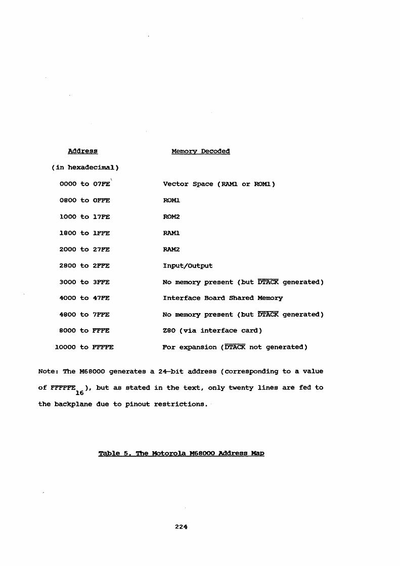
Address Memory Decoded(in hexadecimal)0000 to 07FE Vector Space (RAMI or ROMl)0800 to OFFE ROMl1000 to 17FE ROM21800 to IFFE RAMI2000 to 27FE RAM22800 to 2FFE Input/Output3000 to 3FFE No memory present (but DTACK generated)4000 to 47FE Interface Board Shaured Memory4800 to 7FFE No memory present (but DTACK generated)8000 to FFFE Z80 (via interface card)
10000 to FFFFE For expansion (DTACK not generated)
Note: The M68000 generates a 24-bit address (corresponding to a value of FFFFFE ), but as stated in the text, only twenty lines are fed to the backplane due to pinout restrictions.
Table 5. The Motorola H68000 Address Map
224

a = M /IO . ALOW . A13 . A12 . A l l . y
+ M /ÏÔ . ALOW . ÂÎ3 . A12 . A l l
B = M /ÏÔ . ALOW . S Ï3 . ÂÎ2 . Â Ï Î . 5c
+ M /ÏÔ . ALOW . ÂÏ3 . A12 . Â Ï Î
+ M /ÏÔ . ATOP . A13 . A12 . A l l 5c
c = M /ÏÔ . ALOW . ÂÎ3 . ÂÏ2 . A l l . y
+ M /ÏÔ . ALOW . A13 . Â Ï Î
a = M /ÏÔ . ALOW . Â Ï3 . ÂÎ2 . Â Î Î . X
+ M /ÏÔ . ALOW . A13 . ÂÎ2
+ M /ÏÔ . ATOP . A13 . A12 . A l l . X
lOS = M/IO . ÂÏ5 . Â Ï4 . AÏ3 . ÂÏ2 . Â Î Î
OFBD = ALOW + M /IO . ATOP. A13 . A12 . A l l
Not© : ATOP = A19 . A18 . A17 . A16 . A15 . A14
ALOW = ÂÏ9 . ÂÏ8 . ÂÏ7 . ÂÏ6 . ÂÏ5 . ÂÏ4
X and y are provided by the address map selection switches
a and b control the selection of the RAM devices
c and d control the selection of the ROM devices
lOS enables the input/output devices whilst OFBD controls
indicates that the memory requested is not on board.
Table 6. Intel 8086 Processor Board Memory and Inout/Output Decode
PAL contents
225

Ih Circuih Emula her Pod
Address Bus
Doha Bus
ROM
RAM
Microprocessor
Output
Input
Syshem ho be Examined
Fig 3.1 Exomination o^a Microcomputer Syshem by In Circuit Emulation

MiViicoinpuhcr Address Bus
Minicomputer Control Bus
Minicomputer Data Bus
MinicomputerInput/Output
Port
Minicompuhr ► D M AController-^
DMAControllerMinicomputer
Control
Direct Memory Access Channel
Micro- Proc.
Data /Address Transfers According to Minicomputer Bus Protocol
Input/Output Port Protocol
All M icrocom puter Control Address &Data Signals Treated Qs Minicomputer Data.
Controlled Only by Minicomputer Reassembles Data & Address
r Da^a /Address TVxiHsJers According ho Microcotnbufer
Protocol
^ s tïm ho be Exomined
RAM
Address Bus
Doha Bus
Conhrol Bus
ROM(Ophionol)
Fig. 3,2 Exominahon ConlTolled DirecP
Input*
Output
Ja Microcompuher 1^ Ext'emollg
tl" Mcworu Access Channel.
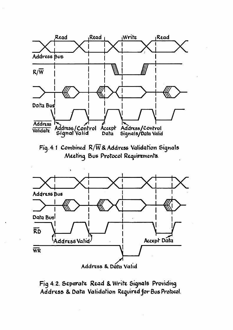
Read I Read iWrite
Addr4S8 pus
R/W
Doha Buj
Addmss
I I I
X Read
>
X€>
\ / r t \ \ A n h f Mdress/Control Accept A^rtss/Contnol Signal Valid Data ôiynals/Data Volid
Fig.4.1 Combined R/W& Address Validation Signals AAeehng Bus Protocol Regu'nnemcnts.
XXAddress Bus
>3
Data Bus!
Accept Data^Address ValidWR
Address & Data Valid
Fig 4.2. Separate Read & Write Signals Providing Address & Data Validation Required Jor Bus Protocol.

+ v
Motorola
MG800
/Address10
BusVMABus
3
-4 X 7 4L & 25 7
^ ^ S u s k m ' "Address Bus
Pull up Resistors Selected When V M A iO ,
Available (BA) Processor Address Bus Selected When VMA= f.
Multiplexer Outputs Enabled When BA=0 Disabled When BA=1
Resulh'.AII Involid.Cycles Read Reset Vector(FFFFjg,)
Fig 4 3 Circuit to Replace Valid Memory Address(VAM) Signal in AAotoroto M C 800 Systems.

Address on BusJ(Acv)
From FIOOL/DAU
I Hove Address^ m 2K(Pas)
From Memory
J (Pas)
From Memory I/o
Data Oh Bus
K(Acv)From FIOOL «
Bus Content Address
1
(Bits 0-15) ^
i) 1
/ I have Data
Data
H ig h
Low
HighLOW
HighLow
HighLow
HiqhLOW
HighLow
Fig 4.4 FI00 Read Onlu Cycle.
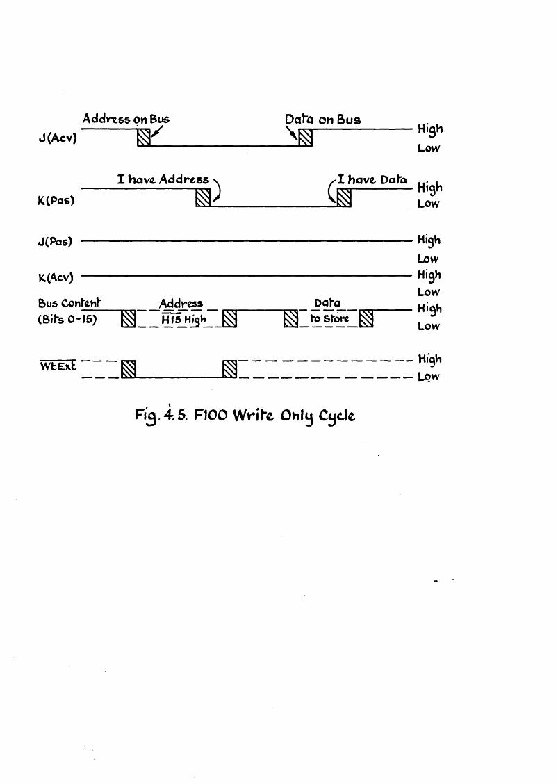
Address on Bus Dato on Bus . .j ( * c v ) — _______________________ h m ---------------------------------
Low
I hove Address \ / I have Doh%5>S \ /JL fl
#High
KlPos) ^ 1 ^ LOW
J(Pos) ----------------------------------------------------------------------------------------------- HighLow
K(Acv) ----------------------------------------------------------------------------------------------- HighLow
Bus Content Address Data
Low(Bits o - i i j ^ HIS High ^ ^ to Store ^
Fi j .45. FJGO Wri te Only Cycle

Address on Bus ,j ( A c v ) — m-------------- %From FIOOL or DMA
I have Address/ I Have D a t a .— Ë hm—2:LowFrom Memory
on Bus from Memory^ _ ,' ' c - ) m _0------ aK(Pas)
/Data ch Bus from Memory
From Memory I/O/% have Doha (F IO O L ) u*. u
K (A « ,------------------------g Ë ----------------------- - aFrom FIOOL ,Bus Content Address Data Data(B i ts %
W tE xb ~ ]~ | ^ ______________________________________ *^'9^Low
Fig 4.6 FI0 0 Read /Modi^/W tite

PgltRq,
PgltAcccpt
Link Stored & Lockout Latch S e t
(O)
XProgram Counter Processing Loaded With Conhnucs2048 o r 18584 From 2048
(b)
Fig 4.7 The FlOO-Unvectored Program IhtorruptS e q u e n c e
PgltRg 1
PgltAcctpt
As ta) As (b) Fig47 Fig 4.7
DAURg
DMA Accept
I
Processing Continues fro m 2046 + 2n o r
185844 Zn.
During this Time the Interrupting Device Should Transmitits Channel Number V Times! 2 to The I/O Bus~n r~
E x t U P g a“ > - r 7Taken Low Allowed bu the Device to Rise
bgFIOO-L
Fig 4 6. The F100 Vectored Program Interrupt Sec^oence
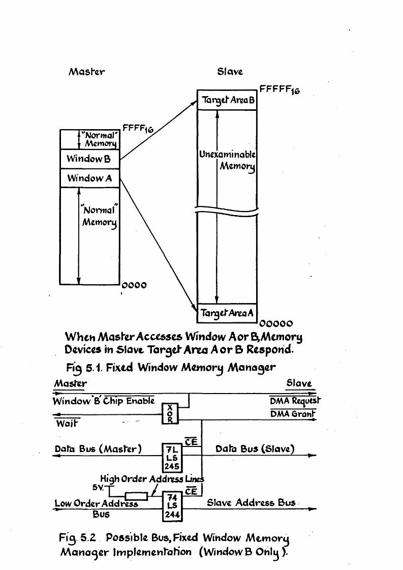
Masher Slave
UhcxominableM c w o » ^
Window B
0 0 0 0
oooooWhen Masher Accesses Window Aor B^Memortj Devices in Slove Tbrgeh Area A or B Respond.Fig 5 1 Fixed Window Memorg Manager
Master Slave
Window B Chip Enable
Waih
Doha Bus (Masher)
X1.
DMA RctjüCsh DMA Granh
7LL6245
CE
High Order Address Lines
Paha Bus (Slave)
i— r -Low Order Add t'es» 7 4
LSCEI
Slave Address BusBus 244
Fig 5,2 Possible Bus, Fixed Window M em ory M a n a g er ImplemenhaHon (W indowB Only ).
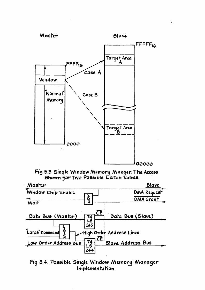
Mashtr Slav^
T û rg c l^ A reû
Window
NormalMcwonj
Case A
Cû5t B
F F F F F iQ>
OOOO
Target" Area
OOOOO
Fig 5.3 Single Window Memorg Manger. The Access Shown ^or Two Possible Latch Valves.
M aster SlaveWindow Chip Enable
W ait
Data Bus (M aster)
sR
DMA Rei^uest DMA Grant
Lateh CommandL
i74LSZ4S
CE
Low Order Address Bus
High Ordc CE
74LS244
Data Bus (Slave)
r Address Lines
Slave Address Bus
Fig 5.4. Possible Single Window M em ory M anagerImplementation.
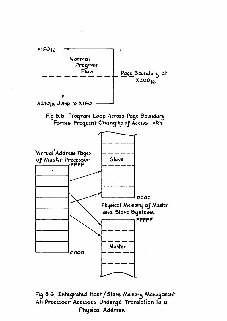
M F O t ô
NormalProgram
Page Boundorg ah X 2 0 0 ^ ^
XZtO|^ Jump ho XIFO
Fig 6.5 Program Loop Across Page Bouhdarg Forces Freguenh Changing o j Access Lohch.
Virhual Address Pagesof Masher Processor r-:------- i F F F f
Slave
1 0000
Phgsicol Memory o j Mosher and Slave Sushems -------------------FFFFF
0000
Fig 5 G Xnhegrahed Hosh/ Slave Memory Monogemenh All Processor Accesses Undergo Translahion ho q
Physical Address,

FFFF FFFFF
B as ic '
ROM£000
Eprom0000
EiHicr
Availablej^ o r
Expansion
- 8000Dynamic
RAM
Board I Map
Stahc RAM
Board
1000Norma) ZBO Address SpaceBoard I
OOOOOr
Memory Map of Masher ZBO When Memory Manoger is Disabled.
Fi^ 5 7. Mcmoi^ AAap oJ AAasher ZBO

A8-A15
A8-A11
AI9
Bus
A8-A16Reseh
O Vol he
ZÔOMicro
processor
Fig 5 8 Four to One MulHpkxcrs Selcchiig Address Source to be Fed to Sgstom Bus.
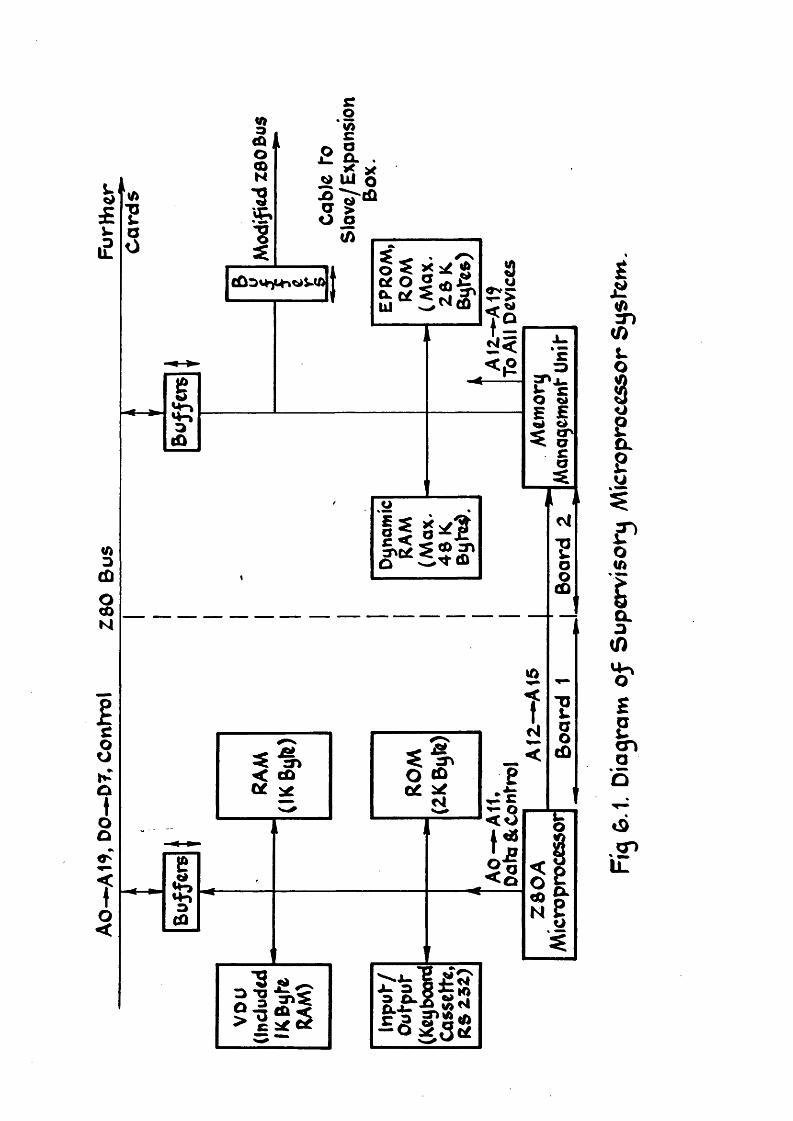
31
CD 31

z70
24 +5V 45V 45V23 A8 T AS AS22 A? M A9 8 A921 -5V Ô ypP K A1220 cs 2 OE R CE19 412 V 7 A10 0 A1018 PRGRM 1 CE M All17 D8 6 08 08
24 45V 45V23 A6 A8
2 22 A9 2 A97 21 Vpp 7 All1 20 OE 3 OE6 19 A10 2 A10
18 CE CE17 0 8 08
Fig 6,2 , Partial Pin-Oufe o j Eprows &Dosi/ROM
242322212 0191617
+5VA8A9
Dcfoull' Connection y / Provided by Pnnhed C rcü ^0 - 4 ) —o — o- o — o -
-5 VCE412VOV
45VAIDAllA12
Wire Wrap PinsX .
AllxmahVe Connecl'ione
Fig. 63 WiVfc WrapUhks Aliowmg Ahu of Above Eproms be Ahhed.
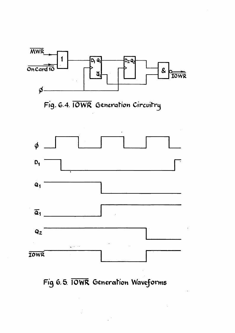
MWR
Oh Card 10lOWR
Fig. 6 4. lOWR Gcncrahon CiVcuilTu
D i
Q l
r
Û 1
Qz
lOW R
Fig 6.5, lOWR Gcticrahon Waveforms

(NIT MMU Di&ablc 1 0 R Q__________________ I- l U K m _________
MREQ 1 I I--------Firsh lns rücl' ono Q o n o o o ( S.0 1 2 3 4 6 6 7
Irjpofs 74 -L 5146
Az A| Ao
Rcsct'Sw'it'ches-
Titd Low -
Unmodif ltd Z60 Bus-
MMU Translohon RAMS-
0
12
3
74 L5 Z
5 3
Address Bus ^ A i 2 - * - A | 9
Fig 6 .6 UscoJ 7 4 L S 146 To Conf'rol A d d res sSource S tiech 'on
ÏÜRub74LSI46 Doha Source
s ig n a l Oufpul'on Af AO Sclcched
0 M REa 3 TranslaHon RAA^.
1 IN IT 2 IS O Bus Lines
z — 1 T ied Low
s — 0 Reset Switches
4 — 3 Translation RAMS.
5 M M U Disable 2 1 8 0 Bus Lines
6 lORQ 1 Tied Low
7 FirsK lh6^rucHon 0 Reset Switches
Incrtosing P rio rih j
Fig 6.7. 74LSI48 Signal AssignmenliG

Frame, § i Sync. 1U ~
Sync.
ZZOp
SVoIrs
Video Ouh
BCtSZBC18Z
OVolfe
Chanachor In fo rm q H o hMemory/10
128 Buie Block
Flyback Blanking Ihpul"
0 1 /iF
OVolhs
Fig 6.8*SoJy” Video Summing Circuit’
Bus Req.otsrNENIN
(Achive Low)INS 8080 NENOÜT
CAcHveLow)
Bus Available
Fig 6 9 The InFernol OR Gate Hie INS80G0 is Augmented bg the Fasher LSTTL OR Gate to Fonce Hie Video Buffers o j j Hie Bus M o re
QuicKlg.

HI/LO Select
From , Pcrsonalitu
Socket
From Processor Address Bus
A 4 A; Ai A o
A 9 —3 r |3 r ”î ~ | î ” 0 / 0 0 /o l s im i la r ly H ) 10 o 10 010 O I 6 Bit016 6 16 0 /0 o 10 j oirniiariy ! ® /° o lO 010 O #0 j *.
| _ i ± ___ 6 J 'Treated " |_ j___6_ _ 6 _
cea ceb Â3 Az A{ Ao To Bujj=er RAM
When an External Access is not Being Performed, Hie Personolitg Socket Provides A ^ & A0 to CI^.CEb -
Fig 6.10. Addressitw Scheme to Allow So^ly'Bu^er Access bg Eight ana Sixteen B it Processors.
5V
Close to Disable External Accesses, vw
6Vfsv-
A io XoR
Valid AddressI (Generated bg
EXTACC&
I \ Repeated fo r I Additional Addresso y J - A ifto A is I Decoding Can be Provided I by the Personality Bocket
Through Valid Address
Fig. 6.11 So tg Selection Circuit.

Ext*crnalB u g
S q ffyBus
All BuJJtrs ore 74LS245Low Byl"t (All Accesses)
Fi . 6.l2.So5*hj RAM B u jftr Layout

PinNumber
125456
78
91 011121314
FuncHon
22c22a21c20c20a19c18c17c10c15C14c15c
From Edge Connecl'or
PinNumber
282726252423222120191817
5 Q(A0 ofExt-.MPU) 16 O Voll-8 15
FuncHott
SVoll-sC E b
c e aR/WVA*Sof|-y AO EXTACC19q 18a I7q 16a 15a 14a 13a
FromEdge
Connector
Edge Connecl'or Signals are Hiosefrom Ihc Area Reserved ^or Control Signals, buh are Otherwise Undefined.
1
Fig 6 1 3 *Sof l'y Personalil'y SockeT P/nouh
A\6800<11
VAtAO o - . (17)
02 o -_ (6)
R/W o -
&
( * ) Indicates Personality Socke^ Pin Number
&
' S o f T y
(25) _- o R/W
AO ^om SoJIy'(2V
o Ctiipenqble B
( 2 0 — :------------------Ctupenable A
Fiy. 6.14 M 6800-^5(^ ly Personality Socket'Circuit:

Z B O Sojt'y
MREQo
— (7) RO o-
.)£(X
(21)W R O —
&
( * ) Indicates Personality Socket' Pin Number,
3-------
&
D-------
(2 4 ) _ —o VA
^ ” r / w
(27)"O Chipcnable B
&(26)
ChipenableA
Fig 6.15 ZSO-^Soÿt'g" Personalil'y Sockeb Circuit"
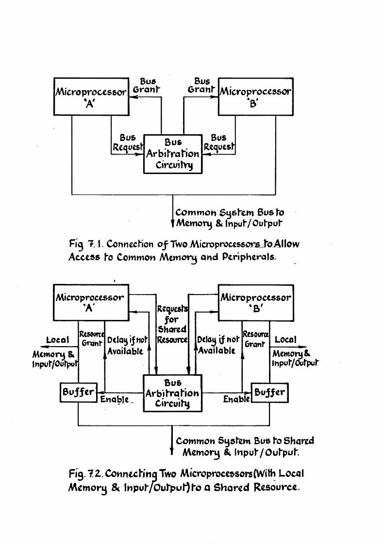
Bus BusRequest*
Common Syshem Bus to M e m o r y & ln p u ^ /O u ^ p u ^
MicroprocessorMicroprocessor
f i a 7.1. ConnecHon o f Two^MicroproccssorfiJoAllow Access ho Common Memory and Peripherals.
RtsouretGronfDelay if nol*
AvailableLoco!Local
Common System Bus ho Shared Memory & . Inpuh/Ouhpuh.
B uffer
Microprocessor Microprocessor
Fig 72. Connechinq Two Microproce&sors(Wilh Local Memory & lnpuh/Outpuh)ho o Shared Resource.
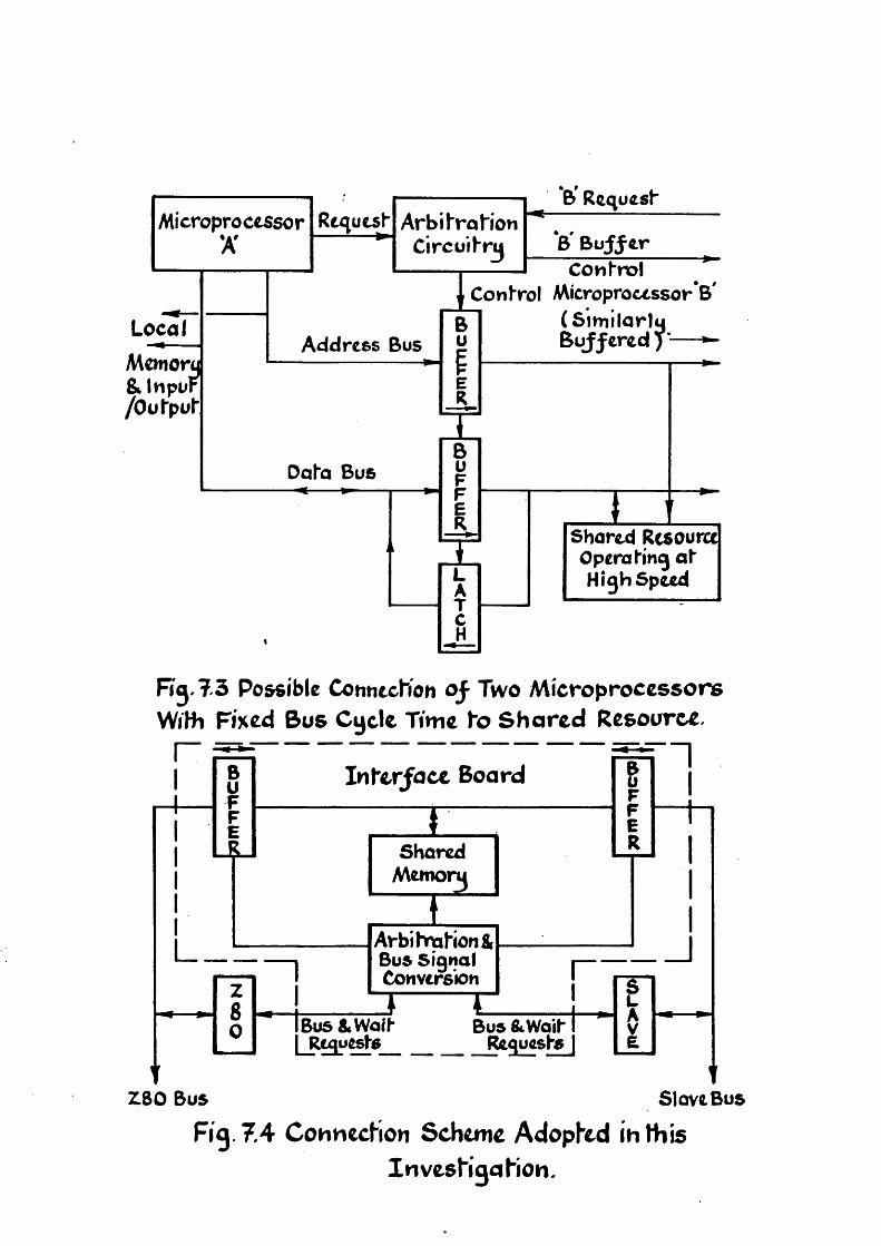
Microprocessor Reguesl" ArbihrahonCircüihry
& Rcquesh
B' B u jj^ e r
Cohhrol
LocalMcmoru & Inpur /OuTpuf
Address Bus
^onhrol Microprocessor B'Bu
;ER
(Simllartu BuJJered y
Doha BusBuFFILATH
Shored Resource Operohng at' Highspeed
Fig,? 3 Possible Connechon o j - Two M icroprocessors Wilh Fixed Bus Cycle Time ^o S h ared Resource,
I BFFE
A
Inherjoce Board
IShored
M e iro y ^
gFFER
Z80
I
A r b ifm h o n & Bus signal Conversion
1 1Ibus&Wo: Bus&WaihI Rcquesfs__________Requeshs
Z80 Bus SloveBus
Fig 7,4 CohMccHon Scheme Adophtd ih thisIn v e s h 'g a t’ioiri,

B o o rd s d M l'
BA-------
XOK
&
R/W
XoR
Enable Conlnol oJ74L6Z45on
Do^a Bus
oirecHoM Confrol o f 74LS245 on
Data Bus.
Fig. 8.1 DtrivaHoh MB800 Doha Bus BuJJcrControl signals.
< ^ i
z%fc
VMA—
Fig 8.Z GeneraMon o f Modified VM A^or Use onIn^c.rJoce Board
S M R .Ô W -
I/OSÊL.&
SMA
i m&
z s o ÿ
Z80 T T ^ Î
iF
m rr7407
Fig 8.3 ZSO.Wail'Stal'eGcncration CiVcoih
MEMCUC
Z x f c
1Hold
0 Q>
. Holdl { > — -
7407
Fig 8.4 A\G800 ^1 Hold Regues Sgncrohisahon

zxfc
NA
Fig. 8,5 02 S re ching Circoil;M&600—Z80Acc«&s€s
Mem ROYBA
O M S
BA
Fig 8.6 0 2 S l'rtf’chmg Circuih^ISO-^-M6800 Accesses
NA
ZÂV
BACK,
Open Collecter — BRÊÔ
7407
1 BACKI
Fig 8.7 GeneroHoh of a BACKSignol Mioh isOnlg Prcschkd h> Hie Interface Ajtcron M0800
In itiated Z80 Bus Rcgucst.

65000 ' Clock
WAIT
ÜÔ5 5V olk .0-1
l d S
Syshim
DTACK
DTEN
OhBoanJ
(*)Thc Number o j Flip-Flops in the Chain Dehermines Hie Bus Cycle LenaMi
FÎ0 . 8.8 M 68000 DTACK Generah'on Circuih

A&
O M S
D R
Z 6 0 WAIT
Z80,
ElZb E44d
E5Z E52
Fig 8.9.M 68000 BGACK&Z80Wcl t'Gene^a 'iohClrc4 l
Z 8 0 M&8000
La t’en
Low
High
Fig, 8.10, M 68000 Ihhirjocc Boord Dolb PoHis

A g
3 ) 5 O
o CÛ
fS A Q *
0 6 ocr
O
LU
O
«a
O lü
îfV
IC
OU)
30 <10CDM
8
1o o oCOo
00dr>
Ll

1 R0M1 1 R0M1 1 1 RAMI 1 RAMI 1
;1
ROM 2 RAM 2 R0M2 RAM2R0M1 ROMI RAMI RAMI
X=1 X=1 X=0 X=0>i-o y=1 y = 0
FFFFF
MemoryMap
00000
Fig. 8.12. Possible RAM/ROM Combinahons qj' Inhd 8086 Reseh / Inl'erropt' LocaMons.
I / o Mop
P10PIC
USAKTLEDS
FFFF
Board
400 0
02000018001000080000
Memory MapFFFFFRAMI/R0M1
180
-R0M2I2O M IROMRAM2RAMI
RAM2/R0MZRAM1/R0M1
FF800
10000
08000
04800040000380003000028000200001800010000080000000
Fig. 8.13 Iht'el 8086 Memory & Ihpu /Out'put Map.
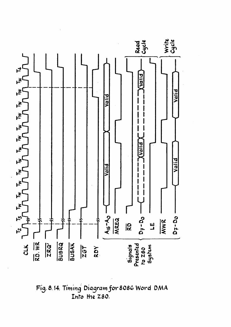
I ?
l^ '
I? '
"PHU-Ju
rO
\ uN
r
L 1
II
fis< Il
rOC£
5rI III I 11u
L
I I
YIh-O UJ
,eri(^ <(0 ü)
jZ) 3 Icû IcÛ
KON
>“Ot f
2 ; S j
4 2
Î 5 '
a>
$
Ftg.ô. 14. Timing Dicgram^orSOSC Word DMA I n r o H ie Z 8 0 .

POLESTAR
ADVANCE PRODUCT INFORMATION
NEW CONCEPT IN UNIVERSAL MICROPROCESSOR APPLICATIONS DEVELOPMENT AND EDUCATION
THE POLESTAR SYSTEM PROVIDES A LOW COST ENTRY INTO UNIVERSAL MICROPROCESSOR APPLICATIONS DEVELOPMENT WHICH IS CAPABLE OF CONTINUOUS EXPANSION TO A DISK BASED SYSTEM WITH FULL IN-CIRCUIT EMULATION FACILITIES SUPPORTING ALL THE POPULAR FAMILIES OF 8 BIT AND 16/32 BIT MICROPROCESSORS. EDUCATIONAL USERS CAN START WITH A LOW COST SINGLE BOARD STUDENT POSITION RUNNING OVER 30 K BYTES OF FIRMWARE WITH 8 K OF USER MEMORY PROVIDING SOPHISTICATED ASSEMBLY PROGRAMMING FACILITIES. MULTIPLE STATIONS OF THIS TYPE CAN BE LINKED VIA OUR POLESTAR LOCAL AREA NETWORK TO A CENTRAL DISK BASED HOST, ALLOWING SHARING OF DISK AND PRINTING FACILITIES BY EACH STUDENT.ITSSIRIUS MICROTECH LTD
Spring Lane South, Malvern Link, Worcs. Telephone: Malvern (06845) 66973
SHORT SPECIFICATION POLESTAR SYSTEM# Z80A host with 64 K bytes.e System UART RS232 User UART RS232.
System PIC User RIO.# Target processor interface for 8/16 bit processors with high speed buffer.# 600/1200 baud cassette interface.# EPROM read/burn socket on front panel under software control for 2708,2716,2532,2732,2764.# Power supply meeting most expansion requirements including floppy disk drives.
POLESTAR OPTIONS# 128 K main memory.# Low cost intelligent VDU controller for attached keyboard/monitor.# Dynamically relocatable memory display of 512 bytes on separate monitor providing display of any
512 byte memory area or the last 512 bytes of I/O under software control.# Floppy disk system - two double density 8 inch drives with controller.# Polestar local area network.# VDU's, printers, etc.# Educational board with buffered PIG for relays, lamps, etc. plus A/D and D/A capability.
TARGET PROCESSORS# Target chip set sockets for 8 x 2732 plus up to 8 K RAM, SIC (RS232), PIG.# Polestar target processors-with modular personality firmware interfacing with system firmware and
monitor to provide editor/assembler personalised to target.Supporting^68000, Z8000,8086-6800,8085, Z80,6502 farnjiies (othersto fqllow)._^ __
# Polestar in-circuit emulation - basic module plus personality modules for each processor supported providing probe/trace/event/trigger facilities with conditional operators and nested conditional statements under software control of disk based system.
# Student position can consist of any supported target processor running under the full Polestar firmware with 8 K of user memory and a CRTC handling a keyboard and screen. A power supply and 600/1200 baud cassette interface is provided to give a stand alone capability. A local area network interface is optional.
SOFTWARE/FIRMWARE# Gver 30 K of firmware provides a sophisticated development capability without disks.
6 K monitor - editor - assembler - debug - disassembler - basic interpreter-test routines (diagnostics). Personalised to target by modules on target board.
# Software designed to run under *CP/M 2.2 DGS providing - monitor - editor - assembler - debug - disassembler-linker plus diagnostics. Local area network handler providing students with controlled access to disk and printing facilities. In-circuit emulation package.
# High level language support - PASCAL (others to follow).
# Trade Mark of Digital Research Inc.
Since our policy is one of continuous Improvement this specification may be subject to change without notice.
mSIRIUS MICROTECH LTDSpring Lane South, Malvern Link, Worcs. Telephone: Malvern (06845) 66973