DR.S.M.THIRUNUAVUKKARASU MD., DEPARTMENT OF MEDICINE GOVT. THENI MEDICAL COLLGE THENI.
International Journal of Advance Research In Science And Engineering http://www.ijarse.com
IJARSE, Vol. No.4, Special Issue (01), March 2015 ISSN-2319-8354(E)
113 | P a g e
A MOSFET AND CNTFET BASED DESIGN OF
MULTIVALUED LOGIC
Jakkammal @Malarvizhi.S1, Latha.A
2, Srinidhi.S
3
1, 2PG Scholar, Department of VLSI Design,
3Assistant Professor
Theni Kammavar Sangam College Of Technology, Theni,Tamilnadu, (India)
ABSTRACT
In modern VLSI systems a large proportion of power is consumed by interconnect and switching. The reduction of
static and dynamic power dissipation are the major challenges in the rapid growth of the VLSI technology. With the
emerging nanometric technologies, Multiple valued logic(MVL) circuits have attracted significant attention due to
its advantages in information density and operating speed. The main contributions include the implementation of
Ternary logic in the Carbon Nano Tube FET’s (CNTFET) and their various performance metrics like static power
consumption, propagation delay and power delay product are compared with the existing MOSFET based ternary
logic gates. Compared to the complementary logic family the pseudo – NCNTFET MVL logic family requires a
smaller circuit area with a similar propagation delay on average, with a larger power delay product and static
power consumption.
Keywords: Multiple valued logic, carbon nanotube field-effect transistor, ternary logic, power delay
product.
I. INTRODUCTION
The scaling of CMOS technology has not brought significant improvements in integrated circuits, but it has also
raised the power consumption in advance digital designs. As CMOS approaches physical and technological limits,
new devices have been proposed to implement nanoscale circuits, such as those based on multiple-valued logic
(MVL). Traditionally the digital computation is performed on two valued logic, i.e., there are only two possible
values (0 or 1, true or false) in the Boolean space. Multiple-valued logic allows more than two levels of logic;
implementations of ternary, quaternary, penta for various applications. MVL enjoys many advantages over its binary
counterpart; for example, each wire can transmit more information, so that the number of interconnections in the
chip can be reduced, resulting in a lower circuit complexity. In particular, CNTFETs have attracted significant
attention as an alternative to silicon-based Mosfets for implementing MVL gates due to its potential advantages such
as high mobility of charge carriers.
International Journal of Advance Research In Science And Engineering http://www.ijarse.com
IJARSE, Vol. No.4, Special Issue (01), March 2015 ISSN-2319-8354(E)
114 | P a g e
II. MULTI VALUED LOGIC
Multiple-valued logic allows more than two levels of logic; implementations of ternary, quaternary, penta for
various applications. MVL enjoys many advantages over its binary counterpart; for example, each wire can transmit
more information, so that the number of interconnections in the chip can be reduced, resulting in a lower circuit
complexity. Multi value logic replaces the classical Boolean characterization of variables with either finitely or
infinitely many values such as ternary logic.
With an increasing density of chips, the number of inter chip connections is greatly increased as more and more
functions are put on the same chip; thus, the size and performance of the chip is mostly dominated by wiring rather
than devices. One of the most promising approaches to solve the interconnection problems is the use of multiple-
valued logic (MVL) inside the VLSI chip. The number of interconnections can be directly reduced with multiple-
valued signal representation. The reduced complexity of interconnections makes the chip area and the delay much
smaller than others.
From the view point of reduction of interconnections, advantages of K-valued logic system in submicron VLSI is
chip density. The chip area in submicron VLSI is almost determined by the interconnections. In K valued logic the
number of interconnections can be reduced to1 / log2 K in comparison with binary logic. If this effect can be applied
to 2-dimensional geometry, the reduction ratio becomes 1/(log2 K)2 .
The total area of interconnections is determined by the number of interconnections and their length. The
interconnection length is also determined by the complexity of the interconnections, so that it is clear that the use of
MVL is very useful for compact VLSI implementation.
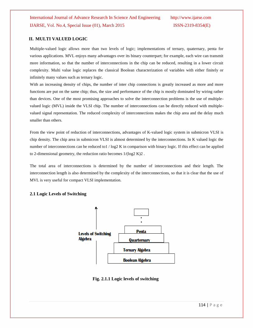
2.1 Logic Levels of Switching
Fig. 2.1.1 Logic levels of switching
International Journal of Advance Research In Science And Engineering http://www.ijarse.com
IJARSE, Vol. No.4, Special Issue (01), March 2015 ISSN-2319-8354(E)
115 | P a g e
Logic gates constitute the foundation blocks for digital logic. Traditional binary gates are use in current digital
devices. The multivalued logic gates have not been standardized but ternary and quaternary gates are two
commonly used multivalued logic gates described in literature.
2.2 Ternary Logic
The most generally used switching circuit components today are two-valued or binary. The electrical conditions
controlling these switching circuit components are also generally two-valued or binary. But integrated circuits can
now handle multiple valued signals & switching at high speed rather than binary signals, especially at data
communication level because of the reduced interconnections & switching [6].
Utilization of multi valued logic (MVL) reduces the number of signals involved in the communication, increasing
their information content. In such a way, an interconnection-limited design can be realized with MVL like for the
asynchronous circuits and comparable performance than a classical binary design may be obtained [7]. Among
various types of MVL, the ternary logic receives more attention than others because of lower interconnection cost
estimation and a simple electronic circuit implementation method [8].
Ternary and quaternary circuits have been studied increasingly in recent years. Quaternary circuits have the practical
advantage that a four-valued signal can easily be transformed into a two-valued signal. However, based on the
following considerations, we feel that ternary circuits may be of more theoretical significance than others:
Since 3 is the smallest radix higher than binary, ternary functions and circuits have simpler form and
construction. They can be studied and discussed easily, yet they still display the characteristics of
multivalued elements.
As a measure of the cost or complexity of multi- valued circuits, the product of the radix and the
number of signals has been proposed. Since 3 is the digit nearest to e = 2.718, ternary circuits will be
more economical according to this measure.
If balanced ternary logic (1,0, - 1) is used, the same hardware may be used for addition and for
subtraction.
Since 3 is not an integral power of 2, research on ternary logic may disclose design techniques that are
overlooked in the study of binary or quaternary logic.
Ternary gates are designed by the standard MOS technology in two ways. In one way, dynamically controllable
circuits are suggested. Here it is necessary to include special clock oscillators that occupy a considerable area on
the crystal and can cause an excess number of switching events and excessive noise components in digital
circuits. The other way implies the design of ternary circuits that do not require any supplementary control
signals.
International Journal of Advance Research In Science And Engineering http://www.ijarse.com
IJARSE, Vol. No.4, Special Issue (01), March 2015 ISSN-2319-8354(E)
116 | P a g e
2.3 Scope of Multivalue Logic
Since inception digital devices have been designed using binary logic till date. Researchers have found the
development in binary logic is cumbersome, complex and difficult to understand. Since multivalued logic enables
more information to be packed in a single digit researchers have been working on multivalued logic for many years
[1]-[3]. With development of novel electronic devices and optical devices, it is now possible to implements circuit
for more complicated logic system [4]-[6].
Many of these devices are capable of dealing with more than two logic states but they are at experimental stage.
Some multivalued logic systems such as ternary and quaternary logic schemes have been developed but successful
implementation is yet to become available.
Ternary logic has several advantages over binary logic. Since it require half the number of digits to store any
information than its binary equivalent it is good for storage; the ternary storage mechanism is less than twice as
complex as the binary system.
Though their design principles of resistive loaded designs are valuable in various factors, they still suffer from
large static power consumption due to the presence of resistors. Compared to the resistive loaded design the
complementary logic family shows some improvement. But above all, the implementation of pseudo logic in the
basic set of logic gates like inverter, nand and nor gate are presented in this project shows an efficient result and
compared with the above implementations.
III. WAY OF IMPLEMENTING TERNARY LOGIC
3.1 MOSFET
CMOS integrated technology is considered to be the best choice for implementing the ternary logic circuits for the
following reasons:
1. CMOS multivalued circuits are expected to share three principal advantages of CMOS binary circuits:
zero static power dissipation in either stable state, low-output impedance in either state or elimination
of passive elements (resistors).
2. Any multivalued signal can be transmitted through a CMOS transmission gate.
3. In contrast with the pn-junction threshold of a bipolar transistor, the MOS transistor's threshold may
easily be changed during fabrication, simplifying the task of responding to a multilevel input signal.
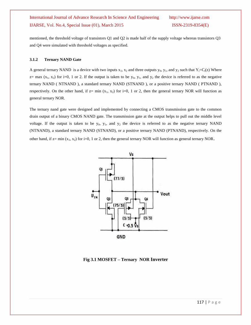
3.1.1 Ternary Inverter
For the ternary inverter the inputs are given as {0, 1, 2} and it yields the output {2, 1, 0}. Because of its ability to
produce {1} at the output, ternary inverter is used as the primary building block for the proposed SRAM cell and its
CMOS implementation is based on the design in [2]. A high resistance transmission gate is connected between the
output of a low-resistance threshold modified binary inverter and 0.5Vs to produce the middle level voltage [1]. As
International Journal of Advance Research In Science And Engineering http://www.ijarse.com
IJARSE, Vol. No.4, Special Issue (01), March 2015 ISSN-2319-8354(E)
117 | P a g e
mentioned, the threshold voltage of transistors Q1 and Q2 is made half of the supply voltage whereas transistors Q3
and Q4 were simulated with threshold voltages as specified.
3.1.2 Ternary NAND Gate
A general ternary NAND is a device with two inputs x1, x2 and three outputs y0, y1, and y2 such that Yi=Ci(z) Where
z= max (x1, x2) for i=0, 1 or 2. If the output is taken to be y0, y1, and y2 the device is referred to as the negative
ternary NAND ( NTNAND ), a standard ternary NAND (STNAND ), or a positive ternary NAND ( PTNAND ),
respectively. On the other hand, if z= min (x1, x2) for i=0, 1 or 2, then the general ternary NOR will function as
general ternary NOR.
The ternary nand gate were designed and implemented by connecting a CMOS transmission gate to the common
drain output of a binary CMOS NAND gate. The transmission gate at the output helps to pull out the middle level
voltage. If the output is taken to be y0, y1, and y2 the device is referred to as the negative ternary NAND
(NTNAND), a standard ternary NAND (STNAND), or a positive ternary NAND (PTNAND), respectively. On the
other hand, if z= min (x1, x2) for i=0, 1 or 2, then the general ternary NOR will function as general ternary NOR.
Fig 3.1 MOSFET – Ternary NOR Inverter
International Journal of Advance Research In Science And Engineering http://www.ijarse.com
IJARSE, Vol. No.4, Special Issue (01), March 2015 ISSN-2319-8354(E)
118 | P a g e
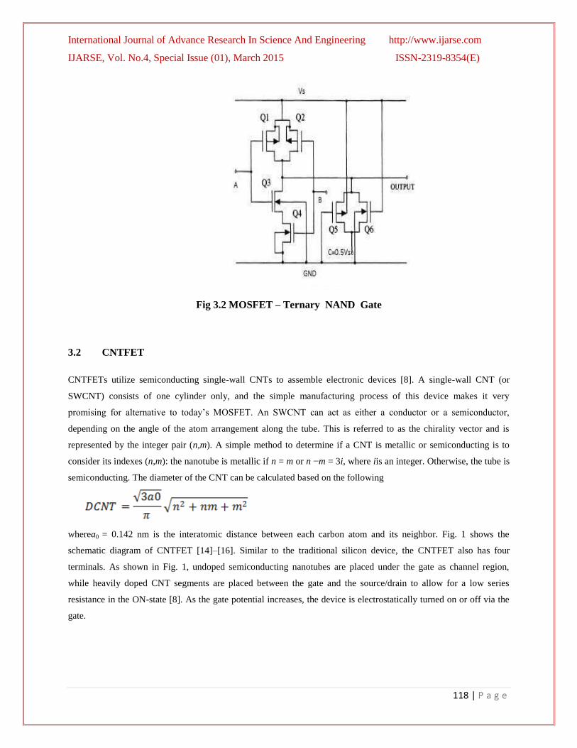
Fig 3.2 MOSFET – Ternary NAND Gate
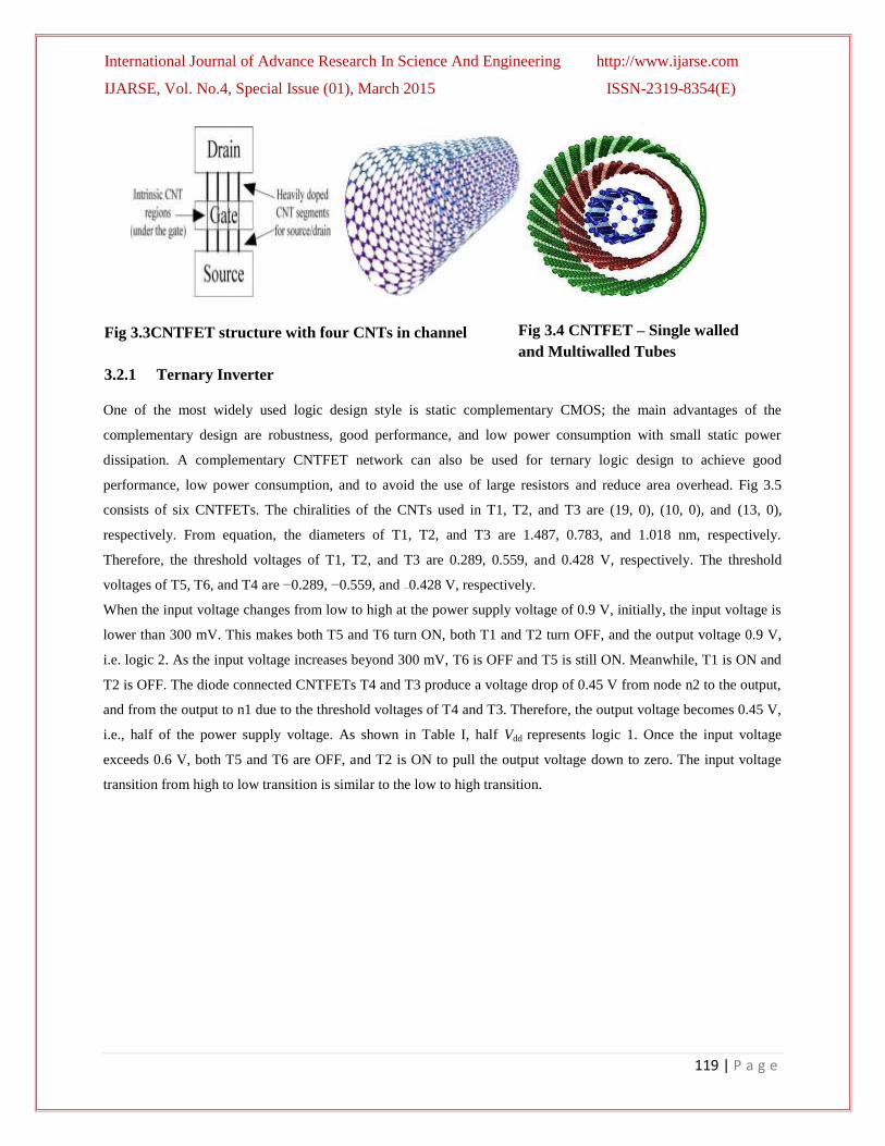
3.2 CNTFET
CNTFETs utilize semiconducting single-wall CNTs to assemble electronic devices [8]. A single-wall CNT (or
SWCNT) consists of one cylinder only, and the simple manufacturing process of this device makes it very
promising for alternative to today’s MOSFET. An SWCNT can act as either a conductor or a semiconductor,
depending on the angle of the atom arrangement along the tube. This is referred to as the chirality vector and is
represented by the integer pair (n,m). A simple method to determine if a CNT is metallic or semiconducting is to
consider its indexes (n,m): the nanotube is metallic if n = m or n −m = 3i, where iis an integer. Otherwise, the tube is
semiconducting. The diameter of the CNT can be calculated based on the following
wherea0 = 0.142 nm is the interatomic distance between each carbon atom and its neighbor. Fig. 1 shows the
schematic diagram of CNTFET [14]–[16]. Similar to the traditional silicon device, the CNTFET also has four
terminals. As shown in Fig. 1, undoped semiconducting nanotubes are placed under the gate as channel region,
while heavily doped CNT segments are placed between the gate and the source/drain to allow for a low series
resistance in the ON-state [8]. As the gate potential increases, the device is electrostatically turned on or off via the
gate.
International Journal of Advance Research In Science And Engineering http://www.ijarse.com
IJARSE, Vol. No.4, Special Issue (01), March 2015 ISSN-2319-8354(E)
119 | P a g e
Fig 3.3CNTFET structure with four CNTs in channel
3.2.1 Ternary Inverter
One of the most widely used logic design style is static complementary CMOS; the main advantages of the
complementary design are robustness, good performance, and low power consumption with small static power
dissipation. A complementary CNTFET network can also be used for ternary logic design to achieve good
performance, low power consumption, and to avoid the use of large resistors and reduce area overhead. Fig 3.5
consists of six CNTFETs. The chiralities of the CNTs used in T1, T2, and T3 are (19, 0), (10, 0), and (13, 0),
respectively. From equation, the diameters of T1, T2, and T3 are 1.487, 0.783, and 1.018 nm, respectively.
Therefore, the threshold voltages of T1, T2, and T3 are 0.289, 0.559, and 0.428 V, respectively. The threshold
voltages of T5, T6, and T4 are −0.289, −0.559, and −0.428 V, respectively.
When the input voltage changes from low to high at the power supply voltage of 0.9 V, initially, the input voltage is
lower than 300 mV. This makes both T5 and T6 turn ON, both T1 and T2 turn OFF, and the output voltage 0.9 V,
i.e. logic 2. As the input voltage increases beyond 300 mV, T6 is OFF and T5 is still ON. Meanwhile, T1 is ON and
T2 is OFF. The diode connected CNTFETs T4 and T3 produce a voltage drop of 0.45 V from node n2 to the output,
and from the output to n1 due to the threshold voltages of T4 and T3. Therefore, the output voltage becomes 0.45 V,
i.e., half of the power supply voltage. As shown in Table I, half Vdd represents logic 1. Once the input voltage
exceeds 0.6 V, both T5 and T6 are OFF, and T2 is ON to pull the output voltage down to zero. The input voltage
transition from high to low transition is similar to the low to high transition.
Fig 3.4 CNTFET – Single walled
and Multiwalled Tubes

International Journal of Advance Research In Science And Engineering http://www.ijarse.com
IJARSE, Vol. No.4, Special Issue (01), March 2015 ISSN-2319-8354(E)
120 | P a g e
Fig 3.5 CNTFET – Ternary Inverter
Fig 3.6 CNTFET – Ternary NAND
International Journal of Advance Research In Science And Engineering http://www.ijarse.com
IJARSE, Vol. No.4, Special Issue (01), March 2015 ISSN-2319-8354(E)
121 | P a g e
3.2.2 CNTFET - Ternary NAND
The circuits for the two-input ternary NAND is shown in Fig 3.6 respectively. Each of these two gates consists of
ten CNTFETs, with three different chiralities. They are essentially the same as their binary CMOS counterparts,
except for the transistors of different threshold voltages. In these two gates, similar to the STI circuit of Fig 3.5, the
transistors with diameters of 1.487, 0.783, and 1.018 nm have threshold voltages of 0.289, 0.559, and 0.428 V,
respectively, as established using threshold voltage.
IV. PSEUDO LOGIC
4.1 PSEUDO NCNTFET Ternary Gates
Pseudo-NMOS logic is an example of ratio-ed logic which uses a grounded PMOS load and an NMOS pull-down
network that realizes the logic function [5]. The main advantage of this logic is it uses only N+1 transistors verses
2N transistors for static CMOS. In this logic the high output voltage for any gate is Vdd and the low output voltage
is not 0volt. This results in decreased noise margin.
The main drawback of this logic is very high static power consumption as there exists a direct path between Vdd and
ground through the PMOS transistor. In order to make low output voltage as small as possible, the PMOS device
should be sized much smaller than the NMOS pull-down devices. But to increase the speed particularly when
driving many other gates the PMOS transistor size has to be made larger. Therefore there is always a trade-off
between the parameters noise margin, static power dissipation and propagation delay.
When the input is logic 0, TN1, and TN2 in all three designs [as shown in Fig 3.7 are OFF . Since the output is
expected to be logic 2 and the P-type CNTFET has a strong capability to transfer a high voltage, TP1 and TP2 in
the pseudo-NCNTFET STI [see Fig 3.5] are both working in the deep triode region (or deep linear region). The
equivalent resistances of TP1 and TP2 are small and negligible, as shown in Fig 3.7. TP3 and TP2 in a
complementary STI [see Fig 3.5] are both turned ON and operate in the deep triode region. Therefore, the static
power consumptions for all three designs are very small under this scenario, as confirmed by the SPICE simulation
results.

International Journal of Advance Research In Science And Engineering http://www.ijarse.com
IJARSE, Vol. No.4, Special Issue (01), March 2015 ISSN-2319-8354(E)
122 | P a g e
Fig 3.7 Pseudo NCNTFET Ternary Inverter
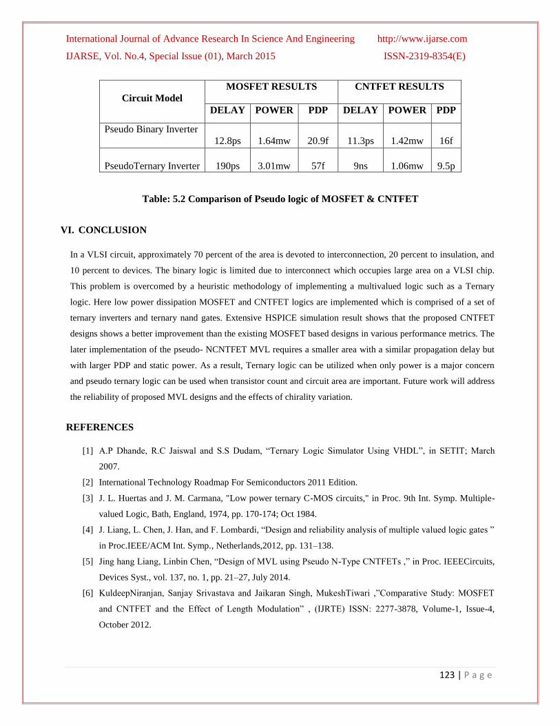
V. COMPARISON OF MOSFET and CNTFET
Binary and ternary logic gate function inverter and NAND logic are designed in both CMOS and CNTFET
technologies. Power reduction is achieved in the ternary logic with the marginal cost of delay and hence the power
delay product. Compared to MOSFET power delay product CNTFET shows greater reduction in power which is
shown in the below table.
Circuit Model
MOSFET RESULTS
CNTFET RESULTS
DELAY POWER PDP DELAY POWER PDP
BINARY_INVERTER
24ps
886uw
21.2f
22ps
48uw
1f
TERNARY_INVERTER
9ns
190uw
1.7p
8ns
6uw
48f
BINARY_NAND
60ps
704uw
42.2f
40ps
49uw
1.9f
TERNARY_NAND
10ns
277uw
2.7p
9ns
8uw
72f
Table: 5.1 Comparison of CMOS vs CNTFET for Inverter and NAND Gates
International Journal of Advance Research In Science And Engineering http://www.ijarse.com
IJARSE, Vol. No.4, Special Issue (01), March 2015 ISSN-2319-8354(E)
123 | P a g e
Circuit Model
MOSFET RESULTS
CNTFET RESULTS
DELAY POWER PDP DELAY POWER PDP
Pseudo Binary Inverter
12.8ps
1.64mw
20.9f
11.3ps
1.42mw
16f
PseudoTernary Inverter
190ps
3.01mw
57f
9ns
1.06mw
9.5p
Table: 5.2 Comparison of Pseudo logic of MOSFET & CNTFET
VI. CONCLUSION
In a VLSI circuit, approximately 70 percent of the area is devoted to interconnection, 20 percent to insulation, and
10 percent to devices. The binary logic is limited due to interconnect which occupies large area on a VLSI chip.
This problem is overcomed by a heuristic methodology of implementing a multivalued logic such as a Ternary
logic. Here low power dissipation MOSFET and CNTFET logics are implemented which is comprised of a set of
ternary inverters and ternary nand gates. Extensive HSPICE simulation result shows that the proposed CNTFET
designs shows a better improvement than the existing MOSFET based designs in various performance metrics. The
later implementation of the pseudo- NCNTFET MVL requires a smaller area with a similar propagation delay but
with larger PDP and static power. As a result, Ternary logic can be utilized when only power is a major concern
and pseudo ternary logic can be used when transistor count and circuit area are important. Future work will address
the reliability of proposed MVL designs and the effects of chirality variation.
REFERENCES
[1] A.P Dhande, R.C Jaiswal and S.S Dudam, “Ternary Logic Simulator Using VHDL”, in SETIT; March
2007.
[2] International Technology Roadmap For Semiconductors 2011 Edition.
[3] J. L. Huertas and J. M. Carmana, "Low power ternary C-MOS circuits," in Proc. 9th Int. Symp. Multiple-
valued Logic, Bath, England, 1974, pp. 170-174; Oct 1984.
[4] J. Liang, L. Chen, J. Han, and F. Lombardi, “Design and reliability analysis of multiple valued logic gates ”
in Proc.IEEE/ACM Int. Symp., Netherlands,2012, pp. 131–138.
[5] Jing hang Liang, Linbin Chen, “Design of MVL using Pseudo N-Type CNTFETs ,” in Proc. IEEECircuits,
Devices Syst., vol. 137, no. 1, pp. 21–27, July 2014.
[6] KuldeepNiranjan, Sanjay Srivastava and Jaikaran Singh, MukeshTiwari ,”Comparative Study: MOSFET
and CNTFET and the Effect of Length Modulation” , (IJRTE) ISSN: 2277-3878, Volume-1, Issue-4,
October 2012.
International Journal of Advance Research In Science And Engineering http://www.ijarse.com
IJARSE, Vol. No.4, Special Issue (01), March 2015 ISSN-2319-8354(E)
124 | P a g e
[7] Kyung-Hoae Koo, HoyeolCho,PawanKapur, And Krishna C. Saraswat“Performance Comparisons Between
Carbon Nanotubes, Optical, And Cu On-Chip Interconnect Applications”-IEEE Transactions On Electron
Devices, Vol. 54, No. 12, December 2007.
[8] S. Lin, Y. Kim, and F. Lombardi, “CNTFET-based design of ternary logic gates and arithmetic circuits,”
IEEE Trans. Nanotechnology., vol. 10, no. 2, pp. 217–225, Mar. 2011.
[9] TomazFelicijan and Steve B. Furber,” An Asynchronous Ternary Logic Signaling System,” IEEE
Transactions On Very Large Scale Integration (VLSI) Systems, Vol. 11, No. 6, December 2003.
[10] Wu, X.W., Prosser, F.P. “CMOS ternary logic circuits,” Circuits, Devices and Systems, IEEE Proceedings,
Volume: 137 Issue: 1, pp: 21 – 27, Feb 1990.
BIOGRAPHICAL NOTES
MS.S.JAKKAMMAL @ MALARVIZHI is presently pursuing M.E final year in Electronics and Communication
Engineering Department ( specialization in VLSI design) from TheniKammavarSangam College of Technology,
Theni, Tamilnadu, India. She completed her Bachelor of Engineering (ECE) from Anna University, Chennai,
Tamilnadu in the year 2009.
MS.A.LATHA is presently pursuing M.E final year in Electronics and Communication Engineering Department (
specialization in VLSI design) from TheniKammavarSangam College of Technology, Theni, Tamilnadu, India.She
completed her Bachelor of Engineering (ECE) from Anna University, Chennai, Tamilnadu in the year 2006.
MS.S.SRINIDHI is working as a Assistant Professor in Electronics and Communication Engineering Department ,
from TheniKammavarSangam College of Technology, Theni, Tamilnadu, India. She completed her Master of
Engineering (ECE) and Bachelor of Engineering from Anna University, Chennai, Tamilnadu.


![search.jsp?R=20020068707 2020-05-14T18:13:27+00:00Z - NASA · MOSFET. Vr's in the CNTFET are drawn for n/CNr= 1014 F -1and 1012 F q with Vo = 1 V [11], where Vri starts diverting](https://static.fdocuments.in/doc/165x107/5ed34fcf879cb12b4040cfbb/r20020068707-2020-05-14t1813270000z-nasa-mosfet-vrs-in-the-cntfet-are.jpg)