A MINIMIZATION OF POWER FOR INDUSTRIES AND …pace.ac.in/documents/ece/MINIMIZATION OF POWER FOR...
58
A project report on MINIMIZATION OF POWER FOR INDUSTRIES AND COMMERCIAL ESTABLISHMENTS Submitted in partial fulfillment of the Requirement for the award of degree of BACHELOR OF TECHNOLOGY In ELECTRONICS AND COMMUNICATION ENGINEERING Submitted by A. SUMA 13KQ1A0461 T.S.A. DEEPTHI 13KQ1A0494 M. NIROOP KUMAR 13KQ1A04A7 O.V.S.SUSMITHA 13KQ1A0481 Under The Guidance Of Mr. K. SUNDEEP, M. Tech. Associate professor DEPARTMENT OF ELECTRONICS AND COMMUNICATION ENGINEERING PACE INSTITUTE OF TECHNOLOGY AND SCIENCES An ISO 9001:2008 Certified Institution(Approved by AICTE, New Delhi) ACCREDITED WITH NAAC “A” GRADE (Affiliated to Jawaharlal Nehru Technological University-Kakinada) Vallur, NH-5, Ongole, Prakasam District. Pin: 523272 (2013-2017)
-
Upload
truongcong -
Category
Documents
-
view
234 -
download
0
Transcript of A MINIMIZATION OF POWER FOR INDUSTRIES AND …pace.ac.in/documents/ece/MINIMIZATION OF POWER FOR...

A
project report
on
MINIMIZATION OF POWER FOR INDUSTRIES AND
COMMERCIAL ESTABLISHMENTS
Submitted in partial fulfillment of the
Requirement for the award of degree of
BACHELOR OF TECHNOLOGY
In
ELECTRONICS AND COMMUNICATION ENGINEERING
Submitted by
A. SUMA 13KQ1A0461
T.S.A. DEEPTHI 13KQ1A0494
M. NIROOP KUMAR 13KQ1A04A7
O.V.S.SUSMITHA 13KQ1A0481
Under The Guidance Of
Mr. K. SUNDEEP, M. Tech.
Associate professor
DEPARTMENT OF ELECTRONICS AND COMMUNICATION
ENGINEERING
PACE INSTITUTE OF TECHNOLOGY AND SCIENCES
An ISO 9001:2008 Certified Institution(Approved by AICTE, New Delhi)
ACCREDITED WITH NAAC “A” GRADE
(Affiliated to Jawaharlal Nehru Technological University-Kakinada)
Vallur, NH-5, Ongole, Prakasam District. Pin: 523272
(2013-2017)

PACE INSTITUTE OF TECHNOLOGY AND SCIENCES
An ISO 9001:2008 Certified Institution(Approved by AICTE, New Delhi)
And accredited with NAAC “A” grade
(Affiliated to Jawaharlal Nehru Technological University-Kakinada)
Vallur, NH-5, Ongole,Prakasam District. Pin: 523272
(2013-2017)
DEPARTMENT OF ELECTRONICS AND COMMUNICATIONS
ENGINEERING
CERTIFICATE
This is certify that the project entitled wireless “MINIMISATION OF POWER
FOR INDUSTRIES AND COMMERCIAL ESTABLISHMENTS” is a bonafide work of
A.SUMA, T.S.A.DEEPTHI, M.NIROOP KUMAR, O.V.S.SUSMITHA bearing
13KQ1A0461, 13KQ1A0494, 13KQ1A04A7 , 13KQ1A0481 in the partial fulfilment
of the requirement for the award or the degree of Bachelor Of Technology in
ELECTRONICS AND COMMUNICATION ENGINEERING for the academic
year 2013-2017. This work is done under my supervision and guidance.
Signature of Guide Signature of Head of the Department
Mr.K.SUNDEEP, M.Tech
Associate professor
Mr. M. APPARAO, M. Tech., MBA (Ph.D).
Professor & HOD of ECE
Signature of the External Examiner

ACKNOWLEDGEMENT
We thank the almighty for giving us the courage and perseverance in
completing the main-project. This project itself is acknowledgements for all those
people who have give us their heartfelt co-operation in making this project a grand
success.
We extend our sincere thanks to Dr. M. VENU GOPAL RAO, B.E, Ph.D,
D.M.M. chairman of our college, for providing sufficient infrastructure and good
environment in the college to complete our course.
We are thankful to our secretary Mr. M. SRIDHAR, B.E, M.Tech for
providing the necessary infrastructure and labs and also permitting to carry out this
project.
We are thankful to our principal Dr.C.V. SUBBA RAO,B.Tech, M.E, Ph.D, MISTE
for providing the necessary infrastructure and labs and also permitting to carry out
this project.
With extreme jubilance and deepest gratitude, we would like to thank Head of
the E.C.E. Department, Mr. M.APPARAO, M.Tech, MBA, (Ph.D) for his constant
encouragement.
We are greatly indebted to project guide, Mr. K.SUNDEEP, M.Tech.,
Associate Professor, Electronics and Communication engineering, for providing
valuable guidance at every stage of this project work. We are profoundly grateful
towards the unmatched services rendered by him.
My Special thanks to our project coordinator Mr.B.SIVA PRASAD, M.Tech.,
Associate Professor, Electronics and Communication engineering, for his support and
valuable suggestions regarding project work.
Our special thanks to all the faculty of Electronics and Communication
Engineering and peers for their valuable advises at every stage of this work.
Last but not least, we would like to express our deep sense of gratitude and
earnest thanks giving to our dear parents for their moral support and heartfelt
cooperation in doing the main project.

LIST OF FIGURES:
Figure 1.1 Block diagram of APFC system 2
Figure 3.1 power factor correction 13
Figure 3.2 Block diagram of APFC system 16
Figure 3.3 Mother board connection to LCD 17
Figure 3.4 Internal architecture of the Microcontroller 22
Figure 3.5 Pin diagram of 8051 Microcontroller 23
Figure 3.6 Applications of Microcontroller 25
Figure 3.7 Full wave bridge rectifier circuit 26
Figure 3.8 Full wave centre tapped circuit and output waveform 26
Figure 3.9 Potential transformer 28
Figure 3.10 Connection of potential transformer 28
Figure 3.11 Current transformer 29
Figure 3.12 Pin diagram of relay switches 31
Figure 3.13 Circuit diagram of relay driver IC 32
Figure 3.14 Circuit diagram of Non inverting amplifier 33
Figure 3.15 Circuit diagram of Zero crossing detector 36
Figure 3.16 Wavefom of Zero crossing detector 36
Figure 3.17 LCD display 38
Figure 3.18 Programming in LCD 39
Figure 3.19 PIR-MOTION sensor 41

LIST OF ABREVATIONS:
1.MPFC----------------------- Manual power factor corrector system
2. APFC----------------------- Automated power factor corrector system
3. PIC------------------------ Program interrupt control
4. μC ----------------------Microcontroller
5. I/O---------------------- Input/output
6. MCU------------------- Microcontroller unit
7. TS-----------------------------Toggle switches
8. IEEE------------------- Institute of Electrical and Electronics Engineers
9.IE----------------------- Interrupt Enable
10. PT----------------------------Potential transformer
11.CT------------------------------Current transformer
12.RS-------------------------------Relay switches
13. GND-------------------- Ground
14.INT-------------------- Interrupt

ABSTRACT
This project is mainly proposed for reducing the power loss
in industries by using power factor compensation through
a number of shunt capacitors. Power factor is defined as the ratio of real
power to apparent power.
So, the increase in reactive power (real power) increases the
apparent power , so the power factor also decreases. By having low
power factor , the industry needs more energy to meet its demand, so the
efficiency decreases.
In this system , we proposed the time lag between zero voltage pulse
and zero current pulse delay generated by suitable op-amp circuits
in comparator mode and fed into two interrupt pins in microcontroller.
Microcontroller displays the power loss due to inductive load on the LCD.
This process is continuously actuate until the power loss would be zero
by using relays which is used to bring the shunt capacitors
into load circuit. 8-bit microcontroller is used in this project which
belongs to 8051 family.

DEPARTMENT OF ECE Page 1
CHAPTER 1
INTRODUCTION
In olden days industries are used loads for more power utilization and
the loads which are highly inductive in nature for example like
induction motors, AC/DC drives, welding machines , electronic controls , and
computers. There may be a few resistive loads such as heaters and
incandescent bulbs.
There are very less industries which may have capacitive loads for
like synchronous motors. Therefore, net industrial load is highly inductive that
leads to a very bad lagging power factor. If the power factor is left which is
uncorrected , then the industry will require a high maximum demand from
electricity board will also suffer a fine for poor power factor.
Usually, standard practice is to connect the power capacitors in the
power system at appropriate places so that the inductive nature of
the load can be compensated. So, the power factor is used in this project to
reduce the power loss in industries and by using the shunt capacitors.
Power factor is about the ratio of real power to apparent power . So it is
mathematically represented as KW/KVA where the numerator is
active(real) and denominator is the (active+ reactive) or apparent power. The
increase in the reactive power increases the apparent power ,so that power factor
also decreases . Having low power factor , the industry needs more energy
to meet its demand , so the efficiency is decreases.

DEPARTMENT OF ECE Page 2
1.1. BLOCK DIAGRAM FOR APFC SYSTEM:
Fig.1.1 Block diagram of APFC system
Microcontroller:
Here we are using PIC16F7X 8-bit microcontroller which is the most
elementary part of these whole APFC system.
It is used to calculate the phase differences between the square
waveforms at the zero crossing detectors.
It is used for the power factor and it gives the output power loss which
is delayed at LCD.
It controls the capacitor bank as it is required to
compensate for leading or lagging the power factor.
RECTIFIER
so, after taking the input from potential transformer it is going to be
Rectified and produces the pulsating DC voltage as the output.

DEPARTMENT OF ECE Page 3
Filter:
By using the rectifier we get only pulsating DC as the output but not
getting pure DC voltages. So, we are using filters for removing the unwanted AC
–components and produces pure DC voltage.
Buzzer:
The buzzer is used to indicate the information to user if there is any error
or alarm indication.
LCD:
The LCD is used for displaying the status of APFC system such as
leading or lagging , and calculating the power factor etc.

DEPARTMENT OF ECE Page 4
CHAPTER 2
INTRODUCTION TO EMBEDDED SYSTEMS
An embedded system is a special-purpose computer system designed to perform
one or a few dedicated functions, sometimes with real-time computing constraints. It is
usually embedded as part of a complete device including hardware and mechanical parts.
In contrast, a general-purpose computer, such as a personal computer, can do many
different tasks depending on programming. Embedded systems have become very
important today as they control many of the common devices we use.
Since the embedded system is dedicated to specific tasks, design engineers can optimize
it, reducing the size and cost of the product, or increasing the reliability and performance.
Some embedded systems are mass-produced, benefiting from economies of scale.
Physically, embedded systems range from portable devices such as digital watches and
MP3 players, to large stationary installations like traffic lights, factory controllers, or the
systems controlling nuclear power plants. Complexity varies from low, with a single
microcontroller chip, to very high with multiple units, peripherals and networks mounted
inside a large chassis or enclosure.
In general, "embedded system" is not an exactly defined term, as many systems
have some element of programmability. For example, handheld computers share some
elements with embedded systems — such as the operating systems and microprocessors
which power them — but are not truly embedded systems, because they allow different
applications to be loaded and peripherals to be connected.
An embedded system is some combination of computer hardware and software,
either fixed in capability or programmable, that is specifically designed for a particular
kind of application device. Industrial machines, automobiles, medical equipment,
cameras, household appliances, airplanes, vending machines, and toys (as well as the
more obvious cellular phone and PDA) are among the myriad possible hosts of an
embedded system. Embedded systems that are programmable are provided with a
programming interface, and embedded systems programming is a specialized occupation.

DEPARTMENT OF ECE Page 5
2.1 APPLICATIONS OF EMBEDDED SYSTEM
We are living in the Embedded World. You are surrounded with many embedded
products and your daily life largely depends on the proper functioning of these gadgets.
Television, Radio, CD player of your living room, Washing Machine or Microwave
Oven in your kitchen, Card readers, Access Controllers, Palm devices of your work
space enable you to do many of your tasks very effectively. Apart from all these, many
controllers embedded in your car take care of car operations between the bumpers and
most of the times you tend to ignore all these controllers.
Fast applications which make you believe that your basic survival is controlled by these
embedded products. Now you can agree to the fact that these embedded products have
successfully invaded into our world. You must be wondering about these embedded
controllers or systems. What is this Embedded System?
These desktop computers are manufactured to serve many purposes and
applications. You need to install the relevant software to get the required processing
facility. In contrast, embedded controllers carryout a specific work for which they are
designed. Most of the time, engineers design these embedded controllers with a specific
goal in mind. So these controllers cannot be used in any other place.
Theoretically, an embedded controller is a combination of a piece of microprocessor
based hardware and the suitable software to undertake a specific task.
These days designers have many choices in microprocessors/microcontrollers.
Especially, in 8 bit and 32 bit, the available variety really may overwhelm even an
experienced designer. Selecting a right microprocessor may turn out as a most difficult
first step and it is getting complicated as new devices continue to pop-up very often.
In the 8 bit segment, the most popular and used architecture is Intel's 8031.
Market acceptance of this particular family has driven many semiconductor
manufacturers to develop something new based on this particular architecture. Even after
25 years of existence, semiconductor manufacturers still come out with some kind of
device using this 8031 core.

DEPARTMENT OF ECE Page 6
2.1.1 MILITARY AND AEROSPACE SOFTWARE APPLICATIONS:
From in-orbit embedded systems to jumbo jets to vital battlefield networks,
designers of mission-critical aerospace and defense systems requiring real-time
performance, scalability, and high-availability facilities consistently turn to the Lynx
OS® RTOS and the LynxOS-178 RTOS for software certification to DO-178B.
Rich in system resources and networking services, Lynx OS provides an off-the-
shelf software platform with hard real-time response backed by powerful distributed
computing (CORBA), high reliability, software certification, and long- term support
options. The LynxOS-178 RTOS for software certification, based on the RTCA DO-
178Bstandard, assists developers in gaining certification for their mission- and critical
systems Real-time systems programmers get a boost with Linux Works' DO-178B RTOS
training courses. Lynx OS-178 is the first DO-178B and EUROCAE/ED-12B certifiable,
POSIX®-compatible RTOS solution.
2.1.2 COMMUNICATIONS APPLICATIONS:
"Five-nine" availability, Compact PCI hot swap support, and hard real-time
response...Lynx OS delivers on these key requirements and more for today's carrier-
class systems. Scalable kernel configurations, distributed computing capabilities,
integrated communications stacks, and fault-management facilities make Lynx OS the
ideal choice for companies looking for a single operating system for all embedded
telecommunications applications—from complex central controllers to simple line/trunk
cards.
2.1.3 ELECTRONICS APPLICATIONS AND CONSUMER DEVICES:
As the number of powerful embedded processors in consumer devices continues
to rise, the Blue Cat® Linux® operating system provides a highly reliable and royalty-
free option for systems designers.
As the wireless appliance revolution rolls on, web-enabled navigation systems,
radios, personal communication devices, phones and PDAs all benefit from the cost-
effective dependability, proven stability and full product life-cycle support opportunities
associated with Blue Cat embedded Linux. Blue Cat has teamed up with industry leaders
to make it easier to build Linux mobile phones with Java integration.

DEPARTMENT OF ECE Page 7
For makers of low-cost consumer electronic devices who wish to integrate the
Linux OS real-time operating system into their products, we offer special MSRP- based
pricing to reduce royalty fees to a negligible portion of the device's MSRP.
2.1.4 INDUSTRIAL AUTOMATION AND PROCESS CONTROL SOFTWARE:
Designers of industrial and process control systems know from experience that
Linux operating systems provide the security and reliability that their industrial
applications require. From ISO-9001-certification to fault-tolerance,POSIX
conformance, secure partitioning and high availability, we've got it all. Take advantage
of our 20 years of experience.

DEPARTMENT OF ECE Page 8
CHAPTER 3
HARDWARE IMPLEMENTATION
3.1. POWER FACTOR:
INTRODUCTION:
This project is mainly proposed for reducing the power loss in
industries by using power factor compensation through a number of
shunt capacitors. Power factor is defined as the ratio of real power to
apparent power.
Power factor is about the ratio of real power to apparent power . So it is
mathematically represented as KW/KVA where the numerator is
active(real) and denominator is the (active+ reactive) or apparent power. The
increase in the reactive power increases the apparent power ,so that power
factor also decreases . Having low power factor , the industry needs more
energy to meet its demand , so the efficiency is decreases.
3.1.1. LITERATURE REVIEW:
In olden days industries are used loads for more power utilization
and the loads which are highly inductive in nature for example like
induction motors, AC/DC drives, welding machines , electronic controls , and
computers. There may be a few resistive loads such as heaters and
incandescent bulbs.
There are very less industries which may have capacitive loads
for like synchronous motors. Therefore, net industrial load is highly
inductive that leads to a very bad lagging power factor. If the power factor
is left which is uncorrected , then the industry will require a high maximum
demand from electricity board will also suffer a fine for poor power factor.

DEPARTMENT OF ECE Page 9
Usually, standard practice is to connect the power capacitors in the power
system at appropriate places so that the inductive nature of the load can be
compensated. So, the power factor is used in this project to reduce the power
loss in industries and by using the shunt capacitors.
Power factor is about the ratio of real power to apparent power. So it
is mathematically represented as KW/KVA where the numerator is
active (real) and denominator is the (active+ reactive) or apparent power. The
increase in the reactive power increases the apparent power , so that power
factor also decreases . Having low power factor , the industry needs more
energy to meet its demand , so the efficiency is decrcreases.
EXISTING METHOD:
The most common problems for all industrial companies is the power
factor correction of electrical loads.
METHOD-1:
In earlier days , the power factor correction was done by
using the resistive loads which provides the more power loss at the output.
METHOD-2:
In second method , the power factor correction was done by
using the capacitive load bank which was done by manual changes but it
gives only less amount of increasing in efficiency.
PROBLEMS IN ALREADY EXISTING METHOD:
The major problem for industries is to decreases in power lagging
and leading the less power loss.
The real power is less than the apparent power because of presence
of reactive power and so, the power factor of electric load is less than 1. The
current flowing between the power source and the load increases due
to the reactive power , which in turn increases the power losses

DEPARTMENT OF ECE Page 10
through transmission and distribution lines which results in financial
and operational losses for power companies.
PROPOSED METHOD:
In this project we proposed one system . So, that proposed system gives
that time lag between the zero voltage pulse zero current pulse delay is
generated by suitable op-amp circuits in comparator mode and fed to two
interrupt pins of the microcontroller. Microcontroller displays the power loss
due inductive load on in the LCD . Here we are using 8-bit microcontroller.
The automated power factor corrector (APFC) using capacitive load
bank is helpful in the power factor correction . The proposed automated
project includes measuring the power factor value from the load by using
microcontroller. T he design of this auto-adjustable power system always
preserving unity power factor.
This process is take over to actuate appropriate number of relays at its
output to bring shunt capacitors into the load circuit until to get zero power
loss. APFC helps us to correct the power factor which helps to improve
efficiency.
3.1.2. INTRODUCTION TO POWER FACTOR:
Power factor is about the ratio of real power to apparent power .
So , it is mathematically represented as KW/KVA where the numerator is active
(real) and denominator is the (active+ reactive) or apparent power. The
increase in the reactive power increases the apparent power , so that power
factor also decreases . Having low power factor , the industry needs more
energy to meet its demand , so the efficiency is decreases.
3.1.3. APFC system:
In this system , we proposed the time lag between zero voltage
pulse and zero current pulse delay generated by suitable op-amp circuits in
comparator mode and fed into two interrupt pins in microcontroller.
Microcontroller displays the power loss due to inductive load on the LCD. This
process is continuously actuate until the power loss would be zero by using

DEPARTMENT OF ECE Page 11
relays which is used to bring the shunt capacitors into load circuit. 8-bit
microcontroller is used in this project which belongs to 8051 family.
3.1.4 .General description of this APFC system
Power Factor Definition: Power factor is the ratio between the KW and the
KVA drawn by an electrical load where the KW is the actual load power and the KVA is
the apparent load power. It is a measure of how effectively the current is being converted
into useful work output and more particularly is a good indicator of the effect of the load
current on the efficiency of the supply system.
All current flow causes losses both in the supply and distribution system. A load
with a power factor of 1.0 results in the most efficient loading of the supply. A load with
a power factor of, say, 0.8, results in much higher losses in the supply system and a
higher bill for the consumer. A comparatively small improvement in power factor can
bring about a significant reduction in losses since losses are proportional to the square of
the current.
When the power factor is less than one the ‗missing‘ power is known as reactive
power which unfortunately is necessary to provide a magnetizing field required by
motors and other inductive loads to perform their desired functions. Reactive power can
also be interpreted as wattles, magnetizing or wasted power and it represents an extra
burden on the electricity supply system and on the consumer‘s bill.
A poor power factor is usually the result of a significant phase difference between
the voltage and current at the load terminals, or it can be due to a high harmonic content
or a distorted current waveform.
A poor power factor is generally the result of an inductive load such as an
induction motor, a power transformer, and ballast in a luminary, a welding set or an
induction furnace. A distorted current waveform can be the result of a rectifier, an
inverter, a variable speed drive, a switched mode power supply, discharge lighting or
other electronic loads.
A poor power factor due to inductive loads can be improved by the addition of
power factor correction equipment, but a poor power factor due to a distorted current
waveform requires a change in equipment Design or the addition of harmonic filters.
Some inverters are quoted as having a power factor of better than 0.95 when, in
reality, the true power factor is between 0.5 and 0.75. The figure of 0.95 is based on the

DEPARTMENT OF ECE Page 12
cosine of the angle between the voltage and current but does not take into account that
the current waveform is discontinuous and therefore contributes to increased losses.
An inductive load requires a magnetic field to operate and in creating such a
magnetic field causes the current to be out of phase with the voltage (the current lags the
voltage). Power factor correction is the process of compensating for the lagging current
by creating a leading current by connecting capacitors to the supply.
P.F (Cos Ǿ)= K.W / KVA Or
P.F (Cos Ǿ)= True Power / Apparent Power.
KW is Working Power (also called Actual Power or Active Power or Real
Power).
It is the power that actually powers the equipment and performs useful work.
KVAR is Reactive Power.
It is the power that magnetic equipment (transformer, motor and relay)needs to
produce the magnetizing flux.
KVA is Apparent Power.
It is the ―vectorial summation‖ of KVAR and KW.
General description:
Displacement Power Factor Correction.
An induction motor draws current from the supply that is made up of resistive
components and inductive components. The resistive components are:
1) Load current.
2) Loss current.
And the inductive components are:
3) Leakage reactance.
4) Magnetizing current.

DEPARTMENT OF ECE Page 13
The current due to the leakage reactance is dependent on the total current drawn
by the motor, but the magnetizing current is independent of the load on the motor. The
magnetizing current will typically be between 20% and 60% of the rated full load current
of the motor. The magnetizing current is the current that establishes the flux in the iron
and is very necessary if the motor is going to operate.
The magnetizing current does not actually contribute to the actual work o
utput of the motor. It is the catalyst that allows the motor to work properly. The
magnetizing current and the leakage reactance can be considered passenger components
of current that will not affect the power drawn by the motor, but will contribute to the
power dissipated in the supply and distribution system.
Take for example a motor with a current draw of 100 Amps and a power factor of
0.75 The resistive component of the current is 75 Amps and this is what the KWh meter
measures. The higher current will result in an increase in the distribution losses of (100 x
100) /(75 x 75) = 1.777 or a 78% increase in the supply losses.
In the interest of reducing the losses in the distribution system, power factor
correction is added to neutralize a portion of the magnetizing current of the motor.
Typically, the corrected power factor will be 0.92 – 0.95
Power factor correction is achieved by the addition of capacitors in parallel with
the connected motor circuits and can be applied at the starter, or applied at the
switchboard or distribution panel. The resulting capacitive current is leading current and
is used to cancel the lagging inductive current flowing from the supply.
Fig.3.1 Power factor correction

DEPARTMENT OF ECE Page 14
Displacement Static Correction (Static Compensation).
As a large proportion of the inductive or lagging current on the supply is due to
the magnetizing current of induction motors, it is easy to correct each individual motor
by connecting the correction capacitors to the motor starters.
With static correction, it is important that the capacitive current is less than the
inductive magnetizing current of the induction motor. In many installations
employing static power factor correction, the correction capacitors are connected directly
in parallel with the motor windings.
When the motor is Off Line, the capacitors are also Off Line. When the motor is
connected to the supply, the capacitors are also connected providing correction at all
times that the motor is connected to the supply. This removes the requirement for any
expensive power factor monitoring and control equipment.
In this situation, the capacitors remain connected to the motor terminals as the
motor slows down. An induction motor, while connected to the supply, is driven by a
rotating magnetic field in the stator which induces current into the rotor. When the motor
is disconnected from the supply, there is for a period of time, a magnetic field associated
with the rotor. As the motor decelerates, it generates voltage out its terminals at a
frequency which is related to its speed.
The capacitors connected across the motor terminals, form a resonant circuit with
the motor inductance. If the motor is critically corrected, (corrected to a power factor of
1.0) the inductive reactance equals the capacitive reactance at the line frequency and
therefore the resonant frequency is equal to the line frequency. If the motor is over
corrected, the resonant frequency will be below the line frequency. If the frequency of
the voltage generated by the decelerating motor passes
through the resonant frequency of the corrected motor, there will be high currents
and voltages around the motor/capacitor circuit. This can result in severe damage to the
capacitors and motor. It is imperative that motors are never over corrected or critically
corrected when static correction is employed.

DEPARTMENT OF ECE Page 15
Static power factor correction should provide capacitive current equal to 80% of
the magnetizing current, which is essentially the open shaft current of the motor.
The magnetizing current for induction motors can vary considerably. Typically,
magnetizing currents for large two pole machines can be as low as 20% of the rated
current of the motor while smaller low speed motors can have a magnetizing current as
high as 60% of the rated full load current of the motor
Where the open shaft current cannot be measured, and the magnetizing current is
not quoted, an approximate level for the maximum correction that can be applied can be
calculated from the half load characteristics of the motor. It is dangerous to base
correction on the full load characteristics of the motor as in some cases, motors can
exhibit a high leakage reactance and correction to 0.95 at full load will result in over
correction under no load, or disconnected conditions.
Static correction is commonly applied by using on e contactor to control both the
motor and the capacitors. It is better practice to use two contactors, one for the motor and
one for the capacitors. Where one contactor is employed, it should be up sized for the
capacitive load. The use of a second contactor eliminates the problems of resonance
between the motor and the capacitors.

DEPARTMENT OF ECE Page 16
3.1.5. Block Diagram:
Fig.3.2.Block diagram of APFC system
3.1.6. HARDWARE DESCRIPTION:
The controller operates on +5 V dc, the regulated +v 5 v is supplied to pin no.
40 and grounded at pin no. 20. The controller used here need not to be required to
handle high frequency signals, as 12 MHz crystal is used for operating the
processor. The pin no. 9 is supplied with a +5V dc by using a push switch. To reset the
processor, prepare codes are stored in the internal memory of flash memory +Vcc.
connected to pin no.31.
Port Assignment:
Port 1:-Firstly Input is given to LCD.
Port 2:- Then Input to relay driver
Port3.0 & Port3.1:- Input port from the function generator.
Input port increment is P1.6
P1.7 is used as on input port decrement

DEPARTMENT OF ECE Page 17
Fig 3.3 Mother Board Connection to LCD
The block diagram of automatic power factor correction system is shown below.
The circuit gets its input from the regulated power supply. The AC input i.e., 230V from
the mains supply is step down by using the step down transformer to 12V and is then fed
to a rectifier. The pulsating DC voltage is obtained from the rectifier. So in order to get a
pure DC voltage, the output voltage from the rectifier is then fed to a filter so that all AC
components present will be removed even after rectification.
3.1.7. FUNCTIONG OF BLOCK DIAGRAM:
Automatic Power Factor Correction (APFC) Panel
Power Factor Improving:
1. Please check if required kVAr of capacitors are installed.
2. Check the type of capacitor installed is suitable for application or the capacitors
are de rated.
3. Check if the capacitors are permanently ‗ON‘. The Capacitor are not switched off
4. when the load is not working, under such condition the average power factor is
found to be lower side.
5. Check whether all the capacitors are operated in APFC depending upon the load
operation.

DEPARTMENT OF ECE Page 18
6. Check whether the APFC installed in the installation is working or not. Check the
CT connection is taken from the main incomer side of transformer, after the fix
compensation of transformer.
7. Check if the load demand in the system is increased.
8. Check if power transformer compensation is provided.
Thumb Rule if HP is known.
The compensation for motor should be calculated taking the details from the
rating plate of motor Or
the capacitor should be rated for 1/3 of HP
Kvar Required For Transformer Compensation:
Transformer Required Kva
<= 315 kVA T.C = 5% of KVA
315kVA To 1000 kVA = 6% of KVA
>= 1000 kVA = 8% of KVA
Where to connect capacitor:
Fix compensation should be provided to take care of power transformer. Power
and distribution transformers, which work on the principle of electro-magnetic induction,
consume reactive power for their own needs even when its secondary is not connected to
any load. The power factor will be very low under such situation. To improve the power
factor it is required to connect a fixed capacitor or capacitor bank at the LT side of the
Transformer. For approximate kVAr of capacitors required
If the installation is having various small loads with the mixture of large loads
then the APFC should be recommended. Note that APFC should have minimum step
rating of 10% as smaller step.
If loads are small then the capacitor should be connected parallel to load. The
connection should be such that whenever the loads are switched on the capacitor also
switches on along with the load.
Note that APFC panel can maintain the power factor on L.T side of transformer
and it is necessary to provide fix compensation for Power transformer.
In case there is no transformer in the installation, then the C.T for sensing power
factor should be provided at the incoming of main switch of the plant

DEPARTMENT OF ECE Page 19
Calculation of required capacitor:
Suppose Actual P.F is 0.8, Required P.F is 0.98 and Total Load is 516KVA.
Power factor = kwh / kvah
kW = kVA x Power Factor
= 516 x 0.8 = 412.8
Required capacitor = kW x Multiplying Factor
= (0.8 x 516) x Multiplying Factor
= 412.8 x 0.547 (See Table to find Value according to P.F 0.8 to P.F of 0.98)
= 225.80 kVar
Since power factor is defined as the ratio of KW to KVA, we see that low power
factor results when KW is small in relation to KVA. Inductive loads. Inductive loads
(which are sources of Reactive Power) include:
1. Transformers
2. Induction motor
3. Induction generators (wind mill generators)
4. High intensity discharge (HID) lighting
These inductive loads constitute a major portion of the power consumed in industrial
complexes.
Reactive power (KVAR) required by inductive loads increases the amount of
apparent power (KVA) in your distribution system .This increase in reactive and
apparent power results in a larger angle (measured between KW and KVA). Recall
that, as increases, cosine (or power factor) decreases.
You want to improve your power factor for several different reasons. Some of the
benefits of improving your power factor include:
1) Lower utility fees by
(a). Reducing peak KW billing demand:
Inductive loads, which require reactive power, caused your low power factor. This
increase in required reactive power (KVAR) causes an increase in required apparent
power (KVA), which is what the utility is supplying. So, a facility‘s low power
factor causes the utility to have to increase its generation and transmission capacity
in order to handle this extra demand.

DEPARTMENT OF ECE Page 20
By lowering your power factor, you use less KVAR. This results in less KW, which
equates to a dollar savings from the utility.
(b). Eliminating the power factor penalty:
Utilities usually charge customers an additional fee when their power factor is
less than 0.95. (In fact, some utilities are not obligated to deliver electricity to their
customer at any time the customer‘s power factor falls below 0.85.) Thus, you can avoid
this additional fee by increasing your power factor.
2) Increased system capacity and reduced system losses in your electrical system
By adding capacitors (KVAR generators) to the system, the power factor is
improved and the KW capacity of the system is increased.
For example, a 1,000 KVA transformer with an 80% power factor provides 800
KW (600 KVAR) of power to the main bus.
By increasing the power factor to 90%, more KW can be supplied for the same
amount of KVA.
1000 KVA = (900 KW)2 + ( ? KVAR)2
KVAR = 436
The KW capacity of the system increases to 900 KW and the utility supplies only
436 KVAR.
Uncorrected power factor causes power system losses in your distribution
system. By improving your power factor, these losses can be reduced. With the current
rise in the cost of energy, increased facility efficiency is very desirable. And with lower
system losses, you are also able to add additional load to your system.
3) Increased voltage level in your electrical system and cooler, more efficient motors
As mentioned above, uncorrected power factor causes power system losses in
your distribution system. As power losses increase, you may experience voltage drops.
Excessive voltage drops can cause overheating and premature failure of motors and other
inductive equipment. So, by raising your power factor, you will minimize these voltage

DEPARTMENT OF ECE Page 21
drops along feeder cables and avoid related problems. Your motors will run cooler and
be more efficient, with a slight increase in capacity and starting torque.
Induction motors, transformers and many other electrical loads require
magnetizing current (kvar) as well as actual power (kW). By representing these
components of apparent power (kVA) as the sides of a right triangle, we can determine
the apparent power from the right triangle rule: kVA2 = kW2 + kVAR2.
To reduce the kva required for any given load, you must shorten the line that
represents the kvar. This is precisely what capacitors do. By supplying kvar right at the
load, the capacitors relieve the utility of the burden of carrying the extra kvar. This
makes the utility transmission/distribution system more efficient, reducing cost for the
utility and their customers. The ratio of actual power to apparent power is usually
expressed in percentage and is called power factor.
Use of capacitor in APFC panel
The capacitor should be provided with suitable designed inrush current limiting
inductor coils or special capacitor duty contactors. Annexure d point no d-7.1 of IS
13340-1993.
Once the capacitor is switched off it should not be switched on again within 60
seconds so that the capacitor is completely discharged. The switching time in the relay
provided in the APFC panel should be set for 60 seconds for individual steps to
discharge. Clause No-7.1 of IS 13340-1993.
If the capacitor is switched manually or if you are switching capacitors connected
in parallel with each other then ―ON‖ delay timer (60sec) should be provided and in case
of parallel operation once again point No 1 should be taken care. Clause No-7.1 of IS
13340-1993.
The capacitor mounted in the panel should have min gap of 25-30 mm between
the capacitor and 50 mm around the capacitor to the panel enclosure.
In case of banking a min gap of 25mm between the phase to phase and 19mm
between the phases to earth should be maintained. Ensure that the banking bus bar is
rated for 1.8 times rated current of bank.
The panel should have provision for cross ventilation, the louver / fan can be
provided in the care Annexure d point No d-3.1 IS 13340-1993.

DEPARTMENT OF ECE Page 22
For use of reactor and filter in the panel fan should be provided for cooling.
Short circuit protection device (HRC fuse / MCCB) should not exceed 1.8 x rated
current of capacitor.
In case of detuned filter banks MCCB is recommended for short circuit
protection.
3.1.8. MICROCONTROLLER:
3.1.8.1. PIC I6F7X-8051 MICROCONTROLLER:
Fig 3.4 Internal architecture of the microcontroller

DEPARTMENT OF ECE Page 23
3.1.8.2. PIN DIAGRAM:
Fig 3.5 Pin diagram of 8051 microcontroller
3.1.8.3. OPERATING MODES:
For explaining the pin diagram and pin configuration of microcontroller
8051, we are taking into deliberation a 40 pin Dual inline package (DIP). Now let‘s study
through pin configuration in brief:-
Pins 1 – 8:- recognized as Port 1. Different from other ports, this port doesn‘t provide
any other purpose. Port 1 is a domestically pulled up, quasi bi directional Input/output
port.
Pin 9:- As made clear previously RESET pin is utilized to set the micro-controller 8051
to its primary values, whereas the micro-controller is functioning or at the early
beginning of application. The RESET pin has to be set elevated for two machine
rotations.
Pins 10 – 17:- recognized as Port 3. This port also supplies a number of other functions
such as timer input, interrupts, serial communication indicators TxD & RxD, control
indicators for outside memory interfacing WR & RD, etc. This is a domestic pull up port
with quasi bi directional port within.

DEPARTMENT OF ECE Page 24
Pins 18 and 19:- These are employed for interfacing an outer crystal to give system
clock.
Pin 20:- Titled as Vss – it symbolizes ground (0 V) association.
Pins- 21-28:- recognized as Port 2 (P 2.0 – P 2.7) – other than serving as Input/output
port, senior order address bus indicators are multiplexed with this quasi bi directional
port.
Pin- 29:- Program Store Enable or PSEN is employed to interpret sign from outer
program memory.
Pin-30:- External Access or EA input is employed to permit or prohibit outer memory
interfacing. If there is no outer memory need, this pin is dragged high by linking it to
Vcc.
Pin-31:- Aka Address Latch Enable or ALE is brought into play to de-multiplex the
address data indication of port 0 (for outer memory interfacing). Two ALE throbs are
obtainable for every machine rotation.
Pins 32-39: recognized as Port 0 (P0.0 to P0.7) – other than serving as Input/output port,
low order data & address bus signals are multiplexed with this port (to provide the use of
outer memory interfacing). This pin is a bi directional Input/output port (the single one in
microcontroller 8051) and outer pull up resistors are necessary to utilize this port as
Input/output.
Pin-40: termed as Vcc is the chief power supply. By and large it is +5V DC.
3.1.8.4. INTERRUPT PIN MODES:
Pins 1 – 8:- recognized as Port 1. Different from other ports, this port doesn‘t provide
any other purpose. Port 1 is a domestically pulled up, quasi bi directional Input/output
port.
Pin 9:- As made clear previously RESET pin is utilized to set the micro-controller 8051
to its primary values, whereas the micro-controller is functioning or at the early
beginning of application. The RESET pin has to be set elevated for two machine
rotations.
Pins 10 – 17:- recognized as Port 3. This port also supplies a number of other functions
such as timer input, interrupts, serial communication indicators TxD & RxD, control

DEPARTMENT OF ECE Page 25
indicators for outside memory interfacing WR & RD, etc. This is a domestic pull up port
with quasi bi directional port within.
3.1.8.5. APPLICATIONS OF MICROCONTROLLER:
The microcontroller 8051 applications include large amount of machines,
principally because it is simple to incorporate in a project or to assemble a machine
around it. The following are the key spots of spotlight:
Fig 3.6 Applications of microcontroller
1. Energy Management: Competent measuring device systems aid in calculating
energy consumption in domestic and industrialized applications. These meter systems are
prepared competent by integrating microcontrollers.
2. Touch screens: A high degree of microcontroller suppliers integrate touch
sensing abilities in their designs. Transportable devices such as media players, gaming
devices & cell phones are some illustrations of micro-controller integrated with touch
sensing screens.
3. Automobiles: The microcontroller 8051 discovers broad recognition in
supplying automobile solutions. They are extensively utilized in hybrid motor vehicles to
control engine variations. In addition, works such as cruise power and anti-brake
mechanism has created it more capable with the amalgamation of micro-controllers.
4. Medical Devices: Handy medicinal gadgets such as glucose & blood pressure
monitors bring into play micro-controllers, to put on view the measurements, as a result,
offering higher dependability in giving correct medical results.
5. Medical Devices: Handy medicinal gadgets such as glucose & blood pressure
monitors bring into play micro-controllers, to put on view the measurements, as a result,
offering higher dependability in giving correct medical results.

DEPARTMENT OF ECE Page 26
3.1.9. RECTIFIER:
In a Full Wave Rectifier circuit two diodes are now used, one for each half
of the cycle. A transformer is used whose secondary winding is split equally into two
halves with a common centre tapped connection, (C). This configuration results in each
diode conducting in turn when its anode terminal is positive with respect to the
transformer centre point C producing an output during both half-cycles, twice that for the
half wave rectifier so it is 100% efficient as shown below.
Fig 3.7 Full wave bridge Rectifier circuit
Fig 3.8 full wave center tapped recrifier and out put wave form

DEPARTMENT OF ECE Page 27
The full wave rectifier circuit consists of two power diodes connected to a single
load resistance (RL) with each diode taking it in turn to supply current to the load. When
point A of the transformer is positive with respect to point C, diode D1 conducts in the
forward direction as indicated by the arrows.
When point B is positive (in the negative half of the cycle) with respect to
point C, diode D2 conducts in the forward direction and the current flowing through
resistor R is in the same direction for both half-cycles. As the output voltage across the
resistor R is the phasor sum of the two waveforms combined, this type of full wave
rectifier circuit is also known as a ―bi-phase‖ circuit.
As the spaces between each half-wave developed by each diode is now being
filled in by the other diode the average DC output voltage across the load resistor is now
double that of the single half-wave rectifier circuit and is about 0.637Vmax of the peak
voltage, assuming no losses.
Where: VMAX is the maximum peak value in one half of the secondary winding
and VRMSis the rms value.
The peak voltage of the output waveform is the same as before for the half-wave
rectifier provided each half of the transformer windings have the same rms voltage value.
To obtain a different DC voltage output different transformer ratios can be used. The
main disadvantage of this type of full wave rectifier circuit is that a larger transformer for
a given power output is required with two separate but identical secondary windings
making this type of full wave rectifying circuit costly compared to the ―Full Wave
Bridge Rectifier‖ circuit equivalent.

DEPARTMENT OF ECE Page 28
3.2 TRANSFORMERS:
3.2.1 POTENTIAL TRANSFORMERS:
Fig 3.9 Potential transformer
Potential transformer is a voltage step-down transformer which reduces
the voltage of a high voltage circuit to a lower level for the purpose of measurement.
These are connected across or parallel to the line which is to be monitored.
The basic principle of operation and construction of this transformer is similar to the
standard power transformer. In common, the potential transformers are abbreviated as
PT.
Fig 3.10 connection of Potential transformer

DEPARTMENT OF ECE Page 29
The primary winding consists of a large number of turns which is connected
across the high voltage side or the line in which measurements have to be
taken or to be protected. The secondary winding has lesser number of turns which is
connected to the voltmeters, or potential coils of wattmeter and energy meters, relays and
other control devices. These can be single phase or three phase potential transformers.
Irrespective of the primary voltage rating, these are designed to have the secondary
output voltage of 110 V.
Since the voltmeters and potential coils of other meters have high impedance, a
small current flows through the secondary of PT. Therefore, PT behaves as an
ordinary two winding transformer operating on no load. Due to this low load (or burden)
on the PT, the VA ratings of PTs are low and in the range of 50 to 200 VA. On the
secondary side, one end is connected to the ground for safety reasons as shown in figure.
Similar to the normal transformer, the transformation ratio is specified as
V1/V2 = N1/N2
From the above equation, if the voltmeter reading and transformation ratio are known,
then high voltage side voltage can be determined.
3.2.2. CURRENT TRANSFORMER:
Fig 3.11 current transformer

DEPARTMENT OF ECE Page 30
A current transformer (CT) is a type of transformer that is used to measure AC
Current. It produce an alternating current (AC) in its secondary which is proportional to
the AC current in its primary. Current transformers, together with voltage transformers
(VTs) or potential transformers (PTs), which are designed for measurement, are known
as an Instrument transformer.
The main tasks of instrument transformers are:
− To transform currents or voltages from a usually high value to a value easy to handle
for relays and instruments.
− To insulate the metering circuit from the primary high voltage system.
− To provide possibilities of standardizing the instruments and relays to a few rated
currents and voltages
When the current to be measured is too high to measure directly or the system
voltage of the circuit is too high, a current transformer can be used to provide an isolated
lower current in its secondary which is proportional to the current in the primary circuit.
The induced secondary current is then suitable for measuring instruments or processing
in electronic equipment. Current transformers have very little effect on the primary
circuit.
Current transformers are the current sensing units of the power system. The
output of the current transformers are used in electronic equipment and are widely
used for metering and protective relays in the electrical power industry.

DEPARTMENT OF ECE Page 31
3.3. RELAY DRIVERS AND SWITCHES:
Fig 3.12 Relay switches
A Relay driver IC is an electro-magnetic switch that will be used whenever we
want to use a low voltage circuit to switch a light bulb ON and OFF which is connected
to 220V mains supply. The required current to run the relay coil is more than can be
supplied by various integrated circuits like Op-Amp, etc.Relays have unique properties
and are replaced with solid state switches that are strong than solid-state devices. High
current capacities, capability to stand ESD and drive circuit isolation are the unique
properties of Relays. There are various ways to drive relays.Some of the Relay Driver
ICs are as below.
High side toggle switch driver
Low side toggle switch driver
Bipolar NPN transistor driver
N-Channel MOSFET driver and
Darlington transistor driver
ULN2003 driver

DEPARTMENT OF ECE Page 32
Relay Driver IC Circuit
Relays are components that permit a low-power circuit to control signals or to
switch high current ON and OFF which should be electrically isolated from controlling
circuit.
The Required Components
Zener Diode
6-9V Relay
9V Battery or DC Power Supply
2N2222 Transistor
1K Ohm Resistor
Second Input Voltage Source
Fig 3.13 Relay Driver IC Circuit
In order to drive the relay, we use transistor and only less power can be possibly
used to get the relay driven. Since, transistor is an amplifier so the base lead receives
sufficient current to make more current flow from Emitter of Transistor to Collector. If
the base once gets power that is sufficient, then the transistor conduct from Emitter to
Collector and power the relay.

DEPARTMENT OF ECE Page 33
The Transistor‘s emitter-to-collector channel will be opened even though no
input current or voltage is applied to Base lead of Transistor. Therefore, blocking current
flows through relay coil.
The emitter-to-collector channel will be opened and allows current to flow
through relay‘s coil if enough current or voltage is applied as input to the base lead. AC
or DC Current can be used to power the relay and circuit.Relays are electromagnetic
devices which allow low-power circuit to switch a high current ON and OFF switching
devices with the help of an armature that is moved by an electromagnet.
Driver Circuit is used to boost or amplify signals from micro-controllers to
control power switches in semi-conductor devices. Driver circuits take functions that
include isolating the control circuit and the power circuit, detecting malfunctions, storing
and reporting failures to the control system, serving as a precaution against failure,
analyzing sensor signals and creating auxiliary voltages.
3.4. OPERATIONAL AMPLIFIER:
Non-Inverting Amplifier:
Figure 13 shows the basic non-inverting amplifier configuration. The negative feedback
is maintained and the input signal is now applied to the non-inverting terminal.
Fig 3.14 Non inverting amplifier

DEPARTMENT OF ECE Page 34
The gain is positive and unlike the inverting amplifier, the output voltage Vo is in phase
with the input Vin and the gain is always greater than 1.
From Equation (1.18)we see that as A →∞, the closed loop gain is
R2
1
G =+ (1.19)
A→∞ R1
The open-loop gain, A, of an op-amp is a parameter with considerable variability.
It depends on the characteristics of the various components inside the operational
amplifier (transistors, resistors, capacitors, diodes) and so it may be a function of
environmental conditions (temperature, humidity) and manufacturing processes. As A
changes by a
dA dG
certain fraction, A
, the closed loop gain, G, will also change by an amount G
. By
dG
taking the derivative dA
of Equation (1.18) and simplifying we obtain:
⎡ R2 ⎤
⎢1+
R1 ⎥ dG dA
⎢
A ⎥
⎥
= dA ⎛⎞G
=⎢ ⎜⎟ (1.20)
A
GA ⎢ 1+
R2 ⎥
A ⎝⎠
R1 ⎥
⎢1+
⎢
⎣ A⎦⎥
From Equation (1.20) we see that the change in G due to a change in A is modulated
byGthe factor .

DEPARTMENT OF ECE Page 35
As an example let‘s consider the 741 op-amp with a nominal open loop gain of 200
V/mV, which is arranged in a non-inverting amplifier configuration with a closed loop
gain of 10. If the open loop gain A changes by 20%, the change in the closed loop gain as
given by Equation (14) is
Chaniotakis and Cory. dG ⎛ 10 ⎞
G
= 20 ⎜⎝2.0 ×10
5 ⎟⎠
% = 0.001% (1.21)
The advantage of having an op-amp with a large value of A is apparent. Of
course by ―large‖ value we mean that the open-loop gain is much larger than the closed
loop gain ( A >> G ) .
We have been able, by using a component that is characterized by
large uncertainty in its performance, to construct a devise with very high performance.
This however can happen only if the open-loop gain A is very large, which can be easily
achieved with standard integrated circuit technology.
3.5. ZERO CROSSING DETECTORS:
Zero crossing detector circuit is design to detect zero crossing of sine wave. It is
used for AC Power control circuits. If you are an electronics engineer and you are
working on power electronics projects, you may come across many situations where you
have to read frequency of sine wave or you want to detect zero crossing of sine wave.
Whenever sine wave cross from positive cycle to negative cycle or negative cycle to
positive cycle. You can also detect zero crossing of sine wave with the help of simple
operational amplifier. I have already posted an article on zero crossing detection using
op-amp.
But in this article I am going to discuss how to detect zero crossing
using pic16f877a microcontroller and some other simple electronics components. There
are many project on zero crossing detection available on many websites. But none of
them provides complete information about zero crossing detector circuit. In many power
electronics projects you want to use zero crossing detection and also a microcontroller.
For example zero crossing detector circuit is used in sine wave frequency measurement.

DEPARTMENT OF ECE Page 36
In digital frequency meter, you want to display frequency value on liquid crystal display.
So you must need a microcontroller which can measure time between two consecutive
zero crossing detection. This measured time can be used to measure frequency of sine
wave after some manipulation in program. I will try to post a separate article on sine
wave frequency measurement
Fig 3.15 zero crossing detector circuit
Fig 3.16 zero crossing detector wave forms

DEPARTMENT OF ECE Page 37
Zero crossing detector circuit is design to detect zero crossing of sine
wave. It is used for AC Power control circuits. If you are an electronics engineer and you
are working on power electronics projects, you may come across many situations where
you have to read frequency of sine wave or you want to detect zero crossing of sine
wave. Whenever sine wave cross from positive cycle to negative cycle or negative cycle
to positive cycle. You can also detect zero crossing of sine wave with the help of simple
operational amplifier. I have already posted an article on zero crossing detection using
op-amp.
3.6. CAPACITOR BANKS AT THE LOAD:
The three most common types of load banks are resistive, inductive,
and capacitive. Both inductive and capacitive loads create what is known as reactance
in an AC circuit. Reactance is a circuit element's opposition to an alternating current,
caused by the buildup of electric or magnetic fields in the element due to the current and
is the "imaginary" component of impedance, or the resistance to AC signals at a certain
frequency. Capacitive reactance is equal to 1/(2⋅π⋅f⋅C), and inductive reactance is equal
to 2⋅π⋅f⋅L. The unit of reactance is the ohm. Inductive reactance resists the change to
current, causing the circuit current to lag voltage. Capacitive reactance resists the change
to voltage, causing the circuit current to lead voltage.
A capacitive load bank or capacitor bank is similar to an inductive load bank
in rating and purpose, except leading power factor loads are created, so reactive power is
supplied from these loads to the system, hence improves the power factor. These loads
simulate certain electronic or non-linear loads typical of telecommunications, computer
or UPS industries.

DEPARTMENT OF ECE Page 38
3.7. LCD – DISPLAY:
LIQUID CRYSTAL DISPLAY (LCD):
LCD Modules can present textual information to user. It‘s like a cheap ―monitor‖ that
you can hook in all of your gadgets.
They come in various types. The most popular one is 16x2 LCD Module. It has 2 rows
and 16 columns.
Fig 3.17 LCD display
CONNECTION OF LCD TO THE MCU
In order to connect LCD to the MCU, you have to first make physical connections
between the pins of LCD and MCU. In order to connect the LCD, you have to use one
PORT of the MCU completely for this purpose. Suppose you chose a particular PORT.
The LCD module must be connected to the port bits as follows:
[LCD] [MCU]
1 GND- GND
2 +5V- VCC
3 VLC- LCD HEADER Vo
4 RS - bit 0 of that PORT
5 RD - bit 1
6 EN - bit 2
11 D4 - bit 4
12 D5 - bit 5
13 D6 - bit 6
14 D7 - bit 7
Leave other pins of the LCD open, i.e. do not connect them anywhere.

DEPARTMENT OF ECE Page 39
These connections that you have to make will also appear when you are using CVAVR
Wizard.
PROGRAMMING IN THE LCD:
We mainly call the following functions while using a LCD:
1. lcd_clear(); : This will clear the display and bring the cursor back to (0,0)
2. lcd_gotoxy(int,int); : This will take the cursor to the desired row and column.
For example the following will take the cursor to (11,1) i.e. 12th column of
second line.
lcd_gotoxy(11,1);
Fig 3.18 Programming in LCD
Now anything you write to the LCD will be printed at (11,1).
3. lcd_putsf(String); : To print the String at the current position of the cursor. Using this
function, you can output a constant String as :
For example, lcd_putsf(―0003‖); will yield
4. lcd_putchar(char); : To print a character at the current position of the cursor. We may
also specify the ASCII value of the character.
A String in C is an array of characters. To declare a String, you will use
char[<max size of the string>] <name>
String can be assigned as:
A = ‖Hello‖;
Or, when initializing, as:
char[] a = ‖Hello World‖;
5. lcd_puts(String); : This is generally used to print a variable String. (Note: requires you
to include the file ―stdio.h‖ in your program)

DEPARTMENT OF ECE Page 40
3.8. PIR – SENSOR:
PIR sensors allow you to sense motion, almost always used to detect whether a
human has moved in or out of the sensors range. They are small, inexpensive, low-
power, easy to use and don't wear out. For that reason they are commonly found in
appliances and gadgets used in homes or businesses. They are often referred to as PIR,
"Passive Infrared", "Pyroelectric", or "IR motion" sensors.
PIRs are basically made of a pyroelectric sensor (which you can see above as the
round metal can with a rectangular crystal in the center), which can detect levels of
infrared radiation. Everything emits some low level radiation, and the hotter something
is, the more radiation is emitted. The sensor in a motion detector is actually split in two
halves. The reason for that is that we are looking to detect motion (change) not average
IR levels. The two halves are wired up so that they cancel each other out. If one half sees
more or less IR radiation than the other, the output will swing high or low.
Along with the pyroelectic sensor is a bunch of supporting circuitry, resistors and
capacitors. It seems that most small hobbyist sensors use the BISS0001 ("Micro Power
PIR Motion Detector IC"), undoubtedly a very inexpensive chip. This chip takes the
output of the sensor and does some minor processing on it to emit a digital output pulse
from the analog sensor.
For many basic projects or products that need to detect when a person has left or
entered the area, or has approached, PIR sensors are great. They are low power and low
cost, pretty rugged, have a wide lens range, and are easy to interface with. Note that PIRs
won't tell you how many people are around or how close they are to the sensor, the lens
is often fixed to a certain sweep and distance (although it can be hacked somewhere) and
they are also sometimes set off by house pets. Experimentation is key.

DEPARTMENT OF ECE Page 41
Fig 3.19 PIR-MOTION sensor
Some basic stats
These stats are for the PIR sensor in the Adafruit shop which is very much like
the Parallax one. Nearly all PIRs will have slightly different specifications, although they
all pretty much work the same. If there's a datasheet, you'll want to refer to it
Size: Rectangular
Price:$10.00 at the Adafruit shop
Output: Digital pulse high (3V) when triggered (motion detected) digital low
when idle (no motion detected). Pulse lengths are determined by resistors and capacitors
on the PCB and differ from sensor to sensor.
Sensitivity range: up to 20 feet (6 meters) 110 degrees x 70 degrees detection
range
Power supply: 3.3V - 5V input voltage,
BIS0001 Datasheet (the decoder chip used)
RE200B datasheet (most likely the PIR sensing element used)
NL11NH datasheet (equivalent lens used)
Parallax Datasheet on their version of the sensor

DEPARTMENT OF ECE Page 42
A great page on PIR sensors from GLOLAB
NYU sensor report
PIR sensors are more complicated than many of the other sensors explained in these
tutorials (like photocells,FSRs and tilt switches) because there are multiple variables that
affect the sensors input and output. To begin explaining how a basic sensor works, we'll
use the rather nice diagram below (if anyone knows where it originates plz let me know).
The PIR sensor itself has two slots in it, each slot is made of a special material
that is sensitive to IR. The lens used here is not really doing much and so we see that the
two slots can 'see' out past some distance (basically the sensitivity of the sensor). When
the sensor is idle, both slots detect the same amount of IR, the ambient amount radiated
from the room or walls or outdoors. When a warm body like a human or animal passes
by, it first intercepts one half of the PIR sensor, which causes a positive differential
change between the two halves.

DEPARTMENT OF ECE Page 43
CHAPTER-4
SOFTWARE IMPLEMENTATION
4.1 INTRODUCTION:
This is an easy to use yet powerful single board computer that has gained
considerable traction in the hobby and professional market. This is open-source, which
means hardware is reasonably priced and development software is free. This
programming language is a simplified version of C/C++.
4.2 DIGITAL PINS
In addition to the specific functions listed below, the digital pins on an mother
board connection can be used for general purpose input and output via the pinMode(),
digitalRead(), and digitalWrite() commands. Each pin has an internal pull-up resistor
which can be turned on and off using digital Write() (w/ a value of HIGH or LOW,
respectively) when the pin is configured as an input.
In this type of programs are called ―sketches‖, but here we will just call them
programs. In the editing window that comes up, enter the following program, paying
attention to where semi-colons appear at the end of command lines.
4.3 PROGRAM STRUCTURE:
The instructions you place in the startup() function are executed once
when the program begins and are used to initialize. Use it to set directions of pins or to
initialize variables. The instructions placed in loop are executed repeatedly and form the
main tasks of the program. Therefore every program has this structure

DEPARTMENT OF ECE Page 44
C51 COMPILER V9.51, COMPILATION OF MODULE MAIN
OBJECT MODULE PLACED IN main.OBJ
COMPILER INVOKED BY: C:\Keil\C51\BIN\C51.EXE main.c BROWSE DEBUG
OBJECTEXTEND TABS(2)
line level source
1 #include<reg51.h>
2 #include<functions.h>
3 #include<stdio.h>
4
5 sbit PIRSensor=P3^2;
6 sbit Relay=P1^1;
7
8
9 void main()
10 {
11 1 InitialiseVFD();
12 1 ClearDisplay();
13 1 DisplayStringOnVFD("Pace College.....",0x80,10);
14 1
15 1
16 1 while(1)
17 1 {
18 2
if(PIRSensor==1){DisplayStringOnVFD("Working.....",0xc0,10);Relay=1;}else{Display
StringOnVFD("Nobody th
-ere...........",0xc0,10);Relay=0;}
19 2 }
20 1
21 1 }

DEPARTMENT OF ECE Page 45
MODULE INFORMATION: STATIC OVERLAYABLE
CODE SIZE = 68 ----
CONSTANT SIZE = 55 ----
XDATA SIZE = ---- ----
PDATA SIZE = ---- ----
DATA SIZE = ---- ----
IDATA SIZE = ---- ---- BIT SIZE = ---- ----
END OF MODULE INFORMATION.
4.3.1 PIN MODE
This command, which goes in the setup() function, is used to set the direction of a digital
I/O pin. Set the pin to OUTPUT if the pin is driving and LED, motor or other device. Set
the pin to INPUT if the pin is reading a switch or other sensor. On power up or reset, all
pins default to inputs. This example sets pin 2 to an output and pin 3 to an input.
Void setup()
{
pinMode(2,OUTPUT);
pinMode(3,INPUT);
}
void loop() {}
4.3.2 SERIAL PRINT
The Serial.print command lets you see what's going on inside the Arduino from
your computer. For example, you can see the result of a math operation to determine if
you are getting the right number. Or, you can see the state of a digital input pin to see if
the Arduino is a sensor or switch properly. When your interface circuits or program does
not seem to be working, use the Serial.print command to shed a little light on the
situation. For this command to show anything, you need to have the Arduino connected
to the host computer with the USB cable. For the command to work, the command
Serial.begin(9600) must be placed in the setup() function. After the program is uploaded,
you must open the Serial Monitor window to see the response. There are two forms of
the print command. Serial.print() prints on the same line while Serial.println() starts the
print on a new line.

DEPARTMENT OF ECE Page 46
Here is a brief program to check if your board is alive and connected to the PC
void setup()
{
Serial.begin(9600);
Serial.println("Hello World");
}
void loop() {}
4.3.3 DIGITAL WRITE
This command sets an I/O pin high (+5V) or low (0V) and is the workhorse for
commanding the outside world of lights, motors, and anything else interfaced to your
board. Use the pinMode()command in the setup() function to set the pin to an output.
digitalWrite(2,HIGH); // sets pin 2 to +5 volts
digitalWrite(2,LOW); // sets pin 2 to zero volts
4.3.4 DELAY
Delay pauses the program for a specified number of milliseconds. Since most
interactions with the world involve timing, this is an essential instruction. The delay can
be for 0 to 4,294,967,295 msec. This code snippet turn on pin 2 for 1 second.
digitalWrite(2,HIGH); // pin 2 high (LED on)
delay(1000); // wait 500 ms
digitalWrite(2,LOW); // pin 2 low (LED off)
4.3.5 IF
This is the basic conditional branch instruction that allows your program to do
two different things depending on whether a specified condition is true or
false.
Here is one way to have your program wait in place until a switch is closed.
Connect a switch to pin 3 as shown in Section 3. Upload this program then try closing
the switch
void setup()
{
Serial.begin(9600);
}
void loop()

DEPARTMENT OF ECE Page 47
{
if (digitalRead(3) == LOW) {
Serial.println("Somebody closed the switch!");
}
}
The if line reads the state of pin 3. If it is high, which it will be for this circuit
when the switch is open, the code jumps over the Serial. Print in command and will
repeat the loop. When you close the switch, 0V is applied to pin 3 and its state is now
LOW. This means the if condition is true so this time around the code between the braces
is executed and the message is printed
The syntax for the if statement is
if (condition) {
//commands
}
If the condition is true, the program will execute the commands between the
braces. If the condition is not true, the program will skip to the statement following the
braces.
The condition compares one thing to another. In the example above, the state of
pin 1 was compared to LOW with ==, the equality condition. Other conditional operators
are != (not equal to), > (greater than), < (less than), >= (greater than or equal to), and <=
(less than or equal to).
4.3.6 FOR
The for statement is used to create program loops. Loops are useful when you
want a chunk of code to be repeated a specified number of times. A variable is used to
count the number of times the code is repeated. Here is an example that flashes an LED
attached to pin 2 five times
int i;
void setup()
{
pinMode(2,OUTPUT);
for (i=0;i<5;i++) {
digitalWrite(2,HIGH);
delay(250);

DEPARTMENT OF ECE Page 48
digitalWrite(2,LOW);
delay(250);
}
}
void loop() {}
Loops can be nested within loops. This example will flash the LED 10 times because for
each of the five outer loops counted by i, the program goes twice through the inner loop
counted by j.
int i,j;
void setup()
{
pinMode(2,OUTPUT);
for (i=0;i<5;i++) {
for(j=0;j<2;j++) {
digitalWrite(2,HIGH);
delay(250);
digitalWrite(2,LOW);
delay(250);
}
}
}
void loop() {}
4.3.7 WHILE
The while statement is another branch command that does continuous looping. If
the condition following the while is true, the commands within the braces are executed
continuously. Here is an example that continuously reads a switch on pin 3, and then
when the switch is pressed, the condition is no longer true so the code escapes the while
command and prints.
void setup()
{
Serial.begin(9600);
while(digitalRead(3) == HIGH) {
}

DEPARTMENT OF ECE Page 49
Serial.println("Switch was pressed");
}
void loop() {
4.3.8 GOTO
The go to statement commands the computer to jump immediately to another part
of the program marked by an address label. The goto should be used sparingly because it
makes the program hard to follow, but is handy for breaking out of nested loops or other
complex control structures.
Here is an example
void setup()
{
Serial.begin(9600);
while(true) {
if (digitalRead(3) == LOW) {
goto wrapup;
}
}
wrapup:
Serial.println("Switch was pressed");
}
void loop() {}
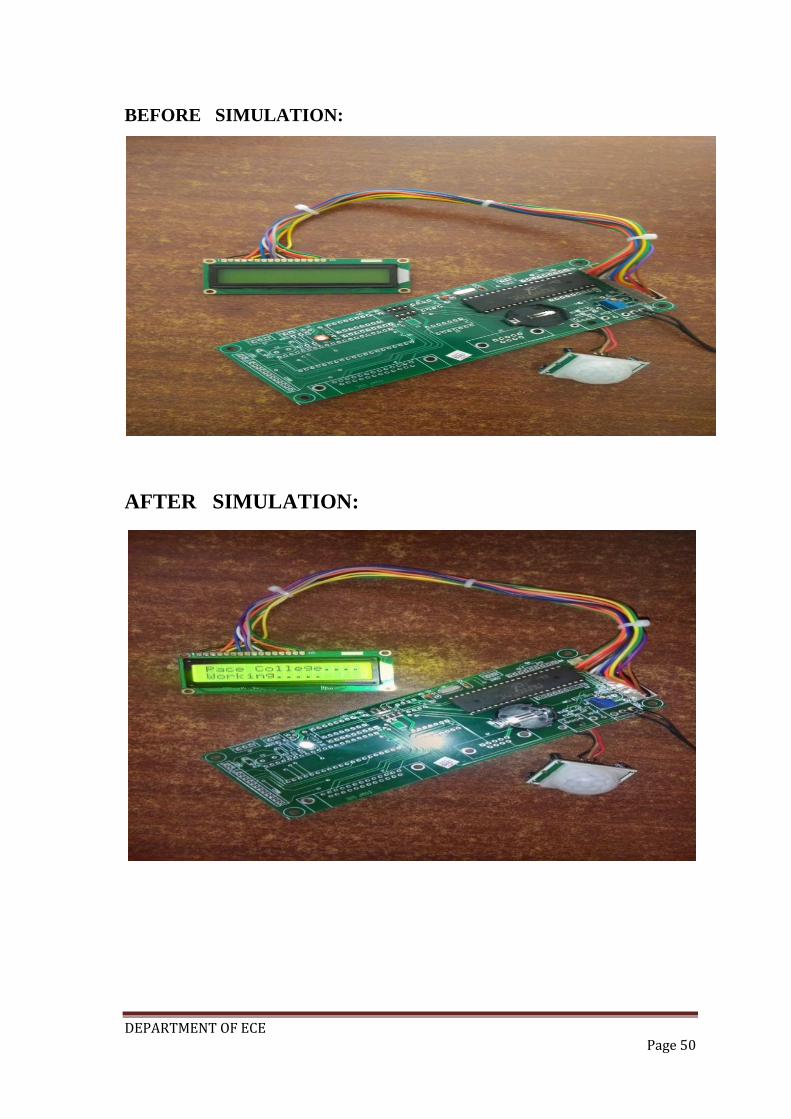
DEPARTMENT OF ECE Page 50
BEFORE SIMULATION:
AFTER SIMULATION:

DEPARTMENT OF ECE Page 51
CHAPTER 5
RESULTS AND CONCLUSION
5.1 RESULTS:
By observing all the above aspects of the power factor it is clear that power
factor is the most important part for the utility company as well as for the consumers.
Utility companies will be free from the power losses as well as the consumers are free
from low power factor penalty charges.
5.2 CONCLUSION & FUTURE RESULT:
The Power Factor is improved and the value becomes nearer to 0.9 to 0.95 by
installing suitably sized power capacitors into the circuit thus line losses are improved
and the efficiency of a plant increases [8]. By using this system the efficiency of the
system is highly improved. Precautions should be taken for over correction otherwise the
voltage and current increases due to which the power system or machine will not
remain stable and the life of capacitor bank decreases.
The automatic power factor correction by using capacitive load banks is
very efficient as it decreases the cost by reducing the power drawn from the supply.
As it operates automatically, no manpower is required and this Automated Power
factor Correction by using capacitive load banks can be used for the industries
purpose in the future. Further the project can be intensify by using thyristor control
switches in place of relay control so that contact pitting is avoided which is often
resulted by switching of capacitors due to flow of high in rush curve.

DEPARTMENT OF ECE Page 52
REFERENCES
[1] Jones, L. D.; Blackwell, D. ―Energy Saver Power Factor Controller for Synchronous.
Kaleem Gajangi and Vivya ansari, was proposed this concept and the website is
followed as ―http://www.aiktcdspace.org‖.
[2] Keith Harker (2014). ―Power System Commissioning and Maintenance practice.‖
London: Institution of Electrical Engineers.
[3] Stephen, J. C. (2015). ―Electric Machinery and Power System Fundamentals.‖ 3rd.ed.
United State of America: McGraw-Hill Companies, Inc.
[4] Barsoum, Nader (2016) ―Programming of PIC Micro-Controller for Power Factor
Correction‖ IEEE Conference on Modeling & Simulation, Pages:19-25.
[5] Rakendu Mandal; Sanjoy Kumar Basu; Asim Kar; Shyama Pada Chowdhury ―A
Microcomputer – Based Power Factor Controller‖, IEEE Transactions on Industrial
electronics, Volume: 41, Issue: 3, Pages:361–371.
[6] Jos Arrillaga, Neville R. Watson ―Power System Harmonics‖ 2nd.ed. Chichester:
JohnWiley.
[7] Ramasamy Natarajan. ―Power System Capacitors.‖ Boca Raton, FL: Taylor &
Francis.