A LOW-POWER METHODOLOGY FOR …staff.aub.edu.lb/~mm14/pdf/conferences/2011_ICEAC_mansour_low...A...
5
A LOW-POWER METHODOLOGY FOR CONFIGURABLE WIDE KOGGE-STONE ADDERS Zahi Moudallal Ibrahim Issa Mohammad Mansour Ali Chehab Ayman Kayssi Electrical and Computer Engineering Deparment American University of Beirut Beirut 1107 2020, Lebanon {zmm14, ihi02, mmansour, chehab, ayman}@aub.edu.lb ABSTRACT We propose a methodology to reconfigure a wide Kogge- Stone (KS) adder that is typically used in multimedia applications in order to minimize its power-delay product. The goal of the methodology is to enable the designer to select the best configuration to meet specifications in terms of power consumption, delay, and area. We measure the variations of these metrics by investigating several combinations of smaller KS adders connected in a ripple carry architecture. We test various adder combinations by performing HSPICE simulations in 90nm static CMOS. The results show that a designer can choose among different adder architectures to achieve different objectives. Index Terms— Kogge-Stone adder, Ripple-Carry adder, low power, high speed. 1. INTRODUCTION Integer addition is undoubtedly one of the most frequently used arithmetic operations in computer systems. Hence, adders affect significantly the performance of the system in terms of power and delay. There exists, however, a tradeoff between reducing power consumption and reducing the worst case delay. Therefore, researchers have developed several architectures to find the perfect balance. As power and energy constraints have become the more limiting factors in the design of computer systems, designers are shifting their attention to minimizing power and energy while meeting the delay constraints. In this paper, we propose a methodology that would allow a designer to choose the best configuration of a wide adder and we focus our study on Kogge-Stone adders coupled with a ripple-carry architecture. Since different applications and designs may assign different priorities and weights to power or delay, we present several alternatives for the implementation of a wide N-bit adder. The adder can be configured as a single block or it can be partitioned into P blocks connected in a carry ripple style with each block having a size of N/P bits. The corresponding data will aid designers to choose the preferred architecture according to the specifications they are targeting. As an example, a 1024- bit adder can be implemented as a single-block 1024-bit KS adder as sown in Figure 1, or it can be implemented, for instance, as 16 blocks of KS adders each with a size of 64 bits as shown in Figure 2. The paper is organized as follows: in section 2, we present a brief overview of previous work done related to low-power fast adders. We describe, in section 3, the architecture and the basic blocks of the KS adder. In addition, we include the different proposed implementation schemes for an N-bit adder (for N = 16 to 256). We summarize our results in section 4. Finally, we present a conclusion in section 5. 2. RELATED WORK Researchers have been extensively focusing on optimizing microprocessor performance by developing various adders’ architectures [1,2]. Most current high-performance microprocessors rely on parallel adders such as Brent-Kung [3], Sklansky [4] and Kogge-Stone adders [5,6]. The concept behind these adders is the depth of the look-ahead stages that they employ to compute the carry-in for each block. In other words, they compute the carry-in signals ahead of time instead of waiting for the carry bits to ripple through. This is maintained by generalizing the approach of bitwise generate and propagate signals to group generate and propagate signals. A group of bits generates a carry if its carry-out is true independently of the carry-in; and it propagates a carry if its carry-out is true when there is a carry-in. The mathematical recurrences of group generate and propagate signals for a group of bits spanning i to j are shown below followed with the equations for the base cases: !:! = !:! + !:! × !!!:! !:! = !:! × !!!:! !:! ≡ ! = ! × ! !:! = !" !:! ≡ ! = ! ⊕ ! !:! = 0
Transcript of A LOW-POWER METHODOLOGY FOR …staff.aub.edu.lb/~mm14/pdf/conferences/2011_ICEAC_mansour_low...A...

A LOW-POWER METHODOLOGY FOR CONFIGURABLE WIDE KOGGE-STONE ADDERS
Zahi Moudallal Ibrahim Issa Mohammad Mansour Ali Chehab Ayman Kayssi
Electrical and Computer Engineering Deparment American University of Beirut
Beirut 1107 2020, Lebanon {zmm14, ihi02, mmansour, chehab, ayman}@aub.edu.lb
ABSTRACT We propose a methodology to reconfigure a wide Kogge-Stone (KS) adder that is typically used in multimedia applications in order to minimize its power-delay product. The goal of the methodology is to enable the designer to select the best configuration to meet specifications in terms of power consumption, delay, and area. We measure the variations of these metrics by investigating several combinations of smaller KS adders connected in a ripple carry architecture. We test various adder combinations by performing HSPICE simulations in 90nm static CMOS. The results show that a designer can choose among different adder architectures to achieve different objectives.
Index Terms— Kogge-Stone adder, Ripple-Carry adder, low power, high speed.
1. INTRODUCTION Integer addition is undoubtedly one of the most frequently used arithmetic operations in computer systems. Hence, adders affect significantly the performance of the system in terms of power and delay. There exists, however, a tradeoff between reducing power consumption and reducing the worst case delay. Therefore, researchers have developed several architectures to find the perfect balance. As power and energy constraints have become the more limiting factors in the design of computer systems, designers are shifting their attention to minimizing power and energy while meeting the delay constraints. In this paper, we propose a methodology that would allow a designer to choose the best configuration of a wide adder and we focus our study on Kogge-Stone adders coupled with a ripple-carry architecture. Since different applications and designs may assign different priorities and weights to power or delay, we present several alternatives for the implementation of a wide N-bit adder. The adder can be configured as a single block or it can be partitioned into P blocks connected in a carry ripple style with each block having a size of N/P bits. The corresponding data will aid designers to choose the preferred architecture according to
the specifications they are targeting. As an example, a 1024-bit adder can be implemented as a single-block 1024-bit KS adder as sown in Figure 1, or it can be implemented, for instance, as 16 blocks of KS adders each with a size of 64 bits as shown in Figure 2. The paper is organized as follows: in section 2, we present a brief overview of previous work done related to low-power fast adders. We describe, in section 3, the architecture and the basic blocks of the KS adder. In addition, we include the different proposed implementation schemes for an N-bit adder (for N = 16 to 256). We summarize our results in section 4. Finally, we present a conclusion in section 5.
2. RELATED WORK Researchers have been extensively focusing on optimizing microprocessor performance by developing various adders’ architectures [1,2]. Most current high-performance microprocessors rely on parallel adders such as Brent-Kung [3], Sklansky [4] and Kogge-Stone adders [5,6]. The concept behind these adders is the depth of the look-ahead stages that they employ to compute the carry-in for each block. In other words, they compute the carry-in signals ahead of time instead of waiting for the carry bits to ripple through. This is maintained by generalizing the approach of bitwise generate and propagate signals to group generate and propagate signals. A group of bits generates a carry if its carry-out is true independently of the carry-in; and it propagates a carry if its carry-out is true when there is a carry-in. The mathematical recurrences of group generate and propagate signals for a group of bits spanning i to j are shown below followed with the equations for the base cases:
𝐺!:! = 𝐺!:! + 𝑃!:!×𝐺!!!:!
𝑃!:! = 𝑃!:!×𝑃!!!:!
𝐺!:! ≡ 𝐺! = 𝐴!×𝐵! 𝐺!:! = 𝐶!"
𝑃!:! ≡ 𝑃! = 𝐴! ⊕ 𝐵! 𝑃!:! = 0

Figure 1. Single block 1024-bit KS adder
Figure 2. 1024-bit adder configured as 16 blocks KS adders
(64-bit) in carry ripple style This approach opens up a new design space that provides various trade-offs in terms of logic stages, logic blocks per stage, fanout and wire tracks. Designing integer adders reduces to determining the number of carry-in signals that the adder is going to compute ahead of time. In other words, designing integer adders reduces to designing the tree of group PG logic presented in Figure 3. As a result, the sum is computed simply using XOR according to the formula:
𝑆! = 𝑃!⨁𝐺!!!:! Furthermore, the design space has been filled by combining different adder architectures to extend the trade-offs at the disposal of microprocessor designers. For example, the Han-Carlson architecture [7] is a combination of Kogge-Stone and Brent-Kung; the Knowles architecture [8] is a combination of Kogge-Stone and Sklansky, and the Ladner-Fischer architecture [9] is a combination of Skalnsky and Brent-Kung. We have discussed so far the group PG logic that computes the generate and propagate signals whereby it combines two previous stages and thus is called valency-2 cell. Higher valency tree adders could further reduce the delay of the adder [10].
Figure 3. Adder schematic [1]
It is well known that the total power dissipation of a typical CMOS circuit is given by [11]: 𝑃!"!#$ = (𝐶! ∙ 𝑉!!! + 𝑉!! ∙ 𝐼!"#$ ∙ 𝑡!") ∙ 𝑓!→! + 𝐼!"#$#%" ∙ 𝑉!!
The first term refers to the power consumed during charging and discharging of load capacitances while transistors are switching. The term (𝑓!→!) represents the frequency of transitions of a given output. The second term is the short-circuit power due to the current flowing from power supply to ground during transistor switching. The last term represents the static power due to leakage and static currents [12]. In this expression, the dominant term was historically the switching power, and hence lowering CL, VDD or 𝑓!→! leads to lower overall power consumption. Apart from reducing the delay of adders, Nagendra et al. provide in [13] a comprehensive and in-depth study of parallel adders and design tradeoffs that can reduce power consumption. The authors present a methodology to reduce short circuit power of an adder by proper sizing of transistors. Other studies were performed to reduce switching power by varying the supply voltage. Although reducing the supply voltage would provide a quadratic (or higher) improvement in power consumption, researchers have shown that it actually increases delay with severe effects at voltages close to the threshold voltage of transistors. As Liu and Svensson demonstrated in [14], reducing supply voltage may reduce power by about 40 times. On the other hand, as the supply voltage approaches the threshold voltage, the latter has to be scaled using advanced device technology and manufacturing methodologies. In this paper, our simulations are based on 90nm static CMOS technology for which leakage power is negligible compared to dynamic power. Moreover, we investigate the effectiveness of various combinations of Kogge-Stone blocks in a carry ripple architecture in reducing the load capacitance and hence minimizing power as well as maintaining low delay in order to widen the design space.
1024-bit Kogge-Stone Adder
(1 Block)
(1024)
A
A+B
CinCout
(1024)
B
(1024)
64-bit KSCinC1
64
B[0-63]
64
A[0-63]
64
S[0-63]
64-bit KSC15Cout
64
B[960-1023]
64
A[960-1023]
64
S[960-1023]
...
3. LOW-POWER ADDERS 3.1 Kogge-Stone Adder The Kogge-Stone adder is one of the fundamental tree adders that are widely used in high-performance processors. It generates the carry signals in O(log n) time, where n is the number of bits per input. The basic blocks of this adder are the “gray” cell and the “black” cell that compute the group generate and propagate signals. Figure 4 shows the logic schematic of valency-2 group PG blocks. A crucial observation based on the KS schematic shown in Figure 5 is that the KS adder employs log(n) stages of logic and a maximum of one (1) fanout at each stage. However, the wire tracks form the greatest loading of capacitance in this circuit, and hence the major delay and power factors.
Figure 4. Valency-2 black and gray cells [1]
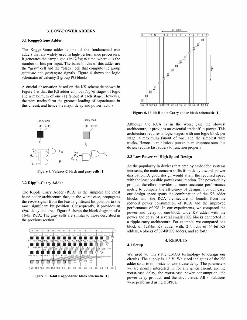
3.2 Ripple-Carry Adder The Ripple Carry Adder (RCA) is the simplest and most basic adder architecture that, in the worst case, propagates the carry signal from the least significant bit position to the most significant bit position. Consequently, it provides an O(n) delay and area. Figure 6 shows the block diagram of a 16-bit RCA. The gray cells are similar to those described in the previous section.
Figure 5. 16-bit Kogge-Stone block schematic [1]
Figure 6. 16-bit Ripple-Carry adder block schematic [1]
Although the RCA is in the worst case the slowest architecture, it provides an essential tradeoff in power. This architecture requires n logic stages, with one logic block per stage, a maximum fanout of one, and the simplest wire tracks. Hence, it minimizes power in microprocessors that do not require fast adders to function properly. 3.3 Low Power vs. High Speed Design As the popularity in devices that employ embedded systems increases, the main concern shifts from delay towards power dissipation. A good design would attain the required speed with the least possible power consumption. The power-delay product therefore provides a more accurate performance metric to compare the efficiency of designs. For our case, our design space spans the combination of the KS adder blocks with the RCA architecture to benefit from the reduced power consumption of RCA and the improved performance of KS. In our experiments, we compared the power and delay of one-block wide KS adder with the power and delay of several smaller KS blocks connected in a ripple carry architecture. For example, we compared one block of 128-bit KS adder with: 2 blocks of 64-bit KS adders, 4 blocks of 32-bit KS adders, and so forth.
4. RESULTS 4.1 Setup We used 90 nm static CMOS technology to design our circuits. The supply is 1.2 V. We sized the gates of the KS adder so as to minimize its worst-case delay. The parameters we are mainly interested in, for any given circuit, are the worst-case delay, the worst-case power consumption, the power-delay product, and the circuit area. All simulations were performed using HSPICE.

For the worst-case delay, we looked for the input vectors that activate the critical path, which is the path beginning at the least significant input bit and reaching the most significant sum bit and hence has the largest capacitive load. The corresponding transition was found to be the following: initially, both inputs are set to zeros, and so is the carry-in bit. Then, all bits of one of the inputs go from 0 to 1, and so does the carry-in. The most significant sum bit initially goes to 1, and then it switches back to 0 only when the generate signal propagates through all blocks (on the diagonal of Figure 5.) As for the worst-case power, it is obtained by the combination that switches the largest number of gates in the circuit: initially, all bits of both inputs and the carry-in are set to 1. Then, all bits of one of the inputs switch to 0. This flips all the generate signals from 1 to 0, all the propagate signals from 0 to 1, and all the output bits (except for carry-out) from 1 to 0. To estimate the area, we summed, over all transistors, the product of the width and the length of the transistor gate. Although this does not provide an accurate measure of the area, it is a rough approximation since we are interested in a relative size comparison of the different implementations of the wide adder. 4.2 Estimates To approximate the capacitances present in the circuit (especially along the long wires) we used the following estimates:
• Interconnect capacitance is 0.2 fF/µm.
• A two-input NAND (or NOR) gate is 1.5 µm x 1.5 µm in area (we used this size to estimate the length of the wires).
• There is a 1 µm spacing between successive levels
of logic.
• Moreover, for sizing purposes we estimated the input capacitance of a unit-sized inverter to be 2 fF.
4.3 Simulations Results To capture the delay, we measure the difference between the time the input crosses VDD/2 and the time the output last crosses VDD/2 (before stabilizing). The power values are obtained by measuring the average power over 100 ns simulation time, during which one transition occurs. For each N-bit adder, we performed simulations using both the KS architecture, and smaller blocks of KS adders
connected in ripple-carry architecture. We did not include, however, blocks with a number of inputs less than 4 bits. Table 1 shows a summary of our simulation results in terms of power and delay. Table 2 shows results related to the area of the adder circuits. The second column in these tables indicates the number of blocks used for each adder. For example at the intersection of the row labeled 8 and the column labeled 64 we have the results of a 64-bit adder made up of 8 blocks and hence each block is an 8-input adder. According to the results of Table 1, we can see that as we increase the number of blocks, the delay of the adder increases, except when comparing 2-block adders and 4-block adders. It seems that 4-block adders always outperform 2-block ones. Still, the single-block KS adder is always the fastest adder among all alternatives. Also, it is noticeable that the increase in delay is significant. Going from a single block to four increases the delay by a factor of at least 40% (for adders larger than 16 bits). When we compare a 1-block 256-bit adder with the 64-blocks we can observe an increase of 180% in delay. On the other hand, power decreases continuously as we increase the number of blocks. The decrease becomes more significant as the adders become larger and as the number of blocks increases. For the 16-bit adder, comparing one block to two shows a change of 9.3% in power, while for the 256-bit adder it shows a change of 31%. Also, for the 256-bit adder, comparing one block to 64 shows a much higher change of 75%. As for the power-delay product, there is no noticeable pattern for the shown variations. For a 64-bit adder, the 16 blocks of 4-bit adders have the smallest power-delay product. The 16 blocks of 8-bit adders show the lowest product for the 128-bit architecture, whereas the 32 blocks of 8-bit adders score the lowest for the 256-bit architecture. As a side note, cascading two blocks of KS adders proved useless since they are outperformed by four blocks in both aspects of delay and power (as well as area, see Table 2). The results of Table 2 show that the total area decreases when we increase the number of blocks per adder. The change is obvious since for the 128-bit adder, the area decreases by 18% when a single block is replaced by 2, 43% when it is replaced by 8 blocks, and 59% when replaced by 32 blocks. The results are similar for the 256-bit adder whereby replacing a single block by 32 blocks reduces the area by 61% and by 67% when 64 blocks are used.

Table 1. Simulation Results (Delay and Power)
N-bit adders
16 32 64 128 256
Del
ay (p
sec)
1 369.98 469.4 693.11 1010.6 1528.7 2 472.85 740.09 1014 1501.9 2272.2 4 417.77 655.68 1014 1449 2242.2 8 674.67 1021.6 1561.9 2320.1
16 1188.9 1754.3 2657.2 32 2217.5 3219.3 64 4275.3
Pow
er (µ
W)
1 8.0272 21.412 57.97 160.12 466.18 2 7.282 19.4 51.33 117.45 321.21 4 6.267 16.43 42.33 111.52 283.61 8 13.64 34.73 88.193 231.97
16 28.41 71.364 179.93 32 57.97 144.62 64 117.08
Pow
er-D
elay
Pr
oduc
t (fJ
)
1 2.970 10.051 40.180 161.82 712.65 2 3.443 14.358 52.049 176.4 729.85 4 2.618 10.773 42.923 161.59 635.91 8 9.202 35.480 137.75 538.19
16 33.777 125.19 478.11 32 128.55 465.58 64 500.55
Table 2. Total Transistor W×L Areas
N-bit adders
16 32 64 128 256
W×L
Are
as
(µm
2 )
1 22.524 54.068 130.51 317.97 781.45 2 19.008 45.048 108.14 261.03 635.93 4 16.128 38.016 90.095 216.27 522.06 8 32.256 76.032 180.19 432.54
16 64.512 152.06 360.38 32 129.02 304.13 64 258.05
5. CONCLUSIONS AND FUTURE WORK
In this paper, we compared different implementations of an N-bit wide adder using the Kogge-Stone and the Ripple-Carry architectures. The comparison was based on several criteria including: worst-case delay, worst-case power, power-delay product, and area. We performed our simulations on 16, 32, 64, 128, and 256-bit adders. We thus offered different alternatives (each possibly outperforming the others in one aspect but not in all) for designers who are currently facing conflicting objectives of minimizing both power and delay. In the process, we found that two cascaded
adders (in ripple architecture) are always outperformed by four cascaded smaller adders. Since the Kogge-Stone adder shows a well defined pattern in its architecture, we believe that our results can be generalized for larger adders such as 512 bits and 1024 bits. Future work will include extending the simulation results to 1024-bit adders, designing the layout and extracting the parasitics for more accurate simulation results, in addition to optimizing the structure of other high-speed adders.
ACKNOWLEDGMENTS This work was supported by the Intel-KACST Middle East Energy Efficiency Research (MER).
REFERENCES [1] D. Harris, “A Taxonomy of Parallel Prefix Networks,” in Proc. 37th Asilomar Conf. Signals Systems and Computers, pp. 2213–7, 2003. [2] K.Vitoroulis, A.J Al-Khalili, “Performance of Parallel Prefix Adders implemented with FPGA technology”, IEEE Northeast Workshop on Circuits and Systems, 2007. NEWCAS 2007, pp. 498 – 501, 5-8 Aug. 2007. [3] R. Brent and H. Kung, “A regular layout for parallel adders,” IEEE Trans. Computers. vol. G31, no. 3, pp. 260-264, March 1982. [4] J. Sklansky, “Conditional-sum addition logic,” IRE Trans. Electronic Computers, Vol. EC-9, pp. 226-231, June 1960. [5] P. Kogge and H. Stone, “A parallel algorithm for the efficient solution of a general class of recurrence relations,” IEEE Trans. Computers, vol. C- 22, no. 8 , pp. 786-793, Aug. 1973. [6] T. Lynch and E. E. Swartzlander, “A Spanning Tree Carry Lookahead Adder,” IEEE Trans.Comput., 41(8):931–939,August 1992. [7] T. Han and D. A. Carlson, “Fast Area-Efficient VLSI Adders,” in Proc. 8th Symp. Comput. Arithmetic, 1987, pp. 49-56 [8] S. Knowles, “A Family of Adders,” in Proc. 15th IEEE Symp. Comp. Arith., pp. 277-281, June 2001. [9] R. Ladner and M. Fischer, “Parallel Prefix Computation,” J. ACM, vol. 27, no. 4, Oct. 1980. [10] Neil H.E. Weste and Kamran Eshraghian, Principles of CMOS VLSI Design, A Systems Perspective, Second Edition, Addison-Wesley Publishing Company, 1993, pp. 436-440 and 447-451. [11] J. Rabaey, Digital Integrated Circuits—A Design Perspective. Englewood Cliffs, NJ: Prentice-Hall, 1996, pp. 219-221. [12] A.M. Shams, T.K. Darwish, M.A. Bayoumi, “Performance Analysis of Low-Power 1-bit CMOS Full Adder Cells,” IEEE Transactions on VLSI Systems, vol. 10, pp. 20–29, Jan. 2002. [13] C.N. Nagendra, M.J. Irwin, R.M. Owens, “Area-Time-Power Tradeoffs in Parallel Adders,” IEEE Transactions on Circuits and Systems-II: Analog and Digital Signal Processing, vol. 43, no. 10, Oct. 1996. [14] D. Liu and C. Svensson “Trading speed for low power by choice of supply and threshold voltages,” IEEE Journal of Solid-State Circuits, vol. 28. pp. 10-17, Jan. 1993.