A Logic Built-in Self-test architecture that reuses ... · CHAPTER 5 - CASE STUDY ... Another...
64
Federal University of Pernambuco Informatics Center Post-graduation in Computer Science A Logic Built-in Self-test architecture that reuses manufacturing compressed scan test patterns Diogo José Costa Alves MASTER PROMOTION Recife March 10, 2009 Federal University of Pernambuco
Transcript of A Logic Built-in Self-test architecture that reuses ... · CHAPTER 5 - CASE STUDY ... Another...

Federal University of Pernambuco
Informatics Center
Post-graduation in Computer Science
A Logic Built-in Self-test architecture that reuses manufacturing compressed scan test patterns
Diogo José Costa Alves
MASTER PROMOTION
Recife March 10, 2009
Federal University of Pernambuco

2
Informatics Center
Diogo José Costa Alves
A Logic Built-in Self-test architecture that reuses manufacturing compressed scan test patterns
Submitted to the Computer Science Post-graduation Program in Partial Fulfillment of the Requirements for the Degree of Master Computer Science at the Informatics Center from the Federal University of Pernambuco
Thesis Supervisor: Ph.D. Edna Natividade da Silva Barros
Recife March 10, 2009

3
Acknowledgments First and foremost, I would like to thank my family. Throughout all my endeavors, your love, support, guidance, and endless patience have been truly inspirational—“thanks” will never suffice. In special my wife, Helena, whose patient and tenderness enabled me to complete this work. I would like to thank Mrs. Edna Barros my advisor. She was very patient with me and allowed me to pursue my own theories through my experiments. I am very grateful to all people who contributed to this project.

4
Abstract The claim for new functionalities regarding the improvement of dependability of electronic systems and also the need for managing the time spent during test make the Built-in-Self-Test mechanism (BIST) a promising feature to be integrate in current IC flows. There are a lot of types of BIST: Memories BIST, Logical BIST(LBIST) and also some mechanisms used to test analog parts of circuit. Traditional LBIST uses on-chip hardware to generate all test patterns with a pseudo-random-pattern-generator (PRPG) and analyze the output response. Generating all test stimuli implies in a sacrifices of test application time, which can be acceptable for some small systems to perform self-test during boot up but could become a negative aspect when testing System-on-chip (SOC) ICs. The current IC development flow insert scan chains and generates automatically scan tests patterns to achieve high fault coverage for manufacturing test. Scan data compression techniques have proven to be very useful for reducing test cost while reducing test data volume and test application time. This work proposes the reuse of compressed scan test patterns used during manufacturing test to implement a LBIST with the goal of testing the circuit when it is already in field. The proposed LBIST mechanism aims to uncover defects that could occur due to the wear out of the circuit. A scan test pattern based LBIST development flow is proposed and validated in a real word SoC testcase. Key words: LBIST, compressed test patterns, self-test.

5
Resumo Estendido Testar é uma das etapas finais do ciclo de produção de um circuito integrado (CI) e é de fundamental importância para garantir que os clientes terão CIs que funcionem. Sendo essa uma etapa importante em termos de influenciar a satisfação do cliente, o teste com o passar dos anos tem tido um papel proeminente na concepção global dos CIs. Design for Test é o nome dado para as técnicas de concepção que acrescentam características de testabilidade no produto de hardware microeletrônico. A idéia é que as funcionalidades adicionadas tornam mais fáceis desenvolver e aplicar testes durante a fabricação do circuito-integrado projetado. O modo convencional de testar o CI durante a manufatura é usar máquinas automáticas que alimentam as entradas e checam as respostas da saída utilizando todos os pinos do circuito-integrado. Por isso esse procedimento não é aplicável quando o CI já está soldado placa final do produto. Um caminho alternativo para suportar o teste co CI quando este já está soldado na placa final do produto é reduzir o número de pinos de entrada/saída necessários para executar o teste. Isso é feito ao inserir dentro do CI um conjunto extra de lógica digital responsável por executar um auto-teste. Esse é o conceito principal de Built-in self-test (BIST). Logic BIST (LBIST) é o mecanismo BIST usado para testar os módulos digitais do circuito. A arquitetura tradicional LBIST gera dentro do chip todos os padrões de teste utilizando a um gerador-pseudo-aleatório-de-padrões (pseudo-random-pattern-generator PRPG) e analisa a resposta de saída. Eliminando assim a necessidade de armazenar informação na máquina de teste e sendo útil para executar o auto-teste em campo quando não há acesso a máquina de teste. O uso do PRPG para gerar todos os estímulos de teste implica também em um sacrifício no tempo de aplicação do teste, que pode ser aceitável para executar auto-teste em pequenos CI durante a inicialização do sistema, mas pode tornar-se um aspecto negativo quanto testando sistemas maiores. O fluxo atual de desenvolvimento de CIs insere estruturas que facilitam o teste e gera automaticamente padrões de teste para atingir uma alta cobertura de falhas para parte de lógica digital durante o teste de manufatura. Técnicas de compressão de padrões de teste têm provado úteis em reduzir o custo do teste ao mesmo tempo em que reduz o volume de dados e o tempo de aplicação do teste. Esse trabalho propõe uma arquitetura que reusa padrões testes usados durante o teste de manufatura para implementar um

6
mecanismo LBIST. O mecanismo LBIST proposto visa descobrir defeitos no quando este já está em campo. Uma estratégia de desenvolvimento é também proposta e validada com um caso de teste.

7
Nomenclature ATE Automated test equipment ATPG Automatic Test Pattern Generation BIST Built-in self-test BSR Boundary Scan Registers CUT Circuit under test DFT Design for Test EDA Electronic Design Automation HDL Hardware description Language IC Integrated circuit LBIST Logic Built-in self-test MISR Multiple input shift register OCC On-chip-clock PRPG Pseudo Random Pattern Generator RPR Random-pattern-resistant faults RTL Register Transfer Level SAF Stuck-at fault model SNPS TC Synopsys Test coverage SOC System-on-chip STIL Standard Test Interface Language TAP Test Access Port TAT Total Application Time TCK TAP clock port TCR Test Control Registers TDV Total Data Volume TMC Test mode control register TSR Test Status Registers

8
Contents
LIST OF TABLES ............................................................................................... 9
CHAPTER 1 - INTRODUCTION ...................................................................... 10
CHAPTER 2 – BACKGROUND ...................................................................... 13
CHAPTER 3 – RELATED WORKS ................................................................ 26
CHAPTER 4 - GENERAL STRATEGY FOR IMPLEMENTING A SCAN TEST PATTERN BASED LBIST. ................................................................... 35
CHAPTER 5 - CASE STUDY .......................................................................... 44
CHAPTER 6 - CONCLUSIONS ....................................................................... 53
BIBLIOGRAPHY ............................................................................................... 55
APPENDIX A - GENERATING MOST EFFICIENT TEST PATTERNS ...... 58
APPENDIX B - TAP MODIFICATIONS .......................................................... 61

9
List of Figures Figure 1 - Digital IC Development Flow ...................................................................... 13 Figure 2 - Automatic test equipment ........................................................................... 15 Figure 3 - Scan chains in a logic design ..................................................................... 16 Figure 4 - Test pattern application procedure ............................................................ 17 Figure 5 - Test patterns generation flow ..................................................................... 19 Figure 6 - Adaptive Scan architecture ......................................................................... 20 Figure 7 - General LBIST scheme ............................................................................... 22 Figure 8 – STUMPS architecture ................................................................................. 23 Figure 9 - Hybrid patterns LBIST architecture ........................................................... 27 Figure 10 - Bit-flipping Deterministic LBIST architecture ......................................... 28 Figure 11 - BFF generation procedure ........................................................................ 29 Figure 12 - OpenSPARC with CASP support ............................................................ 31 Figure 13 - CASP procedure overview [6] .................................................................. 32 Figure 14 - Compressed scan pattern LBIST architecture ...................................... 36 Figure 15 - Autonomous LBIST execution flow ......................................................... 37 Figure 16 - Improving LBIST test coverage with multiples boot ups ...................... 38 Figure 17 - Host computer – JTAG/TAP control flow ............................................... 39 Figure 18 - Scan test pattern LBIST in Digital IC development flow ...................... 40 Figure 19 - Scan test patterns based LBIST development flow .............................. 41 Figure 20 - Isolation between LBIST scan chains and CUT scan chains ............. 42 Figure 21 - Test protocol configuration for generating pattern for LBIST .............. 42 Figure 22 - Testcase overview ..................................................................................... 44 Figure 23- Test data volume for compressed and non-compressed test modes . 45 Figure 24 - Test data volume reduction for different test coverage ........................ 45 Figure 25 - LBIST controller internal architecture ..................................................... 48 Figure 26 - Implemented architecture ......................................................................... 50 Figure 27 - TCR static bit description .......................................................................... 63 Figure 28 - TCR connections with LBIST muxes ...................................................... 63 Figure 29 - Connections between TCR and module in charge of pulsing clock ... 64 Figure 30 - TSR description .......................................................................................... 64
List of Tables Table 1 - Summary of presented works ...................................................................... 33 Table 2 - Occupied space on program memory ........................................................ 46 Table 3 - Test application time ..................................................................................... 46 Table 4 - Result summary ............................................................................................. 50 Table 5 - ATPG experiments summary ...................................................................... 59 Table 6 - Proposed modification in TCR+TSR .......................................................... 61

10
Chapter 1 - Introduction Testing is one of the final stages in the production cycle of integrated circuits (IC) and is of fundamental importance to assure that customers will get working IC units. Being such an important stage in terms of influencing customer satisfaction, test has over the years taken a very prominent role in the overall IC design and test cycle. Design for Test is a name for design techniques that add some testability features to a microelectronic hardware product design. The premise of the added features is that they make it easier to develop and apply manufacturing tests for the designed hardware. The purpose of manufacturing tests is to assure that the product hardware contains no defects that could, adversely affect product’s correct functioning. The conventional way of test IC during manufacturing is to use automated test equipment that supplies the input stimuli and check the output responses using all pins of IC. Therefore this procedure is not applicable when the IC is already soldered in the final product board. Creating more robust designs with self-checking and self-healing mechanisms is the main motivation to enabling the IC test while it is already in production board [1][6][18][22]. An alternative way to support testing IC when it is already soldered in the final product board is to reduce the number of needed pins to perform test. This is done by inserting inside the IC some extra-logic in charge of testing itself. This is the main concept of Built-in self-test (BIST). A built-in self-test mechanism permits an IC to test itself. Engineers use BIST when it is the cheaper way to test the IC during manufacturing and also when an IC has to have auto-diagnosis feature. The claim for new functionalities regarding the improvement of dependability of electronic systems and also the need for managing the time spent during test make the BIST mechanism a promising feature to be integrated in current IC flows. There are a lot of types of BIST: Memory BIST to test memories, Logical BIST (LBIST) to test circuit digital parts and also some mechanisms used to test analog parts of circuit [1][22][23]. Traditional LBIST uses on-chip hardware to generate all test patterns with a pseudo-random-pattern-generator (PRPG) and analyzes the output response. Thus eliminating the need of tester storage and being useful for performing self-test in the field when there is no access to a tester. Despite the lack of need of storing test information, the use of PRPG is not the most suitable to address some fault models like transition and bridging , even when using only stuck-at fault model the

11
insertion of additional test points are required to achieve high fault coverage [8]. The use of PRPG to generate all test stimuli implies also in an increase of test application time (TAT), which can be acceptable for small systems to perform self-test during boot up, but could become a negative aspect when testing System-on-chip (SOC). Also when the system is checked periodically to test the IC already in field against defects that could occur due to the wear out of the circuit the TAT can become critical and impacts negatively in system overall downtime. Another problem of using a test architecture with PRPG is the process of calculating the achieved system test coverage. The fault simulation procedure used to verify which faults are exercised by a sequence of PRPG stimuli is a very computer intensive task. Performing fault simulation of whole PRPG stimuli sequence for today SoC is just not possible. In consequence the use PRPG in a LBIST implicates in not knowing the final test coverage for SoC designs. This work proposes the reuse of compressed scan test patterns used during manufacturing test to implement a LBIST with the goal of testing the circuit when it is already in field. The proposed LBIST mechanism aims to uncover defects that could occur due to the wear out of the circuit. The current IC development flow insert scan chains and generates automatically scan tests patterns (ATPG) to achieve with high fault coverage for digital logic part during manufacturing test. The reuse of scan test patterns means that the test coverage is already known during ATPG. Also the test application time when using a deterministic set of scan test pattern is shorter than achieving the same coverage of using a pseudo-random stimuli sequence from traditional LBIST approach. This work proposes an architecture that reuses test scan compressed test patterns used during manufacturing test to implement a LBIST. A scan test pattern based LBIST development flow is proposed and validated in a real world SoC testcase. This work is organized in six chapters. The next chapter introduces some important concepts to understand and contextualize the contributions of the proposed work. Chapter three analyses related works concerning Logic BIST architectures. Chapter four presents the proposed LBIST development flow and architecture, which uses compressed patterns stored inside an internal

12
memory to supply internal scan chains instead using PRPG as in traditional LBIST approach. Chapter five applies the proposed strategy in a real world design to discuss the implementation challenges of the scan test pattern based LBIST. Finally the last chapter discusses how the main challenges were addressed, points how it could be improved and summarize the conclusions of the work.

13
Chapter 2 – Background This chapter introduces some important concepts to understand and contextualize the contributions of the proposed work.
Digital IC Development Flow The process of development of Digital IC, presented in Figure 1, starts with Design Specification where the product is described in terms of functionality, performance, operating conditions, silicon area, testability, fault coverage and other criteria that affect the design. In sequence in the Design Partition phase a Top-down effort defines product architecture and partition the hardware blocks which will be implemented.
Figure 1 - Digital IC Development Flow
During Front End part of flow in Design Entry, the hardware blocks are described in a Hardware description language (HDL), like VHDL and

14
Verilog. After that, each functionality block is verified by simulation. And then the whole system is integrated and verified again. In sequence in Logic synthesis an EDA tool is used to create an optimal netlist of design satisfying area and performance constraints according product specifications and IC process technology. The functionality of synthesized description is checked against the HDL description. During DFT Insertion some additional logic circuit is incorporated into the IC to make easier testing the circuit during fabrication. After that, test patterns are generated in ATPG phase according to the product test quality requirements. An important point here is that test patterns can be generated just after DFT Insertion but in fact these final test patterns are generated after Backend work. Small modifications in the design are commons during Backend work. Those modifications have an unpredictable impact in test coverage. In order to not impact the final test quality the test patterns should be generated again. The proposed work is mainly involved in these two parts of flow: DFT Insertion and ATPG generation. Continuing the flow, the Back-end part starts with Placement and Route activities. The placement and routing step arranges the cells on the IC and connects their signal paths. After that, the physical layout of a design must be checked to verify that constraints on interconnection paths widths, overlaps, and separations are satisfied. Electrical rules are checked to verify that fanout constraints are met and that signal integrity is not compromised by electrical crosstalk and power-grid drop. The parasitic capacitance induced by the layout is extracted by EDA tools and then used to produce a more accurate verification of the electrical characteristics and time performance of the design. The Post-Layout Verification the timing and low-power constraints are checked to confirm that the design will function at the specified clock speed and power consumption constraints. After all design constraints have been satisfied, the project is ready for the Design Sign-Off. At this point the IC is ready for being produced.

15
Manufacturing testing flow Quality aspect is very important and even a low number of defective devices are critical for company image at customers. Because it the manufacturing test is important. Testing a semiconductor device is checking that the device meets its electrical specification. Manufacturing test is done on each circuit, where the device is accepted or rejected. The main cost component in manufacturing test phase is the time required to test the device. The circuit under test (CUT) must be tested in a time frame of seconds. An automated test equipment (ATE) is used to quickly test the integrated circuit. Figure 2 shows the conventional way of testing using an equipment to generate stimuli and check the IC responses.
Figure 2 - Automatic test equipment
Design for Test or Design for Testability (DFT) encompasses all efforts directed to ensure that the circuit is testable at less time possible to deliver working pieces to the customer and avoid packaging bad circuits. During DFT Insertion small logic blocks are added in the design to improve the design controllability and observability during manufacturing test. Controllability and Observability are key concepts for DFT. Controllability is the ability to set or reset each internal node in

16
the design while Observability is the ability to observe any circuit node’s state. Some of features added in circuit to improve testability of system are:
• Boundary scan for testing chip pads; • Scan chains for testing digital logic; • Built-in Self-test (BIST) for enabling self-test feature in specific
parts of design, such memory arrays, digital or analog blocks. We will concentrate our background overview in Scan chains insertion technique and LBIST which is a BIST approach targeted to digital circuits.
Scan chains insertion Scan chains insertion it the DFT technique used to provide a simple way to set and observe every flip-flop in an integrated circuit. When the IC is configured in test mode, every flip-flop in the design is connected into a long shift register, one input pin provides the data to this chain, and one output pin is connected to the output of the chain. Then using a clock signal, a test pattern can be entered into the chain of flips flops, and the state of every flip flop can be read out. Figure 3 shows a general view of how scan chains are arranged in a circuit.
Figure 3 - Scan chains in a logic design
The procedure of scan test pattern application, illustrated in Figure 4, is very important for the well understanding of this work. A scan test pattern is usually applied in the following manner:

17
1. Set up the scan chain configuration. Scan enable signal activated. 2. Shift values into the active scan chains. 3. Exit the scan configuration. Scan enable signal deactivated. 4. Apply stimulus to the inputs and measure the outputs. 5. Capture the test circuit response in flip-flops. 6. Set up the scan chain configuration. Scan enable signal activated. 7. Shift values out of the active scan chains. 8. Exit the scan configuration.
Figure 4 - Test pattern application procedure
The time necessary to apply one pattern can be calculated with:
1. Time to shift in one test pattern (Number of flip-flops in scan chain * tester clock period);
2. Capture clock (1 tester clock period); 3. Time to shift out the result Number of flip-flops in scan chain *
tester clock period); As we can see, the test application time (TAT) depends clearly on the length of scan chain. Another important metric is the test data volume (TDV) which represents the total of data stored in the tester. TAT and TDV are defined as:
odTesterPerilenghtchainlengthchainnsATPGpatterTAT *]_max_)1_(max_*[# ++=chainsscanexternallengthchainnsATPGpatterTDV __*#_max_*#=

18
Where: #ATPGpattern = Number of scan test patterns. Max_chain_length = Length of longest scan chain. TesterPeriod = Clock period used during test. #External_scan_chains = Number of pins used during test.
Scan test patterns generation Manufacturing testing verifies that the IC does not have manufacturing defects by focusing on circuit structure rather than functional on the behavior. A manufacturing defect has a logical effect on the circuit behavior. A signal shorted to power appears to be permanently high. A signal shorted to ground appears to be permanently low. Many of these manufacturing defects can be represented using the industry-standard “stuck-at” fault model. The stuck-at-0 model represents a signal that is permanently low regardless of the other signals that normally control the node. The stuck-at-1 model represents a signal that is permanently high regardless of the other signals that normally control the node. The node of a stuck-at fault must be controllable and observable for the fault to be detected. To detect a stuck-at fault on a target node, the designer must do the following:
• Control the target node to the opposite of the stuck-at value by applying data at the primary inputs.
• Make the node’s fault effect observable by controlling the value at all other nodes affecting the output response, so the targeted node is the active node.
Automatic-test-patterns-generation (ATPG) generates scan test patterns that provide high test coverage for digital logic designs. The ATPG tool used in this work was Synopsys TetraMAX [13] tool. TetraMAX uses deterministic techniques to generate test patterns for stuck-at faults. During deterministic pattern generation, see Figure 5, the tool uses a pattern generation algorithm based on path-sensitivity concepts to generate a test vector that detects a specific fault in the design. After generating a vector, the tool fault-simulates the vector to determine the complete set of faults detected by the vector. Test pattern generation continues until all faults either have been detected or have been identified as undetectable by the algorithm.

19
Figure 5 - Test patterns generation flow
One definition of a design’s testability is the extent to which that design can be tested for the presence of manufacturing defects, as represented by the single stuck-at fault model. Using this definition, the metric used to measure testability is test coverage. Test coverage gives the most meaningful measure of test pattern quality and is the default coverage reported in the fault summary report. Test coverage is defined as the percentage of detected faults out of detectable faults, as follows:
100*det sectedFaultUnAllFaultsultsDetectedFa
geTestCovera−
=
Scan compression schemes The increasing cost of test and design complexity introduces the need for reducing pin counts and scan pattern data. The proposed work makes use of already available compression schemes. The Adaptive Scan is a test compression scheme available at Synopsys DFT Compiler [14] tool. It provides a simple scan based flow with minimal area and test pin count overhead. The key concept to reduce the Test Application Time is to augment the number of internal scan chains thus reducing their length and the time required to shift in data. The amount of available primary scan in/out ports clearly limits the parallelism of scan chains. To overcome this limitation, Figure 6 proposes an architecture that relies on a very high number of internal scan chains and uses “decompressor” logic to generate scan-in data for all the internal scan chains, starting from the data loaded through the few primary scan input pins. A “compressor” logic is used to compact the scan-out data produced by the internal scan chains and unload the compacted data through the few primary scan out pins.
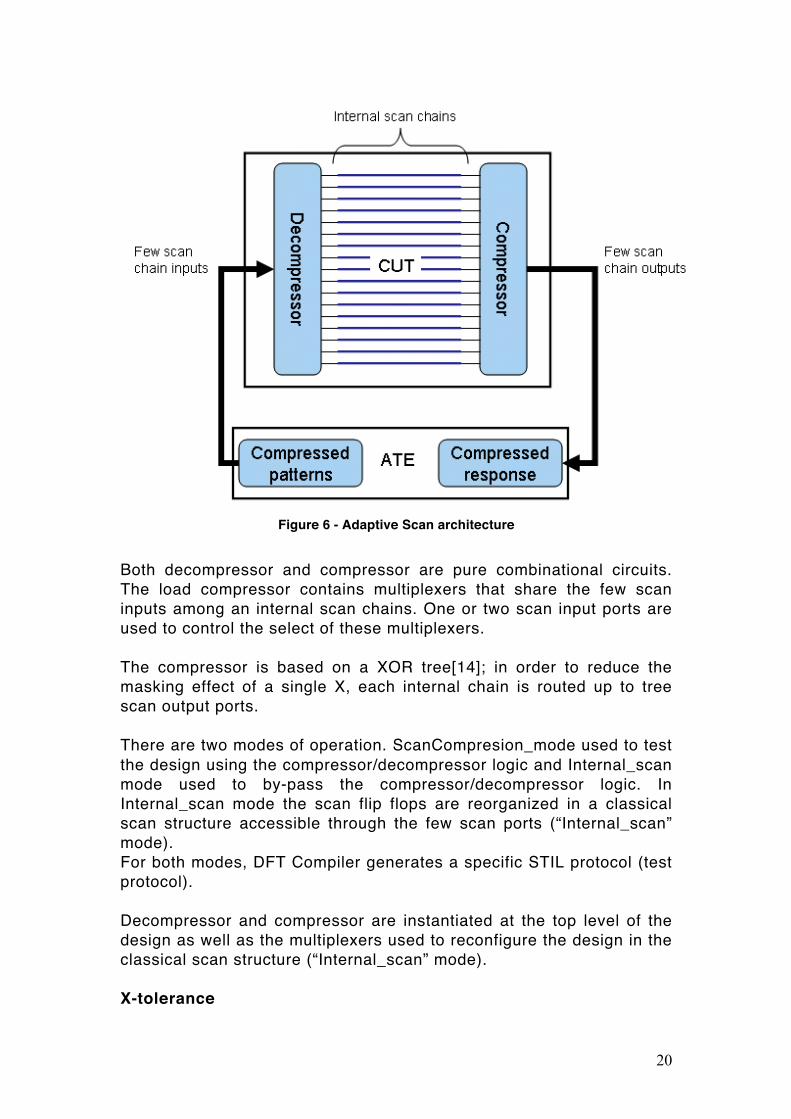
20
Figure 6 - Adaptive Scan architecture
Both decompressor and compressor are pure combinational circuits. The load compressor contains multiplexers that share the few scan inputs among an internal scan chains. One or two scan input ports are used to control the select of these multiplexers. The compressor is based on a XOR tree[14]; in order to reduce the masking effect of a single X, each internal chain is routed up to tree scan output ports. There are two modes of operation. ScanCompresion_mode used to test the design using the compressor/decompressor logic and Internal_scan mode used to by-pass the compressor/decompressor logic. In Internal_scan mode the scan flip flops are reorganized in a classical scan structure accessible through the few scan ports (“Internal_scan” mode). For both modes, DFT Compiler generates a specific STIL protocol (test protocol). Decompressor and compressor are instantiated at the top level of the design as well as the multiplexers used to reconfigure the design in the classical scan structure (“Internal_scan” mode). X-tolerance

21
Some compression architectures are don’t care (X) intolerant because use a multiple-input-shift-register (MISR) to compact the stream of output. In some test architectures a MISR is used to generate a signature of scan-chains outputs. If the tested block is operating free of defects the MISR would generate a single correct signature. Any disturb in scan chain outputs impacts the generation of an incorrect signature. Due to the fact that the signature is sensitive to any output change, a single X can corrupt the signature if it is propagated to the MISR. Synopsys DFT MAX [14] can implement an additional XOR-based compactor to avoid X-propagation to scan outputs, so making it possible the use of a MISR. Managing X-propagation in complex designs is unavoidable. X-sources [26] can be manifold, very often due to:
- Memories in combinational ATPG (especially when internal bypass is unusable)
- Memory contentions - Legacy IP cores - Non-digital blocks - Timing exceptions - Disturbed clock grouping
To minimize X-propagation a compression flow has been made available in DFT Compiler which provides 100% X-tolerance. This flow integrates test logic which allows to selectively observing internal chains on scan output ports directly, removing any influence caused by the presence of an XOR-tree. X-blocking logic is automatically activated during ATPG on a per-shift basis whenever the presence of one or more “Xs” prevents a target fault from being detected.
Logic Built-in Self-test The conventional way of test is to put the IC in an ATE, to generate test stimuli and check the IC responses. In this case all PINS are used, therefore this procedure is not applicable when the IC is soldered in final product board. An alternative way to support testing IC when it is already soldered on final product board is to reduce the number of needed pins to perform test. It could be done by inserting inside the IC some extra-logic in charge of testing the circuit itself. This approach, illustrated in Figure 7 uses the main concept of Logic BIST (LBIST) which consists of a self test mechanism for digital circuits.

22
Figure 7 - General LBIST scheme
The LBIST architecture most commonly used is the STUMPS [1] architecture, see Figure 8, which uses a pseudo-random pattern generator/linear feedback shift register (PRPG/LFSR) to generate the inputs to the device's internal scan chain, initiate a functional cycle to capture the response of the device, and then compress the captured response into a MISR. The output of the MISR is called test signature and any corruption in output test signature indicates structural defect in the device.

23
Figure 8 – STUMPS architecture
The Stumps LBIST architecture shown in Figure 8 includes an LBIST controller, a PRPG/LFSR register, a MISR register, scan chains, and a simple combinational logic between the scan chains, the PRPG and the MISR. Given an initial state the LFSR generates a predictable but randomized sequence of test patterns. The logic stimulus that is derived from these states is shifted into the scan channels through a spreader network that is usually constructed of XORs. The values in the scan channels represent the stimulus portion of the test pattern. During one or more clock pulses, the response of the circuitry to the test pattern stimulus is captured in the scan channels. The captured response is then shifted from the scan channels into another state machine, the MISR. After the test procedure is applied-provided the circuitry was free of defects-the MISR that was initialized to a known state has an expected final state, predicted by simulation. After some test time a signature will be provided by tested IC and compared with a signature stored off-chip. This mechanism can be used when the system is already in-field for in periodic system checking for failures and implementing system auto-repair capabilities. The objective of these tests is to uncover defects that could occur due to the wear out of the circuit. However achieving stuck-at high fault coverage with this mechanism needs a considerable overhead due to the existence of random-pattern-

24
resistant (RPR) faults. RPR faults [25] are faults that are not detectable by PRPG test patterns due their linear dependency and auto-correlation. The main alternatives to address RPR faults are the insertion of extra test points [15][16] or the use of deterministic information stored outside chip [17]. As storing some information outside chip seems to make the LBIST less Built-in and depending of amount of required data this can become a problem. The use of additional test points increase controllability and observability thus making the design more random-pattern testable. The undesirable aspect of test point insertion is that it adds delay along functional paths [3]. Despite of the no need of storing test information outside chip provided by STUMPS approach, the generation of all test patterns during LBIST test procedure implies also increases of TAT. The time to generate all test patterns can be acceptable for some ICs to perform the test during boot up but could become a negative aspect for testing some big SoCs. Also when system is checked periodically this fact can become critical and can impact negatively the system availability. Another problem is the LBIST test effectiveness when using a PRPG. The test coverage of LBIST using PRPG can be calculated through simulation of whole circuit for each generated pattern. Synopsys TetraMAX together with VCS Synopsys Verilog simulator have been already used for validating a small count of scan test patterns [24]. However the problem is that the PRPG generates a huge number of patterns to achieve the same test coverage achievable by small number of determinist pattern from ATPG. The huge number of test patterns makes the measurement of test coverage performed by simulation a very costly operation. The time necessary for simulating the circuit to measure the test coverage make this approach impracticable for today commercial SoC. This work proposes the reuse of compressed scan test patterns used during manufacturing test to implement a LBIST with the target of testing the circuit when it is already in field. The proposed LBIST mechanism will uncover defects that could occur due to the wear out of the circuit. The reuse of scan test patterns means that the test coverage is known during ATPG. Also the application time of applying a deterministic set of scan test pattern is shorter than achieving the same coverage with traditional LBIST approach. The main challenges involved in proposed architecture is to decide how and where store scan test patterns to perform a scan test pattern

25
based LBIST with target of testing the IC when it is already released in field. Next chapter discusses some recent works that contributes in some way with answer of this question and consequently with the development of the proposed LBIST architecture.

26
Chapter 3 – Related works This chapter analyses related works concerning Logic BIST architectures. There a class of works that uses hybrid LBIST [8][12][17][19][21] architecture to improve LBIST test coverage and enable the reduction of test data volume when testing the IC with an external tester. The basic principles of those works are:
• Deterministic test data stored outside IC is used to address RPR faults and improve fault coverage.
• The LBIST modules acts as test data compressors and reduce the total data volume (TDV) stored in the tester.
Das and Touba [3] proposed a technique for combining LBIST and deterministic ATPG to form hybrid test patterns which merge pseudo-random and deterministic ATPG test data. According them work pseudo-random LBIST patterns require minimal or no tester memory but have poor fault coverage. ATPG generated deterministic patterns, on the other hand, achieve the required fault coverage but require excessive tester memory. Das and Touba [3] proposed an architecture that reduces external test data stored in tester memory, reduces the number of pseudo-random patterns and can be applied using STUMPS architecture with a minor modification. The work of Das and Touba proposed a modification in the STUMPS architecture. Additional muxes have been added to allow grouping scan chains in k sets that can be controlled individually to enable data coming from PRPG or from external tester.

27
Figure 9 - Hybrid patterns LBIST architecture
The work of Das and Touba argues that the combination of PRPG patterns with some deterministic information to modify those pseudo-random data is the key to reducing data in the tester. The best result points to a reduction in tester storage environment of 50,2%. Another Hybrid LBIST work is the OPMISR architecture [11], which reuses a module from LBIST architecture to reduce data stored in the tester memory. The MISR block is used to almost eliminate the need of storing the output test response of circuit. Instead only test signatures are read out from circuit to tester. Due the fact that the MISR accumulate the output signature there is no need for dedicated scan-out pins. This impact in using all available pins as scan inputs, therefore the length of scan chain can be reduced reflecting in a shorter TAT. The total data volume (TDV), stimuli and signature, is expected to be half or less of TDV required in traditional scan testing. The OPMISR architecture test data reduction is direct related with the use of more input pins to perform the test. Making it inadequate for any LBIST architecture that uses fewer pins as possible. Both Das and Touba and OPMISR works are examples of the Hybrid LBIST approach. Due the fact that external test data is continuously fed into the circuit the Hybrid LBIST approach is no longer a BIST method. It requires an external ATE and cannot be used for testing the IC when it is already released in field. The insertion of additional test points proposed in [15][16][26] presents another approach to improve LBIST test coverage without the need of storing test data in an external ATE. The test point insertion technique addresses RPR faults by inserting new observation and control points to specific areas with known low observability and controllability inside the design. Due the fact of adding new logic in the IC it may also introduce additional circuit delays, which add somewhat unpredictable to the front-end design process. The test point insertion approach used to improve LBIST test coverage could require a complete re-synthesis and new timing verification of the design [27]. In contrast with hybrid LBIST and test point insertion approaches there is a set of LBIST works that avoid modifying the CUT and apply additional test patterns. The approach is called Deterministic LBIST (DLBIST) and proposes embedding a deterministic test patterns set

28
inside the IC with the use of additional circuitry to modify LBIST pseudo-random sequence [27]. The test patterns embedding scheme provide both pseudo-random and deterministic test stimuli. Most of the PRPG test patterns do not contribute to the test coverage, since they only detect faults that already were detected by other PRPG patterns. The key idea of Deterministic LBIST [27] is to modify some useless pseudo-random patterns into useful deterministic test patterns to improve the fault coverage. Bit-flipping is one technique used to modify PRPG output to embed on it a deterministic pattern [28]. Figure 10 shows the general approach of applying Bit-flipping technique where the output sequences of the PRPG are inverted at a few bit positions in order to increase test coverage. The test generation process is controlled by a bit-flipping function, BFF module. BFF inputs are connected to the PRPG while the BFF outputs are connected to the XOR-gates at the scan inputs.
Figure 10 - Bit-flipping Deterministic LBIST architecture
One generation procedure for the BFF module is proposed in [27], see Figure 11.

29
Figure 11 - BFF generation procedure
The BFF generation steps are: 1. Fault simulation is performed with the sequence of pseudo-
random patterns to determine which faults are detected. 2. ATPG is used to generate deterministic test patterns for all fault
not detected by PRPG sequence. 3. The deterministic ATPG patterns are mapped onto pseudo-
random test pattern. The BFF is created such that the identified pseudo-random test stimuli are modified into the deterministic patterns by flipping the appropriate bits.
4. Fault simulation is performed with the sequence of test stimuli as generated by the PRPG and the BFF in order to calculate final test coverage.
The Deterministic LBIST approach embeds a set of pre-defined test data with the help an additional module that modify the PRPG output sequence. The additional module is generated according with information of fault simulation of PRPG sequence and ATPG of deterministic test patterns. The huge number of test patterns makes the measurement of test coverage performed by fault simulation a very costly operation. The time necessary for simulating the circuit to measure the test coverage make this approach impracticable for today commercial SoC. Another negative aspect in BFF generation procedure is the dependence of ATPG generation, see the step 2 in Figure 11. Due the fact that small modifications in the design are commons during backend work the final ATPG should be performed only after those modifications. Thus creating an inconsistency in the development flow, where the Deterministic LBIST requires accurate information from

30
ATPG at same time that ATPG should be executed only after the design is finished, and the BFF created. The work entitled CASP [6], concurrent autonomous chip self-test using stored test patterns, proposes a kind of test where the system test itself during normal operation without any downtime visible to the end-user. The basic idea of CASP is to store pre-defined test patterns in non-volatile storage, such as hard disks or FLASH memory, and provide architectural and system-level support for testing one or more cores in a multi-core system, while the rest of the system continues to operate normally [6]. The CASP approach do not requires fault simulation. The contents of external memory can be updated at anytime after final ATPG procedure. The main CASP features are:
1. CASP is useful for circuit failure prediction [18], error detection based on periodic, time-triggered or event-triggered self-test, and self-repair.
2. CASP applies high-quality test patterns with quantified test coverage.
3. CASP utilizes already existing on-chip Design-for-Testability (DFT) and test compression features.
4. Test patterns can be changed (e.g., through patches) according to application requirements and failure characteristics even after a system is deployed in the field.
5. CASP utilizes major technology trends such as the availability of high-density and low-cost non-volatile storage (mainly off-chip) in future systems, proliferation of multi-core architectures, and wide adoption of test compression.
6. CASP is applicable to both datapath and control logic. 7. CASP imposes significantly lower overhead compared to
traditional redundancy techniques. The CASP requires a system-level support that must be implemented in the target architecture. The system-level support relies on a CASP test controller, an on-chip buffer to store the scan test pattern and its corresponding expected response and mask, and necessary architectural features for supporting testing of processor cores during system operation. An open source multicore processor is used to illustrate CASP. This processor module has eight cores which communicate with a unified L2 cache and the I/O subsystem through a crossbar. The on-chip A J-Bus controller provides interconnection between the I/O subsystem and the test data stored off-chip in non-volatile memory.

31
Figure 12 - OpenSPARC with CASP support
CASP requires an on-chip test controller, see Figure 12. The test controller is responsible for scheduling self-test in one or more processor cores. Also the CASP test controller[6]:
• Fetch test patterns from the off-chip non-volatile storage to the on-chip buffer;
• Perform scan test of the selected processor core with test mode and test clock control signals;
• Compare test responses with expected test responses and bring the core-under-test out of test mode to resume normal operation if the test passes. If the test fails, the test controller.

32
Figure 13 - CASP procedure overview [6]
The CASP test procedure is illustrated in Figure 13. During Test scheduling one or more cores may be selected for on-line self-test by the CASP test controller. In Pre-processing the execution on the selected core is stalled and the core is temporarily isolated from the rest of the system. During perform test state the test controller sets proper signals for applying test patterns and analyses test responses. Tests are loaded from non-volatile memory, applied to the core under test, and analyzed for failures. After that, in resume normal system operation critical states of the core-under-test are restored. During test procedure a 150 MHz clock J-Bus is used to drive the test. The J-Bus clock is separated from functional clock domains. CASP is applicable to multicore systems such microprocessors, which have lots of internal similar cores. But this approach has a limited application in not multicore designs. For example, in a SoC with different functional subsystems each one works with one different microcontroller. This SoC can not be tested in the same way that a single multicore processor is tested with CASP. Each different core has a different test pattern and requires a specific scheme when receiving the test data. Also the test isolation mechanism proposed by CASP to enable concurrent testing is only applicable when the SoC has redundant internal cores that can operate independently.
33
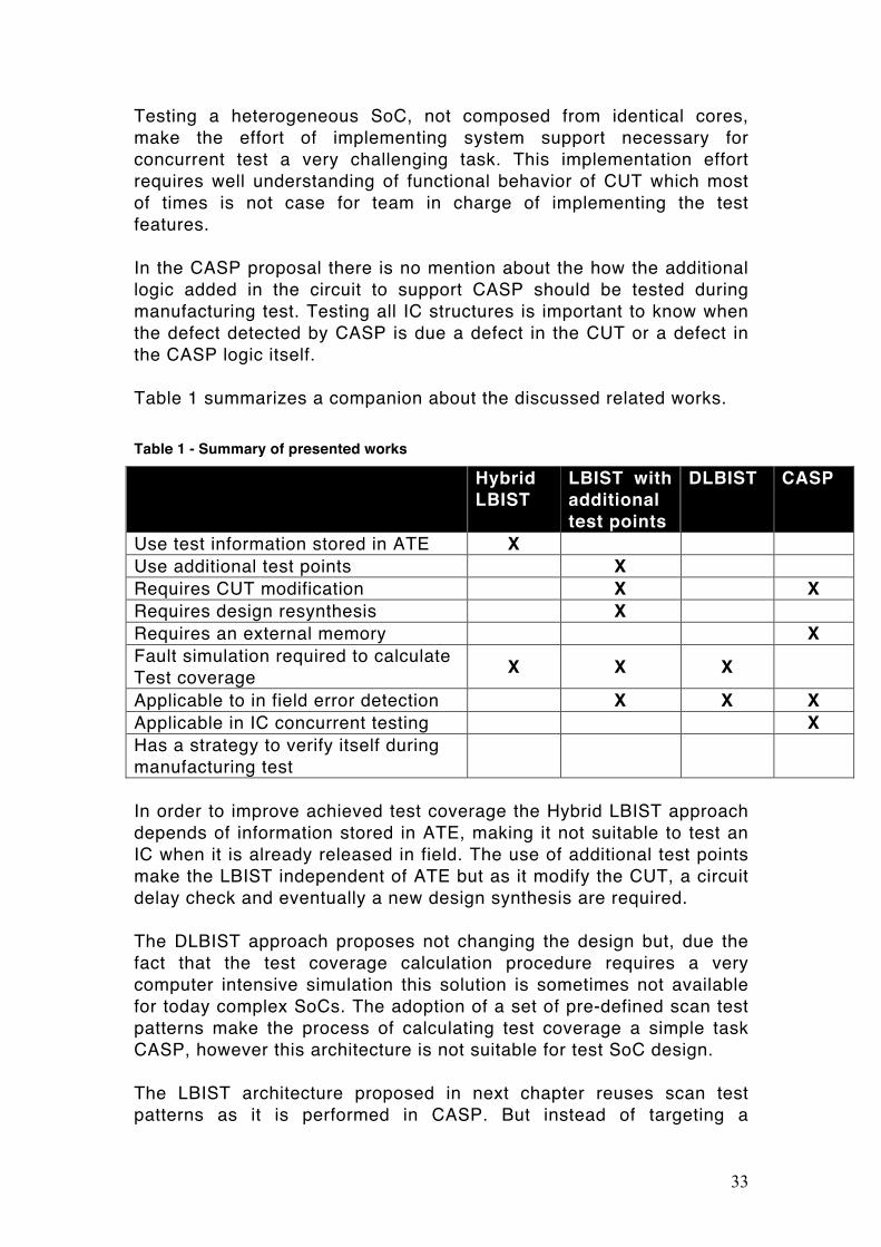
Testing a heterogeneous SoC, not composed from identical cores, make the effort of implementing system support necessary for concurrent test a very challenging task. This implementation effort requires well understanding of functional behavior of CUT which most of times is not case for team in charge of implementing the test features. In the CASP proposal there is no mention about the how the additional logic added in the circuit to support CASP should be tested during manufacturing test. Testing all IC structures is important to know when the defect detected by CASP is due a defect in the CUT or a defect in the CASP logic itself. Table 1 summarizes a companion about the discussed related works. Table 1 - Summary of presented works
Hybrid LBIST
LBIST with additional test points
DLBIST CASP
Use test information stored in ATE X Use additional test points X Requires CUT modification X X Requires design resynthesis X Requires an external memory X Fault simulation required to calculate Test coverage X X X
Applicable to in field error detection X X X Applicable in IC concurrent testing X Has a strategy to verify itself during manufacturing test
In order to improve achieved test coverage the Hybrid LBIST approach depends of information stored in ATE, making it not suitable to test an IC when it is already released in field. The use of additional test points make the LBIST independent of ATE but as it modify the CUT, a circuit delay check and eventually a new design synthesis are required. The DLBIST approach proposes not changing the design but, due the fact that the test coverage calculation procedure requires a very computer intensive simulation this solution is sometimes not available for today complex SoCs. The adoption of a set of pre-defined scan test patterns make the process of calculating test coverage a simple task CASP, however this architecture is not suitable for test SoC design. The LBIST architecture proposed in next chapter reuses scan test patterns as it is performed in CASP. But instead of targeting a

34
concurrent testing in small localized parts of the design, the work proposes testing the whole system in a non concurrent way. In other words, while the system is tested no functional activity is allowed in the circuit. This decision makes the proposed solution suitable to be used in SoCs that are not composed off identical cores. Also, due the fact that the proposed solution reuses test patterns from ATPG no fault simulation procedure is required. An aspect that was neglected by all presented works is how to check correctness LBIST structure before its application to self-testing of circuits. The next chapter proposes the compressed scan test patterns based LBIST architecture that store test data information in an external memory and can be used to verify a SoC when it is already in field. The proposed development flow address also the aspect of assuring correctness LBIST module before using it to self-test circuits in field.

35
Chapter 4 - General strategy for implementing a scan test pattern based LBIST.
Architecture proposal The scan test pattern LBIST can be used for system failure diagnosis when the IC is already released on field. Figure 14 presents the proposed LBIST architecture, which uses compressed patterns stored inside an internal memory to feed internal scan chains instead of using PRPG as in traditional LBIST approach. The scan compressor, don’t care (X) masking and decompressor modules can be implemented by EDA tools, for example Synopsys DFT Compiler. The LBIST controller, the internal memory, the input register and the MISR registers have to be implemented manually. Output response compaction is performed by a 128 bits MISR. Good and bad circuits produce different signatures. The probability that the signature of a bad circuit will be the same as signature of a good circuit is very small. This problem is known as aliasing. According to [9] the aliasing probability of a MISR asymptotically converges to 2-m for a m bit MISR. The 128 bits MISR has a very low aliasing probability 2-128. Compressed scan input patterns and one output response signature are stored in an external memory shared with program memory. This approach enable the updating of used test data in the same way the program memory is updated on field according to product evolution. During system boot up the test data is downloaded from external memory to an internal chip memory. This flow is managed by an existing internal functional block, such as microcontroller core and on-chip test controller. The main requirements for the proposed LBIST architecture are:
• Availability of an external memory already connected to IC; • Presence in the CUT of one functional core, such as a
microcontroller. This functional core will be in charge of downloading scan test patterns from external memory and feeding the internal memory;
• Presence of the test-access-port (TAP) module. The TAP is used to configure LBIST test mode and also serve as interface to get test result.

36
Figure 14 - Compressed scan pattern LBIST architecture
The use of a dedicated memory instead of sharing space with an existing board memory is also possible. But, this configuration requires some modifications in the proposed architecture, such as using a dedicate module to download test patterns from this memory to chip. In fact, reusing an already connected external memory represents less changes overhead in customer solution because it avoid change in the board design and creates the possibility of using an existing functional block, such an microcontroller core inside the CUT to download test patterns during boot up. Any failure in the process of downloading the test patterns from external memory to internal memory will result in earlier failure detection by LBIST test controller. The scan test patterns download procedure is executed during system boot up. Figure 15 illustrates the proposed flow for using an autonomous LBIST. During boot up the compressed input patterns and one 128bit output signature is downloaded from board program memory to chip internal memory. After that, the LBIST test mode is configured using a Test-

37
access-port (TAP) [2]. The autonomous test is started, the test signature is generated and the result of test signature comparison is stored in test status registers. Test result registers are available through TAP.
Figure 15 - Autonomous LBIST execution flow
During autonomous LBIST test-mode, all scan chain clock domains are driven by only one external clock. TAP clock (TCK) is used as unique external test clock. Due the fact that the IC could be connected at board level with other peripherals an isolation during LBIST test-mode is implemented. In order to not disturb board peripherals all IC pins must tied to high Z during LBIST test mode execution.
! Improving test coverage with multiple boot ups.
The test coverage archived by LBIST test mode is conditioned by the number of test patterns that can be stored in internal memory. In order to surpass this limitation the solution of using a test flow with multiple boot ups is proposed.

38
High test coverage (more than 98%) for test system in field could be achieved while increasing the amount of test data stored outside chip memory. The major challenge continues to be how to download this data to feed the internal scan chains. Adding new board components is not a good solution because it requires changing the customer board. A better approach to improve system diagnosis fault coverage without the need of using a new external component is to repeat the flow of loading test data during boot performed by an existing functional block presented in section before. In this case different sets of input patterns and signature are loaded at each different boot up time from external memory.
Figure 16 - Improving LBIST test coverage with multiples boot ups
The multiple boot test procedure is illustrated in Figure 16. The multiple boot ups are performed sequentially without intervention. For the end-user the complete LBIST test flow with multiple boot ups is seen like a unique longer boot up. A critical point is this approach is the boot up impact in total test application time. The boot up process is not instantaneous because of some initialization procedures as PLL locking. In consequence the improvement of test coverage using multiple boot ups implicates in an increase in the test application time.
! Complementing test coverage in a laboratory environment.
An alternative to improve test coverage of the system is to use the proposed LBIST structure to enable feeding the CUT with test data from a host computer instead of using an external program memory. In

39
laboratory environment the test-application-time (TAT) and test-data-volume (TDV) are not critical. A host computer is used to connect to CUT through the test-access-port (TAP). This alternative enables complementing test coverage achieved by LBIST test mode which is limited by chip and board storage memory. The advantages of using TAP controller for this task are:
! TAP is already included in the design; ! TAP associated pins are not used by the application board,
making them free to use in laboratory environment. A software tool interface can aid the connection process between the host computer and an intermediary board programmed to control a TAP interface. Using the TAP interface the host computer will be able to apply a deterministic set of scan test patterns as well as to check the test results. This flow is illustrated in Figure 17.
Figure 17 - Host computer – JTAG/TAP control flow
The Proposed development flow The effort for downloading the scan test patterns from external memory to internal memory is part of functional design of CUT, therefore out of scope of this proposal. This session concentrates the explanation the integration of LBIST modules in the current flow. Inside Digital IC development flow, see Figure 18, the effort for implementing the proposed scan test patterns based LBIST is concentrated in DFT Insertion and ATPG phases.

40
Figure 18 - Scan test pattern LBIST in Digital IC development flow
The proposed LBIST development flow starts after the CUT scan chains insertion task, see Figure 19. The number and length of implemented scan chains are used to develop internal test memory and LBIST core modules. The LBIST modules are: LBIST controller, MISR, Input Registers. LBIST core is developed to drive all functional clock domains with a unique source, the TAP clock. LBIST core is verified, synthesized as netlist. Then LBIST core netlist pass through a scan chain insertion as isolated module from the rest of system. The result is a LBIST core scan ready netlist and a LBIST individual test protocol.

41
Figure 19 - Scan test patterns based LBIST development flow
After that, the TAP is modified to implement LBIST testmode. Basically new test configuration registers and test status registers are added in the existing TAP netlist. Registers for controlling individually each functional clock are also implemented in the TAP. A new chip top level system is created with original CUT scan ready netlist, modified TAP netlist, LBIST scan ready netlist and some muxes to make the integration between parts. At this point two test protocols are created. The first will be used during ATPG for manufacturing test, where the whole system including LBIST core is checked against fabrication defects. The second will be used to generate scan test pattern for scan test pattern LBIST test mode. The ATPG flow is modified to generate patterns for the two different test protocols. When generating the test pattern for manufacturing the LBIST core is loaded in the flow as a hard-macro with already specific scan chains and specific test protocol. The isolation between LBIST core and original CUT can be see in Figure 20. In order to test the LBIST circuit new pins are added at the top level chip.

42
Figure 20 - Isolation between LBIST scan chains and CUT scan chains
As result, this configuration enables testing the proposed LBIST structure to be tested during manufacturing test. This feature is important to assure the correctness of LBIST module before using it in the field self-test process. When generating test patterns for LBIST testmode, the LBIST core is treated as a black box. This informs the tool that no test pattern should be generated to test LBIST core. All pattern generated will exercise only the original CUT part of circuit, as shown in Figure 21.
Figure 21 - Test protocol configuration for generating pattern for LBIST

43
At end of ATPG flow two patterns sets are available. The patterns used for implementing the LBIST test mode can now be stored in the external memory. The proposed flow does not defines how exactly the pattern stored in external memory should be downloaded into the chip. We understand that this definition is part of functional specification of system. Independent of way that test data information is downloaded inside chip the LBIST controller supposes that the information is already available when the LBIST test mode starts.

44
Chapter 5 - Case study This chapter applies the proposed strategy in a real world design to discuss the implementation challenges of the scan test pattern based LBIST.
Test case overview In order to illustrate the application of proposed LBIST, a 3G Wireless SoC already in production on ST Microelectronics 90nm process has been used. A testcase architecture overview is shown in Figure 22.
• It is a WCDMA baseband divided in two parts: The access part and the application part. With total of 250406 flip-flops.
• The circuit is running at 208 MHz on it fastest part. • It is based on a DSP and two microcontrollers. • It contains 4*PLLs, 2 * 6.5 bits sigma delta differential dual
channel AD converter, a 10 bits dual channel DA converter and a 10 bits general purpose AD converter.
• Manufacturing test uses eleven clock domains for testing. • Another important point in this 3G Baseband SoC is the presence
of test application port (TAP) used for test mode selection and to access test control and status registers.
Figure 22 - Testcase overview

45
This testcase adopts a wide variety of fault models aiming for maximizing the silicon quality. This fact pushes the overall scan vector count up with a significant increase in the cost of test. To minimize this criticality the use of advanced techniques for pattern compaction has become a key-aspect in the global testability strategy. The solution available and supported at ST Microelectronics is the Synopsys Adaptive Scan a broadcast compression solution. Figure 23 shows the comparison of overall reduction between test in compressed mode and non compressed mode for Stuck-at faults (SAF) patterns.
Figure 23- Test data volume for compressed and non-compressed test modes
Depending of number of applied patterns the TAT and TDV reduction for manufacturing test vary from 40 to 60 times, Figure 24 shows the coverage according with number of patterns. It shows that the better reductions are achieved with low pattern count and also close the final test coverage. This work uses compressed scan test patterns for only SAF without fast-sequential ATPG run. In this case the achieved test coverage for the original testcase design was 98.42%. More details about ATPG are available in Appendix A.
Figure 24 - Test data volume reduction for different test coverage
LBIST test memories The 3G Wireless Baseband SoC used as testcase was validated to work with external program memories of 128, 256, 512, 1024, 2048 Mb.

46
Only one output test signature is used for each 91 input patterns. The input patterns in Scan_compress mode have 5330 bits (65 external chains * 82 longest scan chain) plus 264 bits required to reconstruct test scenario. It was decided to replicate an existing system memory of 512 Kb to use in the proposed LBIST architecture. Considering an internal memory of 512 Kb it represents only 0.4% of a 128 Mb program memory. Adding a 512 Kb internal memory for LBIST test mode has an impact in IC area. The overhead of adding this new memory represents an increment of 4% in total IC memory area. For single boot and multiple boot up modes Table 2 presents the used space on program memory that represents storing a given number of patterns plus one 128-bit signature for each 91 patterns. Table 2 - Occupied space on program memory
#Patterns Test coverage
Input patterns
Signature 128 Mb 256 Mb 512 Mb 1024 Mb
2048 Mb
64 65,15% 358016b 128b 0,28% 0,14% 0,07% 0,03% 0,02% 91 - 509024b 128b 0,40% 0,20% 0,10% 0,05% 0,02% 6956 98,41% 38911864b 13952b 30,41% 15,21% 7,60% 3,80% 1,90% 14166 98,84% 79244604b 28416b 61,93% 30,97% 15,48% 7,74% 3,87% The registered test coverage was based on experimental data for testcase IC using Synopsys TetraMAX v2007.12-sp4 without insertion of extra test points. Highlighted cells represents situation when the occupied memory percentage is lower than 10%. The test application time for applying each pattern set without boot up time is presented in Table 3. Table 3 - Test application time
#Patterns #Boot ups Test application time (in seconds) 64 1 0,0001079 91 1 0,0001527 6956 73 0,0117579 14166 148 0,0238212 The TAP clock frequency and synthesized scan chains frequency determines the test clock frequency for LBIST test mode. The clock frequency of presented testcase was 50 MHz.

47
Developed LBIST core The modules in charge of implementing the proposed LBIST feature were inserted at top level of 3G Wireless Baseband SoC design. It was implemented two main test functionalities:
a. Autonomous LBIST: System is tested autonomously. This test mode assumes that a subset of test patterns was already downloaded into an internal memory during system boot up.
o Event Flow: 1. The TAP controller receives and executes a test
mode configuration bit stream. 2. MISR is reset to a known state. 3. LBIST test controller changes CUT to shift mode
state. Scan chains are filled with values stored in internal memory. The values are shifted once all scan chain inputs are filled. All CUT outputs are stored in MISR.
4. All scan chains contents are filled for one pattern. 5. LBIST test controller change to capture state. Result
was captured. 6. A loop for step 4 is done until all input patterns are
ready from internal memory. 7. MISR will have the final test signature. 8. The result of checking MISR signature against
stored reference signature is stored in a test result bit register. Test process is finished.
b. Laboratory mode: System is tested iteratively. Input patterns are
passed through TAP and test procedure and output response checking are controlled by an external Host computer.
1. The TAP controller receives and executes a test mode configuration bit stream.
2. MISR is reset to a know state. 3. LBIST test controller change CUT to shift mode
state. Input registers are filed with data from TAP. Scan chains are filled with values stored in Input registers. The values are shifted once all scan chain inputs are filled. All CUT output is stored in Output registers and shift out through TAP.
4. LBIST test controller change to capture state. Result captured.
5. A loop for step 3 is done until the system is initialized again.
The top architecture of LBIST controller is presented in Figure 25. The LBIST controller module was the more challenging and time consuming during prototyping phase. It was constructed in to support the

48
functionality, as autonomous LBIST and as laboratory test, as fully independent from each other.
Figure 25 - LBIST controller internal architecture
The LBIST_MEM sub-module is responsible for implementing the scan test pattern based LBIST test mode. It reads the patterns from an internal memory to feed the CUT through the scan input ports and emulates the same shift and capture mode behaviors as if performed by an ATE during production testing. The output results feed a 128-bit MISR register, which compute final the test signature. After all patterns are read a comparison is performed between the test signature from MISR and a reference signature read from the memory. The test results are stored in the test status register (TSR) accessible through the TAP. In charge of implementing laboratory test capabilities is the LBIST_LAB module. Its consists of a test mode controller, input registers used to bridge test stimuli from TAP input to the CUT scan input ports and a output registers to output test results. The PULSER module is responsible for generating test shift and capture clocks pulses for the eleven clock domains of CUT. As in manufacturing test process each clock domain can be activated or deactivated depending on the test mode configuration. LBIST_OUTPUT_MUX includes a set of muxes, which are in charge of switching LBIST controller module outputs between the two internal test

49
mode controllers’ outputs. LBIST_PULSER_MUX encompasses a set of muxes in charge of switching control inputs of internal PULSER module
TAP Modifications During autonomous LBIST test-mode, the eleven test clocks domains of testcase SoC are driven by only one external clock. TAP clock (TCK) is used as unique external system clock. It is important to say that new generations of WCDMA Baseband IC have already an integrated on-chip-clock (OCC) that could be used to enable the testing of delay faults. Another important point to not disturb output peripherals on the board during LBIST test-mode execution is to tie all pins to high Z. In order to maintain the same control capability from tester machine of controlling each clock domain separately, it was decided to implement additional bits in the test controller register to control the eleven system clock-domains individually. Together with specific test pattern configuration this data is used to control an internal module during clock gating procedure for shift and capture modes. More details about the new test mode control registers and test status registers implemented in the TAP see Appendix B.
Integration of LBIST core in the system One of the challenges resolved during implementation was how to make it possible to reuse of the same scan test patterns used during manufacturing test. In this case we need to reproduce the same test procedure performed by ATE, taking care during capture mode do not lose any controllability while driving specific values of internal signals and also to avoid any lack of observability while measuring signal values. The LBIST module is should be connected Scan in/Scan out signals and other ports of CUT used to create the test scenario. In order to connect the LBIST module with CUT a 528 input | 264 output MUX is necessary. In others words 264 binary MUX cells are used. A clear drawback in this implementation decision is that it can impact in an additional place and route effort to connect all signals between LBIST module and the CUT. The final implemented architecture (see Figure 26)!utilizes only the 5 pins of TAP. LBIST controller takes controls of the system one time the LBIST test mode is configured. In autonomous LBIST test mode the LBIST controller starts reading the test patterns from internal memory. At end the MISR generates one signature. The signature is compared with a reference and the answer is stored in test status register.

50
The LBIST controller, MISR and system muxes area represents less than 0.01% of complete design synthesized area.
Figure 26 - Implemented architecture
ATPG for Manufacturing and for LBIST mode In last chapter it was proposed a flow to generate two different test protocols targeted to enabling manufacturing test and LBIST patterns generation. Besides the test protocol were generated the ATPG was not supported in DFT MAX 2007.12 tool version. Some cooperation with Synopsys support team will be necessary to make proposed ATPG flow available at Synopsys tools. Therefore it was decided to verify the rest of flow with pattern generated from to test only CUT. For this, the test protocol that recognizes only the CUT and not the LBIST core was used.
Results Table 4 - Result summary
CASP Scan test pattern based

51
(OpenSPARC T1 multicore)
LBIST (3G Wireless Baseband SoC)
Number of Flip-flops 20234 (per processor core)
250406
Size of internal memory 6144 bits 512.000 bits
Test compression implemented 10x (From EDA tools)
40x – 60x (From EDA tools) plus MISR output compression implemented by LBIST architecture.
Number of test patterns contained in the internal memory
1 91
Stuck-at patterns 609 (99,49%) 14166 (98,84%) Test data volume ~5,3 Mb ~80 Mb Test frequency 150 MHz 50MHz
Modification in CUT Processor cores modified to support CASP.
Muxes added to support test data from LBIST module.
Test pattern download mechanism Implemented by CASP Part of functional design. Not
implemented by LBIST core.
Total test time
~1 sec data transfer time plus ~0.2 sec test application time. (for one processor) core)
~0,02 sec test application time plus time of 148 system boot ups.
IC Area overhead <0.01% of digital circuit area
<0.01% of digital circuit area. Plus 4% of overhead in internal memory area.
Table 4 present a result summary of the proposed LBIST architecture and compare it with results of CASP [6] solution. The proposed scan test patterns based LBIST architecture was implemented in a 3G Wireless SoC. In contrast of the multicore architecture used by CASP our testcase does not support testing isolated parts of the design. The entire system should be tested at same time. Due the fact that the LBIST testcase has far more flip-flops and also the decision of storing 91 patterns for each boot up, makes the LBIST internal memory bigger when compared with CASP internal buffer.

52
The use of a MISR to compact output signature acts in the reduction of total test data and contributes in making it possible storing more test data in internal IC memory. The total test application of the proposed LBIST is approximately 0,02 seconds test application time plus the time required for performing 148 system boot ups. The IC area overhead of the proposed LBIST solution is less than 0.01% of total design synthesized area and the 512 Kb internal memory represent an overhead of 4% of IC memory area. The developed testcase uses 7,60% of a 512 Mb external memory to achieve 98,41% of test coverage.

53
Chapter 6 - Conclusions This work proposes a strategy for reuse manufacturing test patterns to create a LBIST test mechanism. The proposed LBIST mechanism has the target uncover defects that could occur due to the wear out of the circuit when it is already released in field. The proposed LBIST architecture stores test data information in an external memory and utilize a functional block to download it into chip and verify the SoC. A scan test pattern based LBIST flow that integrates to current Digital IC Development flow is proposed. Based on already implemented scan chain features a LBIST core module is developed and integrated at chip top level. The proposed flow requirements are:
• Availability of an external memory already connected to IC; • Presence in the CUT of one functional core, such as a
microcontroller. This functional core will be in charge of downloading scan test patterns from external memory and feeding the internal memory;
• Presence of the test-access-port (TAP) module. The TAP is used to configure LBIST test mode and also serve as interface to get test result.
The LBIST architecture implementation in a real world SoC was presented. The IC area overhead of proposed LBIST solution is less than 0.01% of total design synthesized area and the 512 Kb internal memory represent an overhead of 4% of IC memory area. The developed testcase uses 7,60% of a 512 Mb external memory to achieve 98,41% of test coverage. The total test application time to achieve this coverage is approximately 0,02 seconds test application time plus the time required for performing 73 system boot ups. One of challenges during test case implementation was how to make the system reuse the same scan test patterns used during manufacturing test. Specifically how to reproduce the same test procedure performed by ATE, taking care during capture mode to not lose any controllability while driving specific values of internal signals and also to avoid any lack of observability while measuring signal values. This challenge was overcome taking care in the understanding of test flow for implementing the same behavior in the proposed LBIST core. Another challenging point was the definition of how the LBIST core integrated in the system should be tested during manufacturing test. The LBIST core internal scan chains must not interfere in the test of

54
rest of design. A new flow to generate two set of different scan test pattern was proposed. But due some DFT tool limitation it was not possible to implement the complete flow, To overcome this problem the test patterns generated for the systems without LBIST core were used to validate the rest of flow. The proposed work makes an initial proposal of an architecture and flow to implement a LBIST mechanism that utilizes scan test pattern to test a SoC already released in field. Future research possibilities include:
• Efficient process of downloading the test data information from
an external memory to reduce the boot up time. • Analyze the vulnerability of proposed LBIST architecture to side
channels attacks [10].

55
Bibliography [1] Bardell, P.H., W.H. McAnney, and J. Savir, ”Built-In Test for VLSI:
Pseudorandom Techniques,” John Wiley and Sons, New York, 1987. [2] IEEE Standard 1149.1 Test Access Port and boundary-scan architecture,
2001. [3] D. Das and N.A. Touba. Reducing test data volume using external/lbist
hybrid test patterns. In Test Conference, 2000. Proceedings. International, pages 115–122, 2000.
[4] A. Jas, J. Ghosh-Dastidar, Mom-Eng Ng, and N.A. Touba. An efficient test
vector compression scheme using selective huffman coding. Computer-Aided Design of Integrated Circuits and Systems, IEEE Transactions on,22(6):797–806, 2003.
[5] R. Kapur, S. Mitra, and T.W. Williams. Historical perspective on scan
compression. Design & Test of Computers, IEEE, 25(2):114–120, 2008. [6] Yanjing Li, Samy Makar, and Subhasish Mitra. Casp: Concurrent
autonomous chip self-test using stored test patterns. In Design, Automation and Test in Europe, 2008. DATE ’08, pages 885–890, 2008.
[7] E.J. Marinissen, B. Vermeulen, R. Madge, M. Kessler, and M. Muller.
Creating value through test. In Design, Automation and Test in Europe Conference and Exhibition, 2003, pages 402–407, 2003.
[8] N.A. Touba. Survey of test vector compression techniques. Design & Test
of Computers, IEEE, 23(4):294–303, 2006. [9] T.W. Williams and W. Daehn. Aliasing errors in multiple input signature
analysis registers. In European Test Conference, 1989., Proceedings of the 1st, pages 338–345, 1989.
[10] Bo Yang, Kaijie Wu, and Ramesh Karri. Scan based side channel attack on
dedicated hardware implementations of data encryption standard. In Test Conference, 2004. Proceedings. ITC 2004. International, pages 339–344, 2004.
[11] C. Barnhart et al., “OPMISR: the foundation for compressed ATPG
vectors,” in , 2001, 748-757, doi:10.1109/TEST.2001.966696. [12] Jinkyu Lee e N.A. Touba, “Combining linear and nonlinear test vector
compression using correlation-based rectangular encoding,” in , 2006, 6 pp., doi:10.1109/VTS.2006.25.
[13] TetraMAX ATPG User Guide, Version A-2007.12-SP4, June 2008,
Synopsys.
[14] DFT MAX User Guide: Adaptive Scan, Version A-2007.12, July 2008, Synopsys.

56
[15] M.J. Geuzebroek, J.T. van der Linden, e A.J. van de Goor, “Test point insertion for compact test sets,” in , 2000, 292-301, doi:10.1109/TEST.2000.894217.
[16] M.J. Geuzebroek, J.T. van der Linden, e A.J. van de Goor, “Test point
insertion that facilitates ATPG in reducing test time and data volume,” in , 2002, 138-147, doi:10.1109/TEST.2002.1041754.
[17] Gert Jervan et al., “Hybrid BIST Optimization Using Reseeding and Test
Set Compaction,” in , 2007, 596-603.
[18] M. Agarwal et al., “Circuit Failure Prediction and Its Application to Transistor Aging,” in , 2007, 277-286, doi:10.1109/VTS.2007.22.
[19] A. Jas et al., “An efficient test vector compression scheme using selective
Huffman coding,” Computer-Aided Design of Integrated Circuits and Systems, IEEE Transactions on 22, no. 6 (2003): 797-806, doi:10.1109/TCAD.2003.811452.
[20] Xiaoyun Sun, L. Kinney, e B. Vinnakota, “Combining dictionary coding and
LFSR reseeding for test data compression,” in , 2004, 944-947.
[21] C.V. Krishna e N.A. Touba, “Reducing test data volume using LFSR reseeding with seed compression,” in , 2002, 321-330, doi:10.1109/TEST.2002.1041775.
[22] Chih-Tsun Huang et al., “A programmable BIST core for embedded DRAM,”
Design & Test of Computers, IEEE 16, no. 1 (1999): 59-70, doi:10.1109/54.748806.
[23] S. Kim, M. Soma, e D. Risbud, “An effective defect-oriented BIST
architecture for high-speed phase-locked loops,” in VLSI Test Symposium, 2000. Proceedings. 18th IEEE, 2000, 231-236, doi:10.1109/VTEST.2000.843850.
[24] Test Pattern Validation User Guide, Version B-2008.09-SP2, December
2008, Synopsys.
[25] Seung-Moon Yoo, Seong-Ook Jung, e Sung-Mo Steve Kang, “2-level LFSR scheme with asynchronous test pattern transfer for low cost and high efficiency build-in-self-test,” in Proceedings of the 11th Great Lakes symposium on VLSI (West Lafayette, Indiana, United States: ACM, 2001), 93-96, doi:10.1145/368122.368874.
[26] G. Hetherington et al., “Logic BIST for large industrial designs: real issues
and case studies,” in Test Conference, 1999. Proceedings. International, 1999, 358-367, doi:10.1109/TEST.1999.805650.
[27] Harald Vranken, Ferry Syafei Sapei, e Hans-Joachim Wunderlich, “Impact
of Test Point Insertion on Silicon Area and Timing during Layout,” in Proceedings of the conference on Design, automation and test in Europe - Volume 2 (IEEE Computer Society, 2004), 20810, http://portal.acm.org/citation.cfm?id=969201.

57
[28] Gundolf Kiefer and Harald Vranken, “Application of Deterministic Logic BIST on Industrial Circuits,” In Proceedings IEEE International Test Conference (ITC (2000): 105--114, doi:10.1.1.7.3823.

58
Appendix A - Generating most efficient test patterns The compression scan feature brought by Synopsys tool made possible test data volume and test application time reduction up to 100x times. This fact make us think if is possible to use pattern ATPG created patterns instead PRPG patterns in the LBIST. In order to investigate the possibility of generating optimized test patterns, less test pattern possible for a given fault coverage, a series of ATPG experiments were performed. The first step was taking an ATPG reference flow for used SoC testcase from an existing report. This appendix describes flow decisions for generating patterns for the 3G Wireless Baseband SoC testcase. The appendix present results for pattern generation obtained in SAF compressed test mode. The tool version used for this runs was TetraMAX Z-2007.03.SP5. All tests were made on production based chips so with process considered TYPICAL. In order of using a specific version of TetraMAX that supports adding extra logic for avoiding unknown’s logic “X” propagation in the circuit, it was decided to rerun the same script on the new version, 2007.12. The first experiment was to modify the design and scripts to suppress unknown logic sources during ATPG. It is well known that unknown logic “X” sources in the design can mask some circuit data paths and lower the overall test coverage and also sometimes increase the number of patterns needed to archive the same coverage in the design without “Xs” sources. There were some static “X” sources that are known in design. There are basically ROMs and Fuses. I have modified the ROM and Fuses description to ensure that they will not propagate Xs. I have also black boxed the fuses and ADC/DAC modules to force a “X” sources reduction in the design. There is also a dynamic X source in the design that was found only during pattern simulation. It was a specific path marked with a TIE X command in the original script. For unknown logic “X” free ATPG I have only removed this line of the script. The results of these experiments were an improvement of 0.2 % in system final fault coverage. After that, a series of ATPG runs with objective to study the impact of some tool parameters in test coverage was performed. During theses experiments also information regarding Memory usage and tool runtime were collected. A summary of experiments is shown in Table 5. Even with design and scripts modification it was not possible to suppress all unknown logic sources “X” in the design. The numbers of violations caused by presence of “X” were reduced from 1039 occurrences to

59
249. Despite the good results provided by experiment 5, those result were not taken in account in the final results because the insertion of additional test points is not compatible with current company test insertion flow. Some points to highlight are:
• Reference design achieved test coverage of 97,49% with 14858 patterns.
• One of runs experiment 6 that combines -abort_limit 10000 and -basic_detects_per_pattern 20 achieved the best result among all experiments with test coverage of 97,53% with 6552 patterns. It corresponds a data reduction of 55,90%.
• Taking in account only the first 64 patterns, it was achieved an upgraded in test coverage from 63,61% to 65,94%.
• The best final coverage achieved by all experiments was 98,05% with 14315 patterns.
Table 5 - ATPG experiments summary
Experiment Description Number of different ATPG runs
1 Simulate a design without unknown logic “X” sources 2
2 Investigate the impact of entropy on pattern count and test coverage with atpg fill_adjacent parameter
7
3 Investigate the impact of higher values for abort limit parameter 3
4 Investigate the impact of basic_detects_per_pattern parameter in the creation of most efficient pattern at beginning of ATPG
8
5 Investigate the insertion of additional test points to reduce pattern count 9
6 Investigate the combination of parameters of previous experiments 5
Total 34 One of main constraints of proposed architecture is to use as less memory as possible to implement the test procedure. After running those experiments the main conclusion was that ATPG flow can be managed to provide an improvement in the generation of more efficient patterns. But, this improvement is very small when compared against Adaptive Scan compression scheme implemented during insertion of test scan chains by Synopsys tools. In fact Adaptive Scan is giving the

60
biggest "bang for the buck“ on compression and not the developed optimized ATPG flow. In order to achieve the minimum test coverage of 65% for our testcase it is needed at least an internal memory of 512 kb. This represents an overhead of 4% in internal memory IC area. For the external memory this represents an overhead of 0.4% that is an acceptable trade-of for this feature.

61
Appendix B - TAP Modifications This appendix describes the proposed modifications on test control register and test status register (TCR+TSR) modules is order to enable integrations with LBIST module. TCR and TSR are concatenated in a unique shift register that can read and write at same time. They represent a unique 525 bits long register accessible using TAP instruction “10000” while putting new control bits in TDI port and reading status bits in TDO port.
TDI" TCR TSR TDO" It is not necessary shift all 525 positions to setup test mode or to get test status bits because TCR part is closer to TDI and TSR is closer to TDO. In order to set control bits it is needed to shift in only the size of TCR and to get test status it is needed to shift out only the size of TSR. The test setup bit feeding is performed starting with last programmed bit tst_acc_reset_control and finalized with tst_scanmode. After that an UPDATE INSTRUCTION REGISTER is executed, followed with two clock cycles in order to update the contents of TMC. Based on this fact, the LBIST control and status bits will be located between TCR and TSR registers, as in the figure below. The new test setup starts with feeding LBIST control bits and finish with a specific TAP instruction to update registers plus two TCK pulses. This configuration does not change the test mode configuration and status read sequences of already implemented test modes.
TDI" TCR LBIST CTR
LBIST STATUS TSR TDO"
In total of 148 bits are added in TCR+TSR, the table describes the use and position for each of them. Table 6 - Proposed modification in TCR+TSR
Bit
num
Signal name Signal type Description
157 tst_acc_reset_control constrained_dynamic Separate Access reset control
158 tst_lbist_start static Start the Lbist test modes.
Drives LBIST TDO MUX and SOCLBIST_top internal states.
159 tst_lbist_mode static When enabled use already internal stored patterns to

62
perform an autonomous LBIST.
When disabled use TDI to fill internal scan chains and TDO to scan outputs.
Drives SOCLBIST_top internal mux called patterns_mux. When
Drives LBIST TDO MUX. When enabled output data for LBIST test controller. When disabled represents unmodified path.
160 tst_lbist_enablePO_ETM_TRACE_SYNC static Enable pulses for PO_ETM_TRACE_SYNC during LBIST.
161 tst_lbist_enablePO_ETM_TRACE_PKT7 static Enable pulses for PO_ETM_TRACE_PKT7 during LBIST.
162 tst_lbist_enablePO_ETM_TRACE_PKT6 static Enable pulses for PO_ETM_TRACE_PKT6 during LBIST.
163 tst_lbist_enablePO_ETM_TRACE_PKT5 static Enable pulses for PO_ETM_TRACE_PKT5 during LBIST.
164 tst_lbist_enablePO_ETM_PIPE_STAT2 static Enable pulses for PO_ETM_PIPE_STAT2 during LBIST.
165 tst_lbist_enablePO_ETM_PIPE_STAT1 static Enable pulses for PO_ETM_PIPE_STAT1 during LBIST.
166 tst_lbist_enablePO_ETM_PIPE_STAT0 static Enable pulses for PO_ETM_PIPE_STAT0 during LBIST.
167 tst_lbist_enablePO_EMIF_1_CLK static Enable pulses for PO_EMIF_1_CLK during LBIST.
168 tst_lbist_enablePI_TAP_CLK static Enable pulses for PI_TAP_CLK during LBIST.
169 tst_lbist_enablePI_POW_RST_N static Enable pulses for PI_POW_RST_N during LBIST.
170 tst_lbist_enablePI_EMIF_1_RET_CLK static Enable pulses for PI_EMIF_1_RET_CLK during LBIST.
171 tst_lbist_enablePIO_MMC_CLK static Enable pulses for PIO_MMC_CLK during LBIST.
172 tst_lbist_enablePIO_EMIF_0_SD_CLK static Enable pulses for PIO_EMIF_0_SD_CLK during LBIST.
173-
301
tst_lbist_signature [127:0] non_scan_observe LBIST test signature.
302 tst_lbist_result non_scan_observe Enabled when LBIST test is performed with success.
303 tst_lbist_patternsDownloaded
non_scan_observe Enabled when patterns download from ARM functional block is accomplished with success.
304 tst_app_pll13xlockx non_scan_observe Application PLL 13M lock signal.
Another point is that as TCR registers are part o scan chains, shadow register are used to preserve TCR output values during SCAN

63
testmode, as shown in Figure 27. When tst_scanmode TCR bit is high, no TCR output can be updated anymore but the TCR can still be programmed
Figure 27 - TCR static bit description
The connections between TCR outputs and control muxes used during LBIST testmode are showed in Figure 28.
Figure 28 - TCR connections with LBIST muxes
The connections between TSR in LBIST module in charge of pulsing clocks during shift and capture mode are show in Figure 29.

64
Figure 29 - Connections between TCR and module in charge of pulsing clock
Basing on TCR static bit description of Figure 27 the TSR static bit description has a similar structure to deal with shift logic but without shadow part. Another difference is the existence of an additional mux controlled by LBIST test controller that has as input the previous register value and the value coming from LBIST test controller as show in Figure 30.
Figure 30 - TSR description