A graphene Zener–Klein transistor cooled by a hyperbolic...
21
ARTICLES https://doi.org/10.1038/s41565-017-0007-9 A graphene Zener–Klein transistor cooled by a hyperbolic substrate Wei Yang 1 , Simon Berthou 1 , Xiaobo Lu 2 , Quentin Wilmart 1 , Anne Denis 1 , Michael Rosticher 1 , Takashi Taniguchi 3 , Kenji Watanabe 3 , Gwendal Fève 1 , Jean-Marc Berroir 1 , Guangyu Zhang 2 , Christophe Voisin 1 , Emmanuel Baudin 1 and Bernard Plaçais 1 * 1 Laboratoire Pierre Aigrain, Département de physique de l’ENS, Ecole normale supérieure, PSL Research University, Université Paris Diderot, Sorbonne Paris Cité, Sorbonne Universités, UPMC Univ. Paris 06, CNRS, 75005 Paris, France. 2 Beijing National Laboratory for Condensed Matter Physics and Institute of Physics, Chinese Academy of Sciences, Beijing 100190, China. 3 Advanced Materials Laboratory, National Institute for Materials Science, Tsukuba, Japan. *e-mail: [email protected] © 2017 Macmillan Publishers Limited, part of Springer Nature. All rights reserved. SUPPLEMENTARY INFORMATION In the format provided by the authors and unedited. NATURE NANOTECHNOLOGY | www.nature.com/naturenanotechnology
Transcript of A graphene Zener–Klein transistor cooled by a hyperbolic...
Articleshttps://doi.org/10.1038/s41565-017-0007-9
A graphene Zener–Klein transistor cooled by a hyperbolic substrateWei Yang1, Simon Berthou1, Xiaobo Lu2, Quentin Wilmart1, Anne Denis1, Michael Rosticher1, Takashi Taniguchi3, Kenji Watanabe 3, Gwendal Fève1, Jean-Marc Berroir1, Guangyu Zhang2, Christophe Voisin1, Emmanuel Baudin 1 and Bernard Plaçais 1*
1Laboratoire Pierre Aigrain, Département de physique de l’ENS, Ecole normale supérieure, PSL Research University, Université Paris Diderot, Sorbonne Paris Cité, Sorbonne Universités, UPMC Univ. Paris 06, CNRS, 75005 Paris, France. 2Beijing National Laboratory for Condensed Matter Physics and Institute of Physics, Chinese Academy of Sciences, Beijing 100190, China. 3Advanced Materials Laboratory, National Institute for Materials Science, Tsukuba, Japan. *e-mail: [email protected]
© 2017 Macmillan Publishers Limited, part of Springer Nature. All rights reserved.
SUPPLEMENTARY INFORMATION
In the format provided by the authors and unedited.
NATuRE NANoTEChNoLoGY | www.nature.com/naturenanotechnology

A graphene Zener-Klein transistor cooled by a hyperbolic
substrate. (supplementary)
Wei Yang, Simon Berthou, Xiaobo Lu, Quentin Wilmart, Anne Denis, Michael
Rosticher, Takashi Taniguchi, Kenji Watanabe, Gwendal Feve, Jean-Marc Berroir,
Guangyu Zhang, Christophe Voisin, Emmanuel Baudin, and Bernard Placais
1

Cu
rre
nt
no
ise
(p
A2/H
z)
0
50
100
150
Frequency (GHz)
0 2 4 6 8 10
0.5V
1.5V
2.5V
3.5V
a b
FIG. S-1: Panel a) : scheme of the measuring set-up. Panel b) : typical current noise spectrum
measured in the 0–10 GHz band width.
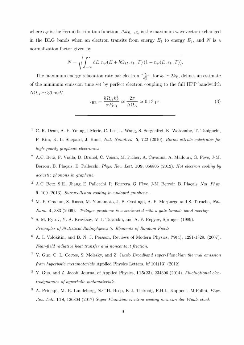
I. EXPERIMENTAL SETUP AND NOISE CALIBRATION
A schematic of our noise thermometry setup is illustrated in Figure S-1-a. The principle
is derived from the 0–1 GHz setup of Ref.2 which has been upgraded to the 0–10 GHz
bandwidth to overcome the 1/f -noise at the ultimate currents of our experiment. The
graphene sample, embedded in a coplanar wave guide, is enclosed in a compact sample
holder enclosed in a 40 GHz (Southwest Microwave) end launch connector. The RF output
is 50 Ohms adapted to secure a broadband matching to the 12 GHz bandwidth (Caltech)
cryogenic low noise amplifier (LNA) (FigureS-1-a). Two capacitors (C ∼ 1 nF) are used
to decouple DC and RF signals. The power gain is calibrated against the shot-noise of a
Al/Al2O3/Al tunnel junction. The background noise, consisting of the equilibrium thermal
noise at 4.2 K and the excess noise (≃ 4 K) of the LNA, are subtracted from zero bias voltage
measurement. Three spurious resonances are observed in the noise spectra of FigureS-1-b
(shaded area in the figure) which are due to non-ideality of the biasing components; for
accurate measurement of the current noise we have restricted ourself to the 4.5–5.5 GHz
bandwidth.
II. PERFORMANCE OF THE BILAYER GRAPHENE ZENER-KLEIN TUNNEL-
ING TRANSISTOR
The transconductance and voltage gain are shown in Figs. S-2-c and d. For completeness
we have reproduced the data of Fig.1 (main text) in panels -a and -b. Transconductance
2

Drain
Source
R (
kΩ
)
0
5
10
15
Vgs (V)
−6 −4 −2 0 2 4 6
10
100
1 000
10 000
−5 0 5
J (A
/mm
)
0
0.5
1
1.5
2
2.5
Vds (V)
0 1 2 3 4 5
0V
1V
2V
3V
4V
5V
6V
7V
dIds/dVgs (mS)Voltage Gain
a b
dc
FIG. S-2: Bottom-gated bilayer graphene on hBN transistor (optical image in panel a-inset). a)
Low-bias transfer curve R = 1/gds measured at 4 Kelvin and Vds = 10 mV. A logarithmic plot
(inset) shows the small contact resistance in the hole side and a larger one in the electron-side due
to contact doping. The bilayer nature of the sample and the gate capacitance Cg = 1.15 mS/m2
are deduced from independent quantum Hall measurements (not shown), from which we infer a
mobility µ ≃ 3.104cm2V−1s−1. b) current saturation for different gate voltages in the electron
doped regime (positive bias). Panels c), d), transconductance gm = ∂I/∂Vgs|Vdsand voltage gain
G = gm/gds as a function of gate and drain voltages. gm saturates at ±0.8 mS and changes sign
along the line Vgs ≃ 0.4Vds. The gain peaks at large values (G ≃ 10) at high bias and high doping
(Vds, Vgs ≥ 4 V).
saturates at gm = ±250 mS/mm and voltage gain peaks at G ≃ 10 at large bias13. These
figures show that this sample reaches the ultimate performances allowed by the intrinsic
properties of graphene. As seen in panel -c, the transconductance vanishes along a line
Vg ≃ 0.4Vd (charge neutrality in the channel) reflecting a geometrical correction due to the
near vicinity of the gate electrode. From that line we deduce the average channel doping,
ne = CgsVgs + CgdVgd ≃ Cg(Vgs − 0.4Vds). The full current saturation at higher doping
actually results, with a differential conductivity σ = σzk − CgdvsatL ≃ 0 in our 4 µm-long
samples, from the balance of the ZKT current by a decrease of the intraband saturation
current due to the pinching of the carrier density when increasing Vds at constant Vgs at the
electron side.
3

0
50
V ds (V )
0 0,2 0,4J
(A/m
m)
0
1
2
E (V/µm)
0 0,2 0,4 0,6 0,8
kB
T (
eV
)
0
0,1
0,2
0,3
E (V/µm)
0 0,2 0,4 0,6 0,8
a b
0
0,02
V ds (V )
0 0,2 0,4
J (A
/mm
)
0
0,4
0,8
1,2
1,6
2
2,4
E (V/µm)
0 0,5 1 1,5
kB
TN
(e
V)
0
0,05
0,1
0,15
0,2
E (V/µm)
0 0,5 1 1,5
c d
n
n
n
n
FIG. S-3: Current and noise saturation in single-layer (a and b) and tri-layer (c and d) graphene
Zener-Klein transistors in the hole doped regime. General behavior is similar to the BLG data
analyzed in detail in the main text. The insets show the Vds = 0.2 V threshold for HPP emission
at charge neutrality.
III. MONOLAYER AND TRILAYER GRAPHENE TRANSISTORS
The electrical performance of single layer graphene (SLG) and trilayer (TLG) devices
are shown in Figure S-3. SLG and TLG sample dimensions are L × W = 10 × 3 µm and
L ×W = 2.5 × 2 µm respectively and an hBN thickness of 20 nm and 43 nm respectively.
The high-field transport and noise properties are measured at constant carrier density for
Vgs = −7 7→ 0 V and Vgs = −8 7→ 0 V respectively. They are qualitatively similar to
those of the BLG device in the main text with both current and noise saturation in the
Zener-Klein regime. The Zener-Klein conductances are σSLGzk ≃ 1.2 mS and σTLG
zk ≃ 2 mS.
Differences with the BLG sample of the main text come from a lower mobility and a lower
current saturation level. These samples do not reach the intrinsic limits and are therefore
less prone to a quantitative analysis. A more fundamental difference comes from the density
4

of state which is energy dependent in SL and TL graphene. Remarkably the SLG and
TLG samples show an onset for HPP emission at Vds = 0.2 V, similar to that of the BLG
sample, indicative of an HPP energy hΩII ≃ 0.2 eV. The Wiedemann-Franz cooling regime
is observed in the SLG sample whereas the low bias regime in the TLG sample deviates
from a pure WF cooling regime, presumably due to a more prominent contribution of HPP
emission in the hot electron regime. An in-depth analysis of HPP emission by SLG and
TLG will be reported elsewhere.
J (A
/mm
)
0
1
2
0 0.25 0.5 0.75 1 1.25
0
0.1
0.2
0.3
0.4
E (V/µm)0 0.25 0.5 0.75 1
J (A
/mm
)
0
1
2
0 0.25 0.5 0.75 1 1.250.0
0.1
0.2
0.3
0.4
0 0.25 0.5 0.75 1
E (V/µm)
E (V/µm) E (V/µm)
No
ise
te
mp
era
ture
(e
V)
No
ise
te
mp
era
ture
(e
V)
a
c
b
d
(CNP)
(CNP)
FIG. S-4: Comparison of the transport and noise temperature characteristics of two bilayer tran-
sistors with an hBN dielectric thickness of 23 nm (panels a,b) and 200 nm (panels c,d). The
two devices have quasi identical dimensions (L × W ≃ 4 × 3 µm) and the hole carrier density is
incremented from p = 0 (black line) to p = 2.1012 cm−2 (full green line).
IV. EFFECT OF HBN THICKNESS IN BILAYER GRAPHENE TRANSISTORS
Figure S-4 shows a comparison of transport and noise properties of between the BLG
sample of the main text of dimensions L × W ≃ 4 × 3 µm and hBN thickness t = 23 nm
(panels a,b) and a similar one with L×W ≃ 3.6× 3 µm and t = 200 nm (panels c, d). The
5

color code for the (hole) carrier density is unified for both samples from p = 0 (black line)
to p = 2.1012 cm−2 (full green line) with an increment ∆p ≃ 7.1011 cm−2.
The transport and noise characteristics of the two samples are qualitatively similar. They
have a similar mobility and saturation currents and noise thermometry carry the same qual-
itative features. Concerning transport (panels a,c), the main differences of the thick hBN
sample are a negligible drain gating effect and a decrease of the Zener-Klein conductance
αZK , presumably due to smoother Zener-Klein junctions (smaller αZK). The later is re-
sponsible for a decrease of the total Joule power and an overbalance of Joule power by HPP
cooling. The noise temperature in the ZKT regime is very similar in the two samples indi-
cating that the ZKT e-h pair creation is indeed independent of the transparency αZK , and
constitutes an absolute lower limit for the noise of ZKT transistors.
FIG. S-5: Ratio of the anti-Stokes integrated amplitude by the Stokes integrated amplitude (red)
and of the measured surface Joule power (blue) function of the applied electric field for a gate
voltage of -4 V (taking into account self-gating).
V. OPTICAL PHONON RAMAN SPECTROSCOPY
We performed anti-Stokes (AS) Raman scattering spectroscopy to investigate the role
of the electron-intrinsic graphene’s OP coupling in the cooling of the electron gas. Using
a He-Ne laser, we monitored the intensities of the Stokes and anti-Stokes lines of the G
mode as a function of the bias voltage. In the low temperature limit, this ratio yields
6

the occupation number of the OP mode at the Γ point of the Brillouin zone. In order
to account for the spectral detectivity of our setup, this ratio was calibrated against room
temperature measurements where the AS line is detectable for an integration time of 15 min.
The uncertainties have been carefully evaluated from the standard deviation of the detected
noise nearby the AS line. Fig. S-5 shows that the occupation number remains below the
detection limit at low bias and reaches a value of the order of 0.01 at high bias. We first note
that there is no coincidence between the E-field range where the AS line becomes significant
(E > 0.6 V/m) and the ZKT threshold field (Ezk > 0.25 V/m) at which the the cooling
power dramatically increases according to Fig.2-c (main text).
We estimated a maximum value for the cooling power due to the graphene intrinsic OPs by
considering a conservative OP lifetime of 1 ps consistent with experimental measurements14
and a very conservative band occupation up to kc <∼ 1.38 nm−1 (found using Eq. 2). The
measured AS to S ratio shows that the coupling of electrons to OPs represents less than 25%
of the total Joule power emitted by the electrons at the maximum electric field (∼ 1 V.µm−1)
thus ruling out intrinsic OP cooling as the main cooling mechanism of graphene’s electrons.
VI. COMPUTATION OF THE SUPER-PLANCKIAN EMISSION
Fluctuation electrodynamics5,6 allows us to compute the super-Planckian emission of BLG
in its environment. In this context, each plane-wave mode of graphene is a current generator
of amplitude js, where s designates the longitudinal or transverse character of the current
generator. In super-Planckian emission, the power is mainly cast via the TM polarization
modes and consequently we will only consider the longitudinal currents. This generator emits
power in the graphene which has an impedance σ−1, where σ is the optical conductivity of
graphene, and in its electromagnetic environment which has an impedance Z = Y −1, where
Y is the admitivity (far field and near field) of the electromagnetic environment of the
graphene layer. The power radiated by the graphene electrons is equal to the dissipation in
the electromagnetic environment only, and is computed via
pTM = −ℜ (jL + σETM)∗.ETM =ℜ(Y )
|Y + σ|2j∗L · jL
.
7
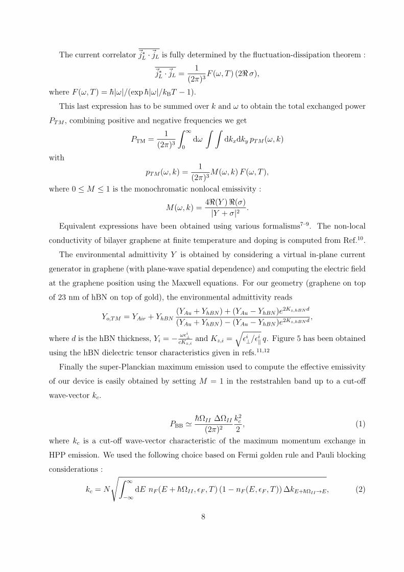
The current correlator j∗L · jL is fully determined by the fluctuation-dissipation theorem :
j∗L · jL =1
(2π)3F (ω, T ) (2ℜ σ),
where F (ω, T ) = h|ω|/(exp h|ω|/kBT − 1).
This last expression has to be summed over k and ω to obtain the total exchanged power
PTM , combining positive and negative frequencies we get
PTM =1
(2π)3
∫ ∞
0
dω
∫ ∫dkxdky pTM(ω, k)
with
pTM(ω, k) =1
(2π)3M(ω, k)F (ω, T ),
where 0 ≤ M ≤ 1 is the monochromatic nonlocal emissivity :
M(ω, k) =4ℜ(Y )ℜ(σ)|Y + σ|2
.
Equivalent expressions have been obtained using various formalisms7–9. The non-local
conductivity of bilayer graphene at finite temperature and doping is computed from Ref.10.
The environmental admittivity Y is obtained by considering a virtual in-plane current
generator in graphene (with plane-wave spatial dependence) and computing the electric field
at the graphene position using the Maxwell equations. For our geometry (graphene on top
of 23 nm of hBN on top of gold), the environmental admittivity reads
Yo,TM = YAir + YhBN(YAu + YhBN) + (YAu − YhBN)e
2Kz,hBNd
(YAu + YhBN)− (YAu − YhBN)e2Kz,hBNd,
where d is the hBN thickness, Yi = − ωϵi⊥cKz,i
and Kz,i =√ϵi⊥/ϵ
i∥ q. Figure 5 has been obtained
using the hBN dielectric tensor characteristics given in refs.11,12
Finally the super-Planckian maximum emission used to compute the effective emissivity
of our device is easily obtained by setting M = 1 in the reststrahlen band up to a cut-off
wave-vector kc.
PBB ≃ hΩII ∆ΩII
(2π)2k2c
2, (1)
where kc is a cut-off wave-vector characteristic of the maximum momentum exchange in
HPP emission. We used the following choice based on Fermi golden rule and Pauli blocking
considerations :
kc = N
√∫ ∞
−∞dE nF (E + hΩII , ϵF , T ) (1− nF (E, ϵF , T ))∆kE+hΩII→E, (2)
8

where nF is the Fermi distribution function, ∆kE1→E2 is the maximum wavevector exchanged
in the BLG bands when an electron transits from energy E1 to energy E2, and N is a
normalization factor given by
N =
√∫ ∞
−∞dE nF (E + hΩII , ϵF , T ) (1− nF (E, ϵF , T )).
The maximum energy relaxation rate par electron πPBB
k2F, for kc ≃ 2kF , defines an estimate
of the minimum emission time set by perfect electron coupling to the full HPP bandwidth
∆ΩII ≃ 30 meV,
τBB =hΩIIk
2F
πPBB
≃ 2π
∆ΩII
≃ 0.13 ps. (3)
1 C. R. Dean, A. F. Young, I.Meric, C. Lee, L. Wang, S. Sorgenfrei, K. Watanabe, T. Taniguchi,
P. Kim, K. L. Shepard, J. Hone, Nat. Nanotech. 5, 722 (2010). Boron nitride substrates for
high-quality graphene electronics
2 A.C. Betz, F. Vialla, D. Brunel, C. Voisin, M. Picher, A. Cavanna, A. Madouri, G. Feve, J-M.
Berroir, B. Placais, E. Pallecchi, Phys. Rev. Lett. 109, 056805 (2012). Hot electron cooling by
acoustic phonons in graphene.
3 A.C. Betz, S.H., Jhang, E. Pallecchi, R. Feirrera, G. Feve, J-M. Berroir, B. Placais, Nat. Phys.
9, 109 (2013). Supercollision cooling in undoped graphene.
4 M. F. Craciun, S. Russo, M. Yamamoto, J. B. Oostinga, A. F. Morpurgo and S. Tarucha, Nat.
Nano. 4, 383 (2009). Trilayer graphene is a semimetal with a gate-tunable band overlap
5 S. M. Rytov, Y. A. Kravtsov, V. I. Tatarskii, and A. P. Repyev, Springer (1989).
Principles of Statistical Radiophysics 3: Elements of Random Fields
6 A. I. Volokitin, and B. N. J. Persson, Reviews of Modern Physics, 79(4), 1291-1329. (2007).
Near-field radiative heat transfer and noncontact friction.
7 Y. Guo, C. L. Cortes, S. Molesky, and Z. Jacob Broadband super-Planckian thermal emission
from hyperbolic metamaterials Applied Physics Letters, bf 101(13) (2012)
8 Y. Guo, and Z. Jacob, Journal of Applied Physics, 115(23), 234306 (2014). Fluctuational elec-
trodynamics of hyperbolic metamaterials.
9 A. Principi, M. B. Lundeberg, N.C.H. Hesp, K-J. Tielrooij, F.H.L. Koppens, M.Polini, Phys.
Rev. Lett. 118, 126804 (2017) Super-Planckian electron cooling in a van der Waals stack
9

10 T. Low, F. Guinea, H. Yan, F. Xia, and P. Avouris, Physical Review Letters, 112(11), 1-5.
(2014). Novel midinfrared plasmonic properties of bilayer graphene
11 A. Kumar, T. Low, K. H. Fung, P. Avouris, and N. X. Fang, Nano Letters, 15(5), 3172-3180
(2015). Tunable light-matter interaction and the role of hyperbolicity in graphene-hbn system
12 Y. Cai, L. Zhang, Q. Zeng, L. Cheng, and Y. Xu, Solid State Comm. 141(5), 262-266. (2007)
Infrared reflectance spectrum of BN calculated from first principles
13 N. Meric, M. Y. Han, A. F. Young, B.A. Ozylmaz, P. Kim, K. L. Shepard, Nat. Nanotech. 3,
654 (2008). Current saturation in zero-bandgap, topgated graphene field-effect transistors
14 J. Yan, Y. Zhang, P. Kim, A. Pinczuk, Phys. Rev. Lett. 98, 166802 (2007) Electric Field Effect
Tuning of Electron-Phonon Coupling in Graphene
10
A graphene Zener-Klein transistor cooled by a hyperbolic
substrate. (supplementary)
Wei Yang, Simon Berthou, Xiaobo Lu, Quentin Wilmart, Anne Denis, Michael
Rosticher, Takashi Taniguchi, Kenji Watanabe, Gwendal Feve, Jean-Marc Berroir,
Guangyu Zhang, Christophe Voisin, Emmanuel Baudin, and Bernard Placais
1

Cu
rre
nt
no
ise
(p
A2/H
z)
0
50
100
150
Frequency (GHz)
0 2 4 6 8 10
0.5V
1.5V
2.5V
3.5V
a b
FIG. S-1: Panel a) : scheme of the measuring set-up. Panel b) : typical current noise spectrum
measured in the 0–10 GHz band width.
I. EXPERIMENTAL SETUP AND NOISE CALIBRATION
A schematic of our noise thermometry setup is illustrated in Figure S-1-a. The principle
is derived from the 0–1 GHz setup of Ref.2 which has been upgraded to the 0–10 GHz
bandwidth to overcome the 1/f -noise at the ultimate currents of our experiment. The
graphene sample, embedded in a coplanar wave guide, is enclosed in a compact sample
holder enclosed in a 40 GHz (Southwest Microwave) end launch connector. The RF output
is 50 Ohms adapted to secure a broadband matching to the 12 GHz bandwidth (Caltech)
cryogenic low noise amplifier (LNA) (FigureS-1-a). Two capacitors (C ∼ 1 nF) are used
to decouple DC and RF signals. The power gain is calibrated against the shot-noise of a
Al/Al2O3/Al tunnel junction. The background noise, consisting of the equilibrium thermal
noise at 4.2 K and the excess noise (≃ 4 K) of the LNA, are subtracted from zero bias voltage
measurement. Three spurious resonances are observed in the noise spectra of FigureS-1-b
(shaded area in the figure) which are due to non-ideality of the biasing components; for
accurate measurement of the current noise we have restricted ourself to the 4.5–5.5 GHz
bandwidth.
II. PERFORMANCE OF THE BILAYER GRAPHENE ZENER-KLEIN TUNNEL-
ING TRANSISTOR
The transconductance and voltage gain are shown in Figs. S-2-c and d. For completeness
we have reproduced the data of Fig.1 (main text) in panels -a and -b. Transconductance
2

Drain
Source
R (
kΩ
)
0
5
10
15
Vgs (V)
−6 −4 −2 0 2 4 6
10
100
1 000
10 000
−5 0 5
J (A
/mm
)
0
0.5
1
1.5
2
2.5
Vds (V)
0 1 2 3 4 5
0V
1V
2V
3V
4V
5V
6V
7V
dIds/dVgs (mS)Voltage Gain
a b
dc
FIG. S-2: Bottom-gated bilayer graphene on hBN transistor (optical image in panel a-inset). a)
Low-bias transfer curve R = 1/gds measured at 4 Kelvin and Vds = 10 mV. A logarithmic plot
(inset) shows the small contact resistance in the hole side and a larger one in the electron-side due
to contact doping. The bilayer nature of the sample and the gate capacitance Cg = 1.15 mS/m2
are deduced from independent quantum Hall measurements (not shown), from which we infer a
mobility µ ≃ 3.104cm2V−1s−1. b) current saturation for different gate voltages in the electron
doped regime (positive bias). Panels c), d), transconductance gm = ∂I/∂Vgs|Vdsand voltage gain
G = gm/gds as a function of gate and drain voltages. gm saturates at ±0.8 mS and changes sign
along the line Vgs ≃ 0.4Vds. The gain peaks at large values (G ≃ 10) at high bias and high doping
(Vds, Vgs ≥ 4 V).
saturates at gm = ±250 mS/mm and voltage gain peaks at G ≃ 10 at large bias13. These
figures show that this sample reaches the ultimate performances allowed by the intrinsic
properties of graphene. As seen in panel -c, the transconductance vanishes along a line
Vg ≃ 0.4Vd (charge neutrality in the channel) reflecting a geometrical correction due to the
near vicinity of the gate electrode. From that line we deduce the average channel doping,
ne = CgsVgs + CgdVgd ≃ Cg(Vgs − 0.4Vds). The full current saturation at higher doping
actually results, with a differential conductivity σ = σzk − CgdvsatL ≃ 0 in our 4 µm-long
samples, from the balance of the ZKT current by a decrease of the intraband saturation
current due to the pinching of the carrier density when increasing Vds at constant Vgs at the
electron side.
3

0
50
V ds (V )
0 0,2 0,4J
(A/m
m)
0
1
2
E (V/µm)
0 0,2 0,4 0,6 0,8
kB
T (
eV
)
0
0,1
0,2
0,3
E (V/µm)
0 0,2 0,4 0,6 0,8
a b
0
0,02
V ds (V )
0 0,2 0,4
J (A
/mm
)
0
0,4
0,8
1,2
1,6
2
2,4
E (V/µm)
0 0,5 1 1,5
kB
TN
(e
V)
0
0,05
0,1
0,15
0,2
E (V/µm)
0 0,5 1 1,5
c d
n
n
n
n
FIG. S-3: Current and noise saturation in single-layer (a and b) and tri-layer (c and d) graphene
Zener-Klein transistors in the hole doped regime. General behavior is similar to the BLG data
analyzed in detail in the main text. The insets show the Vds = 0.2 V threshold for HPP emission
at charge neutrality.
III. MONOLAYER AND TRILAYER GRAPHENE TRANSISTORS
The electrical performance of single layer graphene (SLG) and trilayer (TLG) devices
are shown in Figure S-3. SLG and TLG sample dimensions are L × W = 10 × 3 µm and
L ×W = 2.5 × 2 µm respectively and an hBN thickness of 20 nm and 43 nm respectively.
The high-field transport and noise properties are measured at constant carrier density for
Vgs = −7 7→ 0 V and Vgs = −8 7→ 0 V respectively. They are qualitatively similar to
those of the BLG device in the main text with both current and noise saturation in the
Zener-Klein regime. The Zener-Klein conductances are σSLGzk ≃ 1.2 mS and σTLG
zk ≃ 2 mS.
Differences with the BLG sample of the main text come from a lower mobility and a lower
current saturation level. These samples do not reach the intrinsic limits and are therefore
less prone to a quantitative analysis. A more fundamental difference comes from the density
4

of state which is energy dependent in SL and TL graphene. Remarkably the SLG and
TLG samples show an onset for HPP emission at Vds = 0.2 V, similar to that of the BLG
sample, indicative of an HPP energy hΩII ≃ 0.2 eV. The Wiedemann-Franz cooling regime
is observed in the SLG sample whereas the low bias regime in the TLG sample deviates
from a pure WF cooling regime, presumably due to a more prominent contribution of HPP
emission in the hot electron regime. An in-depth analysis of HPP emission by SLG and
TLG will be reported elsewhere.
J (A
/mm
)
0
1
2
0 0.25 0.5 0.75 1 1.25
0
0.1
0.2
0.3
0.4
E (V/µm)0 0.25 0.5 0.75 1
J (A
/mm
)
0
1
2
0 0.25 0.5 0.75 1 1.250.0
0.1
0.2
0.3
0.4
0 0.25 0.5 0.75 1
E (V/µm)
E (V/µm) E (V/µm)
No
ise
te
mp
era
ture
(e
V)
No
ise
te
mp
era
ture
(e
V)
a
c
b
d
(CNP)
(CNP)
FIG. S-4: Comparison of the transport and noise temperature characteristics of two bilayer tran-
sistors with an hBN dielectric thickness of 23 nm (panels a,b) and 200 nm (panels c,d). The
two devices have quasi identical dimensions (L × W ≃ 4 × 3 µm) and the hole carrier density is
incremented from p = 0 (black line) to p = 2.1012 cm−2 (full green line).
IV. EFFECT OF HBN THICKNESS IN BILAYER GRAPHENE TRANSISTORS
Figure S-4 shows a comparison of transport and noise properties of between the BLG
sample of the main text of dimensions L × W ≃ 4 × 3 µm and hBN thickness t = 23 nm
(panels a,b) and a similar one with L×W ≃ 3.6× 3 µm and t = 200 nm (panels c, d). The
5

color code for the (hole) carrier density is unified for both samples from p = 0 (black line)
to p = 2.1012 cm−2 (full green line) with an increment ∆p ≃ 7.1011 cm−2.
The transport and noise characteristics of the two samples are qualitatively similar. They
have a similar mobility and saturation currents and noise thermometry carry the same qual-
itative features. Concerning transport (panels a,c), the main differences of the thick hBN
sample are a negligible drain gating effect and a decrease of the Zener-Klein conductance
αZK , presumably due to smoother Zener-Klein junctions (smaller αZK). The later is re-
sponsible for a decrease of the total Joule power and an overbalance of Joule power by HPP
cooling. The noise temperature in the ZKT regime is very similar in the two samples indi-
cating that the ZKT e-h pair creation is indeed independent of the transparency αZK , and
constitutes an absolute lower limit for the noise of ZKT transistors.
FIG. S-5: Ratio of the anti-Stokes integrated amplitude by the Stokes integrated amplitude (red)
and of the measured surface Joule power (blue) function of the applied electric field for a gate
voltage of -4 V (taking into account self-gating).
V. OPTICAL PHONON RAMAN SPECTROSCOPY
We performed anti-Stokes (AS) Raman scattering spectroscopy to investigate the role
of the electron-intrinsic graphene’s OP coupling in the cooling of the electron gas. Using
a He-Ne laser, we monitored the intensities of the Stokes and anti-Stokes lines of the G
mode as a function of the bias voltage. In the low temperature limit, this ratio yields
6

the occupation number of the OP mode at the Γ point of the Brillouin zone. In order
to account for the spectral detectivity of our setup, this ratio was calibrated against room
temperature measurements where the AS line is detectable for an integration time of 15 min.
The uncertainties have been carefully evaluated from the standard deviation of the detected
noise nearby the AS line. Fig. S-5 shows that the occupation number remains below the
detection limit at low bias and reaches a value of the order of 0.01 at high bias. We first note
that there is no coincidence between the E-field range where the AS line becomes significant
(E > 0.6 V/m) and the ZKT threshold field (Ezk > 0.25 V/m) at which the the cooling
power dramatically increases according to Fig.2-c (main text).
We estimated a maximum value for the cooling power due to the graphene intrinsic OPs by
considering a conservative OP lifetime of 1 ps consistent with experimental measurements14
and a very conservative band occupation up to kc <∼ 1.38 nm−1 (found using Eq. 2). The
measured AS to S ratio shows that the coupling of electrons to OPs represents less than 25%
of the total Joule power emitted by the electrons at the maximum electric field (∼ 1 V.µm−1)
thus ruling out intrinsic OP cooling as the main cooling mechanism of graphene’s electrons.
VI. COMPUTATION OF THE SUPER-PLANCKIAN EMISSION
Fluctuation electrodynamics5,6 allows us to compute the super-Planckian emission of BLG
in its environment. In this context, each plane-wave mode of graphene is a current generator
of amplitude js, where s designates the longitudinal or transverse character of the current
generator. In super-Planckian emission, the power is mainly cast via the TM polarization
modes and consequently we will only consider the longitudinal currents. This generator emits
power in the graphene which has an impedance σ−1, where σ is the optical conductivity of
graphene, and in its electromagnetic environment which has an impedance Z = Y −1, where
Y is the admitivity (far field and near field) of the electromagnetic environment of the
graphene layer. The power radiated by the graphene electrons is equal to the dissipation in
the electromagnetic environment only, and is computed via
pTM = −ℜ (jL + σETM)∗.ETM =ℜ(Y )
|Y + σ|2j∗L · jL
.
7

The current correlator j∗L · jL is fully determined by the fluctuation-dissipation theorem :
j∗L · jL =1
(2π)3F (ω, T ) (2ℜ σ),
where F (ω, T ) = h|ω|/(exp h|ω|/kBT − 1).
This last expression has to be summed over k and ω to obtain the total exchanged power
PTM , combining positive and negative frequencies we get
PTM =1
(2π)3
∫ ∞
0
dω
∫ ∫dkxdky pTM(ω, k)
with
pTM(ω, k) =1
(2π)3M(ω, k)F (ω, T ),
where 0 ≤ M ≤ 1 is the monochromatic nonlocal emissivity :
M(ω, k) =4ℜ(Y )ℜ(σ)|Y + σ|2
.
Equivalent expressions have been obtained using various formalisms7–9. The non-local
conductivity of bilayer graphene at finite temperature and doping is computed from Ref.10.
The environmental admittivity Y is obtained by considering a virtual in-plane current
generator in graphene (with plane-wave spatial dependence) and computing the electric field
at the graphene position using the Maxwell equations. For our geometry (graphene on top
of 23 nm of hBN on top of gold), the environmental admittivity reads
Yo,TM = YAir + YhBN(YAu + YhBN) + (YAu − YhBN)e
2Kz,hBNd
(YAu + YhBN)− (YAu − YhBN)e2Kz,hBNd,
where d is the hBN thickness, Yi = − ωϵi⊥cKz,i
and Kz,i =√ϵi⊥/ϵ
i∥ q. Figure 5 has been obtained
using the hBN dielectric tensor characteristics given in refs.11,12
Finally the super-Planckian maximum emission used to compute the effective emissivity
of our device is easily obtained by setting M = 1 in the reststrahlen band up to a cut-off
wave-vector kc.
PBB ≃ hΩII ∆ΩII
(2π)2k2c
2, (1)
where kc is a cut-off wave-vector characteristic of the maximum momentum exchange in
HPP emission. We used the following choice based on Fermi golden rule and Pauli blocking
considerations :
kc = N
√∫ ∞
−∞dE nF (E + hΩII , ϵF , T ) (1− nF (E, ϵF , T ))∆kE+hΩII→E, (2)
8
where nF is the Fermi distribution function, ∆kE1→E2 is the maximum wavevector exchanged
in the BLG bands when an electron transits from energy E1 to energy E2, and N is a
normalization factor given by
N =
√∫ ∞
−∞dE nF (E + hΩII , ϵF , T ) (1− nF (E, ϵF , T )).
The maximum energy relaxation rate par electron πPBB
k2F, for kc ≃ 2kF , defines an estimate
of the minimum emission time set by perfect electron coupling to the full HPP bandwidth
∆ΩII ≃ 30 meV,
τBB =hΩIIk
2F
πPBB
≃ 2π
∆ΩII
≃ 0.13 ps. (3)
1 C. R. Dean, A. F. Young, I.Meric, C. Lee, L. Wang, S. Sorgenfrei, K. Watanabe, T. Taniguchi,
P. Kim, K. L. Shepard, J. Hone, Nat. Nanotech. 5, 722 (2010). Boron nitride substrates for
high-quality graphene electronics
2 A.C. Betz, F. Vialla, D. Brunel, C. Voisin, M. Picher, A. Cavanna, A. Madouri, G. Feve, J-M.
Berroir, B. Placais, E. Pallecchi, Phys. Rev. Lett. 109, 056805 (2012). Hot electron cooling by
acoustic phonons in graphene.
3 A.C. Betz, S.H., Jhang, E. Pallecchi, R. Feirrera, G. Feve, J-M. Berroir, B. Placais, Nat. Phys.
9, 109 (2013). Supercollision cooling in undoped graphene.
4 M. F. Craciun, S. Russo, M. Yamamoto, J. B. Oostinga, A. F. Morpurgo and S. Tarucha, Nat.
Nano. 4, 383 (2009). Trilayer graphene is a semimetal with a gate-tunable band overlap
5 S. M. Rytov, Y. A. Kravtsov, V. I. Tatarskii, and A. P. Repyev, Springer (1989).
Principles of Statistical Radiophysics 3: Elements of Random Fields
6 A. I. Volokitin, and B. N. J. Persson, Reviews of Modern Physics, 79(4), 1291-1329. (2007).
Near-field radiative heat transfer and noncontact friction.
7 Y. Guo, C. L. Cortes, S. Molesky, and Z. Jacob Broadband super-Planckian thermal emission
from hyperbolic metamaterials Applied Physics Letters, bf 101(13) (2012)
8 Y. Guo, and Z. Jacob, Journal of Applied Physics, 115(23), 234306 (2014). Fluctuational elec-
trodynamics of hyperbolic metamaterials.
9 A. Principi, M. B. Lundeberg, N.C.H. Hesp, K-J. Tielrooij, F.H.L. Koppens, M.Polini, Phys.
Rev. Lett. 118, 126804 (2017) Super-Planckian electron cooling in a van der Waals stack
9

10 T. Low, F. Guinea, H. Yan, F. Xia, and P. Avouris, Physical Review Letters, 112(11), 1-5.
(2014). Novel midinfrared plasmonic properties of bilayer graphene
11 A. Kumar, T. Low, K. H. Fung, P. Avouris, and N. X. Fang, Nano Letters, 15(5), 3172-3180
(2015). Tunable light-matter interaction and the role of hyperbolicity in graphene-hbn system
12 Y. Cai, L. Zhang, Q. Zeng, L. Cheng, and Y. Xu, Solid State Comm. 141(5), 262-266. (2007)
Infrared reflectance spectrum of BN calculated from first principles
13 N. Meric, M. Y. Han, A. F. Young, B.A. Ozylmaz, P. Kim, K. L. Shepard, Nat. Nanotech. 3,
654 (2008). Current saturation in zero-bandgap, topgated graphene field-effect transistors
14 J. Yan, Y. Zhang, P. Kim, A. Pinczuk, Phys. Rev. Lett. 98, 166802 (2007) Electric Field Effect
Tuning of Electron-Phonon Coupling in Graphene
10