A glimpse of MEMS - Penn Engineeringmeam550/fall2001/notes2001/MEAM550intro.pdf · A glimpse of...
57
G.K. Ananthasuresh, U. of Pennsylvania, Sep. 2001 Mechanical Engineering and Applied Mechanics University of Pennsylvania A glimpse of MEMS G. K. Ananthasuresh September 17, 2001 Presented to MEAM 550 (Fall 2001) students
Transcript of A glimpse of MEMS - Penn Engineeringmeam550/fall2001/notes2001/MEAM550intro.pdf · A glimpse of...

G.K. Ananthasuresh, U. of Pennsylvania, Sep. 2001
Mechanical Engineering and Applied MechanicsUniversity of Pennsylvania
A glimpse of MEMS
G. K. AnanthasureshSeptember 17, 2001
Presented to MEAM 550 (Fall 2001) students

G.K. Ananthasuresh, U. of Pennsylvania, Sep. 2001
What’s in a name?
� Micro-Electro-Mechanical Systems (MEMS)Widely used in Americas.
� MicroSystems Technology (MST)Popular in Europe.
� MicromachinesUsed in Japan.
� MicroscienceSome people prefer to call it this way as they begin to explore scientific aspects of MEMS.

G.K. Ananthasuresh, U. of Pennsylvania, Sep. 2001
Outline
� What are they?� How small are they?� How are they useful?� How do they work?� What are they made of?� How are they made?� How do you design them?� What are the modeling and design issues
and challenges for us?

G.K. Ananthasuresh, U. of Pennsylvania, Sep. 2001
A MEMS design question
What does this mean?
1. MEMS field is somewhat mature because people are asking routine questions about how to design them.
2. There must be something different about designing them.
3. There is a need to learn the basics of the field and be familiar with the jargon of the field.
And so we begin…

G.K. Ananthasuresh, U. of Pennsylvania, Sep. 2001
What are they?
� MEMS are systems that integrate…� sensing� actuation� computation� control� communication� power They are…
smallermore functionalfasterless power-consuming
and cheaper!

G.K. Ananthasuresh, U
. of Pennsylvania, Sep. 2001
How
small are they?
0A1 nm
0.1 um10 um
1 mm
100 mm
10 m
10 nm1 um
100 um10 m
m1 m
Atoms
MoleculesDNA
NanostructuresVirus
Smallest micro-electronic features
Nanotechnology
Microsystem
sM
esoM
acrosystems
BacteriaBiological cellsDust particles
Dia. of human hair
MEMS Optical fibers
Packaged ICsPackaged MEMSLab-on-a-chip
Plain old machinesHumansAnimalsPlamtsPlanes, trains, and automobiles
Precision machining
Nano-m
achiningM
icro-machining
Macro-m
achining

G.K. Ananthasuresh, U. of Pennsylvania, Sep. 2001
Why are they small?
“Micro” size is almost incidental.
� They are small because of the technologies used to make them.
� And it is economical to make them small –when made in large volumes just like microelectronics.
� Of course, there are some MEMS devices that would not work if they are any bigger.

G.K. Ananthasuresh, U. of Pennsylvania, Sep. 2001
A bit of history…
� “There is plenty of room at the bottom”- A 1959 lecture by Richard Feynman
� Pioneered by Professor James Angell at Stanford University, researchers at Westinghouse in late 1960’s into 1970’s
� “Infinitesimal Machinery”- A 1983 lecture by Richard Feynman
� Formal identity (“MEMS”) to the field came in late1980’s

G.K. Ananthasuresh, U. of Pennsylvania, Sep. 2001
What (more) are they?
Solid state transducers MEMSEarly on…
And later…
Integrated systems
sensorsactuators
• are batch fabricated• are economical• have more functionality• involve physical, chemical, biochemical phenomena at small scales• act upon macro scale too
Take leverage of the enormously successful VLSI technology

G.K. Ananthasuresh, U. of Pennsylvania, Sep. 2001
How are they useful
� Pressure sensors� Accelerometers� Ink-jet printer heads� Projection display with micro mirror array� Portable clinical analyzers� etc.
Movable solids and fluids at microscale made possiblelots and lots of sensors and actuators.
Commercial successes

G.K. Ananthasuresh, U. of Pennsylvania, Sep. 2001
More applications
� Inertial measurement devices� Accelerometers, gyroscopes
� Mass data storage� Opto-mechanical devices
� Projection displays, photonics, optics-on-a-chip
� Flow control� Bio-chemical lab-on-a-chip� Communication hardware
� Mechanical filters, RF-switches and relays
� Chemical microreactors� Power MEMS
� Micro engines, generators

G.K. Ananthasuresh, U. of Pennsylvania, Sep. 2001
A slide from DARPA-MTO website

G.K. Ananthasuresh, U. of Pennsylvania, Sep. 2001
A slide from DARPA web siteUCLA
MEMS creating large effects – an example

G.K. Ananthasuresh, U. of Pennsylvania, Sep. 2001
A slide from DARPA-MTO web site
Towards lab-on-a-chip
Bio-flips

G.K. Ananthasuresh, U. of Pennsylvania, Sep. 2001
A slide from DARPA-MTO web site
Impact on the health-care

G.K. Ananthasuresh, U. of Pennsylvania, Sep. 2001
Outline
� What are they?� How small are they?� How are they useful
� How do they work?
Pressure sensor
V
Capacitive sensing Piezoresistive sensing

G.K. Ananthasuresh, U. of Pennsylvania, Sep. 2001
How do they work?
V
Accelerometer
Side view
Top view

G.K. Ananthasuresh, U. of Pennsylvania, Sep. 2001
How do they work?
torsional beam
actuating electrode 1
Tiltablemirror
torsional beam
actuating electrode 2
TI’s digital light processor

G.K. Ananthasuresh, U. of Pennsylvania, Sep. 2001
What lies beneathTI’s digital light processor (DLP) and deformable mirror display (DMD)
Ant’s leg on the DMD array
Anatomy of DLP/DMD

G.K. Ananthasuresh, U. of Pennsylvania, Sep. 2001
How do they work
Ink-jet printer head
“drive” air bubble
ejectedink dropletWeight: ng
paper
resistive heater
orifice
�Electronics are integrated to trigger the drive bubble

G.K. Ananthasuresh, U. of Pennsylvania, Sep. 2001
How do they work?
A mechanical relay
V
Dielectric
Signal input
Signal output

G.K. Ananthasuresh, U. of Pennsylvania, Sep. 2001
How do they work?
A normally closed fluidic valve
FlowGlass
Trapped fluid Glass
Silicon
(Redwood Microsystems)

G.K. Ananthasuresh, U. of Pennsylvania, Sep. 2001
How do they work?
V
A diaphragm pump
Diaphragm
Passive inlet valve Passive outlet valve

G.K. Ananthasuresh, U. of Pennsylvania, Sep. 2001
Outline
� What are they?� How small are they?� How are they useful� How do they work?
� What are they made of?� How are they made?

G.K. Ananthasuresh, U. of Pennsylvania, Sep. 2001
What are they made of?
Phase 1: Old materials and old processesSilicon, its oxide, nitride, and some metalsIC-chip processing technology
LithographyThin film deposition (e.g., chemical vapor deposition – CVD)EtchingDoping
Phase 2: Old materials and new processesSilicon, its oxide, nitride, glass, polysilicon, and some metalsIC-chip processing techniques enhanced as “micromachining” techniquesSacrificial layer process
Deep reactive ion etchingLIGA HexilDissolved wafer process
Etc.Wafer bonding

G.K. Ananthasuresh, U. of Pennsylvania, Sep. 2001
What are they made of (contd.)
Phase 3: New materials and old processesPolymersMore metalsCeramicsSilicon carbidePiezoelectric filmsFerroelectric filmsShape-memory materials, etc.
Phase 4: New materials and new processesProcesses unconventional to the microelectronic fieldProcesses that re-define the size of MEMS – micro to meso or nanoDeposition and etching for the new materials
e.g., PDMSGeorge Whitesides at Harvard
G.K. Ananthasuresh, U. of Pennsylvania, Sep. 2001
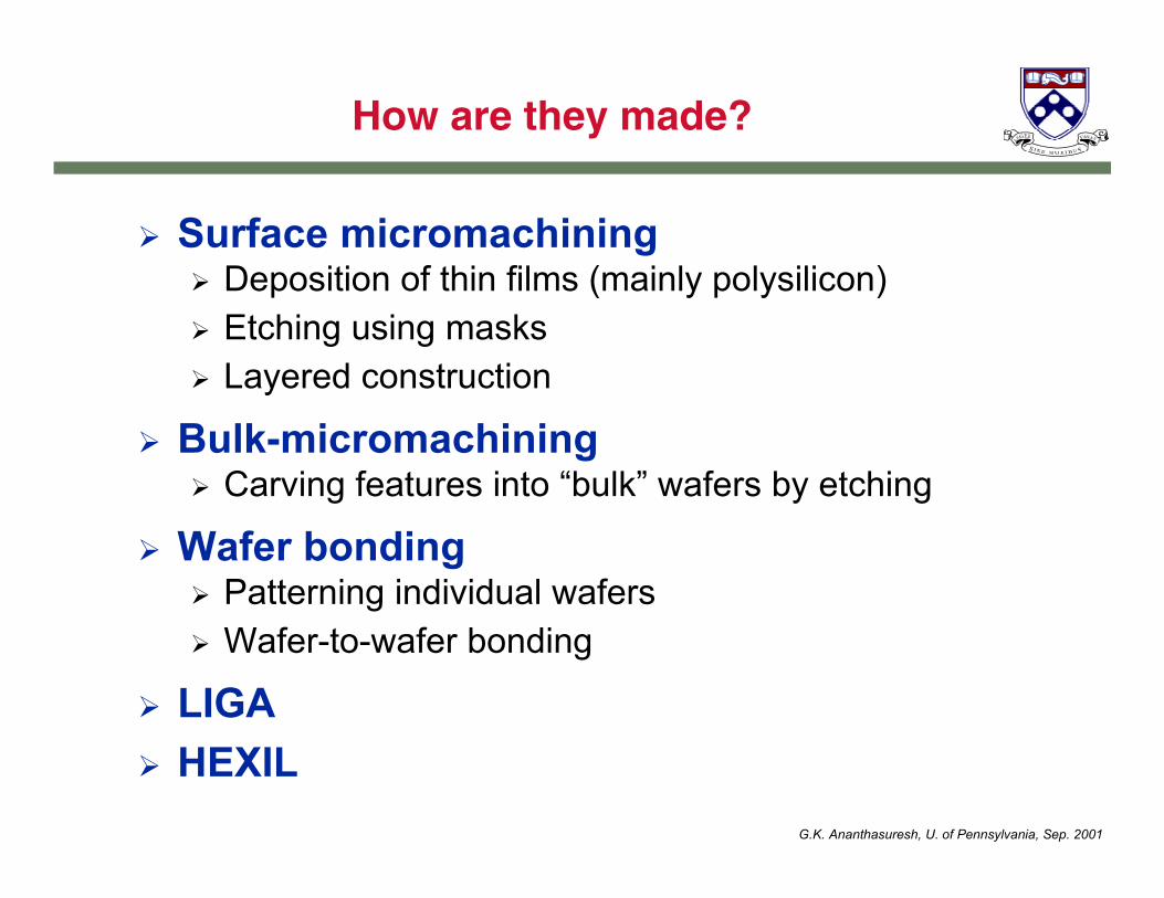
How are they made?
� Surface micromachining� Deposition of thin films (mainly polysilicon)� Etching using masks� Layered construction
� Bulk-micromachining� Carving features into “bulk” wafers by etching
� Wafer bonding� Patterning individual wafers� Wafer-to-wafer bonding
� LIGA� HEXIL

G.K. Ananthasuresh, U. of Pennsylvania, Sep. 2001
Micromachining is not precision machining!
Precision machining � Relative tolerance (feature to part size) is better than 10-4.
For micromachinig, it is 10-2 to 10-3.Roughly what we have for building houses.
With micromachining,
You can make it small, but not precisely.(at least not yet. Wait for nanotechnology…)
G.K. Ananthasuresh, U. of Pennsylvania, Sep. 2001
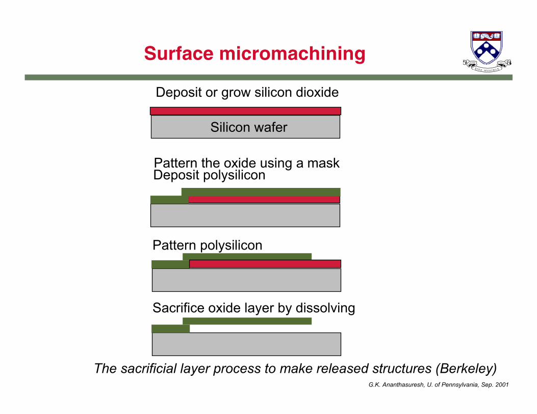
Surface micromachining
Silicon wafer
Deposit or grow silicon dioxide
Pattern the oxide using a maskDeposit polysilicon
Pattern polysilicon
Sacrifice oxide layer by dissolving
The sacrificial layer process to make released structures (Berkeley)
G.K. Ananthasuresh, U. of Pennsylvania, Sep. 2001
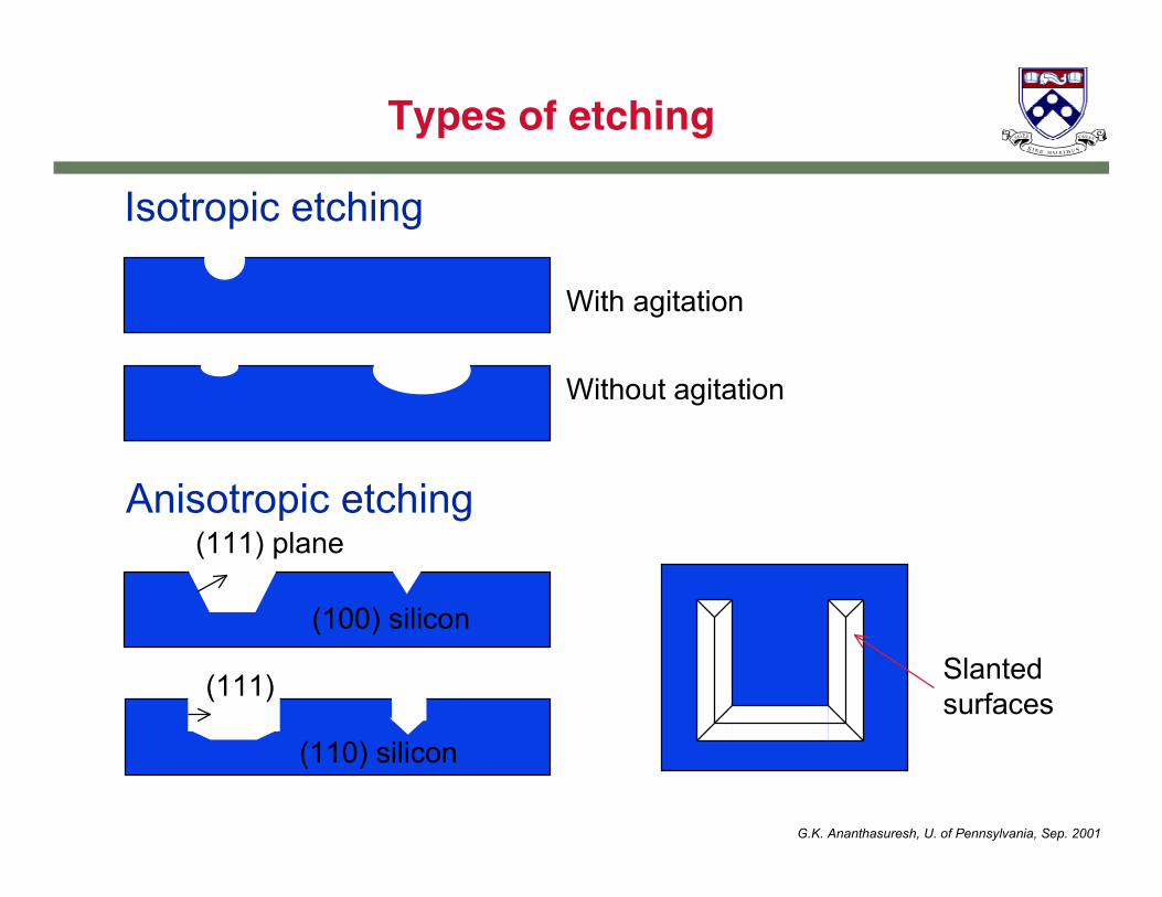
Types of etching
(100) silicon
(110) silicon
(111) plane
(111)
With agitation
Without agitation
Isotropic etching
Anisotropic etching
Slantedsurfaces

G.K. Ananthasuresh, U. of Pennsylvania, Sep. 2001
Bulk micromachining
Silicon wafer
Etch using a mask
Boron doping using a mask
Dissolve undoped silicon
Boron doped dissolved wafer process (Michigan)
Flip and bond to a glass
Glass

G.K. Ananthasuresh, U. of Pennsylvania, Sep. 2001
Wafer bonding
Etch a cavity in a wafer
Thin down / polish and etch
Bond another wafer
Released cantilever using MIT’s wafer bonding process

G.K. Ananthasuresh, U. of Pennsylvania, Sep. 2001
Making an electrostatic micromotorusing surface micromachining
Cronos MUMPs (formerly MCNC MUMPs)
Stator poles
Rotor
Top view
Side view
After sacrificing oxide layers…

G.K. Ananthasuresh, U. of Pennsylvania, Sep. 2001
Making a micromotor
Deposit poly0 Etch poly0 Deposit oxide1
Dimples in oxide1 Etch oxide1 Deposit poly1

G.K. Ananthasuresh, U. of Pennsylvania, Sep. 2001
Making a micromotor (contd.)
Etch poly1 Deposit oxide2
Cross-section up to this point…
Cronos MUMPs (formerly MCNC MUMPs)

G.K. Ananthasuresh, U. of Pennsylvania, Sep. 2001
Making the micromotor (contd.)
Etch oxide2 Deposit poly2 Etch poly2
Deposit and etch metal
Cross-section before sacrificing oxide layersCronos MUMPs (formerly MCNC MUMPs)

G.K. Ananthasuresh, U. of Pennsylvania, Sep. 2001
Finished micromotor

G.K. Ananthasuresh, U. of Pennsylvania, Sep. 2001
Micromotor after “release”
Cronos MUMPs (formerly MCNC MUMPs)

G.K. Ananthasuresh, U. of Pennsylvania, Sep. 2001
How much should we know about u-fab?
www.seas.upenn.edu/~meam550

G.K. Ananthasuresh, U. of Pennsylvania, Sep. 2001
Visualize device from a verbal description of the process
Being able to draw the process flow diagrams from a description.
Shallow pits were etched into n-type substrates, and p-type deflection electrodes were diffused in the above pits, followed by fusion bonding of a second wafer above the first. The top wafer was then ground and polished down to a thickness of 6 um. A passivation layer was then formed on the top wafer and sensing piezoesistors were formed using ion implantation, after which contact holes for metallization to connect to he diffused deflection electrodes were etched. Bond pads and interconnect metallization were then deposited and patterned, followed by etching of the diaphragm from the back of the wafer. Finally, two slots were etched next to the beam to release it over the buried cavity. (Petersen et al., 1991)
See http://www.seas.upenn.edu:8080/~meam550/solution2.html

G.K. Ananthasuresh, U. of Pennsylvania, Sep. 2001
Visualize the process steps from a device cross section
Visualizing a process from a cross-section.
How was this made?See http://www.seas.upenn.edu:8080/~meam550/solution2.html

G.K. Ananthasuresh, U. of Pennsylvania, Sep. 2001
MEMS Foundries
Cronos MUMPs (formerly MCNC’s MUMPs)Now, owned and operated by Uniphase.
You don’t have to make them if you don’t want to or can’t.

G.K. Ananthasuresh, U. of Pennsylvania, Sep. 2001
Making elements of mechanisms
A surface micromachined hinge(Kris Pister, Berkeley)
Substrate hinge

G.K. Ananthasuresh, U. of Pennsylvania, Sep. 2001
Floating hinges
Masklayout

G.K. Ananthasuresh, U. of Pennsylvania, Sep. 2001
Electrostatic comb drive
anchorShuttlemass
Folded-beam suspension Movingcombs
Fixedcombs
Misaligned comb capacitors align creating actuation.

G.K. Ananthasuresh, U. of Pennsylvania, Sep. 2001
Sandia’s micro mechanical lock
Pin in a maze

G.K. Ananthasuresh, U. of Pennsylvania, Sep. 2001
Close-up of Sandia’s micro lock

G.K. Ananthasuresh, U. of Pennsylvania, Sep. 2001
Merry go-around for mites
See Sandia’s web site for animation

G.K. Ananthasuresh, U. of Pennsylvania, Sep. 2001
Sandia’s SUMMiT process revolute joint
Substrate
Pin
Rotor

G.K. Ananthasuresh, U. of Pennsylvania, Sep. 2001
Deep etching
Deep RIE (reactive ion etching) to get vertical sidewalls over large depths of several hundred microns.
E.g., SCREAM (Cornell) bulk-micromachining

G.K. Ananthasuresh, U. of Pennsylvania, Sep. 2001
SCREAM process
Deposit and pattern mask oxide
Deep RIE silicon etch
Deposit sidewall oxide
Etch bottom sidewall oxide
Second deep RIE silicon etch
Isotropic silicon etch
Noel MacDonald, Cornell university

G.K. Ananthasuresh, U. of Pennsylvania, Sep. 2001
Packaging!
Packaging is a big problem with MEMS. Sometimes, it may be better not integrate sensor/actuator and electronics.
Signal redistributionMechanical supportPower distributionThermal managementFluidic fittingsEtc.
Packaging � access to and protection from the external macro world
Ball and wire bondingFlip-chipSandia’s processResearch continues…
Packaging serves…
Some techniques

G.K. Ananthasuresh, U. of Pennsylvania, Sep. 2001
Outline
� What are they?� How small are they?� How are they useful� How do they work?� What are they made of?� How are they made?
� How do you design them?� What are the modeling and design issues
and challenges for us?

G.K. Ananthasuresh, U. of Pennsylvania, Sep. 2001
Modeling and design of MEMS –What is different?
Integration of sensor, actuator, mechanism, processor, power, and communication makes system level tasks challenging
-- common representation for multiple energy domains
Device level too has multiple energy domains-- macromodels
Component level-- coupled energy domain equations
Mask level-- geometric modeling

G.K. Ananthasuresh, U. of Pennsylvania, Sep. 2001
Modeling and design of MEMS
System
Device
Component(physical)
Artwork of masksand process
Each level involves designThere is “analysis” (forward) problem and “synthesis” (inverse) problem.
Representing as block diagrams of multi-domain subsystems
Reduced order “macro models” of the components
Multiple, coupled energy behavioral simulations
Defining mask geometry for the process steps

G.K. Ananthasuresh, U. of Pennsylvania, Sep. 2001
The future of MEMS?
The proverb:
Forecasting is difficult, especially the future.(from Chinese fortune cookies)
In any case, MEMS will impact the following industries:
AutomotiveAerospaceBiomedical/bio-techHealth-careTelecommunicationInformation technology

G.K. Ananthasuresh, U. of Pennsylvania, Sep. 2001
Further reading
�Principles of microfabrication – Marc Madou
�Micromachined transducers: A source book – Greg Kovacs
�Microsystem Design – Steve Senturia
�MEMS: Advanced materials and fabrication methods – National Research Council (NRC)
committee report, 1997
�An Introduction to Microelectromechanical Systems Engineering – N. Maluf
�Microsensors – J. W. Gardner
�Sensor Technology and Devices – L. Ristic
�Transducers, Sensors, and Detectors – R. G. Seippel
�Microactuators: Electrical, Magnetic, Thermal, Optical, Mechanical, Chemical, and Smart
Structures – M. Tabib-Azar
�Nano- and Microelectromechanical Systems: Fundamentals of Nano- and
Microengineering – S. E. Lyshevski
Books