A Differential Complementary Colpitts Oscillator based on ... · A Differential Complementary...
4
A Differential Complementary Colpitts Oscillator based on Common Drain Topology Mehdi Azadmehr, Igor Paprotny, Yngvar Berg Abstract—In this paper we present a new topology comple- mentary differential Colpitts oscillator. The circuit is realized by stacking one PMOS common drain Colpitts oscillator on top on a NMOS common drain Colpitts oscillators. Measurements of a prototype implemented with discrete components have been used to verify the correct operation of the system. The Oscillator was realized using the integrated circuits ALD1105 connected to a 100μH and a Crystal with a resonance frequency of 4,915MHz. The oscillator connected to the crystal showed a phase noise of -95 dBc/Hz at 100KHz offset. Index Terms—Colpitts, Complementary, Crystal, Oscillator, Common Drain. I. I NTRODUCTION Oscillators are the most important analog circuits today and are being used in different applications such as clock generators in digital systems, in communication systems [1] for modulation and demodulation of signals and as front- end for resonating sensors [2]. Colpitts oscillators [3], [4], invented by Edwin H. Colpitts in 1918 is one of the most popular and oldest oscillator circuit topologies available today. Initially, the purpose of this design was to simplify vacuum tube oscillators, but it has proven to be as effective now as then. Colpitts oscillators are very adaptable and versatile and can be designed using most types of transistors technologies available today. They can be used to produce differential and quadrature signals [5], [6], [7], to operate at frequencies above 100GHz [7], [8] and work with voltages down to 20mV [9] to be powered by a thermoelectric power sources. Figure 1 shows the most common Colpitts configurations today. What characterizes Colpitts is its feedback which is made of two series connected capacitors in parallel with an inductor. The inductor can be replaced by a crystal or Film Bulk Acoustic Resonator (FBAR) to gain better stability and produce high quality oscillations. In circuits 1 a) and b) the inductor is connected between ground and to the either the input or the output and one capacitance between the input and the output. In these two configurations the amplifier is non- inverting. In the case of circuit c) where the inductive part is connected between the input and the output, the amplifier is inverting type. If the inductor in this configuration is replaced by a crystal, this circuit is called a Pierce oscillator after its inventor G. E. Pierce. Is it important to note that the grounded nodes in feedback are ac grounds and can also be connected to VDD. These amplifiers can be realized by single Manuscript received July 23, 2018; revised Aug. 16, 2018. This work was supported research council of Norway. Mehdi Azadmehr and Yngvar Berg are with department of Microsystems (IMS), University of South-Eastern Norway, Raveien 205, 3184, Horten, Norway, Email: [email protected] Igor Paprotny is with department of Electrical and Computer Engineering, University of Illinois at Chicago, Il, USA, Email: [email protected]. transistor amplifiers such as common gate, common drain and common source using MOSFETS or their equivalent circuits in Bipolar Junction Transistors(BJT). One of the main reason for the popularity of Colpitts oscil- lators is their good cyclostationary noise properties compared to other topologies such as ring Oscillators and cross Coupled [10], [6]. Another reason for the popularity of the Colpitts oscillators today is that they can easily be implemented in modern CMOS technologies where high quality capacitors can be made with high precision using different metal layers. This allows the capacitors in the feedback to be made on chip and the inductive part or the high Q resonators such as FBARs placed outside the chip. Fig. 1. Colpitts Topology, a) the inductance is connected to the input, b) the inductor is connected to the output and c) the inductor is connected between the input and the output and the amplifier needs to be inverting. The oscillation frequency of the Colpitts oscillators in Fig. 1, if we ignore the parasitics in the circuit, is equal to the resonance frequency of the LC tank given by: f t = 1 2π q L C1C2 C1+C2 (1) II. COMMON DRAIN COLPITTS OSCILLATOR Figure 2 shows the circuit implementation of Colpitts oscillator shown in Fig. 1 a) using a common drain amplifier. This configuration is described in detail in various literature [11], [12], [13], [14], [15] and widely used in communication systems implemented using either inductor or a crystal. An analysis of the start up characteristics of this circuit can be found in [16] and a detailed design procedure and analysis method can be found in [4]. Single-ended oscillators are more susceptible to external noise and environmental variations caused by changes in temperature and/or power supply. This is the main reason that differential versions are often preferred. Another reason for choosing differential oscillators, especially at high frequen- cies, is that frequency up- and down-conversion of the signals becomes much easier. Figure 3 shows a balanced Colpitts Proceedings of the World Congress on Engineering and Computer Science 2018 Vol I WCECS 2018, October 23-25, 2018, San Francisco, USA ISBN: 978-988-14048-1-7 ISSN: 2078-0958 (Print); ISSN: 2078-0966 (Online) WCECS 2018
Transcript of A Differential Complementary Colpitts Oscillator based on ... · A Differential Complementary...
A Differential Complementary Colpitts Oscillatorbased on Common Drain Topology
Mehdi Azadmehr, Igor Paprotny, Yngvar Berg
Abstract—In this paper we present a new topology comple-mentary differential Colpitts oscillator. The circuit is realizedby stacking one PMOS common drain Colpitts oscillator on topon a NMOS common drain Colpitts oscillators. Measurementsof a prototype implemented with discrete components havebeen used to verify the correct operation of the system. TheOscillator was realized using the integrated circuits ALD1105connected to a 100µH and a Crystal with a resonance frequencyof 4,915MHz. The oscillator connected to the crystal showed aphase noise of -95 dBc/Hz at 100KHz offset.
Index Terms—Colpitts, Complementary, Crystal, Oscillator,Common Drain.
I. INTRODUCTION
Oscillators are the most important analog circuits todayand are being used in different applications such as clockgenerators in digital systems, in communication systems [1]for modulation and demodulation of signals and as front-end for resonating sensors [2]. Colpitts oscillators [3], [4],invented by Edwin H. Colpitts in 1918 is one of the mostpopular and oldest oscillator circuit topologies availabletoday. Initially, the purpose of this design was to simplifyvacuum tube oscillators, but it has proven to be as effectivenow as then. Colpitts oscillators are very adaptable andversatile and can be designed using most types of transistorstechnologies available today. They can be used to producedifferential and quadrature signals [5], [6], [7], to operate atfrequencies above 100GHz [7], [8] and work with voltagesdown to 20mV [9] to be powered by a thermoelectric powersources.
Figure 1 shows the most common Colpitts configurationstoday. What characterizes Colpitts is its feedback which ismade of two series connected capacitors in parallel with aninductor. The inductor can be replaced by a crystal or FilmBulk Acoustic Resonator (FBAR) to gain better stability andproduce high quality oscillations. In circuits 1 a) and b) theinductor is connected between ground and to the either theinput or the output and one capacitance between the input andthe output. In these two configurations the amplifier is non-inverting. In the case of circuit c) where the inductive part isconnected between the input and the output, the amplifier isinverting type. If the inductor in this configuration is replacedby a crystal, this circuit is called a Pierce oscillator afterits inventor G. E. Pierce. Is it important to note that thegrounded nodes in feedback are ac grounds and can also beconnected to VDD. These amplifiers can be realized by single
Manuscript received July 23, 2018; revised Aug. 16, 2018. This workwas supported research council of Norway.
Mehdi Azadmehr and Yngvar Berg are with department of Microsystems(IMS), University of South-Eastern Norway, Raveien 205, 3184, Horten,Norway, Email: [email protected]
Igor Paprotny is with department of Electrical and Computer Engineering,University of Illinois at Chicago, Il, USA, Email: [email protected].
transistor amplifiers such as common gate, common drainand common source using MOSFETS or their equivalentcircuits in Bipolar Junction Transistors(BJT).
One of the main reason for the popularity of Colpitts oscil-lators is their good cyclostationary noise properties comparedto other topologies such as ring Oscillators and cross Coupled[10], [6]. Another reason for the popularity of the Colpittsoscillators today is that they can easily be implemented inmodern CMOS technologies where high quality capacitorscan be made with high precision using different metal layers.This allows the capacitors in the feedback to be made onchip and the inductive part or the high Q resonators such asFBARs placed outside the chip.
Fig. 1. Colpitts Topology, a) the inductance is connected to the input, b)the inductor is connected to the output and c) the inductor is connectedbetween the input and the output and the amplifier needs to be inverting.
The oscillation frequency of the Colpitts oscillators in Fig.1, if we ignore the parasitics in the circuit, is equal to theresonance frequency of the LC tank given by:
ft =1
2π√L C1C2
C1+C2
(1)
II. COMMON DRAIN COLPITTS OSCILLATOR
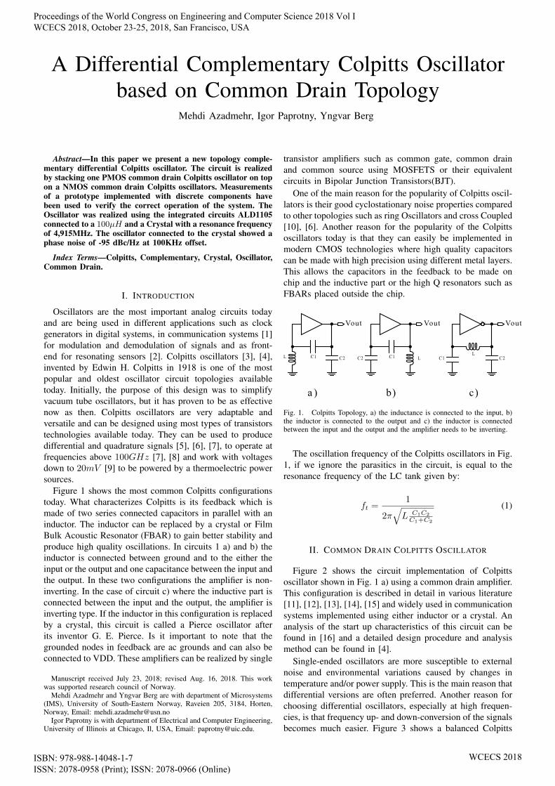
Figure 2 shows the circuit implementation of Colpittsoscillator shown in Fig. 1 a) using a common drain amplifier.This configuration is described in detail in various literature[11], [12], [13], [14], [15] and widely used in communicationsystems implemented using either inductor or a crystal. Ananalysis of the start up characteristics of this circuit can befound in [16] and a detailed design procedure and analysismethod can be found in [4].
Single-ended oscillators are more susceptible to externalnoise and environmental variations caused by changes intemperature and/or power supply. This is the main reason thatdifferential versions are often preferred. Another reason forchoosing differential oscillators, especially at high frequen-cies, is that frequency up- and down-conversion of the signalsbecomes much easier. Figure 3 shows a balanced Colpitts
Proceedings of the World Congress on Engineering and Computer Science 2018 Vol I WCECS 2018, October 23-25, 2018, San Francisco, USA
ISBN: 978-988-14048-1-7 ISSN: 2078-0958 (Print); ISSN: 2078-0966 (Online)
WCECS 2018
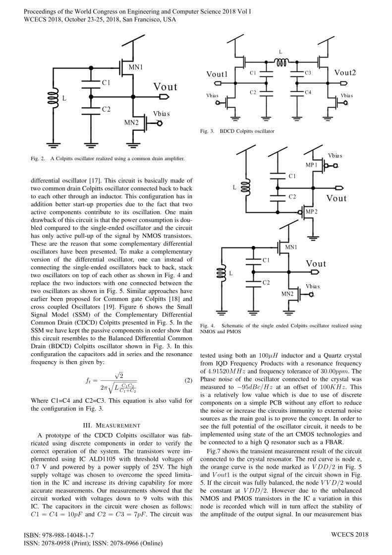
Fig. 2. A Colpitts oscillator realized using a common drain amplifier.
differential oscillator [17]. This circuit is basically made oftwo common drain Colpitts oscillator connected back to backto each other through an inductor. This configuration has inaddition better start-up properties due to the fact that twoactive components contribute to its oscillation. One maindrawback of this circuit is that the power consumption is dou-bled compared to the single-ended oscillator and the circuithas only active pull-up of the signal by NMOS transistors.These are the reason that some complementary differentialoscillators have been presented. To make a complementaryversion of the differential oscillator, one can instead ofconnecting the single-ended oscillators back to back, stacktwo oscillators on top of each other as shown in Fig. 4 andreplace the two inductors with one connected between thetwo oscillators as shown in Fig. 5. Similar approaches haveearlier been proposed for Common gate Colpitts [18] andcross coupled Oscillators [19]. Figure 6 shows the SmallSignal Model (SSM) of the Complementary DifferentialCommon Drain (CDCD) Colpitts presented in Fig. 5. In theSSM we have kept the passive components in order show thatthis circuit resembles to the Balanced Differential CommonDrain (BDCD) Colpitts oscillator shown in Fig. 3. In thisconfiguration the capacitors add in series and the resonancefrequency is then given by:
ft =
√2
2π√L C1C2
C1+C2
(2)
Where C1=C4 and C2=C3. This equation is also valid forthe configuration in Fig. 3.
III. MEASUREMENT
A prototype of the CDCD Colpitts oscillator was fab-ricated using discrete components in order to verify thecorrect operation of the system. The transistors were im-plemented using IC ALD1105 with threshold voltages of0.7 V and powered by a power supply of 25V. The highsupply voltage was chosen to overcome the speed limita-tion in the IC and increase its driving capability for moreaccurate measurements. Our measurements showed that thecircuit worked with voltages down to 9 volts with thisIC. The capacitors in the circuit were chosen as follows:C1 = C4 = 10pF and C2 = C3 = 7pF . The circuit was
Fig. 3. BDCD Colpitts oscillator
Fig. 4. Schematic of the single ended Colpitts oscillator realized usingNMOS and PMOS
tested using both an 100µH inductor and a Quartz crystalfrom IQD Frequency Products with a resonance frequencyof 4.91520MHz and frequency tolerance of 30.00ppm. ThePhase noise of the oscillator connected to the crystal wasmeasured to −95dBc/Hz at an offset of 100KHz. Thisis a relatively low value which is due to use of discretecomponents on a simple PCB without any effort to reducethe noise or increase the circuits immunity to external noisesources as the main goal is to prove the concept. In order tosee the full potential of the oscillator circuit, it needs to beimplemented using state of the art CMOS technologies andbe connected to a high Q resonator such as a FBAR.
Fig.7 shows the transient measurement result of the circuitconnected to the crystal resonator. The red curve is node e,the orange curve is the node marked as V DD/2 in Fig. 5and V out1 is the output signal of the circuit shown in Fig.5. If the circuit was fully balanced, the node V V D/2 wouldbe constant at V DD/2. However due to the unbalancedNMOS and PMOS transistors in the IC a variation in thisnode is recorded which will in turn affect the stability ofthe amplitude of the output signal. In our measurement bias
Proceedings of the World Congress on Engineering and Computer Science 2018 Vol I WCECS 2018, October 23-25, 2018, San Francisco, USA
ISBN: 978-988-14048-1-7 ISSN: 2078-0958 (Print); ISSN: 2078-0966 (Online)
WCECS 2018
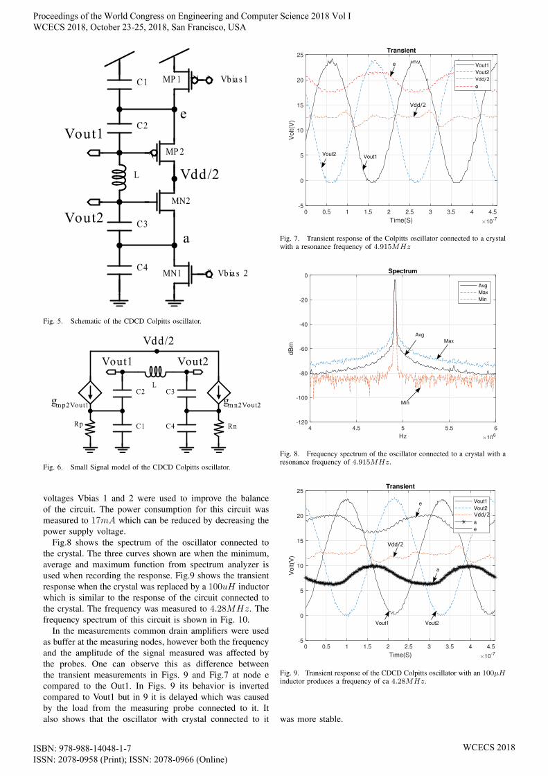
Fig. 5. Schematic of the CDCD Colpitts oscillator.
Fig. 6. Small Signal model of the CDCD Colpitts oscillator.
voltages Vbias 1 and 2 were used to improve the balanceof the circuit. The power consumption for this circuit wasmeasured to 17mA which can be reduced by decreasing thepower supply voltage.
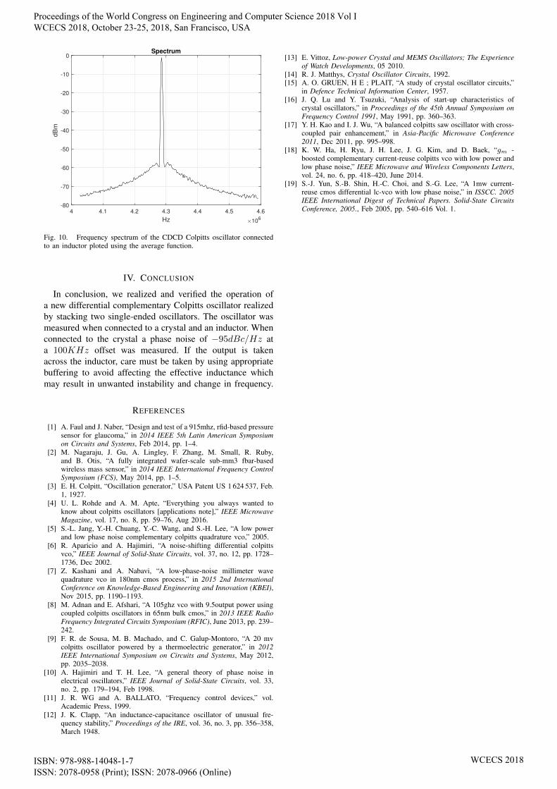
Fig.8 shows the spectrum of the oscillator connected tothe crystal. The three curves shown are when the minimum,average and maximum function from spectrum analyzer isused when recording the response. Fig.9 shows the transientresponse when the crystal was replaced by a 100uH inductorwhich is similar to the response of the circuit connected tothe crystal. The frequency was measured to 4.28MHz. Thefrequency spectrum of this circuit is shown in Fig. 10.
In the measurements common drain amplifiers were usedas buffer at the measuring nodes, however both the frequencyand the amplitude of the signal measured was affected bythe probes. One can observe this as difference betweenthe transient measurements in Figs. 9 and Fig.7 at node ecompared to the Out1. In Figs. 9 its behavior is invertedcompared to Vout1 but in 9 it is delayed which was causedby the load from the measuring probe connected to it. Italso shows that the oscillator with crystal connected to it
Fig. 7. Transient response of the Colpitts oscillator connected to a crystalwith a resonance frequency of 4.915MHz
Fig. 8. Frequency spectrum of the oscillator connected to a crystal with aresonance frequency of 4.915MHz.
Fig. 9. Transient response of the CDCD Colpitts oscillator with an 100µHinductor produces a frequency of ca 4.28MHz.
was more stable.
Proceedings of the World Congress on Engineering and Computer Science 2018 Vol I WCECS 2018, October 23-25, 2018, San Francisco, USA
ISBN: 978-988-14048-1-7 ISSN: 2078-0958 (Print); ISSN: 2078-0966 (Online)
WCECS 2018
4 4.1 4.2 4.3 4.4 4.5 4.6
Hz 106
-80
-70
-60
-50
-40
-30
-20
-10
0dB
mSpectrum
Fig. 10. Frequency spectrum of the CDCD Colpitts oscillator connectedto an inductor ploted using the average function.
IV. CONCLUSION
In conclusion, we realized and verified the operation ofa new differential complementary Colpitts oscillator realizedby stacking two single-ended oscillators. The oscillator wasmeasured when connected to a crystal and an inductor. Whenconnected to the crystal a phase noise of −95dBc/Hz ata 100KHz offset was measured. If the output is takenacross the inductor, care must be taken by using appropriatebuffering to avoid affecting the effective inductance whichmay result in unwanted instability and change in frequency.
REFERENCES
[1] A. Faul and J. Naber, “Design and test of a 915mhz, rfid-based pressuresensor for glaucoma,” in 2014 IEEE 5th Latin American Symposiumon Circuits and Systems, Feb 2014, pp. 1–4.
[2] M. Nagaraju, J. Gu, A. Lingley, F. Zhang, M. Small, R. Ruby,and B. Otis, “A fully integrated wafer-scale sub-mm3 fbar-basedwireless mass sensor,” in 2014 IEEE International Frequency ControlSymposium (FCS), May 2014, pp. 1–5.
[3] E. H. Colpitt, “Oscillation generator,” USA Patent US 1 624 537, Feb.1, 1927.
[4] U. L. Rohde and A. M. Apte, “Everything you always wanted toknow about colpitts oscillators [applications note],” IEEE MicrowaveMagazine, vol. 17, no. 8, pp. 59–76, Aug 2016.
[5] S.-L. Jang, Y.-H. Chuang, Y.-C. Wang, and S.-H. Lee, “A low powerand low phase noise complementary colpitts quadrature vco,” 2005.
[6] R. Aparicio and A. Hajimiri, “A noise-shifting differential colpittsvco,” IEEE Journal of Solid-State Circuits, vol. 37, no. 12, pp. 1728–1736, Dec 2002.
[7] Z. Kashani and A. Nabavi, “A low-phase-noise millimeter wavequadrature vco in 180nm cmos process,” in 2015 2nd InternationalConference on Knowledge-Based Engineering and Innovation (KBEI),Nov 2015, pp. 1190–1193.
[8] M. Adnan and E. Afshari, “A 105ghz vco with 9.5output power usingcoupled colpitts oscillators in 65nm bulk cmos,” in 2013 IEEE RadioFrequency Integrated Circuits Symposium (RFIC), June 2013, pp. 239–242.
[9] F. R. de Sousa, M. B. Machado, and C. Galup-Montoro, “A 20 mvcolpitts oscillator powered by a thermoelectric generator,” in 2012IEEE International Symposium on Circuits and Systems, May 2012,pp. 2035–2038.
[10] A. Hajimiri and T. H. Lee, “A general theory of phase noise inelectrical oscillators,” IEEE Journal of Solid-State Circuits, vol. 33,no. 2, pp. 179–194, Feb 1998.
[11] J. R. WG and A. BALLATO, “Frequency control devices,” vol.Academic Press, 1999.
[12] J. K. Clapp, “An inductance-capacitance oscillator of unusual fre-quency stability,” Proceedings of the IRE, vol. 36, no. 3, pp. 356–358,March 1948.
[13] E. Vittoz, Low-power Crystal and MEMS Oscillators; The Experienceof Watch Developments, 05 2010.
[14] R. J. Matthys, Crystal Oscillator Circuits, 1992.[15] A. O. GRUEN, H E ; PLAIT, “A study of crystal oscillator circuits,”
in Defence Technical Information Center, 1957.[16] J. Q. Lu and Y. Tsuzuki, “Analysis of start-up characteristics of
crystal oscillators,” in Proceedings of the 45th Annual Symposium onFrequency Control 1991, May 1991, pp. 360–363.
[17] Y. H. Kao and I. J. Wu, “A balanced colpitts saw oscillator with cross-coupled pair enhancement,” in Asia-Pacific Microwave Conference2011, Dec 2011, pp. 995–998.
[18] K. W. Ha, H. Ryu, J. H. Lee, J. G. Kim, and D. Baek, “gm -boosted complementary current-reuse colpitts vco with low power andlow phase noise,” IEEE Microwave and Wireless Components Letters,vol. 24, no. 6, pp. 418–420, June 2014.
[19] S.-J. Yun, S.-B. Shin, H.-C. Choi, and S.-G. Lee, “A 1mw current-reuse cmos differential lc-vco with low phase noise,” in ISSCC. 2005IEEE International Digest of Technical Papers. Solid-State CircuitsConference, 2005., Feb 2005, pp. 540–616 Vol. 1.
Proceedings of the World Congress on Engineering and Computer Science 2018 Vol I WCECS 2018, October 23-25, 2018, San Francisco, USA
ISBN: 978-988-14048-1-7 ISSN: 2078-0958 (Print); ISSN: 2078-0966 (Online)
WCECS 2018