A di erential memristive synapse circuit for on-line ... · A di erential memristive synapse...
27
A differential memristive synapse circuit for on-line learning in neuromorphic computing systems Manu V Nair, Lorenz K. Muller, and Giacomo Indiveri Institute of Neuroinformatics, University of Zurich and ETH Zurich E-mail: mnair|lorenz|[email protected] May 2017 Abstract. Spike-based learning with memristive devices in neuromorphic computing architectures typically uses learning circuits that require overlapping pulses from pre- and post-synaptic nodes. This imposes severe constraints on the length of the pulses transmitted in the network, and on the network’s throughput. Furthermore, most of these circuits do not decouple the currents flowing through memristive devices from the one stimulating the target neuron. This can be a problem when using devices with high conductance values, because of the resulting large currents. In this paper we propose a novel circuit that decouples the current produced by the memristive device from the one used to stimulate the post-synaptic neuron, by using a novel differential scheme based on the Gilbert normalizer circuit. We show how this circuit is useful for reducing the effect of variability in the memristive devices, and how it is ideally suited for spike-based learning mechanisms that do not require overlapping pre- and post-synaptic pulses. We demonstrate the features of the proposed synapse circuit with SPICE simulations, and validate its learning properties with high-level behavioral network simulations which use a stochastic gradient descent learning rule in two classification tasks. 1. Introduction Neuromorphic computing systems typically comprise neuron and synapse circuits arranged in a massively parallel manner to support the emulation of large-scale spiking neural networks [3, 10, 21, 23, 28, 31, 36, 42]. In these systems, the bulk of the silicon real-estate is taken up by synaptic circuits, where the memory and computational sites are co-localized [23]. Consequently, to save area and maximize density, many neuromorphic computing approaches avoid implementing complex synaptic circuits with on-chip learning mechanisms [28, 32, 41], and resort to training the network on external computers. However, these approaches lose the ability to execute on- line “life-long” learning and require that the network parameters (such as the synaptic weights) be programmed at deployment time. In addition, if these parameters are stored in Static Random Access Memory (SRAM) cells or in Dynamic Random Access Memory (DRAM) banks, they need to be re-programmed every time the system is arXiv:1709.05484v1 [cs.ET] 16 Sep 2017
Transcript of A di erential memristive synapse circuit for on-line ... · A di erential memristive synapse...
A differential memristive synapse circuit for on-linelearning in neuromorphic computing systems
Manu V Nair, Lorenz K. Muller, and Giacomo IndiveriInstitute of Neuroinformatics, University of Zurich and ETH Zurich
E-mail: mnair|lorenz|[email protected]
May 2017
Abstract. Spike-based learning with memristive devices in neuromorphic computingarchitectures typically uses learning circuits that require overlapping pulses from pre-and post-synaptic nodes. This imposes severe constraints on the length of the pulsestransmitted in the network, and on the network’s throughput. Furthermore, most ofthese circuits do not decouple the currents flowing through memristive devices fromthe one stimulating the target neuron. This can be a problem when using deviceswith high conductance values, because of the resulting large currents. In this paperwe propose a novel circuit that decouples the current produced by the memristivedevice from the one used to stimulate the post-synaptic neuron, by using a noveldifferential scheme based on the Gilbert normalizer circuit. We show how this circuitis useful for reducing the effect of variability in the memristive devices, and how itis ideally suited for spike-based learning mechanisms that do not require overlappingpre- and post-synaptic pulses. We demonstrate the features of the proposed synapsecircuit with SPICE simulations, and validate its learning properties with high-levelbehavioral network simulations which use a stochastic gradient descent learning rulein two classification tasks.
1. Introduction
Neuromorphic computing systems typically comprise neuron and synapse circuitsarranged in a massively parallel manner to support the emulation of large-scale spikingneural networks [3, 10, 21, 23, 28, 31, 36, 42]. In these systems, the bulk of the siliconreal-estate is taken up by synaptic circuits, where the memory and computationalsites are co-localized [23]. Consequently, to save area and maximize density, manyneuromorphic computing approaches avoid implementing complex synaptic circuitswith on-chip learning mechanisms [28, 32, 41], and resort to training the networkon external computers. However, these approaches lose the ability to execute on-line “life-long” learning and require that the network parameters (such as the synapticweights) be programmed at deployment time. In addition, if these parameters arestored in Static Random Access Memory (SRAM) cells or in Dynamic Random AccessMemory (DRAM) banks, they need to be re-programmed every time the system is
arX
iv:1
709.
0548
4v1
[cs
.ET
] 1
6 Se
p 20
17

DiffMemSyn 2
reset. For large networks [15, 28, 44], the time required to initialize the system withthese parameters can become prohibitive.
Memristive devices can potentially address these problems by virtue of theircompactness and non-volatility [22]. Given their advantages, several neuromorphicarrays that use memristive devices have been proposed [25, 30, 39, 40, 48]. Typically,these approaches propose to use memristive devices in dense synaptic arrays forimplementing large-scale neural networks. For instance, [37, 40] describe use of 1Rarrays to implement perceptrons trained by supervised learning protocols such as [45].Similarly, in [50], the authors train a 1T-1R array to implement perceptrons classifyingface images from the Yale face database [17]. In [14], the authors use the RecursiveLeast-Squares (RLS) algorithm for training synaptic weights to perform complex taskssuch as human motor control. In works such as [14, 40], the authors propose the useof two devices per synaptic element to implement positive and negative weight terms.Other approaches describe synaptic arrays with a 1T-1R synapse elements that learnusing classical [11, 16, 39, 43, 48] or stochastic [4, 30, 46] Spike-Timing DependentPlasticity (STDP) learning rules. In these arrays the currents used to program thememristive devices can be very large, especially for devices in high-conductance states.This imposes severe restrictions on the power budget, capacitor sizes, and other aspectsfor the design of ultra-low power memristive-neuromorphic circuits. Moreover, thelearning protocols employed in most of these architectures couple the length of the pulsesused to transmit signals across the layers of the network with the duration of the pulsesrequired to program the devices [16, 39]. This requirement imposes severe constraintson the maximum data throughput of the network, because each row or column in thecross-bar array has to wait for the pre- and post-synaptic pulses to finish, before a newone can be sent. In this paper we propose a novel synaptic circuit that addresses at thesame time both the large current and overlapping pulses problems. To overcome theproblem of integrating large currents in the post-synaptic neuron, we propose a noveldifferential-mode sub-threshold memristive synapse circuit that decouples, normalizes,and re-scales the memristive device current from the one supplied to the post-synapticneuron. To overcome the problem of overlapping pulses in cross-bar architectures, wepropose an event-based scheme that decouples the duration of the input spikes from theread and update phases of the target synapse, coupled with the use of a novel spike-basedsynaptic update mechanism.
In recent years, several algorithms employing spike-triggered learning based onpost-synaptic neuronal activity, instead of vanilla STDP mechanisms, have beenproposed in computational neuroscience literature [6, 20, 49]. Several neuromorphicimplementations of these mechanisms have also been realized [19, 21, 31, 33, 42]. Inthis paper, we demonstrate how the proposed differential memristive synapse circuit canbe incorporated in a neuromorphic system that employs a learning circuit based on suchideas. This circuit is inspired by the biologically plausible learning rule presented in [49]and gradient-descent based methods applied to memristive devices [35, 47]. We usethese learning circuits to implement a randomized unregulated step descent algorithm,

DiffMemSyn 3
AER INPUT
AER
OU
TPU
T
BIASES
Siliconneuron
Memristivesynapse
Pulseshaper
Figure 1: Multi-neuron chip architecture: input AER events are converted into read and writepulses sent to multiple memristive synapses; the currents produced by the synaptic circuits areintegrated by the neuron assigned for the row; ouput spikes are converted into AER events andtransmitted off-chip.
AERPULSE EXTENDER
ReadPULSE EXTENDER
UP
DN
Set
Reset
Write
Figure 2: Pulse-shaping circuit for creating a sequence of Read and Write pulses, with eachAER input event.
which has been shown to be effective for synaptic elements with limited precision [34].In the following Section, we present the network architecture that is compatible
with the proposed differential memristive synapse circuit. In Section 3 we describethe techniques used for sensing and changing the memristive device conductances, andpresent circuit simulation results that quantify its performance figures. In Section 4, weassess the features of neuromorphic architectures that make use of the proposed circuitsand validate them with behavioral simulations in a binary classification task. Finally,in the Supplementary material we present extensions and variants to the proposeddifferential synapse memory cell, including their use in dense 1T-1R cross-bar arrays.
2. Neuromorphic architectures for memristive synapses
The architecture we propose is composed of an array of synapses and neurons thatreceive input spikes into columns of synaptic cells, and produce output spikes from thesilicon neurons arranged in rows (see Fig. 1). This type of architecture can be integratedwithin a full-custom neuromorphic Very Large Scale Integration (VLSI) chip, or be usedas a single-core in multi-core neuromorphic systems [28, 32]. Both the input and outputspikes are represented by fast digital pulses that are encoded using the AER [5, 9, 12,29].
DiffMemSyn 4
DPI+
Iw1+ Iw2+ Iwn+
Iw1- Iw2- Iwn-DPI-
+- LEARNING
V1 V2 Vn
Iwi+
Iwi-
Iteach
I&FNEURON
IoutIin
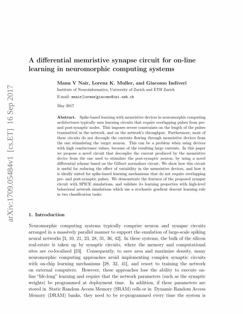
Figure 3: Memristive synapse circuits for on-line learning in a neuromorphic architecture.
On the input side, asynchronous AER circuits ensure that events are transmittedas they arrive. Upon the arrival of a pre-synaptic address-event a pulse-shaping circuitdecouples the duration of the input spikes from the read and update phases of the targetsynapse. This frees the communication bus to transmit spikes from sender nodes to thecross-bar array, increasing the throughput of the network by use of shared or time-multiplexed communication resources. The block diagram describing the operation ofthe pulse-shaping circuits is shown in Fig. 2. The pulse-shaping circuit consists of twopulse-extender circuits [42] and is configured to produce two pulses in quick succession onthe arrival of an AER event. These pulses sequentially enable the read-mode operation,where the state of the addressed synapse is sensed, followed by the write-mode operation,where the state of the memristive devices are increased or decreased, in the targettedsynapse. The write-mode operation is directed by the UP and DN control signalsproduced by the learning circuits in the post-synaptic neuron.
On the output side a 1-D arbiter circuit enqueues output events in case of collisionsand transmits them on the shared output bus [5]. A programmable bias-generatorcircuit [13] provides a set of globally-shared temperature-compensated current signalsfor biasing the analog parameters of the neuromorphic circuits, such as time-constants,refractory periods, or learning rates.
Address-events target destination columns of the memristive array. Byconstruction, all rows of the stimulated column will process the input event in parallel.Furthermore, the extended read and write pulses typically last longer than the inputAER event duration. Therefore, a sequential AER stimulation of multiple columns willproduce multiple read/write operations across the full array that will overlap in time andoperate in parallel. A block diagram of the circuits present in a single row of the cross-bar architecture illustrated in Fig. 1 is shown in Fig. 3. It comprises multiple synapticcircuits that receive the voltage pulses from the pulse-shaping circuits, two current-modeDifferential Pair Integrator (DPI) circuits that emulate excitatory and inhibitory synapsedynamics with biologically realistic time constants [1, 2], a current-mode learning blockthat implements a spike-driven learning mechanism [31, 42], and an ultra-low-poweradaptive Integrate-and-Fire (I&F) neuron circuit that faithfully reproduces biologicallyrealistic neural dynamics [24, 27]. In the read-phase, the synaptic circuit senses the stateof the two memristive devices in it, and produces rescaled and normalized differentialcurrents that are driven into the positive and negative DPI inputs. The DPI circuits

DiffMemSyn 5
integrate these weighted currents and generate a rescaled output current that is driveninto a neuron and its learning block. The learning block uses a copy of this “dendritic”current to compare it to the net input current, which includes contributions from theneuron and an external source. The external source could represent a teacher signalin supervised learning protocols, or contributions from other neurons in unsupervisedlearning protocols. Based on this comparison, the learning block evaluates an error signaland produces the UP and DN weight update control signals that are used during thewrite-mode phase to increase or decrease the weights of the stimulated target synapse.We demonstrate the operation of this architecture with a concrete example in Section 4.
3. The differential memristive synapse circuit
The differential memristive synapse circuit is based on the classic Gilbert-normalizerelement [18, 26], whose output currents, originally designed for bipolar transistors, butfunctional also for Metal Oxide Semiconductor Field-Effect Transistors (MOSFETs)operated in the sub-threshold domain [26]. The synapse circuit stores its weight asthe difference between the conductances of two memristive devices, one representing apositive term and the other representing a negative term. Programming the devicesis done in a push-pull manner: to increase the synaptic weight, the conductanceof the positive term is increased, and that of the negative term is decreased. Thecomplementary operation is achieved by simultaneously decreasing and increasing theconductances of the positive and negative terms, respectively. The output currentproduced by this circuit, in read-mode, can be scaled to very low values (e.g., in therange of pico Amperes). This reduces the total current driven into the post-synapticneuron, which can then be implemented with very small capacitors and ultra-lowpower sub-threshold circuits. The differential operation coupled with the normalizingability of the circuit has two additional advantages. It reduces the effect of memristivedevice variability and implements both positive (excitatory) and negative (inhibitory)synapse contributions, effectively doubling the “high-low” dynamic range of the synapticweight. In write-mode, the circuit enables programming the memristive devices withprogrammable current limits, pulse widths, and heights. These can be chosen by theuser to optimize the write-mode power consumption depending on the memristive deviceintegrated in the circuit.
The operating principles of the circuit is independent of the memristive devicetechnology used. It can be used in combination with a wide range of differentresistive memory technologies, with arbitrary number of resistive stable states. Inthis work we assume our Complementary Metal-Oxide-Semiconductor (CMOS) circuitscan be directly interfaced to HfO2 based devices through post-processing methods, asdescribed in [8].
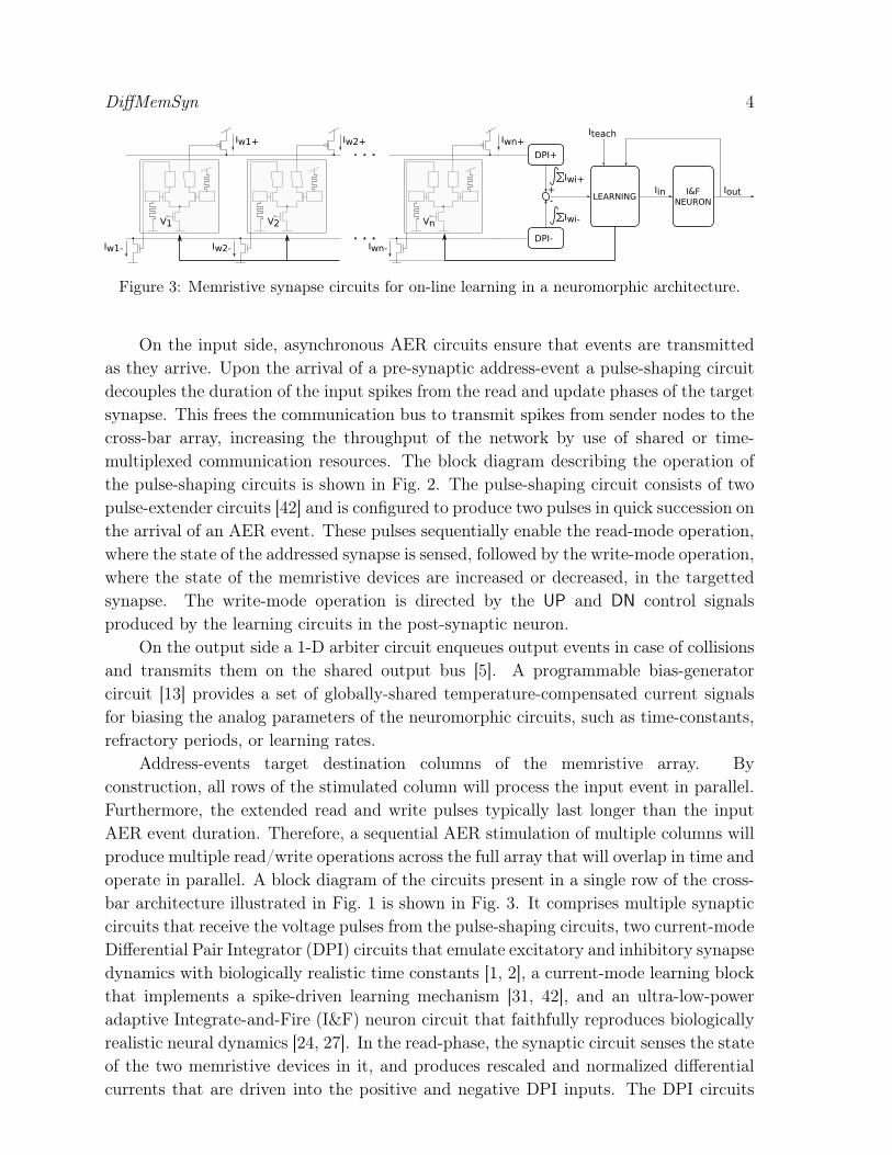
The schematic diagram of the differential memristive synapse circuit is shown inFig. 4. The circuit is used in a “read-mode” phase to measure the conductance ofthe two memristive devices produce scaled output currents that are conveyed to the
DiffMemSyn 6
Ipos Ineg
Vb
VRead
VREAD
M1 M2 M3 M4
M5
S13
V1 V4
VRD
Vtopp
Vbotp
VRD
Vtopn
Vbotn
DposDneg
IbVs Vs
Vc
VST
VREAD
VRESET
VRESET
VSET
Vlim
VST
VSET
VRSTVRST
VREAD
S1
S2S3S6
S4S5 S7
S8 S9
S10
S12
S11
VlimM7 M8
VSET VSET
VREAD
VRESET
VRESET
Figure 4: Differential memristive synaptic circuit.
downstream current-mode neural processing circuits. It is then operated in a “write-mode” for updating the state of the memristive devices via the downstream learningcircuit control signals. All Si MOSFETs represent switches, with gates controlled bydigital signals. Signals with an overline, such as X, represent the inverted version of thesignal X. The signal VRead represents the digital voltage used during the read-mode,while the signals VSet and VReset represent the digital set and reset pulses used in thewrite-mode to increase/decrease the synaptic weight. The signal Vb is a sub-thresholdbias voltage that sets the (sub-threshold) scale of the output currents. The MOSFETsSx have dimensionsW/L = 5µm/0.5µm; MOSFETs M1 & M4 haveW/L = 1µm/2µm,M2 & M3 have W/L = 0.5µm/1µm, and M5 W/L = 2µm/1µm.
3.1. Read-mode operation
To operate the circuit of Fig. 4 in read-mode, the switches S1, S2, S7, and S8 are turnedon and all other switches are turned off; the digital control signals Vset and Vreset areset to logical zero. The current-mode normalizer circuit is implemented by MOSFETsM1-M6. In this mode of operation the memristive devices Dpos and Dneg are connectedto corresponding Vtop and Vbot nodes. When the Vread pulse is active the currents flowingthrough the memristive devices are measured and the output currents, Ipos and Ineg, aresent to the excitatory and inhibitory DPI circuits, respectively.
Therefore, in this mode of operation, during a Vread pulse:
IDpos =IM1 and
IDneg =IM4 (1)

DiffMemSyn 7
where IDx is the current through the device Dx, and IMi is the current through theMOSFET Mi.
For low-power operation, it is desirable to make IDx very small. Under thiscondition, we can assume that the transistors operate in sub-threshold domain. Thisallows us to analytically derive the relationship between the circuit parameters, andthe current flowing through the circuit’s output branches. By writing the sub-thresholdequations for a MOSFET and equating it to the currents through the resistive devices,we get:
(VRD − Vi) =RxIx
IMi =I0eκVi−VsUT (2)
Ix =IMi
where Rx represents the resistance of the memristive device Dx, VRD the supply voltageprovided in “read-mode”, Vs the source voltage of the input MOSFETs M1 and M4, Vithe gate voltage of the MOSFET Mi, κ the sub-threshold slope factor [26], and UT thethermal voltage. By solving for Vi:
Ix = I0e−κRxIxUT e
κVRD−VsUT (3)
If RxIx is sufficiently small, then
I0e−κRxIxUT ≈ I0(1−
κ
UTRxIx) (4)
soIx = IMi = I0
1
e−κVRD−Vs
UT + κUTRxI0
(5)
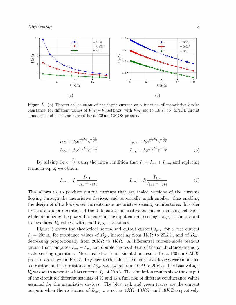
Equation 5 describes how the input current changes with the conductance of thememristive device, and with VRD and Vs voltages. In particular, for large VRD−Vs values,the current is approximately linear with respect to the memristive device conductance,but assumes relatively large values (large values make the circuit less power-efficient).For very small VRD − Vs voltage differences, the circuit produces very small currentsthat change linearly, but with a very small dependence on the device memristance Rx.The effect of this trade-off is highlighted in Fig. 5a, which plots eq. 5 for different valuesof Vs, with VRD set to 1.8V. Figure 5b shows circuit simulations results, carried outusing a standard 130 nm CMOS process, which support the theoretical analysis. VRDwas set to 1.8V, while Vs was swept to obtain the three different VRD−Vs values shownin the figure legend. In this mode of operation the voltage applied across the memristivedevice is set low enough to prevent conductance changes. This allows us to model thedevice as a fixed resistor, and to characterize the circuit as a function of all resistancevalues between the memristive device’s low and high resistance states.
The output currents of the differential memristive circuit are directly proportionalto the input currents sensed from the corresponding input branch and scaled by the biascurrent Ib. Specifically,if all transistors operate in sub-threshold saturation domain:
DiffMemSyn 8
5 10 15R (K Ω)
2
4
6
8
10
I(µ
A)
Vrd - Vs = 0.95 V
Vrd - Vs = 0.925 V
Vrd - Vs = 0.9 V
(a)
0 5 10 15 20R (K Ω)
2.5
3.0
3.5
4.0
I(µ
A)
Vrd - Vs = 0.95 V
Vrd - Vs = 0.925 V
Vrd - Vs = 0.9 V
(b)
Figure 5: (a) Theoretical solution of the input current as a function of memristive deviceresistance, for different values of VRD − Vs settings, with VRD set to 1.8V. (b) SPICE circuitsimulations of the same current for a 130 nm CMOS process.
IM1 = I0eκUT
V1e− VsUT Ipos = I0e
κUT
V1e− VcUT
IM4 = I0eκUT
V4e− VsUT Ineg = I0e
κUT
V4e− VcUT (6)
By solving for e−VcUT using the extra condition that Ib = Ipos + Ineg, and replacing
terms in eq. 6, we obtain:
Ipos = IbIM1
IM1 + IM4
Ineg = IbIM4
IM1 + IM4
(7)
This allows us to produce output currents that are scaled versions of the currentsflowing through the memristive devices, and potentially much smaller, thus enablingthe design of ultra low-power current-mode memristive sensing architectures. In orderto ensure proper operation of the differential memristive output normalizing behavior,while minimizing the power dissipated in the input current sensing stage, it is importantto have large Vs values, with small VRD − Vs values.
Figure 6 shows the theoretical normalized output current Ipos, for a bias currentIb = 20nA, for resistance values of Dpos increasing from 1KΩ to 20KΩ, and of Dneg
decreasing proportionally from 20KΩ to 1KΩ. A differential current-mode readoutcircuit that computes Ipos − Ineg can double the resolution of the conductance/memorystate sensing operation. More realistic circuit simulation results for a 130 nm CMOSprocess are shown in Fig. 7. To generate this plot, the memristive devices were modelledas resistors and the resistance of Dpos was swept from 100Ω to 20KΩ. The bias voltageVb was set to generate a bias current, Ib, of 20 nA. The simulation results show the outputof the circuit for different settings of Vs and as a function of different conductance valuesassumed for the memristive devices. The blue, red, and green traces are the currentoutputs when the resistance of Dneg was set as 1KΩ, 10KΩ, and 19KΩ respectively.

DiffMemSyn 9
5 10 15R (K Ω)
5
10
15
I(n
A)
Vrd - Vs = 0.95 V
Vrd - Vs = 0.925 V
Vrd - Vs = 0.9 V
Figure 6: Theoretical normalized output current of the analytic differential memristive circuitas a function of 20 different memristive conductance values, for three different (VRD − Vs)settings, with Ib = 20nA, and Vrd = 1.8V .
0.0 2.5 5.0 7.5 10.0 12.5 15.0 17.5 20.0
Dpos(K Ω)
4
6
8
10
12
14
16
I(n
A)
Ipos
Ineg
Dneg=1KΩ
Dneg=10KΩ
Dneg=19KΩ
Vrd-Vs=0.95V
Vrd-Vs=0.925V
Vrd-Vs=0.9V
Figure 7: Circuit simulation results for the transfer characteristics of the normalizer circuit.Different colors represent different the circuit response for different values of the Dneg resistor.Solid traces represent the current Ipos while dashed ones represent Ineg. Different markersdenote different Vrd − Vs settings.
The solid and dashed lines plot Ipos and Ineg respectively. It can be seen from the plotsthat the cross over point shifts as the resistance values of Dneg change. Note how thelinearity of the circuit is improved when Vrd − Vs is reduced, at the cost of slightlyreduced difference between Ipos and Ineg.
DiffMemSyn 10
2 4 6 8 10Resistance (kΩ)
0.0
0.2
0.4
0.6
0.8ΩDpos
ΩDneg
(a)
0 5 10 15 20I(n A)
0.00
0.05
0.10
0.15
0.20
0.25Ipos
Ineg
(b)
0 2 4 6 8Ωpos − Ωneg(kΩ)
−5
0
5
10
15
20
I pos−I neg
(nA
)
(c)
0 100 200 300 400Resistance high-low ratio
0.0
0.2
0.4
0.6
0.8
CV
Ωpos − Ωneg
Ipos − Ineg
(d)
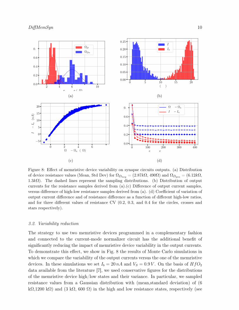
Figure 8: Effect of memristive device variability on synapse circuits outputs. (a) Distributionof device resistance values (Mean, Std Dev) for ΩDneg = (2.87kΩ, 490Ω) and ΩDpos = (6.12kΩ,1.3kΩ). The dashed lines represent the sampling distributions. (b) Distribution of outputcurrents for the resistance samples derived from (a).(c) Difference of output current samples,versus difference of high-low resistance samples derived from (a). (d) Coefficient of variation ofoutput current difference and of resistance difference as a function of different high-low ratios,and for three different values of resistance CV (0.2, 0.3, and 0.4 for the circles, crosses andstars respectively).
3.2. Variability reduction
The strategy to use two memristive devices programmed in a complementary fashionand connected to the current-mode normalizer circuit has the additional benefit ofsignificantly reducing the impact of memristive device variability in the output currents.To demonstrate this effect, we show in Fig. 8 the results of Monte Carlo simulations inwhich we compare the variability of the output currents versus the one of the memristivedevices. In these simulations we set Ib = 20nA and VS = 0.9V . On the basis of HfO2
data available from the literature [7], we used conservative figures for the distributionsof the memristive device high/low states and their variance. In particular, we sampledresistance values from a Gaussian distribution with (mean,standard deviation) of (6kΩ,1200 kΩ) and (3 kΩ, 600 Ω) in the high and low resistance states, respectively (see

DiffMemSyn 11
samples in Fig. 8a), and measured the circuit response using such values (see Fig. 8b).We observed that the histogram of the output currents Ipos and Ineg are symmetric,illustrating the effect of normalization, with a standard deviation of approximately2.12nA for both branches. The normalization circuit effectively compresses the errorin output current for large difference between resistances and expands it for smalldifferences as shown in Fig. 8c. Even for these conservative values of resistance figures,with a very small high-low ratio, the reduction in the Coefficient of Variation (CV) wentfrom 0.429 for the Ωpos−Ωneg to 0.284 for Ipos−Ineg. For more typical cases, for examplewith high-low resistance values equivalent to 100KΩ and 10KΩ, the same analysisshows a drastic reduction of CV from 0.219 to 0.003. In Fig. 8 we show a systematiccomparison of the CVs between the basic resistance differences and the output currentdifferences, for increasing ratios of high-low states. The comparison was performedrunning Monte Carlo simulations in which the device high and low resistance stateswere sampled from a normal distribution with three different coefficients of variation(0.2, 0.3, and 0.4), and the output currents were calculated using the circuit’s transferfunction derived analytically in Section 3.
3.3. Write-mode operation
The write-mode operation takes place immediately after the read-mode phase, asdetermined by the sequence of Vread and Vwrite pulses generated by the pulse-shapercircuit of Fig. 2. In this phase, Vread is zero, the Vwrite is high. Furthermore, the switchesof two memristive devices (S4-S10) are turned on in a complementary way, such thatthe resultant voltage across the memristive devices induce opposite changes in theirconductance values. For example, to increase the net output current (Ipos − Ineg), theconductance of Dpos is increased and that of Dneg is decreased. This is done by enablingthe switches S5, S6, S9, and S10 by programming theVset signal to logical one, and Vresetto logical zero. This connects Vtopp to VST , Vbotp to ground, Vbotn to VRST , and Vtopn toground. Similarly, to decrease (Ipos−Ineg), the Vreset signal is to set logical one, and Vsetis set to logical zero. The MOSFETs M7 and M8 are current-limiting transistors thatprotect the devices from damage during programming. The signal Vlim is a bias voltagechosen that ensure that the memristive devices are not damaged during the formingoperation. To minimize power consumption all switching transistors are turned on onlyduring a read or write pulse.
The pulse shaping circuit of Fig 2 can be tuned to increase or decrease thewrite pulse duration. So by programming the length of these pulses and by choosingappropriate values for VST and VRST voltages, it is possible to use this circuit to producereliable binary, gradual, or stochastic changes in the memristive devices [7, 22]. Themode of operation of the memristive devices and the nature of the changes that should beinduced in the memristive device conductance depend on the specific learning algorithmimplemented in the learning block of Fig. 3.

DiffMemSyn 12
4. Learning simulations
In this section we demonstrate examples of spike-based learning simulations using alearning rule that is ideally suited for implementation in neuromorphic architecturesthat comprise the memristive synapse proposed. In the first subsection we learn a singlelow-dimensional pattern with varying contrast, in the second subsection we learn manyoverlapping high-dimensional patterns.
4.1. Single pattern binary classification
Here we show simulation results of two neurons trained to classify an input spike-trainby adjusting their synaptic weights. We study the performance of such a learningsystem connected by multiple binary synapses and compare it to that of a hypothetical32-bit floating-point precision synapse in the same setting. This illustrates what theperformance limitation is with an ‘ideal’ synaptic element for classifying a finite-ratePoisson train with a leaky integrator neuron.
In this task, the neurons a and b are connected via randomly initialized synapsesto two neural populations p1 and p2, which fire with two different average firing rates,with Poissonian statistics. The goal is for neuron a to learn to fire more than neuronb, whenever input units from population p1 fire at a higher rate than input units in p2.To achieve this, we use a supervised training protocol: given the input, we provide ateacher signal to the neuron that should fire more. The teacher signal is representedby a Poissonian spike train sent to the target neurons via an additional, separate,channel. The spike-based learning algorithm is a discretized version of the one presentedin [49]. It performs a gradient descent procedure on the difference of the observed anddesired neuron firing rates, and it can be readily implemented in mixed signal CMOSneuromorphic hardware [34, 42]. A detailed description of this learning rule and theparameter values used are provided in the Supplementary Material.
In Fig. 9 we compare the classifications results produced by the best system using a32-bit floating-point precision synapse with the results obtained simulating the proposedbinary synapse in the same setting. Each of the two variables is proportional to thefiring rate of the respective subpopulation. When they are equal the pattern has no‘constrast’, when they are very different it is strongly contrasted. The colors indicatewhich of the two learning neurons fired more strongly; the ideal solution is a separationof red and blue at a 45 angle. The proposed learning rule finds a good solution tothe classification problem, in that the misclassified points only elicit a slightly higherresponse in the wrong output neuron.
4.2. Classifying multiple patterns
Here we show how it is possible to train a population of output neurons to classifymultiple overlapping patterns in a supervised setting. For this demonstration we usethe common benchmark of classifying handwritten digits from the MNIST data-set.

DiffMemSyn 13
−0.2 0.0 0.2 0.4 0.6 0.8 1.0 1.2Variable 1
−0.2
0.0
0.2
0.4
0.6
0.8
1.0
1.2
Vari
able
2
Best High Resolution
−0.2 0.0 0.2 0.4 0.6 0.8 1.0 1.2Variable 1
−0.2
0.0
0.2
0.4
0.6
0.8
1.0
1.2
Vari
able
2
Best Binary
Figure 9: Comparison of the classification output of the two neuron system with 40 binaryweight elements (left) and 40 floating-point resolution synapses (right). The size of the circlesindicates the difference in output rates of the two neurons.
Namely we test the system using MNIST digits from 0 to 4 scaled to 24 × 24 pixels,as in [4]. In the network, there is an input layer consisting of 24 · 24 · nc Poissonneurons, whose spike rates are scaled according to the intensity of the MNIST digitimage pixel, and the output layer consisting of 5 neurons that should learn to respondto the corresponding digit, and an additional layer of teacher neurons indicating whichof 5 output neurons should fire in response to a given input. The index of the outputneuron that fires the most in response to a test stimulus is considered the label that thenetwork assigns to this input. During training 1000 digits, randomly drawn from thetraining set, are presented for 100ms each while the learning circuits are enabled. Thelearning circuits are then disabled and the performance of the network is evaluated on500 further digits (randomly drawn from the test set). Further implementation detailsare given in the supplementary material.
The learning algorithm is the same one used in Section 4.1. To compensate forthe discretization errors, the update is made probabilistic as in [34]. Although werestrict ourselves to probabilistic signals that are independent per neuron, rather thanper synapse, we achieve a performance comparable to that of [4].
In Fig. 10a we report the performance of the network as a function of the numbernc of synapses used per pixel, in terms of classification accuracy. In Fig. 10b we showtwo examples of the learned weight matrices.

DiffMemSyn 14
1 2 4 8Num. Synapses
0
5
10
15
20
25
30
35
40E
rror
High Variation
Low Variation
(a) Error on the (reduced) MNIST classifica-tion task (test set) as a function of the numberof binary synapses per input pixel for high andlow CV. The CV settings correspond to Fig. 8.Errorbars indicate std. dev. on 5 repetitions.
(b) Learned weight matrices with one andeight synaptic weights.
5. Discussion
The memristive synapse circuit proposed in this paper comprises two memristive devices,20 MOSFETss, and a pulse controller module. Clearly, the resulting synaptic circuitis much larger in area than synapse elements employed in dense 1R or 1T-1R crossbararrays [16, 38, 40]. However, the large area overhead used allows the system to operatemultiple synapses in parallel, both along the rows and along the columns of the synapticarray (e.g., by sending multiple AER pulses in quick succession across multiple columns).In addition, as the currents passing through the memristive devices are contained ineach individual synapse element and do not diffuse to neighboring devices, there areno sneak-path issues and no problems for quickly charging/discharging high capacitiveloads. The strategy of using two memristive devices per synapse allows the use of anormalizer circuit, which has the desirable property of minimizing the effect of variabilityacross the memristive devices. In addition, the strategy adopted to use the two devicesin a differential way, increasing one while decreasing the other, eliminates the needfor a precise reference for the normalizer operations, and provides automatically thepossibility to implement both positive and negative synaptic weights in the network.
6. Conclusion
We proposed a differential current-mode memristive synapse circuit that decouplesthe current used to sense or change memristive device state from the current usedto stimulate ultra low-power post-synaptic neuron circuits. We showed that the circuitproposed significantly reduces the effect of device variability, and that it is ideally suitedfor implementing advanced spike-based learning mechanisms that do not use overlappingpulses at the terminals of the target synapse. We argued that the strategy of usingpulse extenders and Gilbert-normalizers in each synapse element maximizes throughput

REFERENCES 15
and minimizes power consumption in large-scale event-based neuromorphic computingplatforms. For applications that do no require online adpatation or simultaneous read-write functionality, we describe how the synaptic circuit can be integrated with densememristive crossbar arrays (Supplementary material). Given that memory-relatedconstraints, such as size and throughput, represent one of the major bottlenecks inconventional computing architectures [23], and given the potential of neuromorphiccomputing platforms to perform robust computation using variable and slow computingelements, the proposed circuit offers an attractive solution for building alternative nonvon Neumann computing platforms with advanced and emerging memory technologies.
7. Acknowledgements
This work was supported by SNSF grant number CRSII2_160756 and by the EU ICTgrant “NeuRAM3” (687299).
References
[1] C. Bartolozzi and G. Indiveri. “Synaptic dynamics in analog VLSI”. In: NeuralComputation 19.10 (Oct. 2007), pp. 2581–2603.
[2] C. Bartolozzi, S. Mitra, and G. Indiveri. “An ultra low power current–mode filter forneuromorphic systems and biomedical signal processing”. In: Biomedical Circuits andSystems Conference, (BioCAS), 2006. IEEE. 2006, pp. 130–133.
[3] Ben Varkey Benjamin et al. “Neurogrid: A Mixed-Analog-Digital Multichip System forLarge-Scale Neural Simulations”. In: Proceedings of the IEEE 102.5 (2014), pp. 699–716.
[4] J. Bill and R. Legenstein. “A compound memristive synapse model for statistical learningthrough STDP in spiking neural networks”. In: Frontiers in neuroscience 8 (2014).
[5] K.A. Boahen. “Point-to-Point Connectivity Between Neuromorphic Chips UsingAddress-Events”. In: IEEE Transactions on Circuits and Systems II 47.5 (2000), pp. 416–34.
[6] J. Brader, W. Senn, and S. Fusi. “Learning real world stimuli in a neural network withspike-driven synaptic dynamics”. In: Neural Computation 19 (2007), pp. 2881–2912.
[7] S Brivio et al. “Experimental study of gradual/abrupt dynamics of HfO2-basedmemristive devices”. In: Applied Physics Letters 109.13 (2016), p. 133504.
[8] Hong-Yu Chen et al. “Resistive random access memory (RRAM) technology: Frommaterial, device, selector, 3D integration to bottom-up fabrication”. In: Journal ofElectroceramics (June 2017). issn: 1573-8663.
[9] E. Chicca et al. “A multi-chip pulse-based neuromorphic infrastructure and itsapplication to a model of orientation selectivity”. In: IEEE Transactions on Circuitsand Systems I 5.54 (2007), pp. 981–993.
[10] E. Chicca et al. “Neuromorphic electronic circuits for building autonomous cognitivesystems”. In: Proceedings of the IEEE 102.9 (Sept. 2014), pp. 1367–1388. issn: 0018-9219.
[11] Erika Covi et al. “Analog memristive synapse in spiking networks implementingunsupervised learning”. In: Frontiers in neuroscience 10 (2016).

REFERENCES 16
[12] S.R. Deiss, R.J. Douglas, and A.M. Whatley. “A Pulse-Coded CommunicationsInfrastructure for Neuromorphic Systems”. In: Pulsed Neural Networks. Ed. by W. Maassand C.M. Bishop. MIT Press, 1998. Chap. 6, pp. 157–78.
[13] T. Delbruck et al. “32-bit Configurable bias current generator with sub-off-currentcapability”. In: International Symposium on Circuits and Systems, (ISCAS), 2010. IEEE.Paris, France: IEEE, 2010, pp. 1647–1650.
[14] Lei Deng et al. “Complex Learning in Bio-plausible Memristive Networks”. In: Scientificreports 5 (2015).
[15] S.B. Furber et al. “The SpiNNaker Project”. In: Proceedings of the IEEE 102.5 (May2014), pp. 652–665. issn: 0018-9219.
[16] Daniele Garbin et al. “HfO 2-based OxRAM devices as synapses for convolutional neuralnetworks”. In: IEEE Transactions on Electron Devices 62.8 (2015), pp. 2494–2501.
[17] A Georghiades, PN Belhumeur, and DJ Kriegman. “Yale face database”. In:Center for computational Vision and Control at Yale University, http://cvc. yale.edu/projects/yalefaces/yalefa 2 (1997).
[18] B. Gilbert. “Current-Mode Circuits from a Translinear Viewpoint: A Tutorial”. In:Analogue IC design: the current-mode approach. Ed. by C. Tomazou, F.J. Lidgey, andD.G. Haigh. Stevenage, Herts., UK: Peregrinus, 1990. Chap. 2, pp. 11–91.
[19] M. Giulioni et al. “Robust working memory in an asynchronously spiking neural networkrealized in neuromorphic VLSI”. In: Frontiers in Neuroscience 5.149 (2012). issn: 1662-453X.
[20] M. Graupner and N. Brunel. “Calcium-based plasticity model explains sensitivity ofsynaptic changes to spike pattern, rate, and dendritic location”. In: Proceedings of theNational Academy of Sciences 109 (2012), pp. 3991–3996.
[21] Frank L Maldonado Huayaney, Stephen Nease, and Elisabetta Chicca. “Learning inSilicon Beyond STDP: A Neuromorphic Implementation of Multi-Factor SynapticPlasticity With Calcium-Based Dynamics”. In: IEEE Transactions on Circuits andSystems I: Regular Papers 63.12 (2016), pp. 2189–2199.
[22] Daniele Ielmini and Rainer Waser. Resistive Switching: From Fundamentals of NanoionicRedox Processes to Memristive Device Applications. John Wiley & Sons, 2015.
[23] G. Indiveri and S.-C. Liu. “Memory and information processing in neuromorphicsystems”. In: Proceedings of the IEEE 103.8 (2015), pp. 1379–1397.
[24] G. Indiveri et al. “Neuromorphic silicon neuron circuits”. In: Frontiers in Neuroscience5 (2011), pp. 1–23. issn: 1662-453X.
[25] Sung Hyun Jo et al. “Nanoscale memristor device as synapse in neuromorphic systems”.In: Nano letters 10.4 (2010), pp. 1297–1301.
[26] S.-C. Liu et al. Analog VLSI:Circuits and Principles. MIT Press, 2002.[27] P. Livi and G. Indiveri. “A current-mode conductance-based silicon neuron for Address-
Event neuromorphic systems”. In: International Symposium on Circuits and Systems,(ISCAS), 2009. IEEE. May 2009, pp. 2898–2901.
[28] Paul A. Merolla et al. “A million spiking-neuron integrated circuit with a scalablecommunication network and interface”. In: Science 345.6197 (Aug. 2014), pp. 668–673.issn: 0036-8075, 1095-9203.
[29] P.A. Merolla et al. “Expandable Networks for Neuromorphic Chips”. In: IEEETransactions on Circuits and Systems I 54.2 (Feb. 2007), pp. 301–311.
REFERENCES 17
[30] V Milo et al. “Demonstration of hybrid CMOS/RRAM neural networks with spiketime/rate-dependent plasticity”. In: Electron Devices Meeting (IEDM), 2016 IEEEInternational. IEEE. 2016, pp. 16–8.
[31] S. Mitra, S. Fusi, and G. Indiveri. “Real-time classification of complex patterns usingspike-based learning in neuromorphic VLSI”. In: Biomedical Circuits and Systems, IEEETransactions on 3.1 (Feb. 2009), pp. 32–42.
[32] S. Moradi et al. Networks and hierarchical routing fabrics with heterogeneous memorystructures for scalable event-driven computing systems. European patent application EP15/165272. Filed 27.04.2015. Apr. 2015.
[33] Hesham Mostafa, Christian Mayr, and Giacomo Indiveri. “Beyond spike-timingdependent plasticity in memristor crossbar arrays”. In: Circuits and Systems (ISCAS),2016 IEEE International Symposium on. IEEE. 2016, pp. 926–929.
[34] L. Müller, M. Nair, and G. Indiveri. “Randomized Unregulated Step Descent for LimitedPrecision Synaptic Elements”. In: International Symposium on Circuits and Systems,(ISCAS), 2017. submitted. IEEE. 2017.
[35] Manu V Nair and Piotr Dudek. “Gradient-descent-based learning in memristive crossbararrays”. In: Neural Networks (IJCNN), 2015 International Joint Conference on. IEEE.2015, pp. 1–7.
[36] Jongkil Park et al. “A 65k-neuron 73-Mevents/s 22-pJ/event asynchronous micro-pipelined integrate-and-fire array transceiver”. In: Biomedical Circuits and SystemsConference (BioCAS), 2014 IEEE. IEEE. 2014, pp. 675–678.
[37] Sangsu Park et al. “Electronic system with memristive synapses for pattern recognition”.In: Scientific reports 5 (2015), p. 10123.
[38] S Park et al. “RRAM-based synapse for neuromorphic system with pattern recognitionfunction”. In: Electron Devices Meeting (IEDM), 2012 IEEE International. IEEE. 2012,pp. 10–2.
[39] G Pedretti et al. “Memristive neural network for on-line learning and tracking withbrain-inspired spike timing dependent plasticity”. In: Scientific Reports 7 (2017).
[40] Mirko Prezioso et al. “Training and operation of an integrated neuromorphic networkbased on metal-oxide memristors”. In: Nature 521.7550 (2015), pp. 61–64.
[41] N. Qiao and G. Indiveri. “Scaling mixed-signal neuromorphic processors to 28nm FD-SOItechnologies”. In: Biomedical Circuits and Systems Conference, (BioCAS), 2016. IEEE.2016, pp. 552–555.
[42] Ning Qiao et al. “A Re-configurable On-line Learning Spiking Neuromorphic Processorcomprising 256 neurons and 128K synapses”. In: Frontiers in Neuroscience 9.141 (2015).issn: 1662-453X.
[43] S. Saighi et al. “Plasticity in memristive devices”. In: Frontiers in Neuroscience 9.51(2015).
[44] J. Schemmel et al. “A wafer-scale neuromorphic hardware system for large-scale neuralmodeling”. In: Circuits and Systems (ISCAS), Proceedings of 2010 IEEE InternationalSymposium on. IEEE. 2010, pp. 1947–1950.
[45] W Schiffmann, M Joost, and R Werner. “Optimization of the backpropagation algorithmfor training multilayer perceptrons”. In: University of Koblenz: Institute of Physics(1994).

REFERENCES 18
[46] Alexander Serb et al. “Unsupervised learning in probabilistic neural networks with multi-state metal-oxide memristive synapses”. In: Nature communications 7 (2016), p. 12611.
[47] Daniel Soudry et al. “Memristor-based multilayer neural networks with online gradientdescent training”. In: IEEE transactions on neural networks and learning systems 26.10(2015), pp. 2408–2421.
[48] Manan Suri et al. “Phase change memory as synapse for ultra-dense neuromorphicsystems: Application to complex visual pattern extraction”. In: Electron Devices Meeting(IEDM), 2011 IEEE International. IEEE. 2011, pp. 4–4.
[49] Robert Urbanczik and Walter Senn. “Learning by the dendritic prediction of somaticspiking”. In: Neuron 81.3 (2014), pp. 521–528.
[50] Peng Yao et al. “Face classification using electronic synapses”. In: Nature Communica-tions 8 (2017).
Supplementary material:A differential memristive synapse circuit for on-linelearning in neuromorphic computing systems
Manu V Nair, Lorenz K. Muller, and Giacomo IndiveriInstitute of Neuroinformatics, University of Zurich and ETH Zurich
E-mail: mnair|lorenz|[email protected]
1. Learning Simulation Setup
The following differential equations define our neuron model. They were derived in [1]to describe the behavior of a neuron circuit that approximates an exponential adaptiveintegrate-and-fire neuron. Compared to [1] we added an additional term Icomp thatreflects the compensation current injected by the learning circuit, which was not presentin the original equations. This current enforces that the neuron fires in accordance withits input teacher signal.
dIm(t)
dt=Ipos(t)− Im(t) (1 + Iadapt(t)/Iτ )
τm(1 + IthIm(t)+I0
)(1)
dIadapt(t)
dt=Ip − Iadapt(t)
τadapt(2)
Im(t)← Ireset if Im(t) > Ispkthr (3)
With synaptic differential equation
Isyn(t)
dt= −Isyn(t) + Iwwsyn
∑
i
δ(tspikei − t). (4)
For compactness we introduced
Ipos(t) = Ifb(t) +IthIτ
(Iin(t) + Icomp(t) + ISyn(t)− Iadapt(t)− Iτ ) (5)
Ifb(t) =Ia(t)
Iτ(Im(t) + Ith) (6)
Ia(t) =Ig
1 + exp (−(Im(t)− Iath)/Ianorm)(7)
The table 1 clarifies the meanings and where appropriate the values of the abovevariables and parameters.
arX
iv:1
709.
0548
4v1
[cs
.ET
] 1
6 Se
p 20
17

Supplementary Material 2
Name Description ValueIm(t) Membrane Current VariableIpos(t) Positive input to the neuron VariableIadapt(t) Adaptation feedback VariableIτ Neuron time constant bias 2 pAτm Neuron time constant 8.9 msIth Global synaptic input scaling factor 1 pAI0 Leak Current (process parameter) 0.5 pAIp Feedback rate 0.5 pAτadapt Adaptation time constant 17.7 msIreset Membrane reset level 1 pAIspkthr Spike threshold 60 pAIsyn Synaptic input current Variablenin no. synapses per input channel given in plotsIw Synaptic bias current 16 pA (MNIST)Iw Synaptic bias current 1 nA /nin (single pattern)wsyn Synaptic Weight Drawn from distributions
given for device variabilitytspikei Times of presynaptic spikes VariableIfb(t) Feedback current VariableIa(t) Fitting variable for feedback VariableIg Feedback gain 1 nAIath Fitting variable 20 nAIanorm Fitting variable 1 nA
Table 1: Neuron and Synapse Variables and parameters.
1.1. Learning Equations
The learning block acts according to:
dT (t)
dt=−T (t)
τlearn(8)
dS(t)
dt=−S(t)
τlearn(9)
Icomp(t) = gcomp(T (t)− S(t))(t < tstop) (10)
q(t) = (S(t) + S0 − Isyn(t)) (11)
L(t) = sign(q(t)(|q(t)| > α))bp(t) (12)
When a presynaptic spike arrives, wsyn is updated according to the value of L(t).The update is to redraw wsyn from one of the two distributions given in the main paperfor high and low coefficient of variation, rescaled so that both have the same mean. Forthe single pattern simulations the distributions were normal distributions with the same

Supplementary Material 3
Name Description ValueT (t) Teacher signal Variableτlearn learning time constant 8 msS(t) Instantaneous firing rate VariableIcomp Compensation current from learning block Variablegcomp Compensation gain 1.0tstop Time at which teaching input ends nsamp · τsamp
q(t) Cost function VariableS0 Output bias (−500, 0) pA (MNIST, single pattern)L(t) Learning circuit output Variableα Slack variable (300, 500) pA (MNIST, single pattern)bp(t) Bernoulli learning variable p = (0.01, 0.001) (MNIST, single pattern)wS Output spike weight 200 pAwT Teacher spike weight 40 pA
Table 2: Learning circuit variables and parameters.
mean and variance as the aformentioned. Overall this results in a probabilistic binaryupdate.
In the case of the high resolution synapse the last equation becomes an analogupdate proportional to q(t) (with scaling factor 0.0001).
On a postsynaptic spike / a teacher spike wS / wT are instantaneously added toS(t) / T (t).
This implements an update that is similar to [6]; the key differences are the use ofa sign function to limit the output of the circuit to −1, 0, 1 (decrease, keep, increasesynaptic value) and the addition of bp(t) that probabilistically enables / disables thelearning block to implement a form of RUSD [3].
The functional effect of these equations is to perform a gradient descent procedureof brining the output spike rate of the neuron close to the teacher signal (as shown in[6]), but in contrast to [6] updates are discretized and probabilistic as in RUSD [3].
The table 2 clarifies the meanings and where appropriate the values of the abovevariables and parameters.
1.2. Population Level Parameters
The table Tab. 3 gives an overview of the values population level parameters were setto.
2. Advantages of the normalizer circuit over a current mirror
Isolating the current flowing through the device from that sent into the post-synapticneuron can also be achieved by use of a simple current mirror circuit as shown in Fig. 1.

Supplementary Material 4
Description ValueFiring rate positive single pattern (x·50 kHz+5 kHz)/nin; x ∼ U(0.5, 1)
Firing rate negative single pattern (x·50 kHz+5 kHz)/nin; x ∼ U(0, 0.5)
Teacher rate positive single pattern 50 kHzTeacher rate negative single pattern 0 kHzFiring rate MNIST z·100 Hz; z is the pixel valueTeacher rate positive MNIST class 100 HzTeacher rate negative MNIST class 0 HzNo. teacher neurons 40
Table 3: Population level parameters.
This circuit is put in read mode when Read and Read are set to logical 1 and 0 values,respectively. However, with this circuit the Width
Lengthratio between the transistors M1 and
Ix
VRD
Vtop
Vbot
Dx
VlimV M1 M2
VS
RST
VST
VSET
VSET VRESET
VRESET
VREAD
VREAD
Figure 1: A current mirror synaptic memory cell with read and write functionality
M2 will have to be made very large to reduce the output current Ix. For example, toreduce the read current from 1µA to 1nA, which is a typical value for input currentsto sub-threshold silicon neurons [2], would require a ratio of 1000. Secondly, withoutuse of power-hungry active feedback circuit, the drain voltages of M1 and M2 will bedifferent, which will result in poor current mirroring accuracy. The normalizer circuitwe propose addresses both of these issues. The proposed circuit is also more compact.This is because while the normalizer uses two extra transistors (M5 and S13 in Fig. 3),these are the sized comparably to M1-M4. The absence of large scaling factors makesthe total area of the circuit smaller. Note that while the differential synapse circuitcomprises two copies of the basic current mirror, it also provides twice the dynamicrange. Finally, the proposed design can be extended in various ways as described in thefollowing sections.
Supplementary Material 5
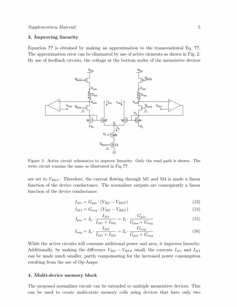
3. Improving linearity
Equation ?? is obtained by making an approximation to the transcendental Eq. ??.The approximation error can be eliminated by use of active elements as shown in Fig. 2.By use of feedback circuits, the voltage at the bottom nodes of the memristive devices
Ipos Ineg
Vb
M1 M2 M3 M4
M5
1 V4
Vtopp
Vbotp
Vtopn
Vbotn
Dpos Dneg
IbVs Vs
Vc
−
+
VREF−
+
VREF
VRD VRD
S13
VREAD
VREAD
VREAD
VREAD
VREAD
Figure 2: Active circuit schematics to improve linearity. Only the read path is shown. Thewrite circuit remains the same as illustrated in Fig ??.
are set to VREF . Therefore, the current flowing through M1 and M4 is made a linearfunction of the device conductance. The normalizer outputs are consequently a linearfunction of the device conductance.
IM1 = Gpos · (VRD − VREF ) (13)
IM4 = Gneg · (VRD − VREF ) (14)
Ipos = Ib ·IM1
IM1 + IM4
= Ib ·Gpos
Gpos +Gneg
(15)
Ineg = Ib ·IM4
IM1 + IM4
= Ib ·Gneg
Gpos +Gneg
(16)
While the active circuits will consume additional power and area, it improves linearity.Additionally, by making the difference VRD − VREF small, the currents IM1 and IM4
can be made much smaller, partly compensating for the increased power consumptionresulting from the use of Op-Amps.
4. Multi-device memory block
The proposed normalizer circuit can be extended to multiple memristive devices. Thiscan be used to create multi-state memory cells using devices that have only two
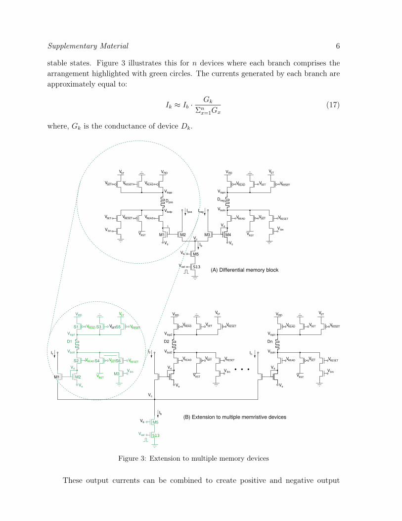
Supplementary Material 6
stable states. Figure 3 illustrates this for n devices where each branch comprises thearrangement highlighted with green circles. The currents generated by each branch areapproximately equal to:
Ik ≈ Ib ·Gk
Σnx=1Gx
(17)
where, Gk is the conductance of device Dk.
In
Vb
Vsel
M5
V4
VRD
Vtopn
Vbotn
Dn
Ib
Vs
Vc
Vlim
I2
V4
VRD
Vtop2
Vbot2
D2
Vs
Vlim
I1
M1 M2
V4
VRD
Vtop1
Vbot1
D1
Vs
S2
S1 S3
S4
S5
S6
VlimM3
Ipos Ineg
Vb
Vsel
M1 M2 M3 M4
M5
1 V4
VRD
Vtopp
Vbotp
VRD
Vtopn
Vbotn
DposDneg
IbVs Vs
Vc
Vlim
(A) Differential memory block
(B) Extension to multiple memristive devices
S13
S13
VlimVRST
VST
VSET
VSET VRESET
VRESET
VREAD
VREAD
VREAD
VREAD
VSET VRESET
VSET VRESET
VREAD
VREAD
VSET VRESET
VSET VRESET
VST
VRST
VST
VRST
VREAD
VREAD
VSET VRESET
VSET VRESET
VST
VRST
VREAD
VREAD
VSET VRESET
VSET VRESET
VST
VRST
Figure 3: Extension to multiple memory devices
These output currents can be combined to create positive and negative output

Supplementary Material 7
currents in different ways, depending on the application. For example,
Ipos =m−1∑
x=1
Ix (18)
Ineg =n∑
x=m
Ix (19)
Another possibility to expand the dynamic range of the output currents is to weighthe currents output from each branch as follows:
Ipos =m−1∑
x=1
2x · Ix (20)
Ineg =n∑
x=m
2x−m · Ix (21)
Read operation : The read operation of multi-memory cell is enabled when the Vsel,Read, and Read signals are set to logical 1, 1 and 0, respectively. In this mode,transistors S1 and S2 in each branch shown in Fig. 3 are on, and transistors S3-S6are off. In this configuration, each branch in the circuit shown in Fig. 3 generates acurrent given by Eq 17.
Write operation : As in the case of the two device differential cell, programming thestate of the devices is achieved by suitably setting the corresponding Setx and Resetxsignals of the branch. Increasing or decreasing the synaptic weight is achieved bymodifying the conductances of a subset of devices contributing to Ipos and Ineg. Thespecific control circuitry for determining Setx and Resetx signals depends on the specificequations used to generate the output currents, Ipos and Ineg.
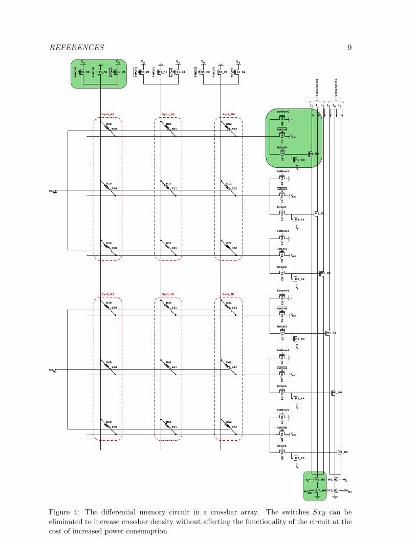
5. Integration into a crossbar array
There are several applications where area is an important concern, and dense 2Dsynaptic arrays are desired.
The circuits presented can be integrated in a dense crossbar array by taking apartthe circuit shown in Fig 3 and rearranging them as illustrated in Fig 4. The crossbarcircuit shown in Fig 3 has 6 synapses implemented in a 6× 3 crossbar array connectedto two neurons, where each synapse comprises a three device memory cell. The circuitelements implementing the proposed normalizer circuits are highlighted in green andlabeled to match to the corresponding circuit elements in Fig. 3. In this design, circuitselements are shared by multiple synapses. That is, all the memristive devices in acolumn, Cx, share the transistors S1_Cx, S3_Cx, and S5_Cx. All the memristivedevices in a row, Rx, share the transistors S2_Rx, S4_Rx, and S6_Rx. The normalizerbias circuits comprising, M5_Nx and S13_Nx, are shared by all synapses associated

REFERENCES 8
with neuron Nx. When a synapse, Synx_Ny is read, the three devices in it are put in aconfiguration equivalent to the one shown in Fig. 3 with n = 3. In Fig 4, each memristivedevice, Dxy, has a series access transistor, Sxy, that prevents flow of current throughinactive synapses. This transistor can be eliminated to increase crossbar density withoutaffecting the functionality of the circuit at the cost of increased power consumption.
Read operation : When a spike train addressed to neuron Ni arrives, the correspondingSelNi signal turns on the the switches Sxy of the synapses afferent to the neuron.Transistors S1_Cx and S2_Ry corresponding to the neuron Ni are also turned on. Thisconnects all the synapses belong to neuron Ni to its normalizer bias circuit. By theprinciple of linear super-position. Even though all synapses share the same normalizerbias block, the current read out of the normalizer is the same as that generated if eachsynapse had its own normalizer block.
Write operation : At the end of the read operation, all the synapses are updated asper the directions of the learning block or the downstream neuron. However, unlike thedifferential memristive synapse circuit, described in Sec ??, a subset of the synapsescannot be programmed while part of it is being read. The write operation in thisarrangement requires a controller that issues a sequence of signals that gates all readactivity while the state of the crossbar array is being updated. The entire array can beupdated in two phases. In the first phase, all those device whose conductances need tobe increased are updated by enabling to corresponding SetColx and SetRowy signals.In the next phase, the devices whose conductances are to be decreased are programmedby programming the ResetColx and ResetRowy signals. Similar update schemes havealso been proposed in earlier works such as [4, 5].
References
[1] E. Chicca et al. “Neuromorphic electronic circuits for building autonomous cognitivesystems”. In: Proceedings of the IEEE 102.9 (Sept. 2014), pp. 1367–1388. issn: 0018-9219.
[2] G. Indiveri et al. “Neuromorphic silicon neuron circuits”. In: Frontiers in Neuroscience 5(2011), pp. 1–23. issn: 1662-453X.
[3] L. Müller, M. Nair, and G. Indiveri. “Randomized Unregulated Step Descent for LimitedPrecision Synaptic Elements”. In: International Symposium on Circuits and Systems,(ISCAS), 2017. submitted. IEEE. 2017.
[4] Manu V Nair and Piotr Dudek. “Gradient-descent-based learning in memristive crossbararrays”. In: Neural Networks (IJCNN), 2015 International Joint Conference on. IEEE.2015, pp. 1–7.
[5] Mirko Prezioso et al. “Training and operation of an integrated neuromorphic networkbased on metal-oxide memristors”. In: Nature 521.7550 (2015), pp. 61–64.
[6] Robert Urbanczik and Walter Senn. “Learning by the dendritic prediction of somaticspiking”. In: Neuron 81.3 (2014), pp. 521–528.
REFERENCES 9
S5_C0S
etC
ol0
S3_C0
Rst
Co
l0
S1_C0
Rd
Co
l0
S5_C1
SetC
ol1
S3_C1
Rst
Co
l1
S1_C1
Rd
Co
l1
S5_C2
SetC
ol2
S3_C2
Rst
Co
l2
S1_C2
Rd
Co
l2
S6
_R
0
SetRow0
S4
_R
0
RstCol0
S2
_R
0
RdCol0
M2_R0
M1_R0
S6
_R
1
SetRow1
S4
_R
1
RstCol1
S2
_R
1
RdCol1
M2_R1
M1_R1
S6
_R
2
SetRow2
S4
_R
2
RstCol2
S2
_R
2
RdCol2
M2_R2
M1_R2
S6
_R
3
SetRow3
S4
_R
3
RstCol3
S2
_R
3
RdCol3
M2_R3
M1_R3
S6
_R
4
SetRow4
S4
_R
4
RstCol4
S2
_R
4
RdCol4
M2_R4
M1_R4
S6
_R
5
SetRow5
S4
_R
5
RstCol5
S2
_R
5
RdCol5
M2_R5
M1_R5
S13_N0
M5_N0
S13_N1
M5_N1Vb
SelN0
Vb
SelN1
I0
I1
I2
I3
I4
I5
To
Neu
ron
N0
To
Neu
ron
N1
SelN0
SelN1
D00
S00
D10
S10
D20
S20
D30
S30
D40
S40
D50
S50
D01
S01
D11
S11
D21
S21
D31
S31
D41
S41
D51
S51
D02
S02
D12
S12
D22
S22
D32
S32
D42
S42
D52
S52
Vs
Vs
Vs
Vs
Vs
Vs
Syn0_N0 Syn1_N0 Syn2_N0
Syn0_N1 Syn1_N1 Syn2_N1
Vrst
Vrst
Vrst
Vrst
Vrst
Vrst
Vst
Vrd
Vst
Vrd
Vst
Vrd
Figure 4: The differential memory circuit in a crossbar array. The switches Sxy can beeliminated to increase crossbar density without affecting the functionality of the circuit at thecost of increased power consumption.