A DC -DC Charge Pump Based on Voltage Doubler spedesign/.../Papers_2011/chargePump_area.pdf · A DC...
24
A DC-DC Charge Pump Based on Voltage Doublers 1 Janusz A. Starzyk and Ying-Wei Jan Abstract- A new organization of switched capacitor charge pump circuits based on voltage doubler structures is presented in this paper. Each voltage doubler takes a DC input and outputs a doubled DC voltage. By cascading n voltage doublers the output voltage increases up to 2 n times. A two phase and a multiphase voltage doubler structures are proposed and their properties discussed. The multiphase voltage charge pump is a minimum capacitance realization of the switched-capacitor based voltage multiplier. A simulator working in the Q-V realm was used for simplified circuit level simulation and to estimate the number of required clock cycles to pump the output to a desired voltage. In order to evaluate the power delivered by a charge pump, a resistive load is attached to the output of the charge pump and an equivalent capacitance is evaluated. Power analysis is performed using an equivalent R-C circuit. A comparison of the proposed circuits with Dickson charge pump and Makowski’s voltage multiplier is presented in terms of the area requirements, the voltage gain, and the power level. This paper also shows the results of computer simulation that identifies optimum loading conditions for different configurations of the charge pumps. Design guidelines for the desired voltage and power levels are discussed. I. INTRODUCTION A charge pump circuit provides a voltage that is higher than the voltage of the power supply or a voltage of reverse polarity. In many applications such as Power IC, continuous time filters, and EEPROM, voltages higher than the power supplies are frequently required. Increased voltage levels are obtained in a charge pump as a result of transferring charges to a capacitive load and do not involve amplifiers or transformers. For that reason a charge pump is a device of choice in semiconductor technology where normal range of operating voltages is limited. Charge pumps usually operate at high frequency level in order to increase their output power within a reasonable size of total capacitance used for charge transfer. This operating frequency may be adjusted by compensating for changes in the power requirements and saving the energy delivered to the charge pump. Among many approaches to the charge pump design, the switched-capacitor circuits such as Dickson charge pump [1] are very popular, because they can be implemented on the same chip together with other components of an integrated system. Many research works focused on the design and timing scheme of Dickson charge pump had been accomplished such as [2]-[5]. Witters et al. [2] provided a detailed analysis of Dickson multiplier built in VLSI technology with diodes realized by nMOS transistors. They considered effects of threshold voltage and leakage current as well as conducted a number of experimental measurements. Cataldo and Palumbo [3] presented an optimized design methodology for double and triple charge pumps, and in [4] they discussed a dynamic model of n-stage Dickson charge pump useful for a pencil and paper design. In [5] Tanzawa and Tanaka provided a detailed 1 1 The authors are with School of Electrical Engineering and Computer Science, Ohio University, Athens, Ohio, 45701.
-
Upload
dinhkhuong -
Category
Documents
-
view
221 -
download
0
Transcript of A DC -DC Charge Pump Based on Voltage Doubler spedesign/.../Papers_2011/chargePump_area.pdf · A DC...

A DC-DC Charge Pump Based on Voltage Doublers
1Janusz A. Starzyk and Ying-Wei Jan
Abstract- A new organization of switched capacitor charge pump circuits based on voltage doubler structures is
presented in this paper. Each voltage doubler takes a DC input and outputs a doubled DC voltage. By cascading n
voltage doublers the output voltage increases up to 2n times. A two phase and a multiphase voltage doubler
structures are proposed and their properties discussed. The multiphase voltage charge pump is a minimum
capacitance realization of the switched-capacitor based voltage multiplier. A simulator working in the Q-V realm
was used for simplified circuit level simulation and to estimate the number of required clock cycles to pump the
output to a desired voltage. In order to evaluate the power delivered by a charge pump, a resistive load is attached
to the output of the charge pump and an equivalent capacitance is evaluated. Power analysis is performed using an
equivalent R-C circuit. A comparison of the proposed circuits with Dickson charge pump and Makowski’s voltage
multiplier is presented in terms of the area requirements, the voltage gain, and the power level. This paper also shows
the results of computer simulation that identifies optimum loading conditions for different configurations of the
charge pumps. Design guidelines for the desired voltage and power levels are discussed.
I. INTRODUCTION
A charge pump circuit provides a voltage that is higher than the voltage of the power supply or a voltage of
reverse polarity. In many applications such as Power IC, continuous time filters, and EEPROM, voltages higher than
the power supplies are frequently required. Increased voltage levels are obtained in a charge pump as a result of
transferring charges to a capacitive load and do not involve amplifiers or transformers. For that reason a charge
pump is a device of choice in semiconductor technology where normal range of operating voltages is limited. Charge
pumps usually operate at high frequency level in order to increase their output power within a reasonable size of total
capacitance used for charge transfer. This operating frequency may be adjusted by compensating for changes in the
power requirements and saving the energy delivered to the charge pump.
Among many approaches to the charge pump design, the switched-capacitor circuits such as Dickson charge
pump [1] are very popular, because they can be implemented on the same chip together with other components of an
integrated system. Many research works focused on the design and timing scheme of Dickson charge pump had been
accomplished such as [2]-[5]. Witters et al. [2] provided a detailed analysis of Dickson multiplier built in VLSI
technology with diodes realized by nMOS transistors. They considered effects of threshold voltage and leakage
current as well as conducted a number of experimental measurements. Cataldo and Palumbo [3] presented an
optimized design methodology for double and triple charge pumps, and in [4] they discussed a dynamic model of
n-stage Dickson charge pump useful for a pencil and paper design. In [5] Tanzawa and Tanaka provided a detailed
1
1 The authors are with School of Electrical Engineering and Computer Science, Ohio University, Athens, Ohio, 45701.
dynamic analysis of Dickson pump and derived analytical expressions for the rise time and current consumption.
They also estimated boosting energy and the optimum number of stages to minimize the rise time. The voltage gain
of Dickson charge pump is proportional to the number of stages in the pump. It may cost quite many devices and
silicon area, when a charge pump with the voltage gain larger than 10 or 20 is needed. Such high voltage gains are
required for low voltage EEPROMs, and typically more than three stages of Dickson charge pump are used.
Improved Dickson charge pumps for low voltage EEPROMs and flash memories were developed and discussed in
[6]-[8]. Authors in [6] proposed the negative gate biased source erase scheme and supporting circuitry. The pulse
timing was adjusted to maintain high efficiency of energy transfer. For a large voltage gain, Makowski [9]
introduced an n stages charge pump with its final voltage gain limited by (n+1)th Fibonacci number. In [9] the
following Fibonacci sequence is used : 1, 2, 3, 5, 8, 13, 21, 34, 55, 89, 144, 233 ... . For instance a 4-stage
Makowski charge pump would have the maximum voltage gain equal to 8, a 5-stage would have the voltage gain of
13, e.t.c.. Researchers have focused on different issues related to practical implementation of the charge pump
starting from its topological properties [9], voltage gain, and dynamic properties [5] to improvements in efficiency
and power considerations [10].
Charge pump operates by switching on and off a large number of MOS switches which charge and
discharge a large number of capacitances, transferring energy to the output load. Large amount of energy is lost
whenever the load current is reduced. Savings of switching energy were primary reason for the design efforts
presented in [10], where a special circuit organization was proposed to regulate switching frequency whenever a
requirement for the load current changes. In addition, simulation and measurement results presented in [10]
indicated a strong dependence of the output voltage on the load resistance. There is a need for better understanding
of the design tradeoffs related to charge pump design.
This paper presents switched-capacitor charge pumps which have exponentially growing voltage gain as a
function of the number of stages. The proposed charge pumps are constructed by several cascaded voltage doublers,
with n cascaded voltage doublers providing the voltage gain of up to 2n. The circuits of the voltage doublers are
analyzed in Section II and topological method introduced by Makowski is used to show that the charge transfer
produces the expected growth in the voltage level. Section III shows the computer simulation results of the proposed
charge pumps and the comparison with the Dickson charge pump and the Makowski charge pump. Design
considerations of the charge pumps based on the proposed organization are included in Section IV were tradeoffs
between power, frequency, and voltage level are addressed. An optimum load termination is discussed using a
resistive load model. Recommendations for the optimum loading conditions are expressed as a function of output
power and voltage levels. Section V discusses power, timing and frequency issues in a limited designed area.
Section VI presents the conclusion.
II. VOLTAGE DOUBLERS
A switched-capacitor organization of a two phase DC-DC voltage doubler is shown in Fig. 1. It contains 2
clock controlled switches and 2 capacitors. For a simple explanation of the voltage doubler operation, let us assume
that the switches and capacitors are all ideal. That is, we assume that there is no leakage current in capacitors,
switches dissipate no energy and the electric charge transferring is instantaneous. Fig. 2 (a) shows the equivalent
2
circuit of the voltage doubler, when the circuit is in the kth iteration cycle and the clock is in phase 1. At this time
instance, the load capacitor CL holds the previous voltage value.
. (1)Vout[k] = Vout
[k−1]
The voltage across the capacitor CS changes from to Vin. The charge transferred from the−(V in − Vout[k−1]) DQ[k]
voltage source Vin to Cs is obtained from
. (2)DQ[k] = Cs( V in − (−(Vin − Vout[k−1])) ) = Cs(2Vin − Vout
[k] )
Equation (2) implies that the voltage source Vin would stop transferring charge to Cs if .Vout[k] = 2V in
Fig. 2 (b) shows the equivalent circuit of the voltage doubler when the circuit is in the (k+1)th iteration
cycle and the clock is in phase 2. According to the charge conservation law at the node connecting CL and CS, and
evaluating charges stored in capacitors as Q = C V, the relationship between voltages at kth and (k+1)th iteration can
be expressed by
. (3)V in % Cs + Vout[k] % CL = (Vout
[k+1] − V in) % Cs + Vout[k+1] % CL
If we set , to represent the capacitor ratio, then r = Cs
CL+Cs
, (4)Vout[k+1] = (1 − r)Vout
[k] + 2rV in
where 0 < r < 1. Thus, Vout can be represented as a sequence of the iteration index k. The values of the output to
input voltage ratio (voltage gain) in different iterations k are shown in Table 1. It is assumed that initialAv = VoutVin
state of the voltage doubler is =0.Vout[0]
§§1(8r-12r2+8r3-2r4)(1-r)+2r = 2[1-(1-r)5]112(8r-12r2+8r3-2r4)(1-r)+2r = 2[1-(1-r)5] 101(6r-6r2+2r3)(1-r)+2r = 2[1-(1-r)4] 92(6r-6r2+2r3)(1-r)+2r = 2[1-(1-r)4] 81(4r-2r2)(1-r)+2r = 2[1-(1-r)3] 72(4r-2r2)(1-r)+2r = 2[1-(1-r)3] 612r(1-r)+2r = 2[1-(1-r)2] 522r(1-r)+2r = 2[1-(1-r)2] 412r = 2[1-(1-r)1] 322r = 2[1-(1-r)1] 2101200
phaseAvk
Table 1. The voltage gain at incremented iteration index k and changing clock phases.
It is easy to find the limit value of the voltage doubler’s gain Av from the symbolic expressions in the Table
1. We can also calculate the limit gain value for the voltage doubler using a theoretical study of switched-capacitor
voltage multipliers by Makowski [9]. Fig. 3 shows the voltage gains Av as a function of the iteration index k, with
different r. The smaller the r, the larger the ratio of the grounded capacitor CL to the switched capacitor Cs. It is
clear that the final (steady state) value of the voltage gain Av is 2 independently of the capacitor ratio r. That is, the
circuit in Fig. 1 works as a voltage doubler provided that the voltage source Vin supplies enough charge to the charge
3
pump. The larger CL (smaller r) requires more clock cycles (bigger k) to reach the desired output voltage. The value
of r does not influence the final voltage gain.
Another way to verify that the circuit in Fig. 1 has the voltage gain of two is to apply the approach
presented by Makowski in [9]. Makowski’s analysis provides a compact theoretical solution to any two phase
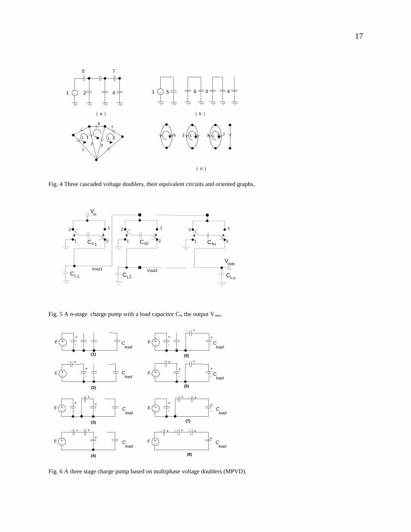
switched-capcitor based voltage multiplier. The equivalent circuit of three cascaded voltage doublers in the
switching phase 2 is illustrated in Fig. 4 (a), and its graph is shown in Fig. 4 (c). Fig. 4 (b) shows the equivalent
circuit in the switching phase 1, and its graph is shown in Fig. 4 (d). The basic loopset matrix of the graph in Fig. 4
(c) is
, (5)B1 =loops o L1
L2L3
edgesd
1 2 3 4 5 6 7
1 −1 0 0 1 0 00 1 −1 0 0 1 00 0 1 −1 0 0 1
= [B1t 1]
and the basic loopset matrix of the graph in Fig. 4 (d) is
. (6)B2 =loops o L1
L2L3
edgesd
1 2 3 4 5 6 7
−1 0 0 0 1 0 00 −1 0 0 0 1 00 0 −1 0 0 0 1
= [B2t 1]
According to [9], the ideal output voltage conversion ratio is obtained by evaluating the difference of the two
submatrices of the loopset matrices which correspond to the selected tree:
. (7)DDB = B1t − B2
t =1 −1 0 00 1 −1 00 0 1 −1
−−1 0 0 0
0 −1 0 00 0 −1 0
=2 −1 0 00 2 −1 00 0 2 −1
Then, using Binet-Cauchy theorem we can find the maximum voltage gain from the ratio of two major cofactors of
∆∆B:
(8)M = −
det
2 −1 00 2 −10 0 2
det
−1 0 02 −1 00 2 −1
= 81 = 8.
Using the same topological technique, we can verify that a charge pump with 4 cascaded voltage doublers will have a
maximum voltage gain equal to 16, 5 doublers will have a gain of 32, and so on. General organization of n-stage
voltage doublers charge pump is shown in Fig. 5.
While the presented design does not provide a maximum theoretical gain determined by the upper bounds
set by Makowski’s work, it yields a regular and efficient structure with the output voltage level compatible with a
4

binary system. By using different powers of two and a switched-capacitor adder, any integer level voltage can be
precisely set by using a small number of stages of voltage doublers.
In his study of switched-capacitor voltage multiplier circuits [9] Makowski established a theoretical limit on
the voltage gain in a two-phase multiplier and related it to Fibonacci numbers. A question which was not answered
by his work is if higher voltage gains can be attained in multiphase circuits. We would like to address this issue in
this paper by first proving the theoretical limit for voltage gain in multiphase multipliers and then by constructing a
multiplier with the maximum gain. The following conjecture sets the voltage gain limit.
Conjecture - The realizable conversion ratio of a multiphase DC-DC switched-capacitor voltage multipler with a
single voltage source without transformers is limited by
, (9)M nVV
out
in
n( ) = = 2
where M(n) is the maximum voltage gain for the multiplier with n capacitances, Vout is the output DC voltage and Vin
is the input (source) DC voltage.
Proof (by induction): For n=1 (a single capacitor and the voltage source) the largest gain is 2 - this fact can be
easily established by construction. Assume that for n capacitors and a voltage source with ideal switches used to
reconfigure capacitor connections, the largest gain is 2n. Then an additional capacitance can be charged to the
maximum voltage Vmax(n) not larger than 2nVin. After charging this additional capacitance to its maximum attainable
voltage Vmax(n), the largest voltage possible is obtained by adding the previously established largest voltage and the
voltage obtained on the additional capacitance. The result is not larger than 2n+1Vin, which constitutes a proof for the
upper limit of the voltage gain.
By constructing a network which reaches this upper limit, we can demonstrate that the limit is an attainable
upper bound. An example organization of the multiphase charge pump with the voltage gain equal to the upper
bound is shown in Fig. 6. This circuit includes 4 switches per a single capacitor, therefore it exceeds the upper limit
on a number of switches per capacitor for a two phase voltage multiplier that was estimated in [9] as not more than
3-2/n. In addition, the maximum gain structure requires nonoverlapping clocks of different frequencies to control
these switches. However, MOS switches designed in the charge pumps use much smaller area than capacitors and
are not detrimental for the pump performance.
Fig. 6 shows a three stages charge pump based on the multiphase voltage doublers. This charge pump is
constructed by 3 internal capacitors, and attains the voltage gain of 8. At the output of this charge pump, the load
capacitor Cload is used to accumulate the charge. There are eight different states of internal capacitors
interconnection used to control the flow of electric charge. Each internal capacitor works as a voltage doubler. The
working of this charge pump begins at state (1), then goes to (2) , (3) ,..., (8) and then goes back to state (1) and the
cycle is repeated. If the voltage controlled switches are used to implement this charge pump, 3 different frequencies
of clocked signals are required.
5
III. CIRCUITS DESIGN AND SIMULATION
The circuit in Fig. 1 can double the input DC voltage regardless the sizes of internal capacitors. The
capacitor sizes only effect the rise time needed for transferring enough charges to the output load. This is under the
assumption that the circuit is ideal - no dissipation of energy in the switches, no leakage current, and no resistive
load. Because it works with the two phase clock we call this structure a two phase voltage doubler (TPVD) in
differentiation to the circuit presented in Fig. 6 which is identified as a multiphase voltage doubler (MPVD).
It might be really exhausting to do an exact symbolic analysis of voltage multiplier circuits based on the
approach presented in [9] for larger number of multiplier sections, when a significant voltage gain is needed. In
addition, the analysis presented in [9] deals only with purely capacitive networks, so the resistive load considerations
will be very difficult using symbolic analysis. To observe the behavior of n-stage charge pumps, shown in Figs. 5
and 6, a computer simulation program based on Q-V realm analysis was developed and used in analysis of this
charge pump circuit. This program called SAMOC (for Switched-capacitor Analysis of MOS Circuits), generates
the charge conservation equations at capacitive nodes, and uses modified nodal-like equations for independent and
voltage controlled voltage sources, ideal switches, and ideal diodes. The Q-V realm analysis is accomplished by
solving the charge conservation equations:
C V = Q, (10)
where C is the modified nodal capacitance matrix, V is the voltage vector, Q is the initial charge vector. The circuit
description that SAMOC can recognize is similar to the SPICE input format, which facilitates generation and reading
of large data files. Transistor level netlists obtained from synthesis programs can be directly fed to SAMOC for
analysis. The program is written for large networks with MOS switches and employs event driven simulation with
circuit partitioning. Separate subcircuits are obtained for charge transfer analysis and a resistive type DC analysis is
performed on the subnetwork level.
Fig. 7 shows the simulated outputs V(CL) at each stage of the 4 cascaded TPVDs. The total number of clock
cycles in this simulation is 750 (1500 iterations considering two iterations per clock cycle) and CL = CS =100 pF,
that is, the capacitor ratio r = 0.5. In this simulation, the input voltage Vin is 5V. The simulation results show that
V(CL1)=Vout1 = 10V, V(CL2)=Vout2 = 20V, V(CL3)=Vout3 = 40V, and V(CL4)=Vout4 approaches 80V.
SPICE simulation of the TPVD charge pump was performed in order to compare with SAMOC for
accuracy and computing efficiency. Since SPICE neither supports pure floating capacitors nor ideal switches,
additional resistors are added in order to make the SPICE simulation feasible. A 1010 Ω leakage resistor is added in
parallel with each floating Cs capacitor in TPVD charge pump. The turned-on resistance ( Ron ) of all the voltage
control switches is 1 Ω, and the turned-off resistance ( Roff ) is 107 Ω. In SAMOC simulation, there is no leakage
resistor of capacitor, and ideal switches have Ron = 0 Ω and Roff = ∞ Ω. Fig. 8 shows both the SAMOC and SPICE
simulations. The clock period is 40ns. Both SPICE and SAMOC show very similar results at the beginning of the
simulation. The leakage resistance of capacitors and turned-off resistance of switches resulted in the pump reaching
lower voltage value in SPICE simulation. The SPICE simulation was performed by MicroSim PSPICE which
6
works in Microsoft Windows 95, the same platform as SAMOC. The two simulators were run on the same
computer with the same operating system for comparison of timing efficiency. SPICE took 121.3 sec to simulate a
three stage voltage doubler, while SAMOC required only 1.3 sec. This time difference, which indicated high
performance of SAMOC program, grows significantly larger if SPICE is run using full models of MOS switches.
Full SPICE analysis with parasitic values extracted from a layout of designed pump has to be performed at the design
stage of a silicon charge pump. However, this analysis is extremely costly to do for the type of investigation
conducted in this work. For this reason, analysis using SAMOC is fully justified and facilitates study of the
fundamental properties of the proposed pumps.
To compare the proposed charge pumps with the Dickson charge pump [1] and the Makowski
(Fibonacci-sequence) charge pump [9], we chose charge pump with the voltage gain AV = 7. For the specific voltage
gain the proposed charge pumps require 3 stages, Dickson charge pump requires 8 stages, and Makowski charge
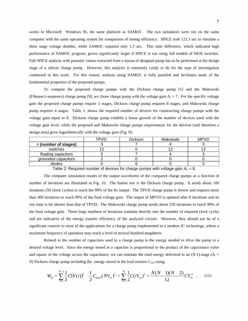
pump requires 4 stages. Table 2. shows the required number of devices for constructing charge pumps with the
voltage gain equal to 8. Dickson charge pump exhibits a linear growth of the number of devices used with the
voltage gain level, while the proposed and Makowski charge pumps requirements for the devices (and therefore a
design area) grow logarithmically with the voltage gain (Fig. 9).
0080diodes0002grounded capacitors3473floating capacitors1212012switches3473n (number of stages)
MPVDMakowskiDicksonTPVD
Table 2: Required number of devices for charge pumps with voltage gain AV = 8.
The computer simulation results of the output waveforms of the compared charge pumps as a function of
number of iterations are illustrated in Fig. 10. The fastest one is the Dickson charge pump. It needs about 100
iterations (50 clock cycles) to reach the 99% of the 8x output. The TPVD charge pump is slower and requires more
than 400 iterations to reach 99% of the final voltage gain. The output of MPVD is updated after 8 iterations and its
rise time is bit shorter than that of TPVD. The Makowski charge pump needs about 250 iterations to reach 99% of
the final voltage gain. These large numbers of iterations translate directly into the number of required clock cycles
and are indicative of the energy transfer efficiency of the analyzed circuits. However, they should not be of a
significant concern to most of the applications for a charge pump implemented in a modern IC technology, where a
maximum frequency of operation may reach a level of several hundred megahertz.
Related to the number of capacitors used in a charge pump is the energy needed to drive the pump to a
desired voltage level. Since the energy stored in a capacitor is proportional to the product of the capacitance value
and square of the voltage across the capacitance, we can estimate the total energy delivered to an (N-1)-stage (Av =
N) Dickson charge pump including the energy stored in the load resistor Cload using:
, (11)W C V i C NV C iVN N N
CVDi
N
load ini
N
in in= + = =+ +
=
−
=∑ ∑1
2
1
2
1
2
1 2
122
1
12
1
2 2[ ( )] ( ) ( )( )( )
7

where in order to simplify discussion we assumed that C=Cload. By comparison, the total energy delivered to an
M-stage TPVD charge pump with the same voltage gain ( Av = N ) can be estimated from
,(12a)W C V C VC
V V CVp s C i L C ii
ini
in
M
i
M
i
M
ins L12 2 2 1 2
11
212 2
2 25 4 1
6= + = + =
−−
==∑∑ ( ) [( ) ( ) ]
( )
while assuming Csi = CLi.= C. For the MPVD charge pump with the same voltage gain the delivered energy can
estimated by
. (12b)W CV C VC
V CVp ii
M
load outi
ini
M M
in22
1
2 2
0
121
2 22
4 16
= + = =−
= =
+
∑ ∑[ ] ( )( )
while Cload = C. Since the number of stages M=log2(N), the total energy used to drive the output of the TPVD charge
pump to the equivalent voltage level equals to
(13a)W N CVp in12 25
61= −( )
for TPVD charge pump, and
(13b)W N CVp in22 21
64 1= −( )
for MPVD charge pump. In the above equations we considered all capacitances in both pumps of equal values. As
we can see from the obtained results the boosting energy increases quadraticly with the voltage gain in TPVD charge
pump as opposed to the cubic increase in Dickson charge pump. The boosting energy is roughly 25% higher in the
TPVD charge pump than in the equivalent MPVD charge pump, although the number of capacitors MPVD uses is
half of that used in the TPVD pump of the same voltage gain. Fig. 11 shows the boosting energy as a function of the
voltage gain for these three charge pumps. Dickson charge pump requires much more boosting energy then
proposed ones for the high voltage gains.
8
IV. OPTIMIZED POWER TRANSFER CONSIDERATIONS
The charge pump circuit analysis and the simulation results presented so far are obtained under the
assumption that there is no power loss in the charge pump circuits, and that the electric charge transfer is
instantaneous. After the output of such a charge pump reaches its maximum voltage level, there will be no energy
driven from the supply source. In the real world application, charge pumps will deliver charges to capacitive loads
with a finite leakage resistance or will be used to drive electronic devices that can be treated as resistive loads. If
there is a resistive load at the output of the charge pump, then the electric power will be dissipated by the load
resistor. In such case, the law of charge conservation which is used in the Q-V realm analysis is no longer
applicable. One simple way to estimate the effect of the resistive load on the operation of a charge pump is to solve
the output circuit equation considering the output resistance Rload and the equivalent charge pump circuit (shown in
Fig. 12(a). By estimating the equivalent capacitance Ceq, the electric charge dissipated by the load resistor Rload
during a clock period can be evaluated from
, (14)Q V CT
R CR o eqload eq
= − −( exp( ))1
where Vo is the output voltage when Rload is absent (Fig. 12b), and T is the clock period.
After evaluating QR we can modify the Q-V realm equations as follows:
CV =Q - QR d, (15)
where d is the selection vector, Vout = d t V =VR . That is, the load resistor in the Q-V realm analysis is treated as a
voltage dependent charge drain which removes electric charge from the equivalent capacitance Ceq. The power PR
dissipated by Rload (delivered by the charge pump) can be estimated by
. (16)P V IVRR R R
R
load
= =2
The equivalent capacitance Ceq is estimated by putting a dummy voltage source Vd = 0V in the output (see Fig. 12c).
The electric charge Qd, goes through the dummy voltage source and can be obtained from simulation of the shorted
charge pump formulating the modified nodal-like equations. Then the equivalent capacitance Ceq can be estimated
using
, (17)CQVeq
d
o
=
where Vo is the open circuit output voltage used in (14).
The resistive load analysis requires 2 Q-V realm analyses in each clock phase instance. The first one is to
evaluate the equivalent capacitance Ceq, and the second one is to calculate the effect caused by removing QR from the
output of the charge pump (14). In order to understand the effect of the resistive load on the output voltage and the
amount of the output power delivered, a TPVD charge pump with 4 cascaded voltage doublers was used for resistive
9

load analysis with different values of the load resistance, Rload. The capacitors CL and CS are 100pF, and the clock
period T is 40ns with power supply 5V. The load resistances used were 2kΩ, 20kΩ, 200kΩ and infinity. Fig. 13
shows the simulation results for the first 1500 iterations.
In the plot, we can find out that the charge pump can no longer supply the 16x output, while the Rload is
present. The load resistor Rload would drain the electric charge supplied by the charge pump. The loss of electric
charge decreases the output voltage of the charge pump. The smaller the Rload , the more electric charge, QR, is
drained by Rload during the clock period, and the lower the output voltage is.
The resistive load analysis can be used to estimate the output power of a charge pump according to different
values of Rload and output voltages. To obtain the power and output voltage characteristics of a charge pump, Rload
values from 100 Ω~ 1 mega Ω were used in simulation.
The SAMOC simulation results, which show the TPVD charge pumps voltage outputs VR, for 2, 3 and 4
voltage doublers as a function of the load resistor Rload, are plotted in Fig. 14. This plot can be used to design a
charge pump working with a specific load resistance and a desired voltage level. The power delivered by the charge
pump PR as a function of Rload is plotted in Fig. 15, while Fig. 16 shows VR as a function of the output power PR. We
can find out that a charge pump delivers a maximum power when a specific value of Rload is applied to its output, and
that at this optimum load the output voltage drops to one half of its maximum value measured on the open circuit
output terminals. In the simulation, the TPVD charge pump with 2 voltage doublers shows a maximum output power
equal to 38.8mW for the load resistance Rload = 3k Ω and all the capacitors in the charge pump equal to 100pF. The
TPVD charge pump with 3 voltage doublers has the maximum output power equal to 38.5mW for Rload = 10kΩ, and
the charge pump with 4 voltage doublers has a maximum output power equal to 37.6mW, for Rload = 42.4kΩ. The
larger the number of the voltage doublers the bigger the output voltage. As we can observe from the results the of
circuit analysis, increasing the number of voltage doublers does not have a strong effect on the maximum output
power delivered by the charge pump. This power is a function of energy transport efficiency and depends mainly on
the capacitance sizes and the clock frequency.
Fig. 17 describes changes of the power delivered to the optimum load for different sizes of charge pump
capacitors at a fixed output voltage level. Fig. 18-20 show relation between the output voltage, output power and
load resistance at various sizes of pump capacitors. output voltage level in a 2-stage TPVD charge pump.
As we can see from Fig. 17 the growth of the optimum output power is linear with the capacitance size.
Since the optimum power is obtained at the same voltage level for a given charge pump, we can find dependence
between the output power level and the optimum load resistance using:
(18)PVR
KC RVKCo
out
loadload
out= = ⇒ =2 2
where K is a constant for a given charge pump organization (in the TPVD design K~0.385 mW/pF). This indicates
that the optimum load resistor is in inverse proportion to the values of the charge pump capacitance used. For
10
instance, if the charge pump with two voltage doublers will use 100pF capacitors then the maximum power
transferred to the load will be 38.5 mW and the optimum load resistance can be estimated as
. (18a)RVKC
vkload
out= = =2 2 220 2
38 52 6
( / )
..
mWΩ
This dependence of the load resistance on the size of pump capacitances can be observed across the entire
range of output voltages - the larger the capacitors used, the smaller the optimum load resistance needed to support a
constant output voltage on the load terminated charge pump as can be observed in Fig. 18. Fig. 19 shows
dependence of the output power as a function of load resistance for different sizes of charge pump capacitances. We
see both the increase of the maximum power delivered to the load as well as the reduction of the optimum load
resistance value for increasing values of capacitances used in the charge pump. Finally, Fig. 20 shows dependence
between output voltage and power.
By simulating the proposed charge pumps with different voltage gains we were able to generate design
curves, which can be helpful in deciding about loading conditions for various voltage gains and required power. The
results shown in Fig. 21 indicate almost linear dependence between voltage gain, optimum load resistance, and
maximum power delivered to the load, and can be extrapolated with large accuracy for regions outside of the
simulated area.
To compare the load effect on different charge pumps we simulated the proposed charge pumps both TPVD
and MPVD with 3 stages, Dickson charge pump with 7 stages, and Makowski charge pump with 4 stages. The
output voltage characteristics of the compared charge pumps as functions of the load resistance are shown in Fig. 22.
We observe that the same voltage level was reached at different load resistance values. This would indicate different
power driving capabilities of these designs and almost exactly corresponds to the shift in the optimum load resistance
in the proposed designs observed in Fig. 18 for increased capacitance values.
Fig. 23 illustrates the output power of these four different charge pumps as a function of load resistance, and
Fig. 24 verifies that the optimum power level was obtained at the output voltage approximately equal to one half of
the maximum voltage level for these circuits (40V). We can find out that the TPVD charge pump has a maximum
output power 38.5 mW when Rload is about 10kΩ. MPVD charge pump has a maximum output power 33.1 mW
when Rload is about 14kΩ. Makowski charge pump has a maximum output power 64.6 mW when Rload is about 6kΩ,
while Dickson charge pump has a maximum output power 134 mW when Rload is about 2.8kΩ. Design
considerations have to include different aspects of delivering a maximum amount of power at the desired voltage
level by a circuit which occupies the least area and can be easily integrated with other digital devices on the same
chip. From the conducted study, it is clear that we can trade the power for the area in designing a charge pump the
larger the area for a given voltage, the larger the output power.
11
V. POWER TIMING AND FREQUENCY CONSIDERATIONS
A modern IC fabrication technology requires realization of the designs with a minimum area and energy
dissipation. It was demonstrated in Section III that the boosting energy requirements of a similarly sized Dickson
charge pump are higher than that of the proposed or Makowski charge pumps. This result was obtained under the
assumption of equal size capacitances in all pumps. If capacitance sizes are adjusted to fit a specified design area
then equations (11)-(13) will change.
It is interesting to observe the voltage gain efficiency of various designs at a restricted amount of silicon
area that the charge pump may use. Let us assume that each charge pump uses capacitors of the same sizes. Assume
for simplicity that all design area is divided into equal size capacitances and that there is no overhead for designing
switches and diodes. We get the following dependence of the capacitor sizes on the voltage gain level in different
designs:
(19)CAAd
v
≈
in Dickson charge pump
(20)CA
Apv
≈RSTα
αlog2
where =2 for TPVD
1 for MPVD
in the proposed charge pumps
(21)CA
F Amv
≈ −1( )
in Makowski charge pump, where F-1(Av) is the inverse of the Fibonacci function at a given voltage gain level.
Applying equations (19) - (21) to the estimates of boosting energy (11) - (13) in different charge pumps, we
can directly express the boosting energy as a function of the voltage gain Vout/Vin = N. The following results show
that in a Dickson charge pump
(22)WN N N
CVN N N A
NV
N NAVD in in in=
+ +=
+ +=
+ +( )( ) ( )( ) ( )( )1 2
12
1 2
12
1 2
122 2 2
and the boosting energy increases quadraticly with the voltage gain. In the TPVD charge pumps, the boosting
energy
(23a)WN
CVN A
NV
N AN
VP in in in1
22
2
2
22
2
25 1
6
5 1
6 2
5 1
12=
−=
−=
−( ) ( )
log
( )
log
and for MPVD ones
12
. (23b)WN
CVN A
NV
N AN
VP in in in2
22
2
2
22
2
24 1
6
4 1
6
4 1
6=
−=
−=
−log
( )
log
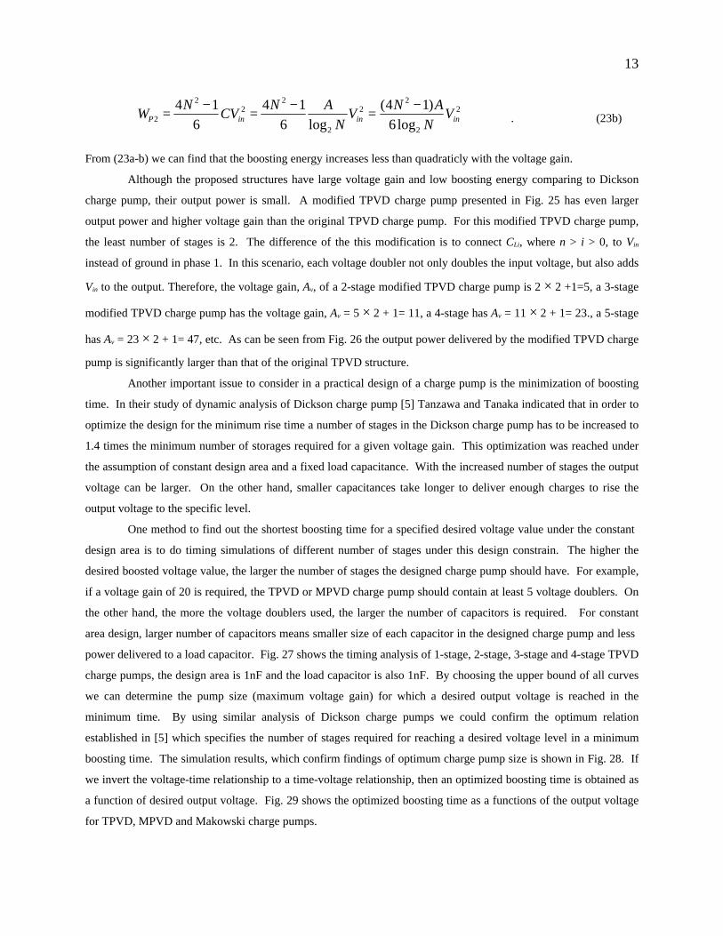
From (23a-b) we can find that the boosting energy increases less than quadraticly with the voltage gain.
Although the proposed structures have large voltage gain and low boosting energy comparing to Dickson
charge pump, their output power is small. A modified TPVD charge pump presented in Fig. 25 has even larger
output power and higher voltage gain than the original TPVD charge pump. For this modified TPVD charge pump,
the least number of stages is 2. The difference of the this modification is to connect CLi, where n > i > 0, to Vin
instead of ground in phase 1. In this scenario, each voltage doubler not only doubles the input voltage, but also adds
Vin to the output. Therefore, the voltage gain, Av, of a 2-stage modified TPVD charge pump is 2 × 2 +1=5, a 3-stage
modified TPVD charge pump has the voltage gain, Av = 5 × 2 + 1= 11, a 4-stage has Av = 11 × 2 + 1= 23., a 5-stage
has Av = 23 × 2 + 1= 47, etc. As can be seen from Fig. 26 the output power delivered by the modified TPVD charge
pump is significantly larger than that of the original TPVD structure.
Another important issue to consider in a practical design of a charge pump is the minimization of boosting
time. In their study of dynamic analysis of Dickson charge pump [5] Tanzawa and Tanaka indicated that in order to
optimize the design for the minimum rise time a number of stages in the Dickson charge pump has to be increased to
1.4 times the minimum number of storages required for a given voltage gain. This optimization was reached under
the assumption of constant design area and a fixed load capacitance. With the increased number of stages the output
voltage can be larger. On the other hand, smaller capacitances take longer to deliver enough charges to rise the
output voltage to the specific level.
One method to find out the shortest boosting time for a specified desired voltage value under the constant
design area is to do timing simulations of different number of stages under this design constrain. The higher the
desired boosted voltage value, the larger the number of stages the designed charge pump should have. For example,
if a voltage gain of 20 is required, the TPVD or MPVD charge pump should contain at least 5 voltage doublers. On
the other hand, the more the voltage doublers used, the larger the number of capacitors is required. For constant
area design, larger number of capacitors means smaller size of each capacitor in the designed charge pump and less
power delivered to a load capacitor. Fig. 27 shows the timing analysis of 1-stage, 2-stage, 3-stage and 4-stage TPVD
charge pumps, the design area is 1nF and the load capacitor is also 1nF. By choosing the upper bound of all curves
we can determine the pump size (maximum voltage gain) for which a desired output voltage is reached in the
minimum time. By using similar analysis of Dickson charge pumps we could confirm the optimum relation
established in [5] which specifies the number of stages required for reaching a desired voltage level in a minimum
boosting time. The simulation results, which confirm findings of optimum charge pump size is shown in Fig. 28. If
we invert the voltage-time relationship to a time-voltage relationship, then an optimized boosting time is obtained as
a function of desired output voltage. Fig. 29 shows the optimized boosting time as a functions of the output voltage
for TPVD, MPVD and Makowski charge pumps.
13
If a constant design area is used, power transfer ability of the proposed as well as Makowski charge pump
improves in relation to Dickson charge pump. Figs. 30 - 31 show the output voltage and power delivered by
different charge pumps as a function of the load resistance for voltage gain of 8, under the assumption of a constant
design area. The total design area for each charge pump is 1 nF and the size of the load capacitor Cload is 10 nF.
Another important issue in charge pump operation is the switching frequency. While charge boosting is
performed at frequencies within 10-30 MHz depending on the desired load current, the frequency should be reduced
to 100 kHz when operating in a standby mode in order to save the energy. A complete study of the switching
frequency in relation to the load requirements was presented in [7]. Frequency regulation should be also related to
transistor sizing for efficient transfer of energy from the source to the load. These issues must be considered at the
practical implementation of the proposed charge pumps in CMOS technology.
VI. Conclusion
New organizations of the switched-capacitor charge pump based on voltage doublers and circuit design
issues are presented and discussed in this paper. The TPVD charge pumps work with 2 inverted clocks similar to
Dickson and Makowski charge pumps. The MPVD charge pumps reach the same voltage gain with the least number
of capacitors, but require more sophisticated clocking scheme. MPVD structure demonstrates a constructive proof
of voltage multipler that reach the theoretical upper bound for a voltage gain in a multiphse switched-capacitor
design with a given number of capacitors. The modified TPVD charge pumps which use more switches, all floating
capacitors offer higher voltage gain and delivery more power to resistive load. The closed form of the voltage gain
for a charge pump with a given number of stages and capacitor ratio r may be difficult to derive, particularly when a
resistive load is considered. Therefore, a computer simulation of the design was performed. By analyzing the
proposed design numerically we observed effects of the resistive load, capacitance ratio, and clock frequency on the
levels of the output voltage and power.
Computer simulation results verified that the proposed charge pumps work as designed. Charge pump
simulation was performed using a Q-V based simulator SAMOC, which produced results equivalent to SPICE
simulation in idealized circuits. Simulator efficiency is two orders of magnitude better than SPICE. Comparing with
two other switched-capacitor charge pumps, Dickson and Makowski, the proposed ones use yet fewer stages but has
longer rising time and deliver relatively less power. In modern IC technology, the additional several hundreds of
clock cycles may not be crucial as it may need less than a few msec. Boosting energy of the proposed charge pump
is generally lower than that of equivalent Dickson charge pumps. The proposed charge pumps may be very useful in
IC circuits that need to use a higher voltage for instance in EEPROM devices.
14

REFERENCES
[1] J. K. Dickson, “On-chip high voltage generation in NMOS integrated circuits using an improved voltagemultiplier technique,” IEEE J. Solid-State Circuits, Vol., SC-11, pp. 374-378, June 1976.
[2] J. S. Witters, G. Groeseneken and H. E. Maes, “Analysis and Modeling of On-Chip High-VoltageGenerator Circuits for Use in EEPROM Circuits” IEEE J. Solid-State Circuits, Vol. 24, No. 5, pp.1372-1380, October 1989.
[3] G. Di Cataldo and G. Palumbo, “Double and Triple Charge Pump for Power IC: Dynamic Models WhichTake Parasitic Effects into Account” IEEE Trans. on .Circuits and Systems -1: Fundamental Theory andApplications, Vol. 40 No. 2. , pp. 92-101, February 1993.
[4] G. Di Cataldo and G. Palumbo, “Design of an Nth Order Dickson Voltage Multiplier”, IEEE Trans. onCircuits and Systems -1: Fundamental Theory and Applications, Vol. 43 No. 5. , pp. 414-418 May 1996.
[5] T. Tanzawa and T. Tanaka, “A Dynamic Analysis of the Dickson Charge Pump”, IEEE J. Solid-StateCircuits, Vol. 32 , No. 8, pp. 1231-1240, August 1997.
[6] A. Umezawa, et al, “ A 5 V-only operation 0.6 µm flash EEPROM with row decoder scheme in triple-wellstructure,” IEEE J. Solid-State Circuits, Vol. 27, pp. 1540-1546, Nov. 1992.
[7] S. Kobayashi, et al, “ A 3.3 V-only 16Mb DINOR flash memory,” ISSCC Dig. Tech. Papers, pp. 122-123,Feb. 1995.
[8] K. Sawada, Y. Sugawara, and S. Masui, “A on-chip high-voltage generator circuit for EEPROM’s with apower supply voltage below 2 V,” in 1995 Symp. VLSI Circuit Dig. Tech. Papers , pp. 75-76, June 1995.
[9] M. S. Makowski, "Realizability Conditions and Bounds on Synthesis of Switched -Capacitor DC-DCVoltage Multiplier Circuits”, IEEE Trans. on Circuits and Systems -1: Fundamental Theory andApplications, Vol. 44 No. 8. , pp. 684-691 August 1997.
[10] C-C. Wang and J-C. Wu, “Efficiency improvement in charge pump circuits”, IEEE Journal of Solid StateCircuits, vol. 32, no. 6 , pp.852-860 June 1997.
15

V
Vout
2
1 2
1
CL
in
Cs
Fig. 1 The DC-DC TPVD voltage doubler.
Vin
-
C
Vout
L
[k+1]∆Q [k]
(a)
Vout
CL
[k]
Vin+
-
Cs
(b)
+
-
+
-Vin
Fig. 2 The equivalent circuits in two clock phases.
0 100 200 300 400 5000
0.5
1
1.5
2
r=0.01r=0.05
r=0.5
clock index k
volta
ge g
ain
Fig. 3 The voltage gain as a function of the clock index k.
16
5 7
2 41 - 1 - 5 6 3 4
L 1 L 3
12 3
67
L 2 L 35 2 3 7
( a ) ( b )
( d )
Fig. 4 Three cascaded voltage doublers, their equivalent circuits and oriented graphs.
V
2
1 2
1
CL
in
Cs
2
1 2
1
CL
Cs2
1 2
Vout
2
1 2
1
CL
Cs
n
n1
Vout1 Vout2
n
Fig. 5 A n-stage charge pump with a load capacitor Cln the output Voutn.
+- C
load
+
-E
+-
Cload
+-
E+
-
+- C
load
+
-E
+-
+
-
+- C
loadE
+-
+
-
+-
+- C
load
+
-E
- +
+
-
+- C
loadE
- +
+
-
+-
+
-
+- C
load
+
-E
+- - +
+
-
+- C
loadE
+-
+
-
+-+-
(1)
(2)
(3)
(4)
(5)
(6)
(7)
(8)
Fig. 6 A three stage charge pump based on multiphase voltage doublers (MPVD).
17
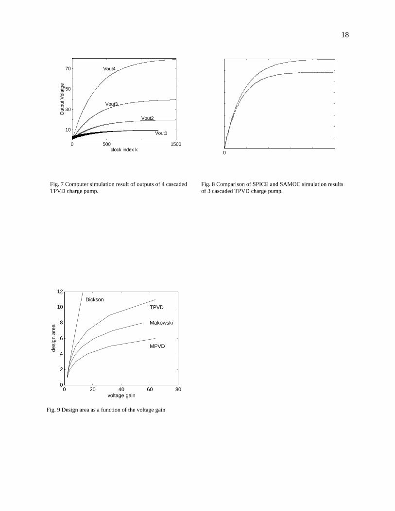
Fig. 8 Comparison of SPICE and SAMOC simulation resultsof 3 cascaded TPVD charge pump.
Fig. 7 Computer simulation result of outputs of 4 cascadedTPVD charge pump.
0
0 500 1500
10
30
50
70
clock index k
Out
put V
olat
ge
Vout1
Vout2
Vout3
Vout4
0 20 40 60 800
2
4
6
8
10
12
desi
gn a
rea
voltage gain
MPVD
Makowski
TPVD
Dickson
Fig. 9 Design area as a function of the voltage gain
18
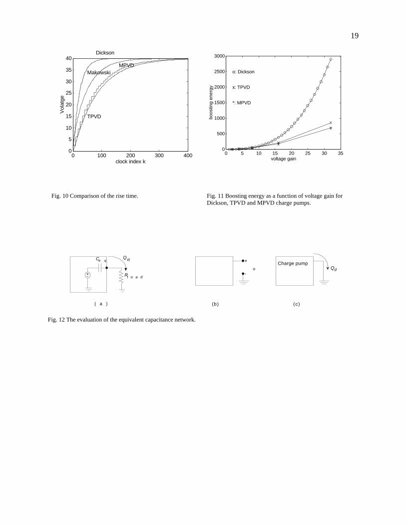
Fig. 11 Boosting energy as a function of voltage gain forDickson, TPVD and MPVD charge pumps.
Fig. 10 Comparison of the rise time.
0 5 10 15 20 25 30 350
500
1000
1500
2000
2500
3000
voltage gain
boos
ting
ener
gy
o: Dickson
x: TPVD
*: MPVD
0 100 200 300 4000
5
10
15
20
25
30
35
40
clock index k
Vol
atge
TPVD
Dickson
MakowskiMPVD
Rl o a d
QRCe q
( a )
+-
+
-o
Charge pumpQd
(b) (c)
Fig. 12 The evaluation of the equivalent capacitance network.
19
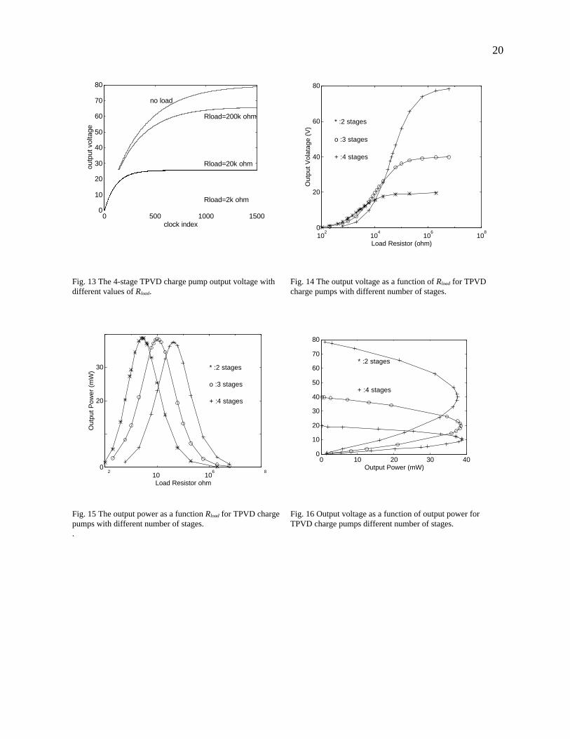
Fig. 14 The output voltage as a function of Rload for TPVDcharge pumps with different number of stages.
Fig. 13 The 4-stage TPVD charge pump output voltage withdifferent values of Rload.
102
104
106
108
0
20
40
60
80
Load Resistor (ohm)
Out
put V
olat
age
(V)
o :3 stages
+ :4 stages
* :2 stages
0 500 1000 15000
10
20
30
40
50
60
70
80
clock index
outp
ut v
olta
ge
Rload=2k ohm
Rload=20k ohm
Rload=200k ohm
no load
Fig. 16 Output voltage as a function of output power forTPVD charge pumps different number of stages.
Fig. 15 The output power as a function Rload for TPVD chargepumps with different number of stages..
0 10 20 30 400
10
20
30
40
50
60
70
80
Output Power (mW)
+ :4 stages
* :2 stages
210 10
6 80
20
30
Load Resistor ohm
Out
put P
ower
(m
W)
o :3 stages
+ :4 stages
* :2 stages
20
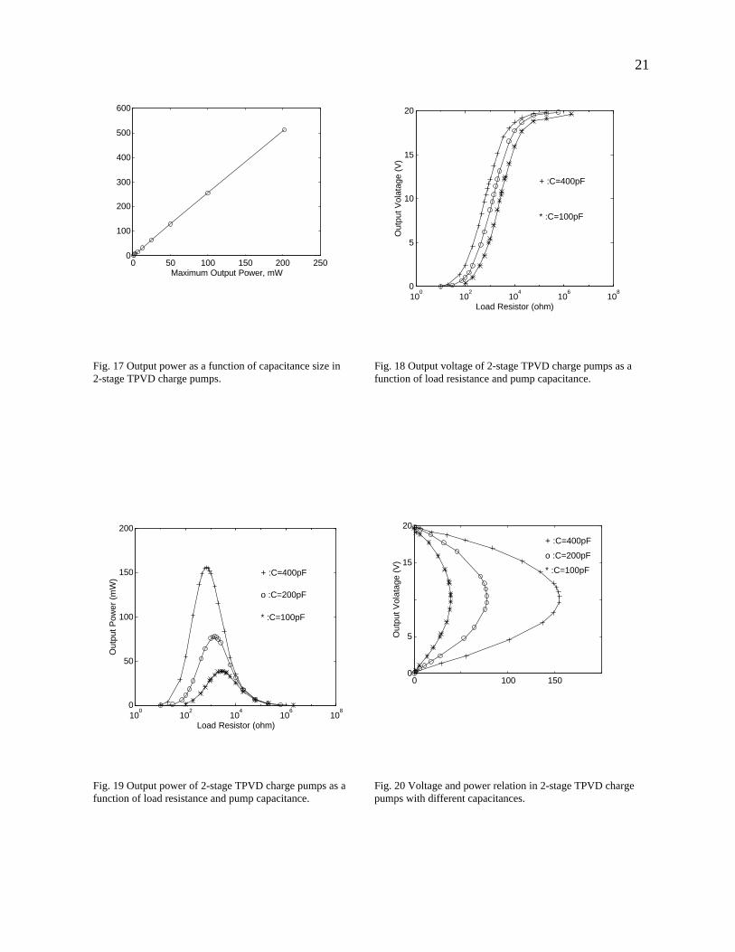
Fig. 18 Output voltage of 2-stage TPVD charge pumps as afunction of load resistance and pump capacitance.
Fig. 17 Output power as a function of capacitance size in2-stage TPVD charge pumps.
100
102
104
106
108
0
5
10
15
20
Load Resistor (ohm)
Out
put V
olat
age
(V)
+ :C=400pF
* :C=100pF
0 50 100 150 200 2500
100
200
300
400
500
600
Maximum Output Power, mW
Fig. 20 Voltage and power relation in 2-stage TPVD chargepumps with different capacitances.
Fig. 19 Output power of 2-stage TPVD charge pumps as afunction of load resistance and pump capacitance.
0 100 1500
5
15
20
Out
put V
olat
age
(V)
+ :C=400pF
o :C=200pF
* :C=100pF
100
102
104
106
108
0
50
100
150
200
Load Resistor (ohm)
Out
put P
ower
(m
W)
+ :C=400pF
o :C=200pF
* :C=100pF
21

Fig. 22 The output voltage as a function of RloadFig. 21 Changes in optimum load resistance and outputpower for different output voltage levels.
100 2
10 106 8
0
20
30
Load Resistor (ohm)
Out
put V
olat
age
(V)
x :MPVD
o :TPVD
+ :Makowski
* :Dickson
101
102
103
104
101
102
103
104
105
Max. power (mW)
* : Vout=20V
x : Vout=10V
Fig. 24 The Output voltage as function of the output power.Fig. 23 The output power as a function of Rload
0 100 150
5
10
20
25
35
40
Out
put V
olat
age
(V)
o :TPVD
x :MPVD
+ :Makowski
* :Dickson
100
102
104
106
108
0
50
100
150
Load Resistor ohm
Out
put P
ower
(m
W)
o :TPVD
x :MPVD
+ :Makowski
* :Dickson
22

2
1 2
1
CL
Vin
Cs
2
1 2
1
Cs2
1 CL2
Vout
2
1 2
1
CL
Cs
n
n1
Vout1 Vout2
n
Vin
21
Vin
21
Fig. 25 The modified TPVD charge pump.
Fig. 27 Rise time optimization of TPVD charge pump.Fig. 26 The output power of the original and the modified2-stage TPVD charge pump with equal capacitors.
0 20 40 60 800
5
10
15
rise time (micro sec)
volta
ge g
ain
1-stage
2-stage
3-stage
4-stage
100
102
104
106
108
0
20
40
60
80
Out
put P
ower
(m
W)
o :TPVD
x :modified TPVD
Load Resistor ohm
Fig. 29 Optimized boosting time as a function of desiredvoltage.
Fig. 28 Rise time optimization of fixed area designDickson charge pump.
0 5 10 15 200
10
20
30
40
50
60
70
80
desired voltage gain
rise
time
(mic
ro s
ec)
Makowski
MPVD
TPVD
0 10 20 30 400
5
10
15
20
rise time (micro sec)
volta
ge g
ain
23

Fig. 31 Fixed area design : output power as a function of theload resistance.
Fig. 30 Fixed area design: output voltage as a function of theload resistance.
100
102
104
106
0
50
100
150
200
250
Load Resistor (ohm)
Out
put P
ower
(m
Wat
t)
o :TPVD
x :MPVD
+ :Makowski
* :Dickson
100
102
104
106
0
10
20
30
40
Load Resistor (ohm)
Out
put V
olat
age
(V)
o :TPVD
x :MPVD
+ :Makowski
* :Dickson
24


![A High-Gain Cockcroft-Walton- Doubler-Based Switched ... · isolated high step-up DC-DC converter adopting switched- capacitor cell [14]. In order to increase the voltage gain, it](https://static.fdocuments.in/doc/165x107/5f5e7c0cd91e3b752c3d2ba9/a-high-gain-cockcroft-walton-doubler-based-switched-isolated-high-step-up-dc-dc.jpg)