
A CP GPS ANTENNA FROM 1.1 TO 1.6 GHZ · Project Number: MQP SNM - 2307 A CP GPS ANTENNA FROM 1.1 TO...
102
Project Number: MQP SNM - 2307 A CP GPS ANTENNA FROM 1.1 TO 1.6 GHZ A Major Qualifying Project Report Submitted to the Faculty of the WORCESTER POLYTECHNIC INSTITUTE In partial fulfillment of the requirements for the Degree of Bachelor of Science By: ______________________________ ______________________________ Jessica Nieves Garabed Hagopian April, 2008 APPROVED: ______________________________ Prof. Sergey Makarov, Advisor Electrical and Computer Engineering Department
Transcript of A CP GPS ANTENNA FROM 1.1 TO 1.6 GHZ · Project Number: MQP SNM - 2307 A CP GPS ANTENNA FROM 1.1 TO...
Project Number: MQP SNM - 2307
A CP GPS ANTENNA FROM 1.1 TO 1.6 GHZ
A Major Qualifying Project Report Submitted to the Faculty of the
WORCESTER POLYTECHNIC INSTITUTE
In partial fulfillment of the requirements for the
Degree of Bachelor of Science
By:
______________________________ ______________________________
Jessica Nieves Garabed Hagopian
April, 2008
APPROVED:
______________________________ Prof. Sergey Makarov, Advisor
Electrical and Computer Engineering Department

i
Table of Contents
ABSTRACT ................................................................................................................................................................. 1
ACKNOWLEDGMENTS ........................................................................................................................................... 2
EXECUTIVE SUMMARY ......................................................................................................................................... 3
INTRODUCTION ....................................................................................................................................................... 5
APPLICATIONS ........................................................................................................................................................... 6 REQUIREMENTS ......................................................................................................................................................... 7
PARTS .......................................................................................................................................................................... 8
HYBRIDS ................................................................................................................................................................... 8 90˚ Hybrid (Quadrature) ..................................................................................................................................... 9 180˚ Hybrids ........................................................................................................................................................ 9
BALUN .................................................................................................................................................................... 12 PRINTED CIRCUIT BOARD ........................................................................................................................................ 13 CHOKE RING ........................................................................................................................................................... 14
ANSOFT ..................................................................................................................................................................... 16
WHAT IS ANSOFT? ................................................................................................................................................... 17 ANTENNA SIMULATION ........................................................................................................................................... 17 OPTIMIZATION ......................................................................................................................................................... 19
ANTENNA ASSEMBLY .......................................................................................................................................... 21
PROCESS .................................................................................................................................................................. 21 Problems ............................................................................................................................................................ 22
TESTING ................................................................................................................................................................... 22
PROCESS .................................................................................................................................................................. 22 S11/22 Calibration Tests ....................................................................................................................................... 22 S21 Calibration Tests .......................................................................................................................................... 23
RESULTS .................................................................................................................................................................. 23
FIRST DESIGN CONCLUSIONS ........................................................................................................................... 27
NEW ANTENNA DESIGN ...................................................................................................................................... 29
PARTS ...................................................................................................................................................................... 29 Printed Circuit Board Design ............................................................................................................................ 29 Balun .................................................................................................................................................................. 31
ANTENNA FABRICATION ......................................................................................................................................... 32 Testing Results ................................................................................................................................................... 35
SECOND ANTENNA CONCLUSIONS ................................................................................................................. 42
APPENDIX A: DESIGN PARAMETERS .............................................................................................................. 45
APPENDIX B: MATLAB CODE ........................................................................................................................... 47
S11 CALIBRATION ..................................................................................................................................................... 47 S21 CALIBRATION .................................................................................................................................................... 49
APPENDIX C: TESTING RESULTS OF THE FIRST DESIGN ........................................................................ 51
PRIMARY TESTING RESULTS ................................................................................................................................... 51 Antenna 1 ........................................................................................................................................................... 51 Antenna 2 ........................................................................................................................................................... 54 Antenna 3 ........................................................................................................................................................... 57
RESULTS OF TESTING WITHOUT GROUND PLANE ..................................................................................................... 59

ii
Antenna 1 ........................................................................................................................................................... 59 Antenna 2 ........................................................................................................................................................... 62 Antenna 3 ........................................................................................................................................................... 65
IMPEDANCE TESTING ............................................................................................................................................... 68 Antenna 1 ........................................................................................................................................................... 68 Antenna 2 ........................................................................................................................................................... 70 Antenna 3 ........................................................................................................................................................... 72
HYBRIDS TAPED TO GROUND PLANE ...................................................................................................................... 74 Antenna 1 ........................................................................................................................................................... 74 Antenna 2 ........................................................................................................................................................... 76 Antenna 3 ........................................................................................................................................................... 78
APPENDIX D: TESTING RESULTS OF THE SECOND DESIGN ................................................................... 81
1.2 MM CENTER CONDUCTOR ANTENNAS ................................................................................................................ 81 Antenna 1 ........................................................................................................................................................... 81 Antenna 2 ........................................................................................................................................................... 85
2 MM CENTER CONDUCTOR ANTENNA .................................................................................................................... 89 3 MM CENTER CONDUCTOR ANTENNA .................................................................................................................... 92
REFERENCES .......................................................................................................................................................... 95

iii
Table of Figures Figure 1: An example of triangulation [1] ...................................................................................... 5
Figure 2: Four satellites are better than three [1] ............................................................................ 5
Figure 3: Base station in Summit Camp, Greenland [4] ................................................................. 7
Figure 4: Circular polarization [5] .................................................................................................. 8
Figure 5: Circuit Representation of a Branch Line Hybrid ............................................................ 9
Figure 6: Ring Hybrid in Microstrip Form .................................................................................. 10
Figure 7: Tapered Coupled Line Hybrid ...................................................................................... 10
Figure 8: Waveguide Hybrid Junction (magic-T) ......................................................................... 11
Figure 9: Classic Dyson balun for a) dipole antenna; b) – loop antenna. ..................................... 12
Figure 10: Dyson Balun Top view ................................................................................................ 13
Figure 11: PCB design done in PCB Artist .................................................................................. 14
Figure 12: 3D Simulation of PCB in Ansoft ................................................................................. 14
Figure 13: Choke ring and received waves ................................................................................... 15
Figure 14: Choke ring ................................................................................................................... 16
Figure 15: Top View ..................................................................................................................... 17
Figure 16: Side view ..................................................................................................................... 18
Figure 17: Angle view .................................................................................................................. 18
Figure 18: Simulated voltages using wave ports .......................................................................... 19
Figure 19: Results for SD11 from parameter sweep of both beta (degrees) and wing length (mm)....................................................................................................................................................... 20
Figure 20: Results for SD21 from parameter sweep of both beta (degrees) and wing length (mm)....................................................................................................................................................... 20
Figure 21: Results of differential equations using optimized values of beta and wing length ..... 21 Figure 22: Antenna 3 Return Loss ............................................................................................... 24
Figure 23: Antenna 3 S11 Impedance ........................................................................................... 24
Figure 24: Antenna 3 Isolation .................................................................................................... 25
Figure 25: Antenna 3 Return Loss without Ground plane .......................................................... 25
Figure 26: Antenna 3 Isolation without Ground plane ................................................................ 26
Figure 27: Antenna 3 Return Loss with Hybrids taped to Ground plane .................................... 26
Figure 28: Cross Sectional Balun Dimensions ............................................................................ 32
Figure 29: Teflon Block ............................................................................................................... 32
Figure 30: Completed Teflon Pyramid ........................................................................................ 33
Figure 31: Balun Jig ..................................................................................................................... 34
Figure 32: Completed Balun ........................................................................................................ 34
Figure 33: 1.2mm Center Conductor Antenna 1 S11 .................................................................... 35
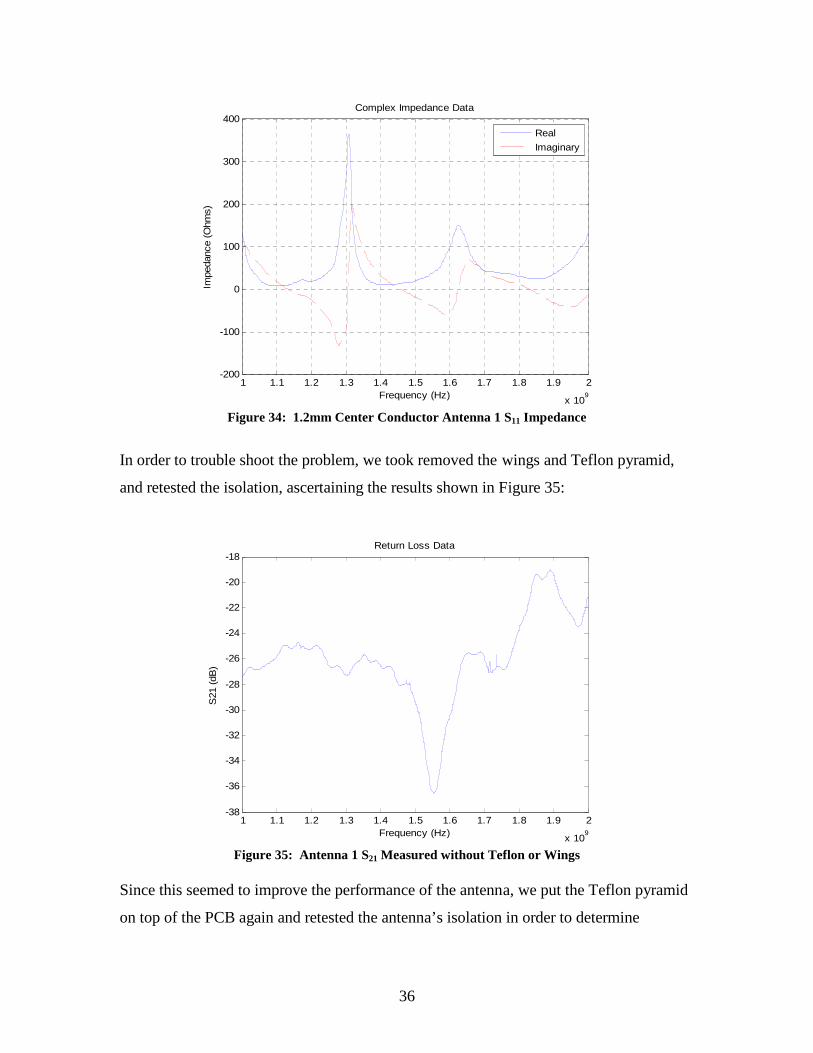
Figure 34: 1.2mm Center Conductor Antenna 1 S11 Impedance ................................................. 36
Figure 35: Antenna 1 S21 Measured without Teflon or Wings .................................................... 36
Figure 36: Antenna 1 S21 Measured with Teflon, without Wings ............................................... 37
Figure 37: 2 mm Antenna Balun Cross Section........................................................................... 38
Figure 38: 2 mm Antenna S11 ...................................................................................................... 38
Figure 39: 2 mm Antenna S22 ...................................................................................................... 39
Figure 40: 2 mm Antenna S21 ...................................................................................................... 39
Figure 41: 3 mm Antenna S11 ...................................................................................................... 40
Figure 42: 3 mm Antenna S22 ...................................................................................................... 41
Figure 43: 3 mm Antenna S21 ...................................................................................................... 41

iv
Figure 44: 3 mm Antenna S11 with 90° hybrid ............................................................................ 42
Figure 45: Final Design Top View .............................................................................................. 43
Figure 46: Final Design Bottom View ......................................................................................... 43
Figure 47: Final Design Side View .............................................................................................. 44
Figure 48: Design parameters for first design............................................................................... 45
Figure 49: Design parameters for second design .......................................................................... 46
Figure 50: First Antenna 1 S11 ..................................................................................................... 51
Figure 51: First Antenna 1 S11 Impedance ................................................................................... 51
Figure 52: Second Antenna 1 S11 ................................................................................................. 52
Figure 53: Second Antenna 1 S11 Impedance .............................................................................. 52
Figure 54: Antenna 1 S21.............................................................................................................. 53
Figure 55: Antenna 1 S21 Calibration Impedance Results ........................................................... 53
Figure 56: Antenna 1 S11 Measured by Network Analyzer ......................................................... 54
Figure 57: Antenna 1 S21 Measured by Network Analyzer ......................................................... 54
Figure 58: Antenna 2 S11.............................................................................................................. 55
Figure 59: Antenna 2 S11 Impedance ........................................................................................... 55
Figure 60: Antenna 2 S21.............................................................................................................. 56
Figure 61: Antenna 2 S21 Impedance ........................................................................................... 56
Figure 62: Antenna S21 Measured by Network Analyzer ............................................................ 57
Figure 63: Antenna 3 S11.............................................................................................................. 57
Figure 64: Antenna 3 S11 Impedance ........................................................................................... 58
Figure 65: Antenna 3 S21.............................................................................................................. 58
Figure 66: Antenna 3 S21 Impedance ........................................................................................... 59
Figure 67: Antenna 1 S11 without Ground plane ......................................................................... 59
Figure 68: Antenna 1 S11 Impedance without Ground plane ....................................................... 60
Figure 69: Antenna 1 S22 without Ground plane ......................................................................... 60
Figure 70: Antenna 1 S22 Impedance without Ground plane ....................................................... 61
Figure 71: Antenna 1 S21 without Ground plane ......................................................................... 61
Figure 72: Antenna 1 S21 Impedance without Ground plane ....................................................... 62
Figure 73: Antenna 2 S11 without Ground plane ......................................................................... 62
Figure 74: Antenna 2 S11 Impedance ........................................................................................... 63
Figure 75: Antenna 2 S22 without Ground plane ......................................................................... 63
Figure 76: Antenna 2 S22 Impedance without Ground plane ....................................................... 64
Figure 77: Antenna 2 S21 without Ground plane ......................................................................... 64
Figure 78: Antenna 2 S21 Impedance without Ground plane ....................................................... 65
Figure 79: Antenna 3 S11 without Ground plane ......................................................................... 65
Figure 80: Antenna 3 S11 Impedance without Ground plane ....................................................... 66
Figure 81: Antenna 3 S22 without Ground plane ......................................................................... 66
Figure 82: Antenna 3 S22 Impedance without Ground plane ....................................................... 67
Figure 83: Antenna 3 S21 without Ground plane ......................................................................... 67
Figure 84: Antenna 3 S21 Impedance without Ground plane ....................................................... 68
Figure 85: Antenna 1 Port 1 Impedance ...................................................................................... 68
Figure 86: Antenna 1 Port 2 Impedance ....................................................................................... 69
Figure 87: Antenna 1 Port 3 Impedance ....................................................................................... 69
Figure 88: Antenna 1 Port 4 Impedance ....................................................................................... 70
Figure 89: Antenna 2 Port 1 Impedance ....................................................................................... 70
Figure 90: Antenna 2 Port 2 Impedance ....................................................................................... 71
Figure 91: Antenna 2 Port 3 Impedance ....................................................................................... 71
Figure 92: Antenna 2 Port 4 Impedance ....................................................................................... 72

v
Figure 93: Antenna 3 Port 1 Impedance ....................................................................................... 72
Figure 94: Antenna 3 Port 2 Impedance ....................................................................................... 73
Figure 95: Antenna 3 Port 3 Impedance ....................................................................................... 73
Figure 96: Antenna 3 Port 4 Impedance ....................................................................................... 74
Figure 97: Antenna 1 S11 with Hybrids Taped to Ground plane.................................................. 74
Figure 98: Antenna 1 S11 Impedance with Hybrids Taped to Ground plane ............................... 75
Figure 99: Antenna 1 S22 with Hybrids Taped to Ground plane.................................................. 75
Figure 100: Antenna 1 S22 Impedance with Hybrids Taped to Ground plane ............................. 76
Figure 101: Antenna 2 S11 with Hybrids Taped to Ground plane ................................................ 76
Figure 102: Antenna 2 S11 Impedance with Hybrids Taped to Ground plane ............................. 77
Figure 103: Antenna 2 S22 Impedance with Hybrids Taped to Ground plane ............................. 77
Figure 104: Antenna 2 S22 Impedance with Hybrids Taped to Ground plane ............................. 78
Figure 105: Antenna 3 S11 with Hybrids Taped to Ground plane ................................................ 78
Figure 106: Antenna 3 S11 Impedance with Hybrids Taped to Ground plane ............................. 79
Figure 107: Antenna 3 S22 with Hybrids Taped to Ground plane ................................................ 79
Figure 108: Antenna 3 S22 Impedance with Hybrids Taped to Ground plane ............................. 80
Figure 109: 1.2mm Center Conductor Antenna 1 S11 .................................................................. 81
Figure 110: 1.2mm Center Conductor Antenna 1 S11 Impedance ............................................... 81
Figure 111: 1.2mm Center Conductor Antenna 1 S22 .................................................................. 82
Figure 112: 1.2mm Center Conductor Antenna 1 S22 Impedance ............................................... 82
Figure 113: 1.2mm Center Conductor Antenna 1 S21 .................................................................. 83
Figure 114: 1.2mm Center Conductor Antenna 1 S21 Impedance ............................................... 83
Figure 115: Antenna 1 S21 Measured without Teflon or Wings .................................................. 84
Figure 116: Antenna 1 S21 Impedance Measured without Teflon or Wings................................ 84
Figure 117: Antenna 1 S21 Measured with Teflon, without Wings ............................................. 85
Figure 118: Antenna 1 S21 Impedance Measured with Teflon, without Wings ........................... 85
Figure 119: Antenna 2 S21 Measured without Teflon or Wings .................................................. 86
Figure 120: Antenna 2 S21 Impedance Measured without Teflon or Wings................................ 86
Figure 121: First Trial Antenna 2 S21 Measured with Teflon, without Wings ............................ 87
Figure 122: First Trial Antenna 2 S21 Impedance Measured with Teflon, without Wings .......... 87
Figure 123: Second Trial Antenna 2 S21 Measured with Teflon, without Wings ........................ 88
Figure 124: Second Trial Antenna 2 S21 Impedance Measured with Teflon, without Wings ..... 88
Figure 125: 2 mm Center Conductor Antenna S21 Measured with no Teflon or Wings ............ 89
Figure 126: 2 mm Center Conductor Antenna S21 Impedance Measured with no Teflon or Wings....................................................................................................................................................... 89
Figure 127: 2 mm Center Conductor Antenna S11 ....................................................................... 90
Figure 128: 2 mm Center Conductor Antenna S11 Impedance .................................................... 90
Figure 129: 2 mm Center Conductor Antenna S22 ....................................................................... 91
Figure 130: 2 mm Center Conductor Antenna S22 Impedance .................................................... 91
Figure 131: 2 mm Center Conductor Antenna S21 ....................................................................... 92
Figure 132: 2 mm Center Conductor Antenna S21 Impedance .................................................... 92
Figure 133: 3 mm Center Conductor Antenna S11 ....................................................................... 93
Figure 134: 3 mm Center Conductor Antenna S22 ....................................................................... 93
Figure 135: 3 mm Center Conductor Antenna S21 ....................................................................... 94
Figure 136: 3 mm Center Conductor Antenna S11 with 90º Hybrid ............................................ 94

vi
Table of Tables
Table 1: Hybrid 1 Test Results .................................................................................................... 11
Table 2: Hybrid 2 Test Results .................................................................................................... 11
Table 3: Differential Variables .................................................................................................... 19
Table 4: Optimization Results ..................................................................................................... 20

1
Abstract
The aim of the project is to design a circularly polarized antenna for permanent GPS base
station applications with low return loss, high isolation, and a bandwidth of 1.1 to 1.6
GHz. The antenna was designed, built, and tested.

2
Acknowledgments
We would like to acknowledge Professor Sergey Makarov for all the help, insight, and
direction he gave to this project.
We would also like to recognize Mr. Eduardo Oliveira for the use of his MATLAB
calibration testing code as well as the multitude of answers he provided to any question
we had.
We would like to especially thank Mr. Patrick Morrison for the tireless effort he gave to
this project. His patience in showing us the many uses of each machine in the ECE shop
is much appreciated.
Lastly, we would like to thank Dr. Francesca Scappuzzo and Physical Sciences Inc. for
sponsoring our project.
Every one of these people was crucial to the completion of this project.
3
Executive Summary
Global Positioning System (GPS) was developed by the U.S. Department of Defense
because of the need of a precise positioning system. This worldwide radio navigation
system consists of 24 satellites and ground stations. GPS utilizes the L-band which is
roughly 1-2 GHz and can be further broken down into smaller bands L1-L5. The most
common and well known form of GPS is the navigation systems found in vehicles (TOM
TOM, Garmin etc.), boats and planes which are becoming more and more common;
however there are many other uses for GPS. For instance, GPS is being used in science
for the observation of volcanic activity and observation of weather affects on building
structures.
Our antenna should work in the L band so the frequency range will be 1.1-1.6 GHz.
Within this frequency range there should be good isolation which means it should have
minimal crosstalk between ports and low return loss or low power ratio (PR / PT). The
antenna should also have circular polarization. Before anything could be built, the
concept of the antenna had to be designed and simulated. Piece by piece the antenna was
created in a 3D software called Ansoft HFSS 10. This section describes the software
used, the simulation process and how Ansoft was used to optimize the measurements for
our antenna.
After ordering parts, the first step was to construct the wings out of brass. Initially, we
created wings 28 mm in length because our simulations early on in the project had shown
that was the best wing length. After further optimization simulations, it was decided that
the best combination of wing length and droop angle was 20.5 mm and 50 degrees
(respectively). We used the band saw to cut the brass and the belt sander to adjust the
dimensions on a finer scale. Afterwards, we use a file to smooth out the cuts and give the
wings a better appearance.
Next, we created the foundation for the antenna. After receiving 63 mm sections of a 0.5
inch (diameter) Teflon rod, we used the lathe to drill out the inside. We slowly worked
4
up to a diameter that could house the four coaxial cables inside the tube. Since the
printed circuit board (PCB) vias were still outside of that diameter, we expanded the
circle for about 1 cm into the end of the tube where the PCB would be in contact. Once
the antenna was built, we could proceed to test it.
The result did not turn out as we had expected. The most disconcerting characteristic
about the poor performance of the antennas is the fact that the results differed so greatly
from the Ansoft simulation results. This could have been caused by one a few different
variations from the simulated design. For instance, the simulated design contained an
electrically conductive sheet that connected the center conductors of the coaxial cables to
the wings.
The previous design did not meet requirements. For our new design we will continue to
use the Dyson balun but instead of coaxial cables we will use a quad line. Some
modifications will need to be made to accommodate this change. The following section
describes the modified parts and design for the new antenna.
The 1.2 mm antenna’s results were similar to the results of our first design. Increasing
the size of the center conductor seemed to drastically improve the performance of the
antenna. The quad line antenna with the 3 mm by 3 mm center conductor is a very good
design. In addition to the good results, the design is very sturdy, and is easily fixed to a
choke ring ground plane. Also, the antennas can easily be replicated, since the Teflon
pyramid, brass wings, printed circuit board, and coaxial cable connectors can be
accurately recreated in large numbers. The balun would be the only part requiring
creativity, since the jig that we used for the 1.2 mm center conductor balun was too small
for the 3 mm center conductor balun. For these reasons, we needed to use clamps to
hold the mircrostrip lines to the center conductor as well as a great deal of patience.
5
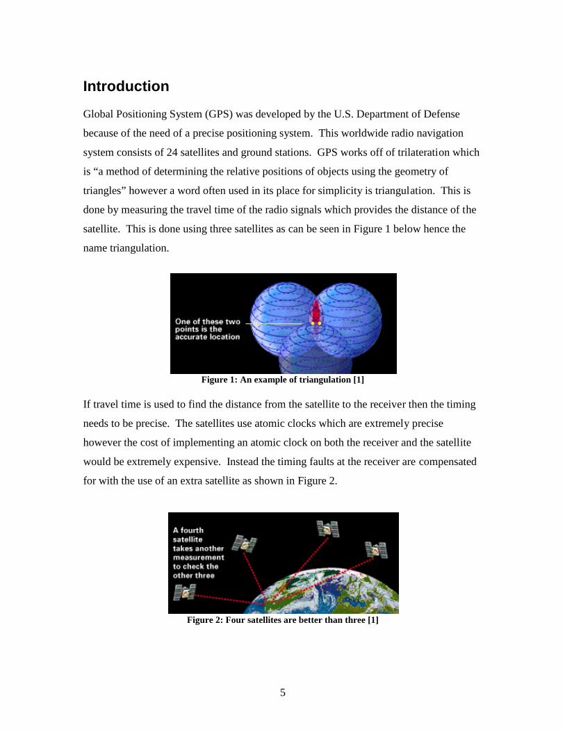
Introduction
Global Positioning System (GPS) was developed by the U.S. Department of Defense
because of the need of a precise positioning system. This worldwide radio navigation
system consists of 24 satellites and ground stations. GPS works off of trilateration which
is “a method of determining the relative positions of objects using the geometry of
triangles” however a word often used in its place for simplicity is triangulation. This is
done by measuring the travel time of the radio signals which provides the distance of the
satellite. This is done using three satellites as can be seen in Figure 1 below hence the
name triangulation.
Figure 1: An example of triangulation [1]
If travel time is used to find the distance from the satellite to the receiver then the timing
needs to be precise. The satellites use atomic clocks which are extremely precise
however the cost of implementing an atomic clock on both the receiver and the satellite
would be extremely expensive. Instead the timing faults at the receiver are compensated
for with the use of an extra satellite as shown in Figure 2.
Figure 2: Four satellites are better than three [1]

6
All GPS receivers have an almanac programmed into their computers that informs them
where each satellite is at all times. The charged particles located in the ionosphere and
the water vapor of the troposphere also create timing errors as the signals move through
them. Once the signal is closer buildings, tunnels, trees etc. can also cause an error that is
referred to as multipath.
GPS utilizes the L-band which is roughly 1-2 GHz and can be further broken down into
smaller bands L1-L5. The L1 band is centered at 1575.42 MHz and is used for coarse-
acquisition (C/A) code and encrypted precision P(Y) code. The L2 band is centered at
1227.60 MHz and is used for P(Y) code. The L3 band is centered at 1381.05 MHz and is
used to enforce nuclear test ban treaties. The L4 band is centered at 1379.913 MHz and
is currently being studied for additional correction in the ionosphere. The L5 band is
centered at 1176.45 MHz and is used as an internationally protected range for
aeronautical navigation, which has little to no interference under any circumstances.
Applications The most common and well known form of GPS is the navigation systems found in
vehicles (TOM TOM, Garmin etc.), boats and planes which are becoming more and more
common; however there are many other uses for GPS. Tracking has become easier with
the use of GPS. This can be seen in the Precision Personnel Locator project which is a
project developed “to help protect the lives of emergency personnel through a system for
indoor personnel location and tracking” [2]. An Inertially augmented GPS landing
system is being developed by Leonard R. Anderson and Melville D. McIntyr which also
utilizes tracking.
“The guidance software may be executed by a conventional airplane
processor, such as the GPS landing system processor, the internal
reference system processor or the airplane's autopilot processor, or by a
separate stand-alone processor. The runway centerline information is
stored at the ground station or in local memory. The ground station can
also provide differential GPS information.” [3]
7
This means that the there is a stationary receiver that has the runway information stored
and the plane is able to communicate with the ground station to make landing easier and
safer. The military utilizes GPS in the form of missile guidance and search and rescue
missions. GPS is also being used in science for the observation of volcanic activity and
observation of weather affects on building structures. For these scientific observations
permanent base stations are used. Like the name implies, these antennas are permanently
placed in a location to provide high precision accuracy. UNAVCO is a company that
specializes in such antennas and base stations. More specifically their “survey systems
provide real-time kinematic (RTK) broadcasts for centimeter level differential corrections
to properly equipped users, simplifying many GPS survey tasks that would otherwise
require time consuming collection and post-processing of data. The equipment may also
be used for post-processed static and kinematic surveys.” [4] Below in Figure 3 is a base
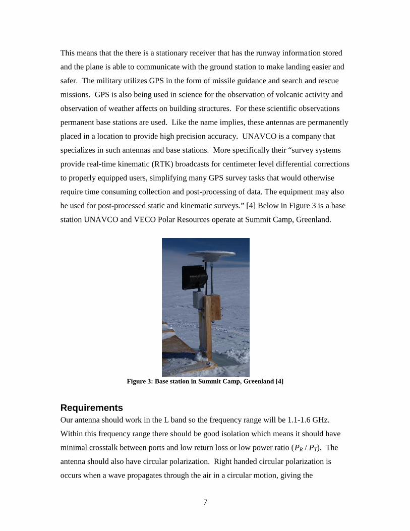
station UNAVCO and VECO Polar Resources operate at Summit Camp, Greenland.
Figure 3: Base station in Summit Camp, Greenland [4]
Requirements Our antenna should work in the L band so the frequency range will be 1.1-1.6 GHz.
Within this frequency range there should be good isolation which means it should have
minimal crosstalk between ports and low return loss or low power ratio (PR / PT). The
antenna should also have circular polarization. Right handed circular polarization is
occurs when a wave propagates through the air in a circular motion, giving the

8
appearance of a spiral. It is created when two dipoles are exactly 90 degrees out of
phase. Right handed circular polarization is crucial to GPS antennas, since it allows for
received signals from any direction. A linearly polarized signal will not be received by a
dipole antenna if the antenna does not exactly line up with the signal. A circularly
polarized will always line up with a turnstile antenna.
Figure 4: Circular polarization [5]
Parts
In the following section the parts needed for the assembly of our antenna will be
described in detail along with why they were chosen.
Hybrids
90˚ and 180˚ hybrids are passive circuits used for higher frequency applications. They
are classified as power dividers and directional couples, and are used for power division
and combination (respectively). These hybrids are often connected to an antenna in order
to create circle polarization. Circle polarization is necessary for all antennas that are not
fixed in one spot.

90˚ Hybrid (Quadrature)
The 90 hybrid is a four port network with one input port, two output ports, and one
isolated port. When a voltage signal is sent through the input port, there a 90
difference will appear on the output ports. A circuit representation
show in Figure 5:
Figure 5: Circuit Representation of a Branch Line Hybrid
As can be seen from Figure 5, the branch line hybrid is symmetrical. This causes the S
parameters to also be symmetrical. The scattering matrix for a branch line hybrid is
shown in Equation 1:
180˚ Hybrids
180 hybrids are also four port networks with one input port (port 1), two output ports
(ports 2 and 3), and one isolated port (port 4). When a voltage signal is sent into the port
1 input, a phase difference of 0˚ w
isolated. However, when a voltage signal is sent into port 4, an 180
will appear across ports 2 and 3, while port 1 will be isolated. In both cases, the
components of voltage signal that appear at ports 2 and 3 will be equal in magnitude.
9
˚ hybrid is a four port network with one input port, two output ports, and one
isolated port. When a voltage signal is sent through the input port, there a 90˚ phase
difference will appear on the output ports. A circuit representation a branch line hybrid is
: Circuit Representation of a Branch Line Hybrid
, the branch line hybrid is symmetrical. This causes the S
parameters to also be symmetrical. The scattering matrix for a branch line hybrid is
−=
010
001
100
010
2
1][
j
j
j
j
S
˚ hybrids are also four port networks with one input port (port 1), two output ports
(ports 2 and 3), and one isolated port (port 4). When a voltage signal is sent into the port
˚ will appear across ports 2 and 3, while port 4 will be
isolated. However, when a voltage signal is sent into port 4, an 180 phase difference
will appear across ports 2 and 3, while port 1 will be isolated. In both cases, the
that appear at ports 2 and 3 will be equal in magnitude.
˚ hybrid is a four port network with one input port, two output ports, and one
˚ phase
a branch line hybrid is
, the branch line hybrid is symmetrical. This causes the S-
parameters to also be symmetrical. The scattering matrix for a branch line hybrid is
(1)
˚ hybrids are also four port networks with one input port (port 1), two output ports
(ports 2 and 3), and one isolated port (port 4). When a voltage signal is sent into the port
ill appear across ports 2 and 3, while port 4 will be
˚ phase difference
that appear at ports 2 and 3 will be equal in magnitude.

When an 180 hybrid is used as a coupler, voltage signals are sent into the output ports
(ports 2 and 3). When this happens, the sum of the signals will appear at port 1, while the
difference of the two signals will appear at port 4. The scattering matrix for an 180
hybrid is shown in Equation 2:
It should be noted that the scattering matrix for the 180
symmetric. Three common 180˚ hybrid
Figure 6
Figure
10
˚ hybrid is used as a coupler, voltage signals are sent into the output ports
(ports 2 and 3). When this happens, the sum of the signals will appear at port 1, while the
e two signals will appear at port 4. The scattering matrix for an 180
−
−−=
0110
1001
1001
0110
2][
jS
It should be noted that the scattering matrix for the 180 hybrid is both unitary and
˚ hybrids are shown below:
6: Ring Hybrid in Microstrip Form
Figure 7: Tapered Coupled Line Hybrid
˚ hybrid is used as a coupler, voltage signals are sent into the output ports
(ports 2 and 3). When this happens, the sum of the signals will appear at port 1, while the
e two signals will appear at port 4. The scattering matrix for an 180
(2)
˚ hybrid is both unitary and

Figure 8: Waveguide Hybrid Junction (magic Since these antennas were created for GPS applications, we needed to create circular
polarization. For this reason, we decided to use two 180º hybrids. After careful research,
we decided to order the two hybrids from Mini
specified bandwidth of 1000 to 2000 MHz, since our antennas need to operate in the L
Band. Table 1 and Table 2 show the results for the preliminary testing on the two
hybrids.
S12, dB S21, dB
power
(dB)
frequency
(GHz)
power
(dB)
max -31.3 1.10 -31.4
min -42.8 1.43 -42.8
Table
S12, dB S21, dB
power
(dB)
frequency
(GHz)
power
(dB)
max -30.9 1.10 -30.9
min -43.6 1.44 -43.5
Table
Both of these hybrids are very broadband, with a very flat
also showed good isolation, with cross talk values below 40 dB.
11
: Waveguide Hybrid Junction (magic-T)
Since these antennas were created for GPS applications, we needed to create circular
polarization. For this reason, we decided to use two 180º hybrids. After careful research,
we decided to order the two hybrids from Mini-Circuits. We selected hybrids that had a
specified bandwidth of 1000 to 2000 MHz, since our antennas need to operate in the L
show the results for the preliminary testing on the two
S21, dB Ss1, dB Ss2. DB
power frequency
(GHz)
power
(dB)
Frequency
(GHz)
power
(dB)
frequency
(GHz)
31.4 1.10 -4.4 1.16 -4.67 1.10
42.8 1.43 -48 1.44 -4.95 1.44
Table 1: Hybrid 1 Test Results
S21, dB Ss1, dB Ss2, dB
power frequency
(GHz)
power
(dB)
Frequency
(GHz)
power
(dB)
frequency
(GHz)
30.9 1.10 -4.9 1.60 -4.9 1.60
43.5 1.44 -4.6 1.10 -4.6 1.10
Table 2: Hybrid 2 Test Results
Both of these hybrids are very broadband, with a very flat linear response. The hybrids
also showed good isolation, with cross talk values below 40 dB.
Since these antennas were created for GPS applications, we needed to create circular
polarization. For this reason, we decided to use two 180º hybrids. After careful research,
hat had a
specified bandwidth of 1000 to 2000 MHz, since our antennas need to operate in the L
show the results for the preliminary testing on the two
Ss2. DB
frequency
(GHz)
1.10
1.44
Ss2, dB
frequency
(GHz)
1.60
1.10
linear response. The hybrids

12
Balun
The term balun is an abbreviation of the words balance and unbalance. It is a device that
connects a balanced two-conductor line to an unbalanced coaxial line. We selected the
Dyson balun for our antenna. Its concept is shown in Figure 5 that follows.
Figure 9: Classic Dyson balun for a) dipole antenna; b) – loop antenna.
Either wing of the dipole in Fig. 5a is fed with a separate coaxial line, sharing the same
outer ground; both lines are 180 deg out of phase. This ensures the proper balanced
current distribution along the dipole. A similar setup can also be applied to a loop antenna
– see Figure 5b. The proper power division and the proper phase shift can be obtained
by the use of a 180 deg standard hybrid shown in Figure 5. The hybrid is thus playing the
role of a balun; the ground is the case of the hybrid. Electric current on both lines feeding
the dipole can be considered having ±90 deg phase shift versus ground reference with no
current.
13
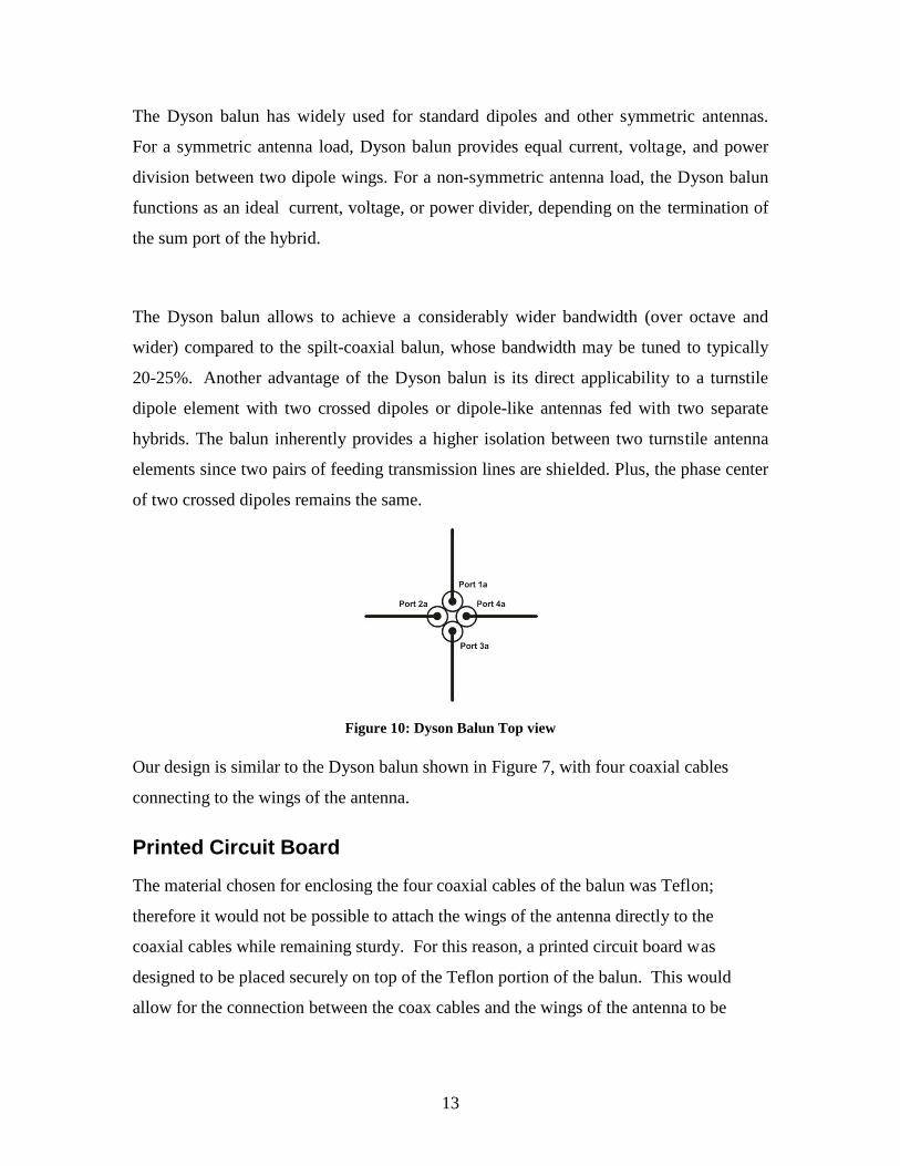
The Dyson balun has widely used for standard dipoles and other symmetric antennas.
For a symmetric antenna load, Dyson balun provides equal current, voltage, and power
division between two dipole wings. For a non-symmetric antenna load, the Dyson balun
functions as an ideal current, voltage, or power divider, depending on the termination of
the sum port of the hybrid.
The Dyson balun allows to achieve a considerably wider bandwidth (over octave and
wider) compared to the spilt-coaxial balun, whose bandwidth may be tuned to typically
20-25%. Another advantage of the Dyson balun is its direct applicability to a turnstile
dipole element with two crossed dipoles or dipole-like antennas fed with two separate
hybrids. The balun inherently provides a higher isolation between two turnstile antenna
elements since two pairs of feeding transmission lines are shielded. Plus, the phase center
of two crossed dipoles remains the same.
Figure 10: Dyson Balun Top view Our design is similar to the Dyson balun shown in Figure 7, with four coaxial cables
connecting to the wings of the antenna.
Printed Circuit Board
The material chosen for enclosing the four coaxial cables of the balun was Teflon;
therefore it would not be possible to attach the wings of the antenna directly to the
coaxial cables while remaining sturdy. For this reason, a printed circuit board was
designed to be placed securely on top of the Teflon portion of the balun. This would
allow for the connection between the coax cables and the wings of the antenna to be

14
made and remain sturdy. After designing several layouts for the PCB in a program called
PCB Artist, we decided on the preliminary design shown in Figure 11 below:
Figure 11: PCB design done in PCB Artist
The diagonal length of the board was designed to be ½ inches so that the PCB is able to
sit properly on the balun with no protruding edges. The vias were designed to be the 40
mils so that the inner conductors of the coaxial cables were able to fit through with ease.
The copper pads were laid out in such a way so that the area of each pad could be
increased to the desired size while keeping the sides of the board symmetrical. The board
design was then sent to Advanced Circuits to be printed.
Figure 12: 3D Simulation of PCB in Ansoft
Choke Ring
A choke ring ground plane consists of several concentric thin rings around the center
where the antenna is located. The areas between the rings are referred to as "grooves".
The signal that is received by the antenna is composed of two components. There is a
"direct" signal, which is the signal we want, and a "reflected" signal, which is the
unwanted, signal that could be waves reflected off of buildings, trees, etc.

15
Figure 13: Choke ring and received waves
The electromagnetic field of the reflected signal in the vicinity of the choke ring ground
plane can be viewed as sum of two field waves. The first of the two, primary waves,
move around the perimeter of the ground plane never entering the grooves, as shown in
Figure 10. This behavior is similar to how a reflected wave would act on a flat ground
plane. The second of the two, secondary waves, are reflected waves created by the
electromagnetic field of the grooves.
Primary and secondary reflected signals propagate to the antenna element and contribute
to the total signal that also includes direct signal from the satellite to the antenna. The
objective of the choke ring ground plane is for the primary and secondary reflected
signals to cancel each other out and have the direct signal remain the dominant signal.
The phase relationship between the primary and the secondary reflected signals at the
antenna output depends on the difference in path lengths that each signal travels. This
path difference is twice the depth of the grooves. The amplitude ratio of the two signals
depends on the characteristics of the antenna element, its location on the ground plane,
the width and the number of the grooves. If the amplitude of the primary and the
secondary waves are equal in magnitude and the phase between them is 180 degrees, then
the two waves cancel each other out and multi-path is suppressed, allowing for the
objective of the choke ring to be obtained, making the direct signal the dominant signal.
“For a given choke ring ground plane the complete suppression of multi-
path only occurs for certain elevation angles and for others the multi-path
is partially suppressed. The maximum suppression usually occurs for the
16
angles close to zenith and minimal suppression at angles close to horizon.”
[6]
Therefore it acts as a kind of band pass filter only allowing waves to reach that are within
a given angle.
Studies have concluded that the depth of the grooves should be close to the quarter of the
wavelength but slightly more to avoid creation of another surface wave component which
destroys the required phase and amplitude ratios between the primary and the secondary
waves. [6]
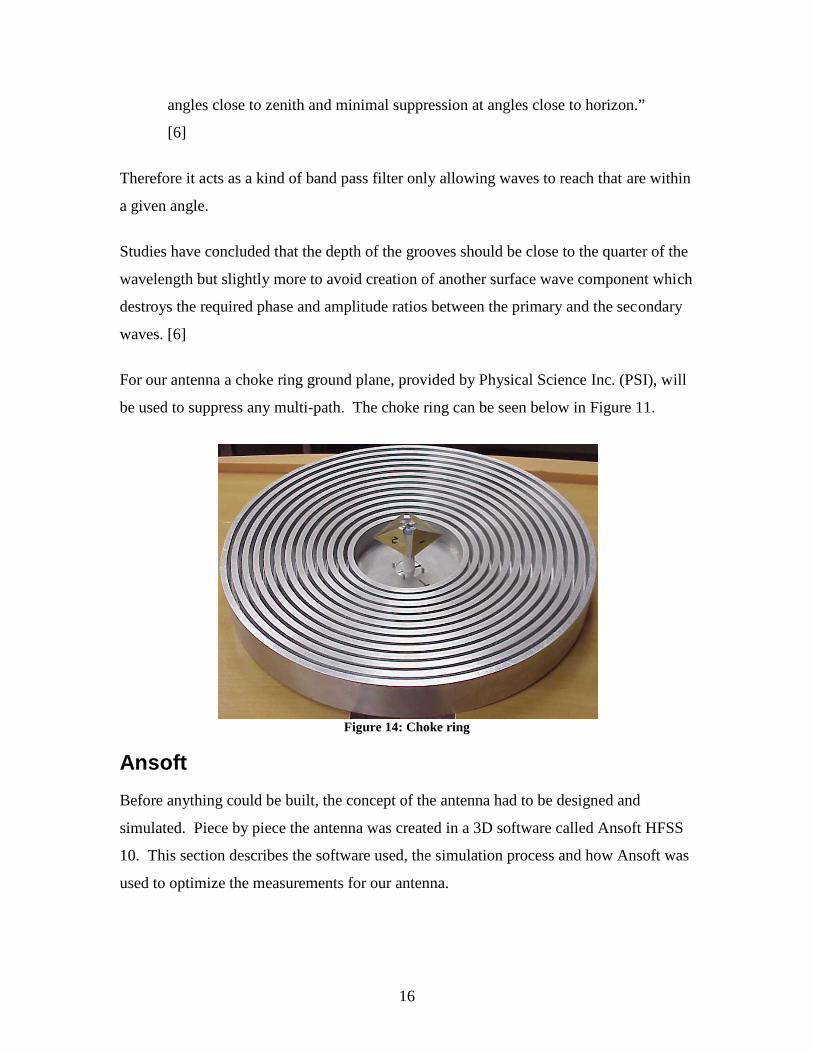
For our antenna a choke ring ground plane, provided by Physical Science Inc. (PSI), will
be used to suppress any multi-path. The choke ring can be seen below in Figure 11.
Figure 14: Choke ring
Ansoft
Before anything could be built, the concept of the antenna had to be designed and
simulated. Piece by piece the antenna was created in a 3D software called Ansoft HFSS
10. This section describes the software used, the simulation process and how Ansoft was
used to optimize the measurements for our antenna.
17
What is Ansoft?
“Ansoft HFSS is an interactive software package for calculating the electromagnetic
behavior of a structure. The software includes post-processing commands for analyzing
this behavior in detail. In using HFSS, you can compute:
• Basic electromagnetic field quantities and, for open boundary problems, radiated near
and far fields.
• Characteristic port impedances and propagation constants.
• Generalized S-parameters and S-parameters renormalized to specific port impedances.
• The eigen modes, or resonances, of a structure.” [7]
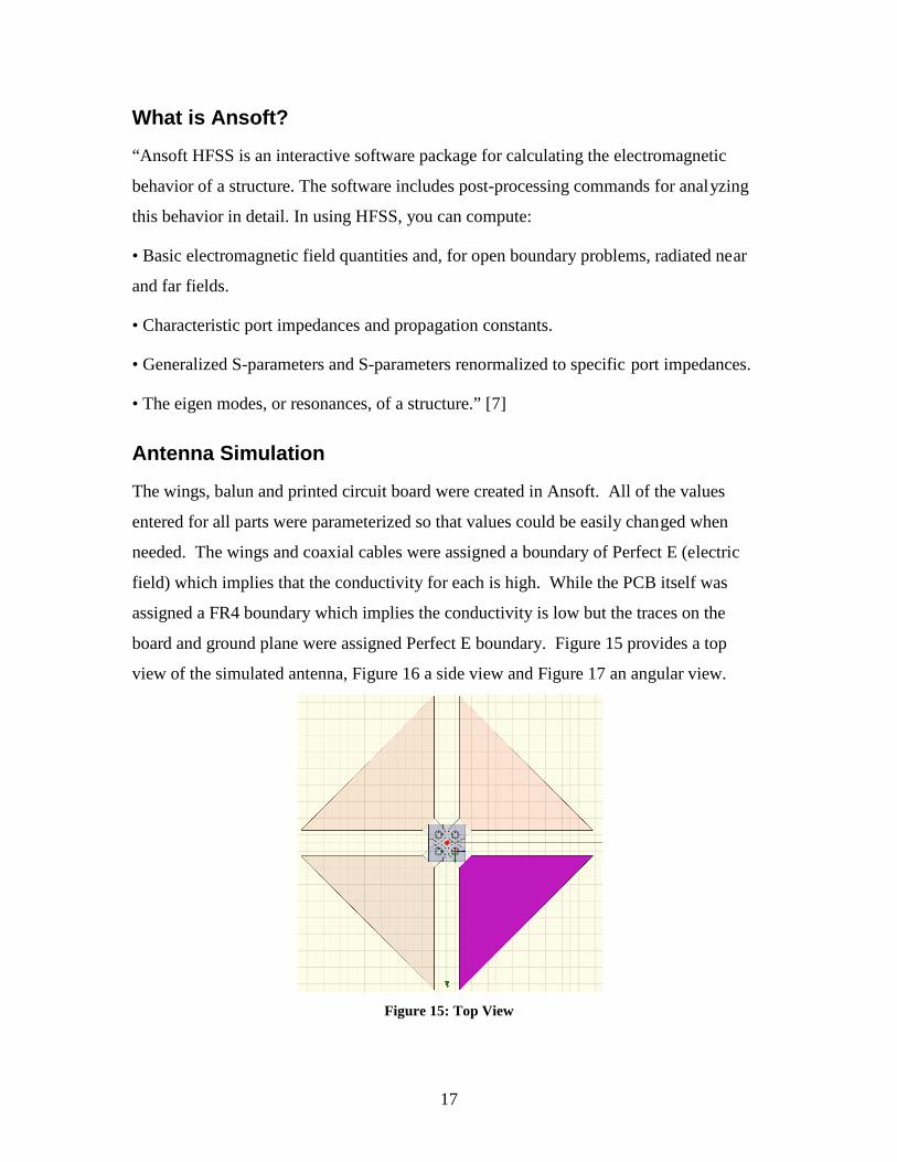
Antenna Simulation
The wings, balun and printed circuit board were created in Ansoft. All of the values
entered for all parts were parameterized so that values could be easily changed when
needed. The wings and coaxial cables were assigned a boundary of Perfect E (electric
field) which implies that the conductivity for each is high. While the PCB itself was
assigned a FR4 boundary which implies the conductivity is low but the traces on the
board and ground plane were assigned Perfect E boundary. Figure 15 provides a top
view of the simulated antenna, Figure 16 a side view and Figure 17 an angular view.
Figure 15: Top View

18
Figure 16: Side view
Figure 17: Angle view
19
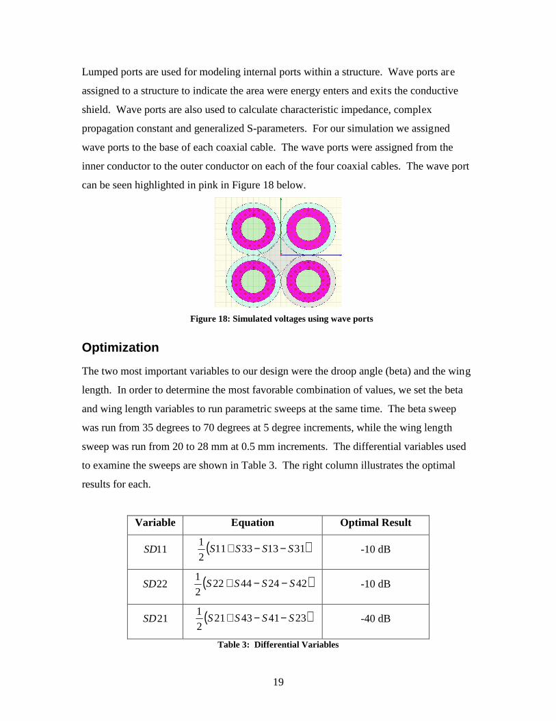
Lumped ports are used for modeling internal ports within a structure. Wave ports are
assigned to a structure to indicate the area were energy enters and exits the conductive
shield. Wave ports are also used to calculate characteristic impedance, complex
propagation constant and generalized S-parameters. For our simulation we assigned
wave ports to the base of each coaxial cable. The wave ports were assigned from the
inner conductor to the outer conductor on each of the four coaxial cables. The wave port
can be seen highlighted in pink in Figure 18 below.
Figure 18: Simulated voltages using wave ports
Optimization
The two most important variables to our design were the droop angle (beta) and the wing
length. In order to determine the most favorable combination of values, we set the beta
and wing length variables to run parametric sweeps at the same time. The beta sweep
was run from 35 degrees to 70 degrees at 5 degree increments, while the wing length
sweep was run from 20 to 28 mm at 0.5 mm increments. The differential variables used
to examine the sweeps are shown in Table 3. The right column illustrates the optimal
results for each.
Variable Equation Optimal Result
11SD ( )311333112
1SSSS −−+ -10 dB
22SD ( )422444222
1SSSS −−+ -10 dB
21SD ( )234143212
1SSSS −−+ -40 dB
Table 3: Differential Variables

20
The following figures depict the results of the frequency sweeps.
Figure 19: Results for SD11 from parameter sweep of both beta (degrees) and wing length (mm)
Note: The data for SD22 is not shown because SD22 ≈ SD11.
Figure 20: Results for SD21 from parameter sweep of both beta (degrees) and wing length (mm)
Using the above results of SD11 and SD21, the variables wing length and beta were
optimized to the following.
Variable Description Result
Wing Length Length from middle of the base to the
tip of wing
20.5 mm
Beta Droop angle 50 degrees
Table 4: Optimization Results
21
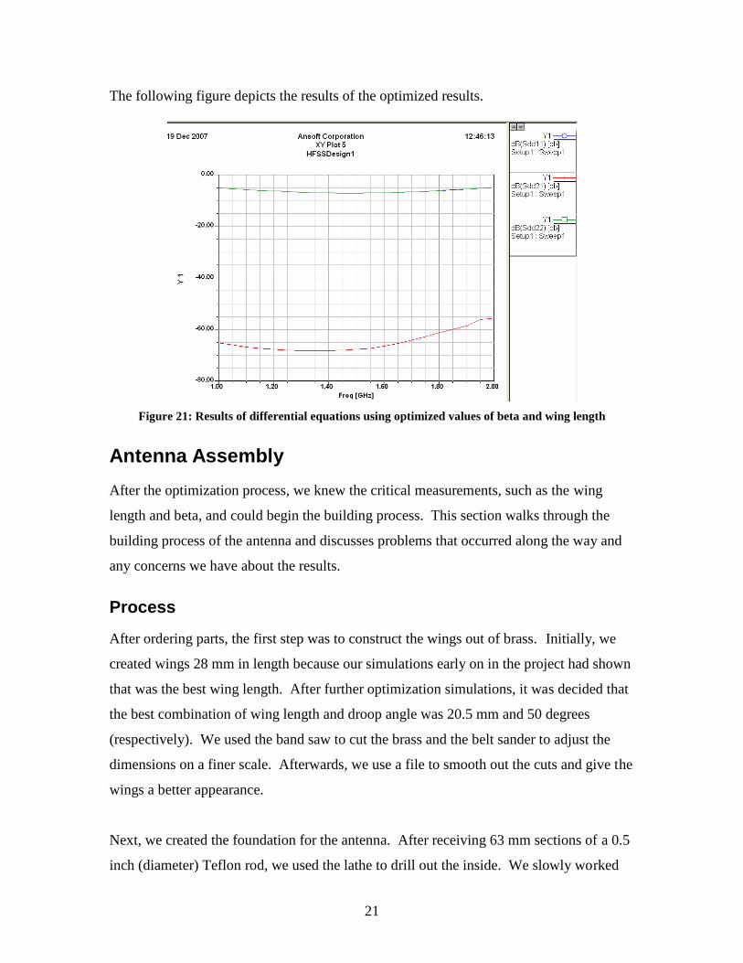
The following figure depicts the results of the optimized results.
Figure 21: Results of differential equations using optimized values of beta and wing length
Antenna Assembly
After the optimization process, we knew the critical measurements, such as the wing
length and beta, and could begin the building process. This section walks through the
building process of the antenna and discusses problems that occurred along the way and
any concerns we have about the results.
Process
After ordering parts, the first step was to construct the wings out of brass. Initially, we
created wings 28 mm in length because our simulations early on in the project had shown
that was the best wing length. After further optimization simulations, it was decided that
the best combination of wing length and droop angle was 20.5 mm and 50 degrees
(respectively). We used the band saw to cut the brass and the belt sander to adjust the
dimensions on a finer scale. Afterwards, we use a file to smooth out the cuts and give the
wings a better appearance.
Next, we created the foundation for the antenna. After receiving 63 mm sections of a 0.5
inch (diameter) Teflon rod, we used the lathe to drill out the inside. We slowly worked

22
up to a diameter that could house the four coaxial cables inside the tube. Since the PCB
vias were still outside of that diameter, we expanded the circle for about 1 cm into the
end of the tube where the PCB would be in contact.
Unfortunately, the PCBs came with a solder mask on the copper portions to which we
attached the wings. Therefore, we needed to use a razor blade in order to scratch off the
solder mask. We stripped the coaxial cables and threaded them through the tube, with the
inner conductor for each of the cables going through one of the PCB vias. Then, we
soldered the inner conductor of the coaxial cables directly to the PCB. Next, we soldered
the wings to the PCB and glued the PCB to the Teflon tube.
Problems
There existed a great difficulty in creating wings that matched the exact dimensions that
we needed. The difficulty lied in matching said dimensions to within mere millimeters.
Shortening the wings turned out to be very time consuming. However, the problem with
shortening the wings we had was that it made any inequality in the lengths of the sides of
the wings much more pronounced.
Testing
Process
In order to test the antennas, we must consider the turnstile antenna as two separate
dipole antennas that share a common balun. We must test both of these individual dipole
antennas in order to determine the return loss. We then must test the two dipole antennas
at the same time, in order to measure the interference (crosstalk) between the two
antennas. Ed Oliveira provided us with MATLAB m-files that performed calibrated tests
using the network analyzer.
S11/22 Calibration Tests
When we were measuring the individual dipoles, we connected two 50 ohm terminations
to the two ports of the dipole that was not being measured. Next, we connected the
network analyzer to port S of the 180 degree hybrid and two short standard terminations

23
to ports 1 and 2, as necessitated by the m-file. The m-file then used the network analyzer
to perform a frequency sweep from 1 to 2 GHz (as determined by the user inputs). After
the sweep, we connected the two 50 ohm standard terminations to ports 1 and 2 of the
180 degree hybrid. After the network analyzer ran another sweep, we connected the two
ports of the hybrid to the dipole antenna. After the third and final sweep was run, the m-
file produced a graph of the S11 (or S22) return loss and impedance data (both real and
complex).
S21 Calibration Tests
When we needed to measure the crosstalk, we connected both network analyzer ports to
port S of two different 180 degree hybrids. We then connected both of the port 1’s and
2’s to each other using two SMA to SMA coaxial connections. After the m-file ran a
sweep of the data, we connected one dipole to ports 1 and 2 of one of the hybrids and the
other dipole to ports 1 and 2 of the other hybrid. The m-file ran one more sweep,
producing a graph of the S21 return loss and impedance data.
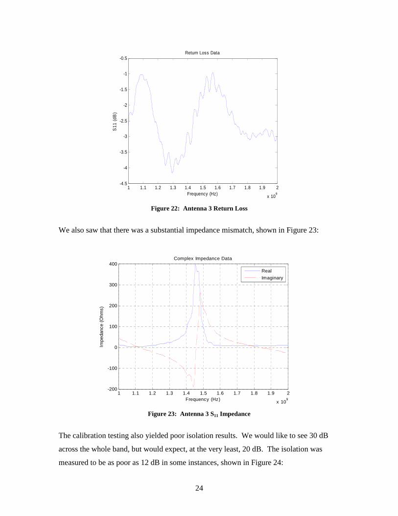
Results
The testing of this antenna yielded poor results. Ideally, we would have a frequency
range in which the return loss stays below 10 dB. This was certainly not the case. There
were times that the return loss did not even drop below 5 dB, as shown in Figure 22:
24
Figure 22: Antenna 3 Return Loss
We also saw that there was a substantial impedance mismatch, shown in Figure 23:
Figure 23: Antenna 3 S11 Impedance
The calibration testing also yielded poor isolation results. We would like to see 30 dB
across the whole band, but would expect, at the very least, 20 dB. The isolation was
measured to be as poor as 12 dB in some instances, shown in Figure 24:
1 1.1 1.2 1.3 1.4 1.5 1.6 1.7 1.8 1.9 2
x 109
-4.5
-4
-3.5
-3
-2.5
-2
-1.5
-1
-0.5Return Loss Data
Frequency (Hz)
S11
(dB
)
1 1.1 1.2 1.3 1.4 1.5 1.6 1.7 1.8 1.9 2
x 109
-200
-100
0
100
200
300
400Complex Impedance Data
Frequency (Hz)
Impe
danc
e (O
hms)
Real
Imaginary

25
Figure 24: Antenna 3 Isolation The next step was to determine whether or not the ground plane was at fault for the poor
performance of the antennas. Therefore, we ran the calibration tests without the ground
plane. Figure 25 shows the return loss of antenna 3 without a ground plane:
Figure 25: Antenna 3 Return Loss without Ground plane
Figure 26 shows the isolation of antenna 3 without a ground plane:
1 1.1 1.2 1.3 1.4 1.5 1.6 1.7 1.8 1.9 2
x 109
-26
-24
-22
-20
-18
-16
-14
-12
-10
-8Return Loss Data
Frequency (Hz)
S21
(dB
)
1 1.1 1.2 1.3 1.4 1.5 1.6 1.7 1.8 1.9 2
x 109
-16
-14
-12
-10
-8
-6
-4
-2Return Loss Data
Frequency (Hz)
S11
(dB
)

26
Figure 26: Antenna 3 Isolation without Ground plane
While taking the ground plane appeared to have helped the return loss slightly, it seems
to have hurt the isolation slightly. Nevertheless, we would expect better results. The
ground plane does not seem to be an issue. We then proceeded to tape the hybrids to the
ground plane in order to determine if having the hybrids close to each other were causing
any problems. Antenna 3’s return loss is shown in Figure 27:
Figure 27: Antenna 3 Return Loss with Hybrids taped to Ground plane
1 1.1 1.2 1.3 1.4 1.5 1.6 1.7 1.8 1.9 2
x 109
-16
-14
-12
-10
-8
-6
-4Return Loss Data
Frequency (Hz)
S21
(dB
)
1 1.1 1.2 1.3 1.4 1.5 1.6 1.7 1.8 1.9 2
x 109
-10
-9
-8
-7
-6
-5
-4
-3
-2
-1
0Return Loss Data
Frequency (Hz)
S11
(dB
)

27
This did not seem to help the return loss. The overall performance of this antenna design
was poor, and nothing that we attempted to do seemed to improve this performance. All
of the results from the calibration testing are shown in Appendix C: Testing Results of
the First Design.
First Design Conclusions The most disconcerting characteristic about the poor performance of the antennas is the
fact that the results differed so greatly from the Ansoft simulation results. This could
have been caused by one a few different variations from the simulated design. For
instance, the simulated design contained an electrically conductive sheet that connected
the center conductors of the coaxial cables to the wings.
When we built the antennas we used liquid rosin flux and solder. There existed a great
difficulty in soldering the wings to the PCB. At first, the copper wings would not form a
strong enough bond, causing antenna instability. The continual soldering eventually lead
to a couple of the copper traces on the PCB separating from the PCB, leaving only the via
to which the wing could be soldered. We overcame the antenna instability issues by
using a larger amount of liquid rosin flux before we soldered, which increased the
strength of the connected that was capable of being formed by the solder. The fact that
we had the copper pads in the corners of the PCB might have impaired the ease of
creating a good solder connection. We originally designed the PCB in such way because
we wanted to minimize crosstalk.
The center conductor of the coaxial cables did not lay completely flat on the PCB. Our
Ansoft model had center conductors that were terminated at the top of the PCB. Since
ours had a finite thickness on the PCB’s copper pad, the wings could not stay perfectly
flat, which in turn led to another notable problem. The wings were hard to solder at the
correct droop angle. Our simulations had shown that the droop angle affects the return
loss, resonance, and isolation.

28
Another solution to the stability problem involved using epoxy to help solidify the overall
structure. The epoxy was used to help keep the wings stable as well as to form a bond
between the Teflon balun and PCB. While the epoxy performed in excellent job in
increasing the antenna’s durability, it was not included Ansoft simulations. For this
reason, we cannot overlook the fact that it may very well have had a certain degree of
influence on the results. However, we could not have realistically created an antenna
using our design without the epoxy.
When we built the antennas, we stripped back the outer shielding of the coaxial cables
about 1 cm, and taped the outer conductors together, creating a ground between all of the
coaxial cable grounds. In our Ansoft model, we did not have an outer shielding for the
coaxial cables. Instead, we had a 2 mm gap between the conductors. This could have
been one of the factors that caused the experimental results to differ from the simulation
results.
The most distinctive negative trait of our antennas can easily be seen after a quick visual
test: the wings lack symmetry. When creating designs that need to be accurate to within
one or two millimeters, a small difference in one or more wings becomes a noticeable
problem. The size of the wings affected the droop angle we used in fabrication. We
could not let the wing tabs sit flat on the PCB since some of the wings would have made
contact at the corners. Such an electrical connection would have severely damaged the
antenna’s ability to operate to any degree of success.
The antenna wings may have contained flaws for a couple of different reasons. First, the
antenna wings were created by inexperienced machine operators. We were not extremely
familiar with the use of the band saw in cutting copper, and this may have contributed in
a negative manner. While every intention was made to be accurate to within a
millimeter, the difficulty may have been too great for inexperienced operators on older
equipment. It might have been better to use the shears in order to cut the wings. We had
originally avoided using the shears because we wanted to avoid any bending of the

29
copper, especially given the thickness of the wings we were using. The copper that we
used for the wings needed to be relatively thick because the wings had to be durable.
While the four coaxial cable Dyson balun design was good idealistically, it proved to
rather difficult to fabricate accurate to the simulation. Combined with the stability
problems, it proved to be impractical. Since we did not have any antenna fabrication
experience, we were not aware of the difficulties that might have been associated with
our design.
New Antenna Design
The previous design did not meet requirements. For our new design we will continue to
use the Dyson balun but instead of coaxial cables we will use a quad line. Some
modifications will need to be made to accommodate this change. The following section
describes the modified parts and design for the new antenna.
Parts
Printed Circuit Board Design
Since we were merely modifying a design that had already been built, the main priority
was to redesign everything that needed changing, which was primarily the PCB. We
needed to perform a small amount of microstrip transmission line analysis in order to
determine the proper dimensions for the PCB.
From the charts on p. 66 of Ludwig/Bretchko, we estimate the w/h (width to height) ratio
for a 50 ohm microstrip transmission line on FR-4 to be approximately 1.8 to 2. We can
assume that the w/h ratio is between one and two. For w/h ≤ 2, the following equation
gives the exact value of w/h:
2
82 −
=A
A
e
e
h
w (3)
The quantity A is a constant defined by the following equation:

30
+
+−++⋅⋅=
rr
rr
O
OZA
εεεε
ηπ 11.0
23.01
1
2
12 (4)
Zo is defined as the characteristic impedance of the transmission line. We want the
characteristic impedance to be 50 ohms. FR-4 has a relative dielectric constant that
ranges from 4.2 to 4.6. For this reason, we used the middle value in the range, 4.4. ηo is
defined as the impedance of space in a vacuum, which is given by the following equation:
7.376/1085418.8
/10412
7
≈⋅
⋅== −
−
mF
mH
o
oo
πεµη (5)
If we substitute the appropriate values into equation 4 we arrive at the following value for
A:
531.14.4
11.023.0
14.4
14.4
2
14.4
7.376
502 =
++−++⋅
ΩΩ⋅= πA (6)
We can then substitute the value we found for A into equation 3:
91.12
8531.12
531.1
=−
= ⋅e
e
h
w (7)
Before we use this ratio, we need to verify that a microstrip transmission line with a
width to height ratio of 1.91 will have a characteristic impedance of 50 ohms. First, we
need to find the effective dielectric constant. Since our width is greater than the height,
we need to use the formula for wide transmission lines:
3.3)91.1
1121(
2
14.4
2
14.4)121(
2
1
2
1 2/12/1 =⋅+−++=+−++= −−
w
hrreff
εεε (8)
Using this value, we can now find the characteristic impedance:

31
))444.1ln(3
2393.1( +++
=
h
w
h
wZ
eff
OO
ε
η (9)
If we insert the appropriate values:
Ω=+++
Ω= 46.50))444.191.1ln(
3
291.1393.1(3.3
7.376OZ
(10)
This value differs from the expected value due to rounding error. Since we are using a
PCB with a height of 62 mils, we can calculate the width of the microstrip line to be
118.42 mils, or 3.0 millimeters.
Next, we need to determine the appropriate length for the 4 traces. We need to calculate
the length of the wave propagating down the microstrip line at the center frequency of the
frequency range:
mms
sm
f
c
eff
95.1263.3103.1
/29979245819
=⋅
==−ε
λ (11)
Since we want the length of the traces to be a quarter of the wavelength, we can
determine that the length of our microstrip lines should be 31.7 mm.
Balun
The new design contains a four microstrip transmission balun. Each transmission line
contains two copper microstrips with Rogers duroid in the middle. Each transmission
line measures 50 mils in thickness, and is has one microstrip line face soldered to a
rectangular copper center conductor containing a 1.2 mm by 1.2 mm cross section. The
dimensions of the balun are given in Figure 28:

32
Figure 28: Cross Sectional Balun Dimensions The height of the balun was designed to be 1.77 inches.
Antenna Fabrication The most laborious part of the building the newly designed antennas was creating the
Teflon block. We had to start with Teflon cylinder that measured 4 inches in diameter
and 4 inches high. We then used the lathe to square off both sides. Next we used the
Bridgeport machine in order to mill down the cylinder into a block that measured 2.75
inches by 2.75 inches and 1.77 inches tall, shown in Figure 29:
Figure 29: Teflon Block

33
Next, we used calipers to create tick marks on the Teflon block for the angles. Using the
Bridgeport, we were able to create each of the four angled faces. Since the Bridgeport
could keep the Teflon pyramid square, we used it to drill the hole through the center of
the Teflon block. Using an end mill attachment to the Bridgeport machine, we created
two troughs in line with the center hole of the pyramid, in order to allow for the solder
needed for connecting the balun to the PCB and the four coaxial cable connectors to the
PCB. This led to the creating of the pyramid shown in Figure 30:
Figure 30: Completed Teflon Pyramid The next step in the manufacturing process was creating the balun. We needed to cut out
a center conductor out of a piece of stock copper using the Bridgeport machine. Next, we
needed to use the shears to cut the four microstip transmission lines out of the larger
board. For the antenna with the center conductor measuring 1.2 mm by 1.2 mm, we were
able to use a jig created by Patrick Morrison of the ECE shop in order to solder the four
transmission lines to the center conductor. The jig is shown in Figure 31:
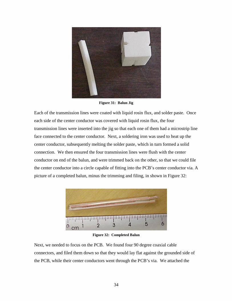
34
Figure 31: Balun Jig Each of the transmission lines were coated with liquid rosin flux, and solder paste. Once
each side of the center conductor was covered with liquid rosin flux, the four
transmission lines were inserted into the jig so that each one of them had a microstrip line
face connected to the center conductor. Next, a soldering iron was used to heat up the
center conductor, subsequently melting the solder paste, which in turn formed a solid
connection. We then ensured the four transmission lines were flush with the center
conductor on end of the balun, and were trimmed back on the other, so that we could file
the center conductor into a circle capable of fitting into the PCB’s center conductor via. A
picture of a completed balun, minus the trimming and filing, in shown in Figure 32:
Figure 32: Completed Balun Next, we needed to focus on the PCB. We found four 90 degree coaxial cable
connectors, and filed them down so that they would lay flat against the grounded side of
the PCB, while their center conductors went through the PCB’s via. We attached the

35
cables to the connectors, soldered the connectors to the PCB, and then soldered the balun
to the PCB.
We determined, after our experience with our first design, that the best way to create the
wings would be to use the shears. Since the wings were going to lie flat on a Teflon
pyramid, we did not need to focus on creating extremely durable wings, consequently
allowing us to create the wings thinner. This was very important, since thinner brass is
easier to shear accurately. Once the wings were created, we put the Teflon pyramid on
top of the PCB, with balun going through the pyramid’s central hole. After soldering the
wings to the balun, we proceeded with the calibration testing.
Testing Results The initial calibration testing results did not produce positive results. The return loss was
lower than an acceptable level, as shown in Figure 33:
Figure 33: 1.2mm Center Conductor Antenna 1 S11
The isolation was measured to be unsatisfactory:
1 1.1 1.2 1.3 1.4 1.5 1.6 1.7 1.8 1.9 2
x 109
-12
-11
-10
-9
-8
-7
-6
-5
-4
-3
-2Return Loss Data
Frequency (Hz)
S11
(dB
)
36
Figure 34: 1.2mm Center Conductor Antenna 1 S11 Impedance
In order to trouble shoot the problem, we took removed the wings and Teflon pyramid,
and retested the isolation, ascertaining the results shown in Figure 35:
Figure 35: Antenna 1 S21 Measured without Teflon or Wings
Since this seemed to improve the performance of the antenna, we put the Teflon pyramid
on top of the PCB again and retested the antenna’s isolation in order to determine
1 1.1 1.2 1.3 1.4 1.5 1.6 1.7 1.8 1.9 2
x 109
-200
-100
0
100
200
300
400Complex Impedance Data
Frequency (Hz)
Impe
danc
e (O
hms)
Real
Imaginary
1 1.1 1.2 1.3 1.4 1.5 1.6 1.7 1.8 1.9 2
x 109
-38
-36
-34
-32
-30
-28
-26
-24
-22
-20
-18Return Loss Data
Frequency (Hz)
S21
(dB
)

37
whether or not the wings were the root cause of the poor performance. The result is
shown in Figure 36:
Figure 36: Antenna 1 S21 Measured with Teflon, without Wings
It appeared the Teflon pyramid seemed to be causing the poor performance of the
antenna. In order to side step this issue, we decided (per the instruction of Professor
Makarov) to increase the balun size and redesign the PCB accordingly.
We redesigned the balun so that the center conductor’s cross section measured 2 mm by 2
mm, as shown in Figure 37:
1 1.1 1.2 1.3 1.4 1.5 1.6 1.7 1.8 1.9 2
x 109
-32
-30
-28
-26
-24
-22
-20
-18
-16
-14
-12Return Loss Data
Frequency (Hz)
S21
(dB
)

38
Figure 37: 2 mm Antenna Balun Cross Section
Calibration testing produced the following return loss for S11:
Figure 38: 2 mm Antenna S11
Calibration testing produced the following return loss for S22:
1 1.1 1.2 1.3 1.4 1.5 1.6 1.7 1.8 1.9 2
x 109
-9
-8
-7
-6
-5
-4
-3
-2Return Loss Data
Frequency (Hz)
S11
(dB
)
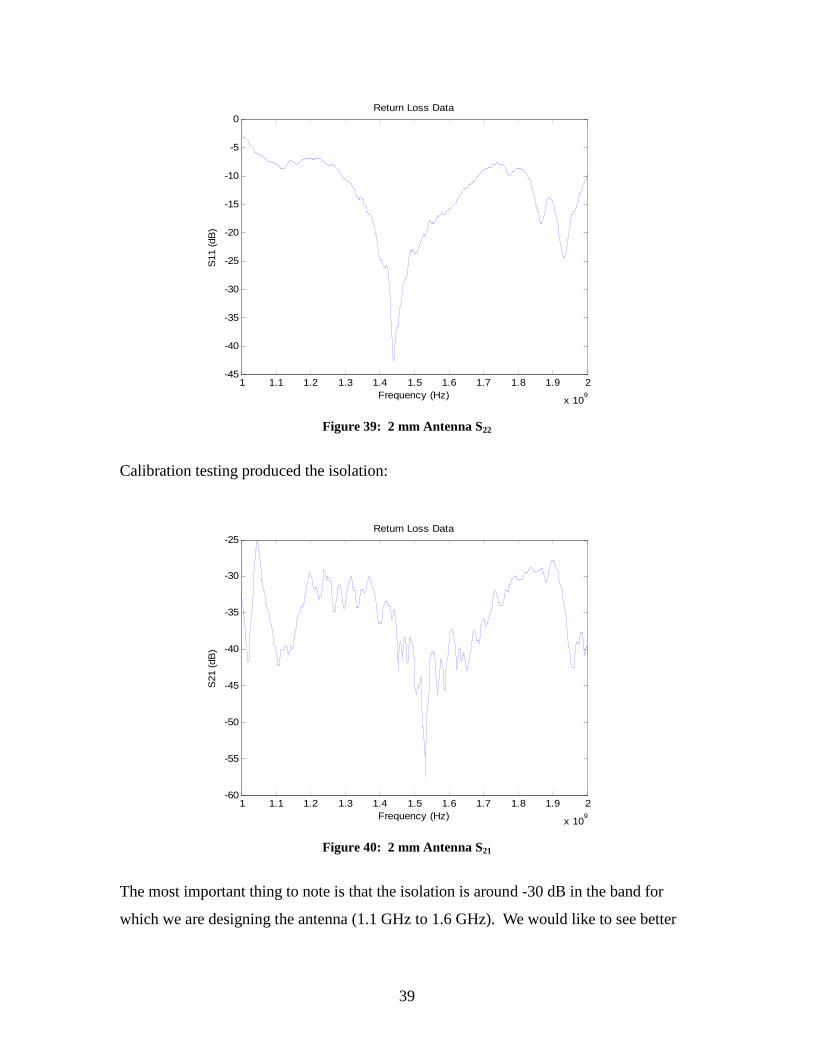
39
Figure 39: 2 mm Antenna S22
Calibration testing produced the isolation:
Figure 40: 2 mm Antenna S21
The most important thing to note is that the isolation is around -30 dB in the band for
which we are designing the antenna (1.1 GHz to 1.6 GHz). We would like to see better
1 1.1 1.2 1.3 1.4 1.5 1.6 1.7 1.8 1.9 2
x 109
-45
-40
-35
-30
-25
-20
-15
-10
-5
0Return Loss Data
Frequency (Hz)
S11
(dB
)
1 1.1 1.2 1.3 1.4 1.5 1.6 1.7 1.8 1.9 2
x 109
-60
-55
-50
-45
-40
-35
-30
-25Return Loss Data
Frequency (Hz)
S21
(dB
)
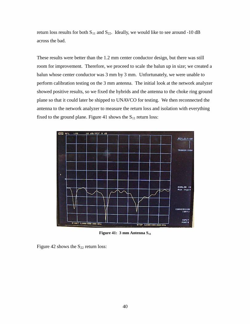
40
return loss results for both S11 and S22. Ideally, we would like to see around -10 dB
across the bad.
These results were better than the 1.2 mm center conductor design, but there was still
room for improvement. Therefore, we proceed to scale the balun up in size; we created a
balun whose center conductor was 3 mm by 3 mm. Unfortunately, we were unable to
perform calibration testing on the 3 mm antenna. The initial look at the network analyzer
showed positive results, so we fixed the hybrids and the antenna to the choke ring ground
plane so that it could later be shipped to UNAVCO for testing. We then reconnected the
antenna to the network analyzer to measure the return loss and isolation with everything
fixed to the ground plane. Figure 41 shows the S11 return loss:
Figure 41: 3 mm Antenna S11
Figure 42 shows the S22 return loss:

41
Figure 42: 3 mm Antenna S22
Figure 43 shows the isolation:
Figure 43: 3 mm Antenna S21
Next, we connected both of the 180° hybrids to a 90° in order to produce RHCP. We then
drove the 90° hybrid with port 1 of the network analyzer and took a picture of the results:
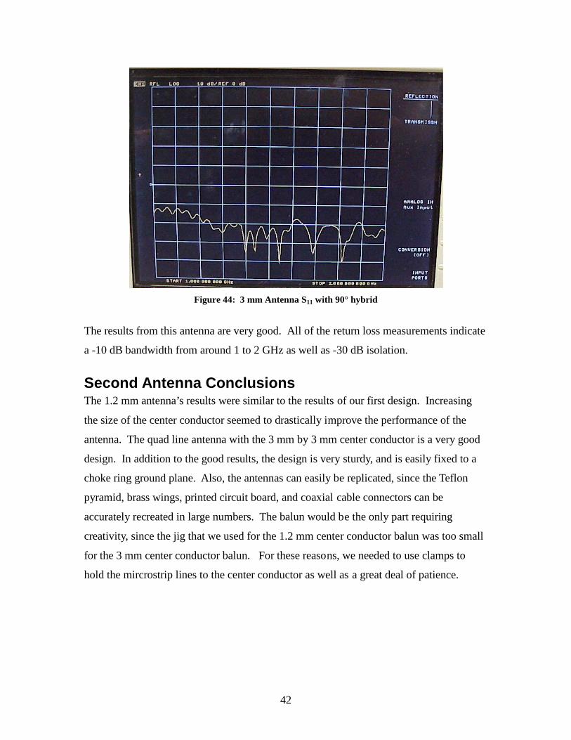
42
Figure 44: 3 mm Antenna S11 with 90° hybrid
The results from this antenna are very good. All of the return loss measurements indicate
a -10 dB bandwidth from around 1 to 2 GHz as well as -30 dB isolation.
Second Antenna Conclusions The 1.2 mm antenna’s results were similar to the results of our first design. Increasing
the size of the center conductor seemed to drastically improve the performance of the
antenna. The quad line antenna with the 3 mm by 3 mm center conductor is a very good
design. In addition to the good results, the design is very sturdy, and is easily fixed to a
choke ring ground plane. Also, the antennas can easily be replicated, since the Teflon
pyramid, brass wings, printed circuit board, and coaxial cable connectors can be
accurately recreated in large numbers. The balun would be the only part requiring
creativity, since the jig that we used for the 1.2 mm center conductor balun was too small
for the 3 mm center conductor balun. For these reasons, we needed to use clamps to
hold the mircrostrip lines to the center conductor as well as a great deal of patience.

43
The follwing figures depict the final antenna attached to the ground plane:
Figure 45: Final Design Top View
Figure 46: Final Design Bottom View

44
Figure 47: Final Design Side View

45
Appendix A: Design Parameters
Figure 48: Design parameters for first design
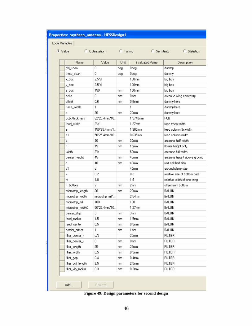
46
Figure 49: Design parameters for second design

47
Appendix B: MATLAB Code
All MATLAB calibration testing code was provided by Eduardo Oliveira.
S11 Calibration
%S11 calibration
%fun with freq resp emo
%Ed Oliveira
%Oct 15 2007
% based on MVL code
% fixed transmission line impedance rotation
%clear
%startf=0.550e9;
startf=1e9;
%stopf=0.7e9;
stopf=2e9;
fstep=.4e6;
%fstep=5e4;
startf=input( 'Input start frequency in Hz:' )
stopf=input( '\nInput stop frequency in Hz:' )
%freqs =
linspace(freq_resp_lib.start,freq_resp_lib.stop,num el(freq_resp_lib.fre
q_data));
freqs= (startf:fstep:stopf);
fprintf( '\nConnect GPIB cable between computer and network analyzer' )
input( ' and press return\n' )
fprintf( 'Connect the short standard to the end of the input cable' )
input( ' and press return\n' )
freq_resp_lib = get_freq_resp(startf, stopf, fste p, 'S11' );
freq_resp_lib.freq_data = conj(freq_resp_lib.freq_d ata);
s11short=freq_resp_lib.freq_data;

48
fprintf( 'Connect the 50 ohm standard to the end of the inpu t cable' )
input( ' and press return\n' )
freq_resp_lib = get_freq_resp(startf, stopf, fste p, 'S11' );
freq_resp_lib.freq_data = conj(freq_resp_lib.freq_d ata);
s11matched=freq_resp_lib.freq_data;
fprintf( 'Connect the antenna to the end of the input cable' )
input( ' and press return\n' )
freq_resp_lib = get_freq_resp(startf, stopf, fste p, 'S11' );
freq_resp_lib.freq_data = conj(freq_resp_lib.freq_d ata);
s11rot=freq_resp_lib.freq_data;
freq_resp_lib.freq_data=(s11rot-s11matched)./(s11ma tched-s11short);
Zt = 50*(freq_resp_lib.freq_data + 1)./(1- freq_r esp_lib.freq_data);
figure(1);
plot(freqs,20*log10(abs(freq_resp_lib.freq_data))), title ( 'Return Loss
Data' ), xlabel ( 'Frequency (Hz)' ), ylabel( 'S11 (dB)' );
figure(2)
plot(freqs,real(Zt)), title ( 'Complex Impedance Data' ), xlabel
( 'Frequency (Hz)' ), ylabel ( 'Impedance (Ohms)' );
hold on; grid on;
plot(freqs,imag(Zt), 'r--' );
legend ( 'Real' , 'Imaginary' );
hold off
%figure(2)
%plot(freqs,(real(freq_resp_lib.freq_data)));
%subplot(3,1,3);
%figure(3)
%plot(freqs,(imag(freq_resp_lib.freq_data)));
%line(freqs,unwrap(angle(freq_resp_lib.freq_data))) ;
% figure(2);
% subplot(3,1,1);
% plot(freqs,abs(Impedance));
% subplot(3,1,2);
% plot(freqs,real(Impedance));
% subplot(3,1,3);

49
% plot(freqs,imag(Impedance));
S21 Calibration
%S11 calibration
%fun with freq resp emo
%Ed Oliveira
%Oct 15 2007
% based on MVL code
% fixed transmission line impedance rotation
clear;
%startf=0.550e9;
startf=1e9;
%stopf=0.7e9;
stopf=2e9;
fstep=.4e6;
%fstep=5e4;
%freqs =
linspace(freq_resp_lib.start,freq_resp_lib.stop,num el(freq_resp_lib.fre
q_data));
freqs= (startf:fstep:stopf);
fprintf( 'Connect GPIB cable between computer and network an alyzer' )
input( ' and press return\n' )
fprintf( 'Connect the Through standard to the end of the inp ut cable' )
input( ' and press return\n' )
freq_resp_lib = get_freq_resp(startf, stopf, fste p, 'S21' );
freq_resp_lib.freq_data = conj(freq_resp_lib.freq_d ata);
s11through=freq_resp_lib.freq_data;
% fprintf('Connect the 50 ohm standard to the end o f the input cable')
% input(' and press return\n')
% freq_resp_lib = get_freq_resp(startf, stopf, fs tep, 'S11');
% freq_resp_lib.freq_data = conj(freq_resp_lib.freq _data);
% s11matched=freq_resp_lib.freq_data;

50
fprintf( 'Connect the antenna to the end of the input cable' )
input( ' and press return\n' )
freq_resp_lib = get_freq_resp(startf, stopf, fste p, 'S21' );
freq_resp_lib.freq_data = conj(freq_resp_lib.freq_d ata);
s11rot=freq_resp_lib.freq_data;
freq_resp_lib.freq_data=(s11rot)./(s11through);
Zt = 50*(freq_resp_lib.freq_data + 1)./(1- freq_r esp_lib.freq_data);
figure(1);
plot(freqs,20*log10(abs(freq_resp_lib.freq_data))), title ( 'Return Loss
Data' ), xlabel ( 'Frequency (Hz)' ), ylabel( 'S21 (dB)' );
figure(2)
plot(freqs,real(Zt)), title ( 'Complex Impedance Data' ), xlabel
( 'Frequency (Hz)' ), ylabel ( 'Impedance (Ohms)' );
hold on; grid on;
plot(freqs,imag(Zt), 'r--' );
legend ( 'Real' , 'Imaginary' );
hold off
%figure(2)
%plot(freqs,(real(freq_resp_lib.freq_data)));
%subplot(3,1,3);
%figure(3)
%plot(freqs,(imag(freq_resp_lib.freq_data)));
%line(freqs,unwrap(angle(freq_resp_lib.freq_data))) ;
% figure(2);
% subplot(3,1,1);
% plot(freqs,abs(Impedance));
% subplot(3,1,2);
% plot(freqs,real(Impedance));
% subplot(3,1,3);
% plot(freqs,imag(Impedance));
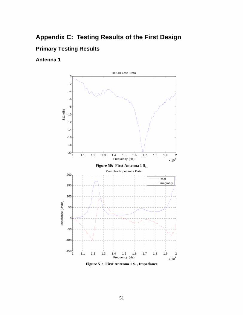
51
Appendix C: Testing Results of the First Design
Primary Testing Results
Antenna 1
Figure 50: First Antenna 1 S11
Figure 51: First Antenna 1 S11 Impedance
1 1.1 1.2 1.3 1.4 1.5 1.6 1.7 1.8 1.9 2
x 109
-20
-18
-16
-14
-12
-10
-8
-6
-4
-2
0Return Loss Data
Frequency (Hz)
S11
(dB
)
1 1.1 1.2 1.3 1.4 1.5 1.6 1.7 1.8 1.9 2
x 109
-150
-100
-50
0
50
100
150
200Complex Impedance Data
Frequency (Hz)
Impe
danc
e (O
hms)
Real
Imaginary

52
Figure 52: Second Antenna 1 S11
Figure 53: Second Antenna 1 S11 Impedance
1 1.1 1.2 1.3 1.4 1.5 1.6 1.7 1.8 1.9 2
x 109
-25
-20
-15
-10
-5
0Return Loss Data
Frequency (Hz)
S11
(dB
)
1 1.1 1.2 1.3 1.4 1.5 1.6 1.7 1.8 1.9 2
x 109
-100
-50
0
50
100
150
200
250Complex Impedance Data
Frequency (Hz)
Impe
danc
e (O
hms)
Real
Imaginary
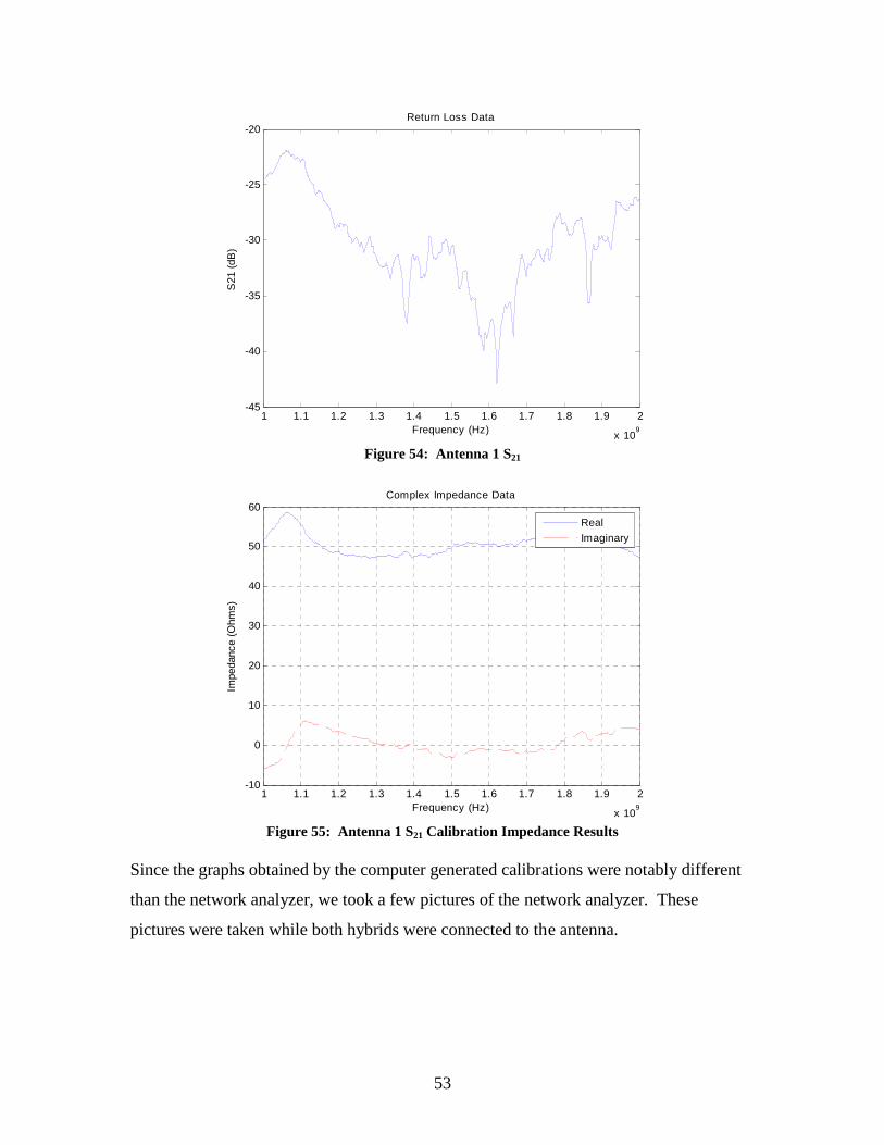
53
Figure 54: Antenna 1 S21
Figure 55: Antenna 1 S21 Calibration Impedance Results
Since the graphs obtained by the computer generated calibrations were notably different
than the network analyzer, we took a few pictures of the network analyzer. These
pictures were taken while both hybrids were connected to the antenna.
1 1.1 1.2 1.3 1.4 1.5 1.6 1.7 1.8 1.9 2
x 109
-45
-40
-35
-30
-25
-20Return Loss Data
Frequency (Hz)
S21
(dB
)
1 1.1 1.2 1.3 1.4 1.5 1.6 1.7 1.8 1.9 2
x 109
-10
0
10
20
30
40
50
60Complex Impedance Data
Frequency (Hz)
Impe
danc
e (O
hms)
Real
Imaginary
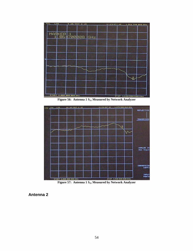
54
Figure 56: Antenna 1 S11 Measured by Network Analyzer
Figure 57: Antenna 1 S21 Measured by Network Analyzer
Antenna 2

55
Figure 58: Antenna 2 S11
Figure 59: Antenna 2 S11 Impedance
1 1.1 1.2 1.3 1.4 1.5 1.6 1.7 1.8 1.9 2
x 109
-4.5
-4
-3.5
-3
-2.5
-2
-1.5
-1
-0.5Return Loss Data
Frequency (Hz)
S11
(dB
)
1 1.1 1.2 1.3 1.4 1.5 1.6 1.7 1.8 1.9 2
x 109
-200
-100
0
100
200
300
400Complex Impedance Data
Frequency (Hz)
Impe
danc
e (O
hms)
Real
Imaginary

56
Figure 60: Antenna 2 S21
Figure 61: Antenna 2 S21 Impedance
1 1.1 1.2 1.3 1.4 1.5 1.6 1.7 1.8 1.9 2
x 109
-50
-45
-40
-35
-30
-25
-20
-15Return Loss Data
Frequency (Hz)
S21
(dB
)
1 1.1 1.2 1.3 1.4 1.5 1.6 1.7 1.8 1.9 2
x 109
-20
-10
0
10
20
30
40
50
60
70Complex Impedance Data
Frequency (Hz)
Impe
danc
e (O
hms)
Real
Imaginary

57
Figure 62: Antenna S21 Measured by Network Analyzer
Antenna 3
Figure 63: Antenna 3 S11
1 1.1 1.2 1.3 1.4 1.5 1.6 1.7 1.8 1.9 2
x 109
-18
-16
-14
-12
-10
-8
-6
-4
-2
0Return Loss Data
Frequency (Hz)
S11
(dB
)

58
Figure 64: Antenna 3 S11 Impedance
Figure 65: Antenna 3 S21
1 1.1 1.2 1.3 1.4 1.5 1.6 1.7 1.8 1.9 2
x 109
-100
-50
0
50
100
150
200Complex Impedance Data
Frequency (Hz)
Impe
danc
e (O
hms)
Real
Imaginary
1 1.1 1.2 1.3 1.4 1.5 1.6 1.7 1.8 1.9 2
x 109
-26
-24
-22
-20
-18
-16
-14
-12
-10
-8Return Loss Data
Frequency (Hz)
S21
(dB
)
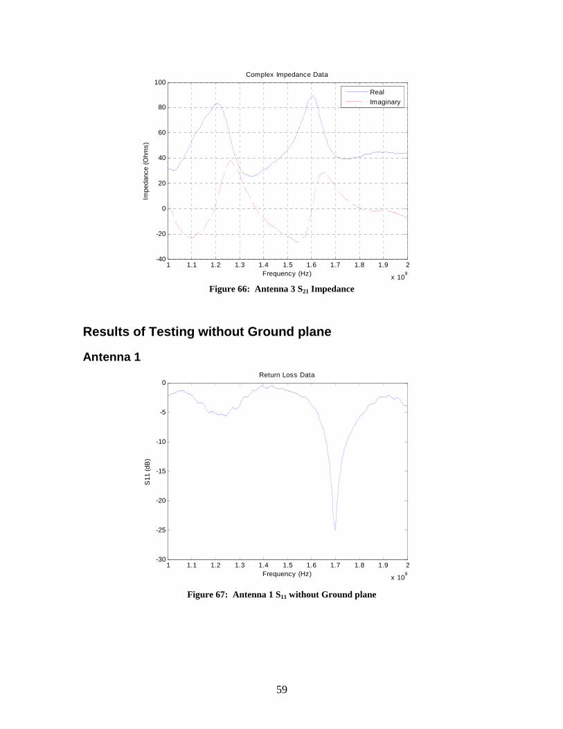
59
Figure 66: Antenna 3 S21 Impedance
Results of Testing without Ground plane
Antenna 1
Figure 67: Antenna 1 S11 without Ground plane
1 1.1 1.2 1.3 1.4 1.5 1.6 1.7 1.8 1.9 2
x 109
-40
-20
0
20
40
60
80
100Complex Impedance Data
Frequency (Hz)
Impe
danc
e (O
hms)
Real
Imaginary
1 1.1 1.2 1.3 1.4 1.5 1.6 1.7 1.8 1.9 2
x 109
-30
-25
-20
-15
-10
-5
0Return Loss Data
Frequency (Hz)
S11
(dB
)

60
Figure 68: Antenna 1 S11 Impedance without Ground plane
Figure 69: Antenna 1 S22 without Ground plane
1 1.1 1.2 1.3 1.4 1.5 1.6 1.7 1.8 1.9 2
x 109
-100
-50
0
50
100
150
200
250Complex Impedance Data
Frequency (Hz)
Impe
danc
e (O
hms)
Real
Imaginary
1 1.1 1.2 1.3 1.4 1.5 1.6 1.7 1.8 1.9 2
x 109
-30
-25
-20
-15
-10
-5
0Return Loss Data
Frequency (Hz)
S11
(dB
)

61
Figure 70: Antenna 1 S22 Impedance without Ground plane
Figure 71: Antenna 1 S21 without Ground plane
1 1.1 1.2 1.3 1.4 1.5 1.6 1.7 1.8 1.9 2
x 109
-100
-50
0
50
100
150
200Complex Impedance Data
Frequency (Hz)
Impe
danc
e (O
hms)
Real
Imaginary
1 1.1 1.2 1.3 1.4 1.5 1.6 1.7 1.8 1.9 2
x 109
-24
-22
-20
-18
-16
-14
-12
-10
-8
-6
-4Return Loss Data
Frequency (Hz)
S21
(dB
)
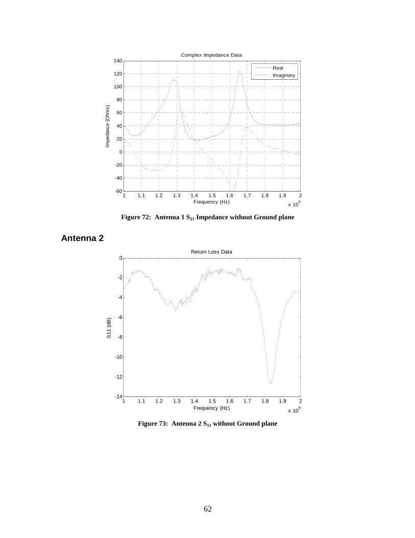
62
Figure 72: Antenna 1 S21 Impedance without Ground plane
Antenna 2
Figure 73: Antenna 2 S11 without Ground plane
1 1.1 1.2 1.3 1.4 1.5 1.6 1.7 1.8 1.9 2
x 109
-60
-40
-20
0
20
40
60
80
100
120
140Complex Impedance Data
Frequency (Hz)
Impe
danc
e (O
hms)
Real
Imaginary
1 1.1 1.2 1.3 1.4 1.5 1.6 1.7 1.8 1.9 2
x 109
-14
-12
-10
-8
-6
-4
-2
0Return Loss Data
Frequency (Hz)
S11
(dB
)
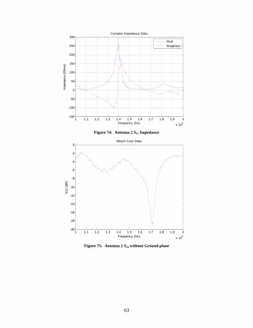
63
Figure 74: Antenna 2 S11 Impedance
Figure 75: Antenna 2 S22 without Ground plane
1 1.1 1.2 1.3 1.4 1.5 1.6 1.7 1.8 1.9 2
x 109
-150
-100
-50
0
50
100
150
200
250
300Complex Impedance Data
Frequency (Hz)
Impe
danc
e (O
hms)
Real
Imaginary
1 1.1 1.2 1.3 1.4 1.5 1.6 1.7 1.8 1.9 2
x 109
-20
-18
-16
-14
-12
-10
-8
-6
-4
-2
0Return Loss Data
Frequency (Hz)
S11
(dB
)

64
Figure 76: Antenna 2 S22 Impedance without Ground plane
Figure 77: Antenna 2 S21 without Ground plane
1 1.1 1.2 1.3 1.4 1.5 1.6 1.7 1.8 1.9 2
x 109
-100
-50
0
50
100
150
200Complex Impedance Data
Frequency (Hz)
Impe
danc
e (O
hms)
Real
Imaginary
1 1.1 1.2 1.3 1.4 1.5 1.6 1.7 1.8 1.9 2
x 109
-70
-60
-50
-40
-30
-20
-10Return Loss Data
Frequency (Hz)
S21
(dB
)
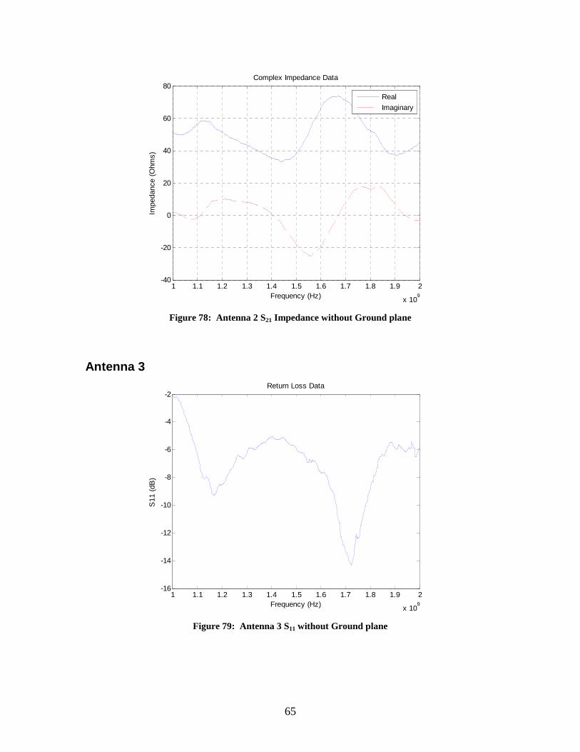
65
Figure 78: Antenna 2 S21 Impedance without Ground plane
Antenna 3
Figure 79: Antenna 3 S11 without Ground plane
1 1.1 1.2 1.3 1.4 1.5 1.6 1.7 1.8 1.9 2
x 109
-40
-20
0
20
40
60
80Complex Impedance Data
Frequency (Hz)
Impe
danc
e (O
hms)
Real
Imaginary
1 1.1 1.2 1.3 1.4 1.5 1.6 1.7 1.8 1.9 2
x 109
-16
-14
-12
-10
-8
-6
-4
-2Return Loss Data
Frequency (Hz)
S11
(dB
)
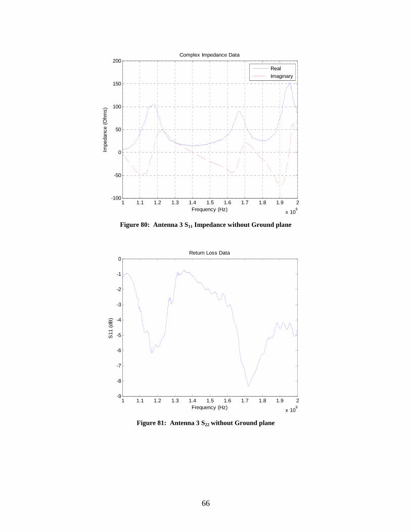
66
Figure 80: Antenna 3 S11 Impedance without Ground plane
Figure 81: Antenna 3 S22 without Ground plane
1 1.1 1.2 1.3 1.4 1.5 1.6 1.7 1.8 1.9 2
x 109
-100
-50
0
50
100
150
200Complex Impedance Data
Frequency (Hz)
Impe
danc
e (O
hms)
Real
Imaginary
1 1.1 1.2 1.3 1.4 1.5 1.6 1.7 1.8 1.9 2
x 109
-9
-8
-7
-6
-5
-4
-3
-2
-1
0Return Loss Data
Frequency (Hz)
S11
(dB
)
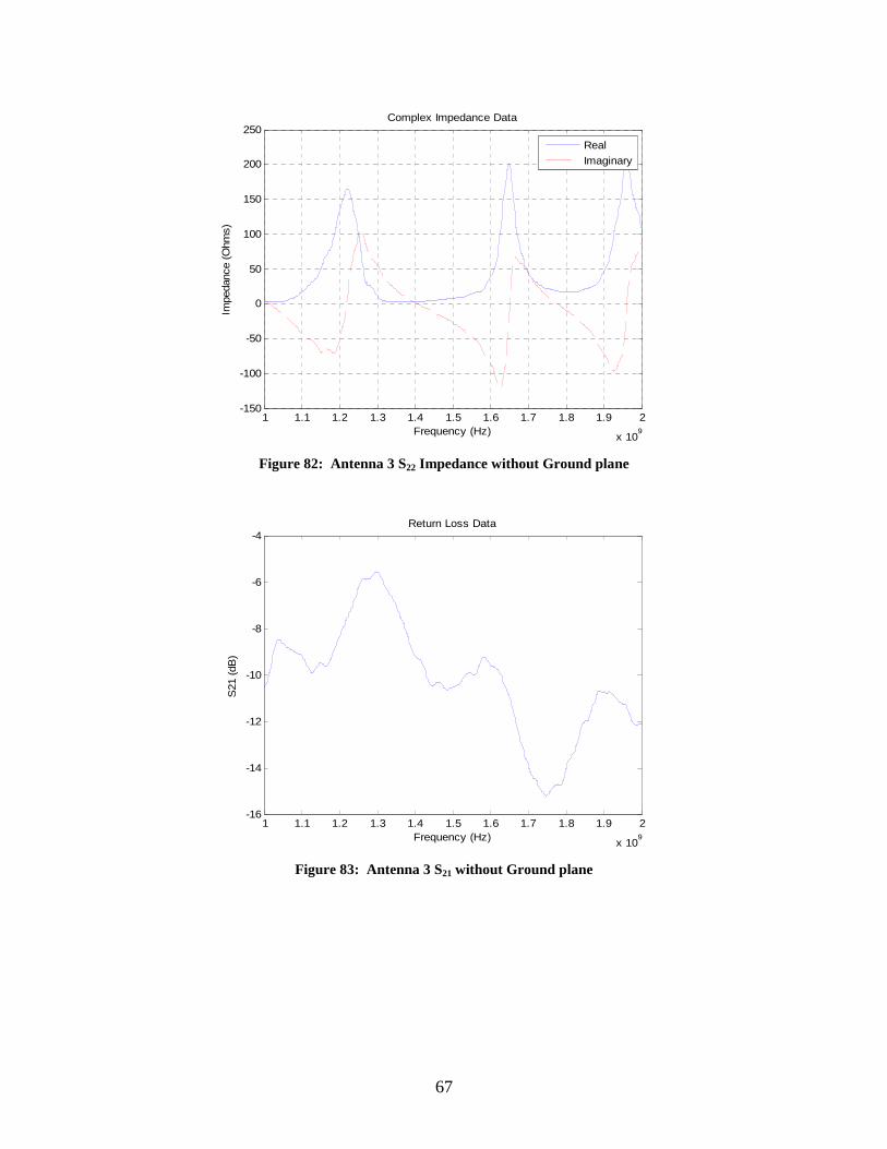
67
Figure 82: Antenna 3 S22 Impedance without Ground plane
Figure 83: Antenna 3 S21 without Ground plane
1 1.1 1.2 1.3 1.4 1.5 1.6 1.7 1.8 1.9 2
x 109
-150
-100
-50
0
50
100
150
200
250Complex Impedance Data
Frequency (Hz)
Impe
danc
e (O
hms)
Real
Imaginary
1 1.1 1.2 1.3 1.4 1.5 1.6 1.7 1.8 1.9 2
x 109
-16
-14
-12
-10
-8
-6
-4Return Loss Data
Frequency (Hz)
S21
(dB
)
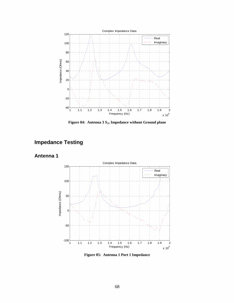
68
Figure 84: Antenna 3 S21 Impedance without Ground plane
Impedance Testing
Antenna 1
Figure 85: Antenna 1 Port 1 Impedance
1 1.1 1.2 1.3 1.4 1.5 1.6 1.7 1.8 1.9 2
x 109
-40
-20
0
20
40
60
80
100
120Complex Impedance Data
Frequency (Hz)
Impe
danc
e (O
hms)
Real
Imaginary
1 1.1 1.2 1.3 1.4 1.5 1.6 1.7 1.8 1.9 2
x 109
-100
-50
0
50
100
150Complex Impedance Data
Frequency (Hz)
Impe
danc
e (O
hms)
Real
Imaginary

69
Figure 86: Antenna 1 Port 2 Impedance
Figure 87: Antenna 1 Port 3 Impedance
1 1.1 1.2 1.3 1.4 1.5 1.6 1.7 1.8 1.9 2
x 109
-100
-50
0
50
100
150
200Complex Impedance Data
Frequency (Hz)
Impe
danc
e (O
hms)
Real
Imaginary
1 1.1 1.2 1.3 1.4 1.5 1.6 1.7 1.8 1.9 2
x 109
-100
-50
0
50
100
150
200Complex Impedance Data
Frequency (Hz)
Impe
danc
e (O
hms)
Real
Imaginary
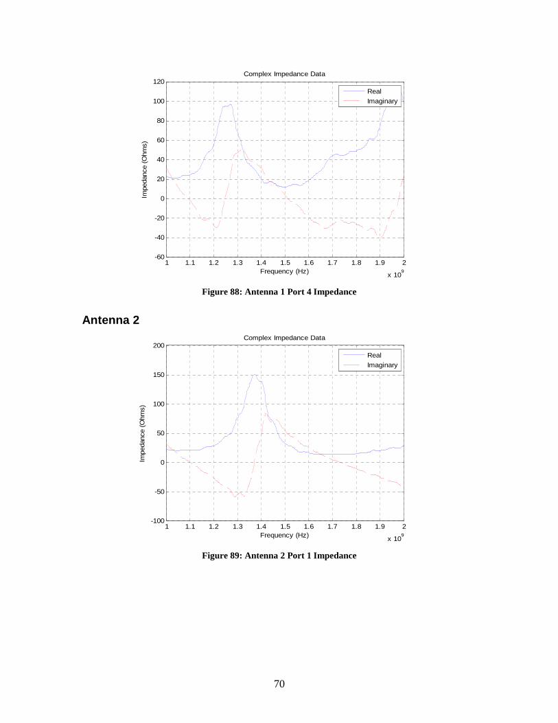
70
Figure 88: Antenna 1 Port 4 Impedance
Antenna 2
Figure 89: Antenna 2 Port 1 Impedance
1 1.1 1.2 1.3 1.4 1.5 1.6 1.7 1.8 1.9 2
x 109
-60
-40
-20
0
20
40
60
80
100
120Complex Impedance Data
Frequency (Hz)
Impe
danc
e (O
hms)
Real
Imaginary
1 1.1 1.2 1.3 1.4 1.5 1.6 1.7 1.8 1.9 2
x 109
-100
-50
0
50
100
150
200Complex Impedance Data
Frequency (Hz)
Impe
danc
e (O
hms)
Real
Imaginary

71
Figure 90: Antenna 2 Port 2 Impedance
Figure 91: Antenna 2 Port 3 Impedance
1 1.1 1.2 1.3 1.4 1.5 1.6 1.7 1.8 1.9 2
x 109
-100
-50
0
50
100
150
200Complex Impedance Data
Frequency (Hz)
Impe
danc
e (O
hms)
Real
Imaginary
1 1.1 1.2 1.3 1.4 1.5 1.6 1.7 1.8 1.9 2
x 109
-100
-50
0
50
100
150
200Complex Impedance Data
Frequency (Hz)
Impe
danc
e (O
hms)
Real
Imaginary
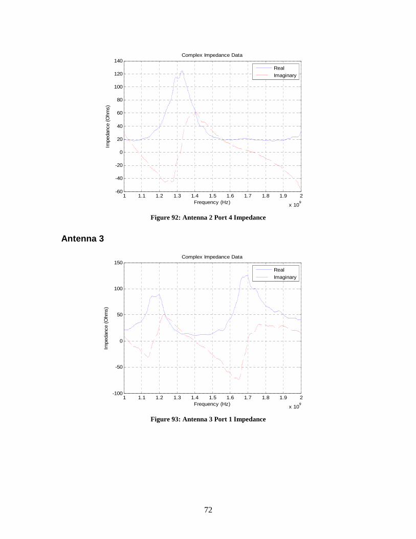
72
Figure 92: Antenna 2 Port 4 Impedance
Antenna 3
Figure 93: Antenna 3 Port 1 Impedance
1 1.1 1.2 1.3 1.4 1.5 1.6 1.7 1.8 1.9 2
x 109
-60
-40
-20
0
20
40
60
80
100
120
140Complex Impedance Data
Frequency (Hz)
Impe
danc
e (O
hms)
Real
Imaginary
1 1.1 1.2 1.3 1.4 1.5 1.6 1.7 1.8 1.9 2
x 109
-100
-50
0
50
100
150Complex Impedance Data
Frequency (Hz)
Impe
danc
e (O
hms)
Real
Imaginary

73
Figure 94: Antenna 3 Port 2 Impedance
Figure 95: Antenna 3 Port 3 Impedance
1 1.1 1.2 1.3 1.4 1.5 1.6 1.7 1.8 1.9 2
x 109
-100
-50
0
50
100
150
200Complex Impedance Data
Frequency (Hz)
Impe
danc
e (O
hms)
Real
Imaginary
1 1.1 1.2 1.3 1.4 1.5 1.6 1.7 1.8 1.9 2
x 109
-100
-50
0
50
100
150Complex Impedance Data
Frequency (Hz)
Impe
danc
e (O
hms)
Real
Imaginary

74
Figure 96: Antenna 3 Port 4 Impedance
Hybrids Taped to Ground Plane
Antenna 1
Figure 97: Antenna 1 S11 with Hybrids Taped to Ground plane
1 1.1 1.2 1.3 1.4 1.5 1.6 1.7 1.8 1.9 2
x 109
-60
-40
-20
0
20
40
60
80
100Complex Impedance Data
Frequency (Hz)
Impe
danc
e (O
hms)
Real
Imaginary
1 1.1 1.2 1.3 1.4 1.5 1.6 1.7 1.8 1.9 2
x 109
-25
-20
-15
-10
-5
0
5Return Loss Data
Frequency (Hz)
S11
(dB
)

75
Figure 98: Antenna 1 S11 Impedance with Hybrids Taped to Ground plane
Figure 99: Antenna 1 S22 with Hybrids Taped to Ground plane
1 1.1 1.2 1.3 1.4 1.5 1.6 1.7 1.8 1.9 2
x 109
-100
-50
0
50
100
150
200
250Complex Impedance Data
Frequency (Hz)
Impe
danc
e (O
hms)
Real
Imaginary
1 1.1 1.2 1.3 1.4 1.5 1.6 1.7 1.8 1.9 2
x 109
-16
-14
-12
-10
-8
-6
-4
-2
0
2Return Loss Data
Frequency (Hz)
S11
(dB
)

76
Figure 100: Antenna 1 S22 Impedance with Hybrids Taped to Ground plane
Antenna 2
Figure 101: Antenna 2 S11 with Hybrids Taped to Ground plane
1 1.1 1.2 1.3 1.4 1.5 1.6 1.7 1.8 1.9 2
x 109
-100
-50
0
50
100
150
200Complex Impedance Data
Frequency (Hz)
Impe
danc
e (O
hms)
Real
Imaginary
1 1.1 1.2 1.3 1.4 1.5 1.6 1.7 1.8 1.9 2
x 109
-20
-18
-16
-14
-12
-10
-8
-6
-4
-2
0Return Loss Data
Frequency (Hz)
S11
(dB
)
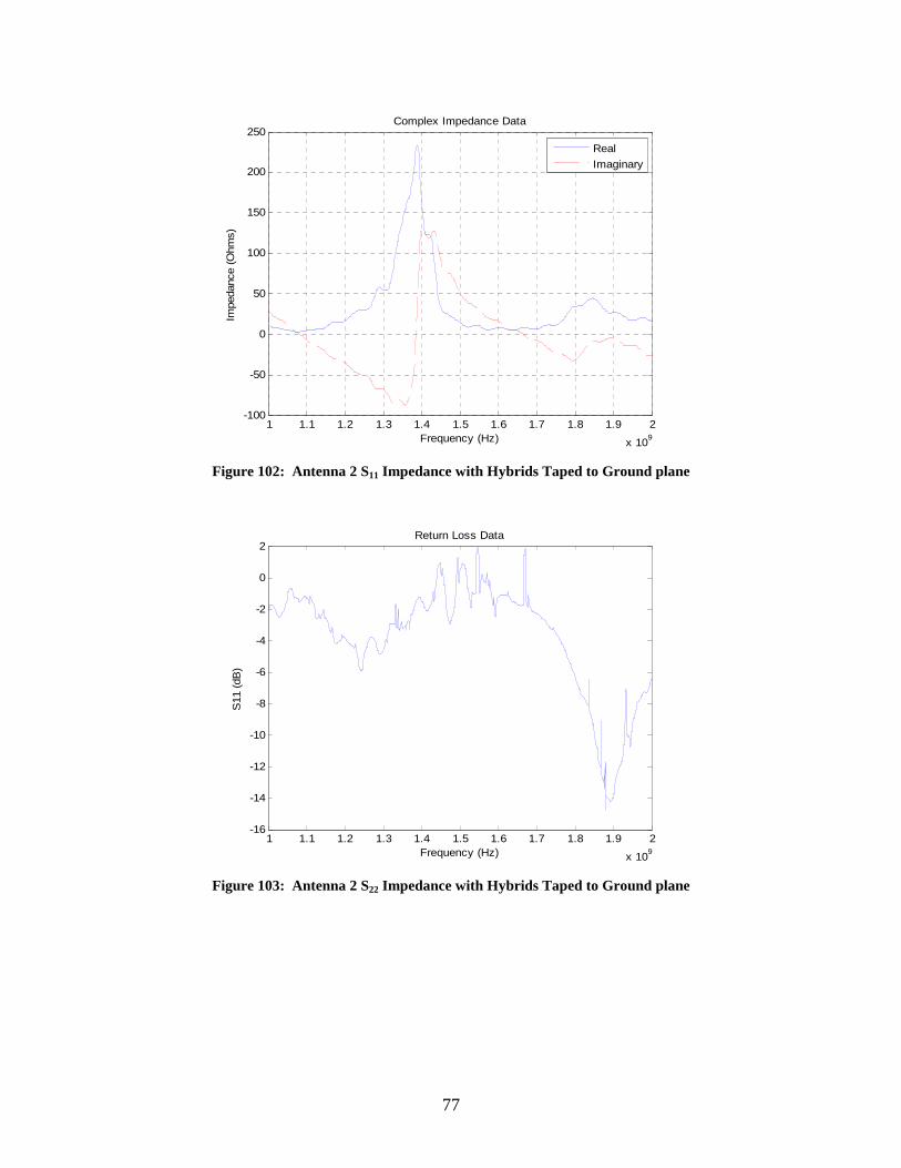
77
Figure 102: Antenna 2 S11 Impedance with Hybrids Taped to Ground plane
Figure 103: Antenna 2 S22 Impedance with Hybrids Taped to Ground plane
1 1.1 1.2 1.3 1.4 1.5 1.6 1.7 1.8 1.9 2
x 109
-100
-50
0
50
100
150
200
250Complex Impedance Data
Frequency (Hz)
Impe
danc
e (O
hms)
Real
Imaginary
1 1.1 1.2 1.3 1.4 1.5 1.6 1.7 1.8 1.9 2
x 109
-16
-14
-12
-10
-8
-6
-4
-2
0
2Return Loss Data
Frequency (Hz)
S11
(dB
)
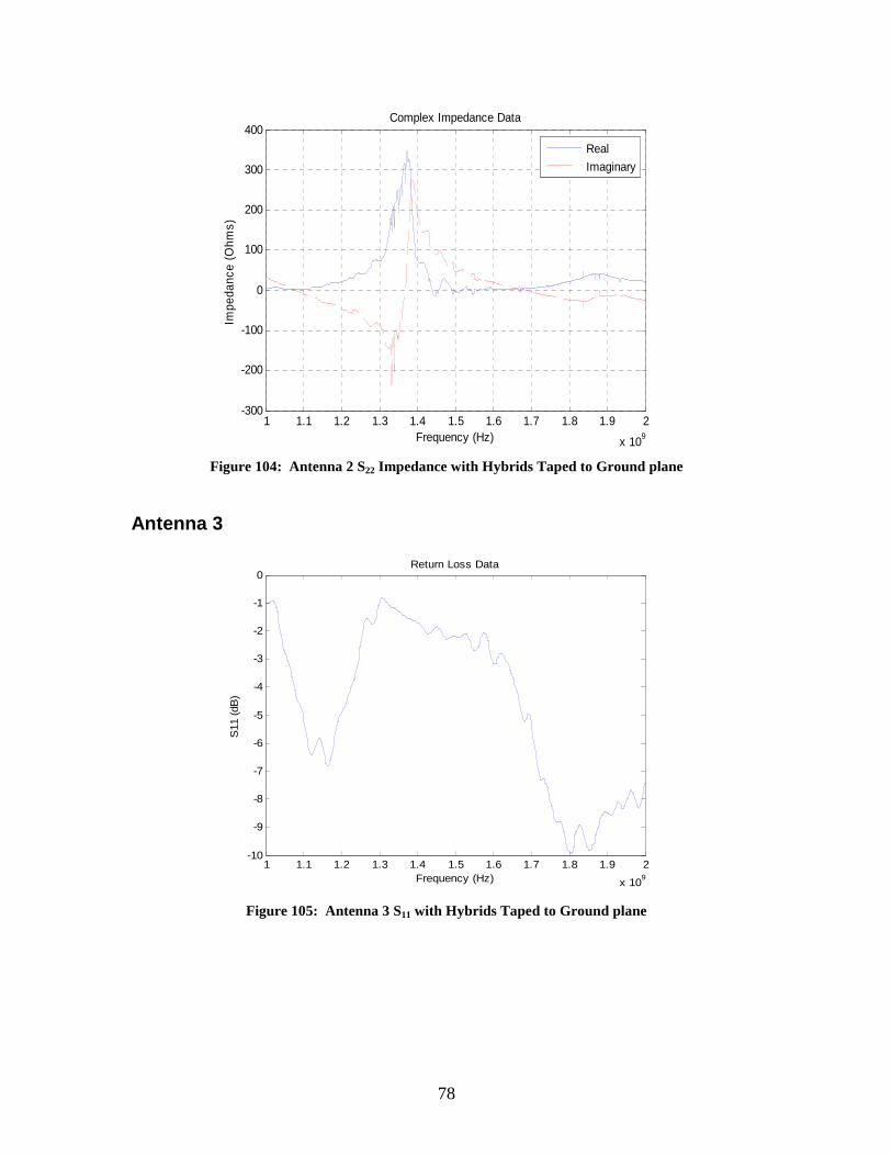
78
Figure 104: Antenna 2 S22 Impedance with Hybrids Taped to Ground plane
Antenna 3
Figure 105: Antenna 3 S11 with Hybrids Taped to Ground plane
1 1.1 1.2 1.3 1.4 1.5 1.6 1.7 1.8 1.9 2
x 109
-300
-200
-100
0
100
200
300
400Complex Impedance Data
Frequency (Hz)
Impe
danc
e (O
hms)
Real
Imaginary
1 1.1 1.2 1.3 1.4 1.5 1.6 1.7 1.8 1.9 2
x 109
-10
-9
-8
-7
-6
-5
-4
-3
-2
-1
0Return Loss Data
Frequency (Hz)
S11
(dB
)

79
Figure 106: Antenna 3 S11 Impedance with Hybrids Taped to Ground plane
Figure 107: Antenna 3 S22 with Hybrids Taped to Ground plane
1 1.1 1.2 1.3 1.4 1.5 1.6 1.7 1.8 1.9 2
x 109
-150
-100
-50
0
50
100
150
200
250
300Complex Impedance Data
Frequency (Hz)
Impe
danc
e (O
hms)
Real
Imaginary
1 1.1 1.2 1.3 1.4 1.5 1.6 1.7 1.8 1.9 2
x 109
-8
-7
-6
-5
-4
-3
-2
-1
0
1Return Loss Data
Frequency (Hz)
S11
(dB
)

80
Figure 108: Antenna 3 S22 Impedance with Hybrids Taped to Ground plane
1 1.1 1.2 1.3 1.4 1.5 1.6 1.7 1.8 1.9 2
x 109
-400
-300
-200
-100
0
100
200
300
400
500
600Complex Impedance Data
Frequency (Hz)
Impe
danc
e (O
hms)
Real
Imaginary

81
Appendix D: Testing Results of the Second Design
1.2 mm Center Conductor Antennas
Antenna 1
Figure 109: 1.2mm Center Conductor Antenna 1 S11
Figure 110: 1.2mm Center Conductor Antenna 1 S11 Impedance
1 1.1 1.2 1.3 1.4 1.5 1.6 1.7 1.8 1.9 2
x 109
-12
-11
-10
-9
-8
-7
-6
-5
-4
-3
-2Return Loss Data
Frequency (Hz)
S11
(dB
)
1 1.1 1.2 1.3 1.4 1.5 1.6 1.7 1.8 1.9 2
x 109
-200
-100
0
100
200
300
400Complex Impedance Data
Frequency (Hz)
Impe
danc
e (O
hms)
Real
Imaginary

82
Figure 111: 1.2mm Center Conductor Antenna 1 S22
Figure 112: 1.2mm Center Conductor Antenna 1 S22 Impedance
1 1.1 1.2 1.3 1.4 1.5 1.6 1.7 1.8 1.9 2
x 109
-14
-12
-10
-8
-6
-4
-2Return Loss Data
Frequency (Hz)
S11
(dB
)
1 1.1 1.2 1.3 1.4 1.5 1.6 1.7 1.8 1.9 2
x 109
-100
-50
0
50
100
150
200
250
300Complex Impedance Data
Frequency (Hz)
Impe
danc
e (O
hms)
Real
Imaginary

83
Figure 113: 1.2mm Center Conductor Antenna 1 S21
Figure 114: 1.2mm Center Conductor Antenna 1 S21 Impedance
1 1.1 1.2 1.3 1.4 1.5 1.6 1.7 1.8 1.9 2
x 109
-40
-35
-30
-25
-20
-15
-10Return Loss Data
Frequency (Hz)
S21
(dB
)
1 1.1 1.2 1.3 1.4 1.5 1.6 1.7 1.8 1.9 2
x 109
-40
-20
0
20
40
60
80Complex Impedance Data
Frequency (Hz)
Impe
danc
e (O
hms)
Real
Imaginary

84
Figure 115: Antenna 1 S21 Measured without Teflon or Wings
Figure 116: Antenna 1 S21 Impedance Measured without Teflon or Wings
1 1.1 1.2 1.3 1.4 1.5 1.6 1.7 1.8 1.9 2
x 109
-38
-36
-34
-32
-30
-28
-26
-24
-22
-20
-18Return Loss Data
Frequency (Hz)
S21
(dB
)
1 1.1 1.2 1.3 1.4 1.5 1.6 1.7 1.8 1.9 2
x 109
-10
0
10
20
30
40
50
60Complex Impedance Data
Frequency (Hz)
Impe
danc
e (O
hms)
Real
Imaginary

85
Figure 117: Antenna 1 S21 Measured with Teflon, without Wings
Figure 118: Antenna 1 S21 Impedance Measured with Teflon, without Wings
Antenna 2
1 1.1 1.2 1.3 1.4 1.5 1.6 1.7 1.8 1.9 2
x 109
-32
-30
-28
-26
-24
-22
-20
-18
-16
-14
-12Return Loss Data
Frequency (Hz)
S21
(dB
)
1 1.1 1.2 1.3 1.4 1.5 1.6 1.7 1.8 1.9 2
x 109
-40
-20
0
20
40
60
80Complex Impedance Data
Frequency (Hz)
Impe
danc
e (O
hms)
Real
Imaginary

86
Figure 119: Antenna 2 S21 Measured without Teflon or Wings
Figure 120: Antenna 2 S21 Impedance Measured without Teflon or Wings
1 1.1 1.2 1.3 1.4 1.5 1.6 1.7 1.8 1.9 2
x 109
-75
-70
-65
-60
-55
-50
-45
-40
-35
-30
-25Return Loss Data
Frequency (Hz)
S21
(dB
)
1 1.1 1.2 1.3 1.4 1.5 1.6 1.7 1.8 1.9 2
x 109
-10
0
10
20
30
40
50
60Complex Impedance Data
Frequency (Hz)
Impe
danc
e (O
hms)
Real
Imaginary

87
Figure 121: First Trial Antenna 2 S21 Measured with Teflon, without Wings
Figure 122: First Trial Antenna 2 S21 Impedance Measured with Teflon, without Wings
1 1.1 1.2 1.3 1.4 1.5 1.6 1.7 1.8 1.9 2
x 109
-45
-40
-35
-30
-25
-20
-15Return Loss Data
Frequency (Hz)
S21
(dB
)
1 1.1 1.2 1.3 1.4 1.5 1.6 1.7 1.8 1.9 2
x 109
-20
-10
0
10
20
30
40
50
60
70Complex Impedance Data
Frequency (Hz)
Impe
danc
e (O
hms)
Real
Imaginary
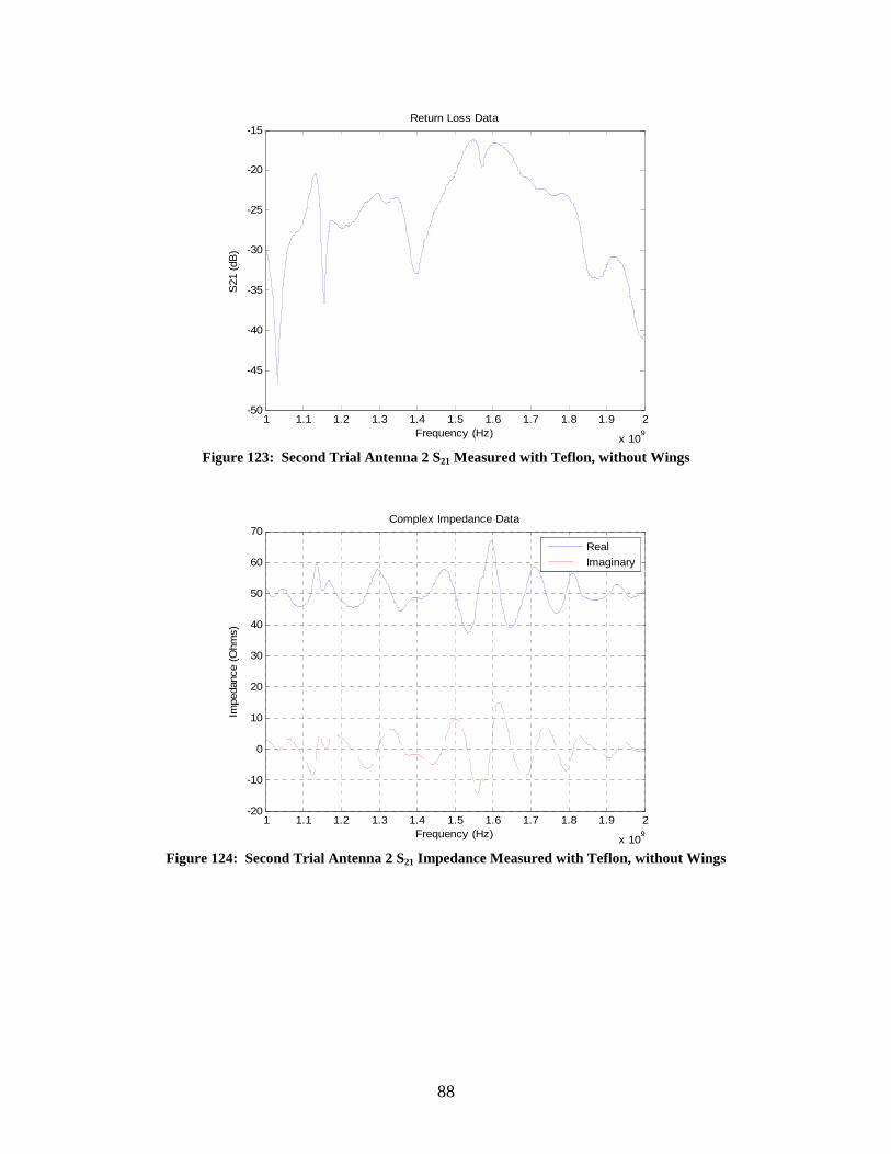
88
Figure 123: Second Trial Antenna 2 S21 Measured with Teflon, without Wings
Figure 124: Second Trial Antenna 2 S21 Impedance Measured with Teflon, without Wings
1 1.1 1.2 1.3 1.4 1.5 1.6 1.7 1.8 1.9 2
x 109
-50
-45
-40
-35
-30
-25
-20
-15Return Loss Data
Frequency (Hz)
S21
(dB
)
1 1.1 1.2 1.3 1.4 1.5 1.6 1.7 1.8 1.9 2
x 109
-20
-10
0
10
20
30
40
50
60
70Complex Impedance Data
Frequency (Hz)
Impe
danc
e (O
hms)
Real
Imaginary

89
2 mm Center Conductor Antenna
Figure 125: 2 mm Center Conductor Antenna S21 Measured with no Teflon or Wings
Figure 126: 2 mm Center Conductor Antenna S21 Impedance Measured with no Teflon or Wings
1 1.1 1.2 1.3 1.4 1.5 1.6 1.7 1.8 1.9 2
x 109
-31
-30
-29
-28
-27
-26
-25
-24
-23
-22
-21Return Loss Data
Frequency (Hz)
S21
(dB
)
1 1.1 1.2 1.3 1.4 1.5 1.6 1.7 1.8 1.9 2
x 109
-10
0
10
20
30
40
50
60Complex Impedance Data
Frequency (Hz)
Impe
danc
e (O
hms)
Real
Imaginary
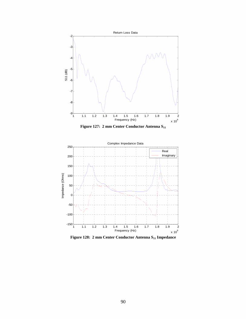
90
Figure 127: 2 mm Center Conductor Antenna S11
Figure 128: 2 mm Center Conductor Antenna S11 Impedance
1 1.1 1.2 1.3 1.4 1.5 1.6 1.7 1.8 1.9 2
x 109
-9
-8
-7
-6
-5
-4
-3
-2Return Loss Data
Frequency (Hz)
S11
(dB
)
1 1.1 1.2 1.3 1.4 1.5 1.6 1.7 1.8 1.9 2
x 109
-150
-100
-50
0
50
100
150
200
250Complex Impedance Data
Frequency (Hz)
Impe
danc
e (O
hms)
Real
Imaginary

91
Figure 129: 2 mm Center Conductor Antenna S22
Figure 130: 2 mm Center Conductor Antenna S22 Impedance
1 1.1 1.2 1.3 1.4 1.5 1.6 1.7 1.8 1.9 2
x 109
-45
-40
-35
-30
-25
-20
-15
-10
-5
0Return Loss Data
Frequency (Hz)
S11
(dB
)
1 1.1 1.2 1.3 1.4 1.5 1.6 1.7 1.8 1.9 2
x 109
-80
-60
-40
-20
0
20
40
60
80
100
120Complex Impedance Data
Frequency (Hz)
Impe
danc
e (O
hms)
Real
Imaginary

92
Figure 131: 2 mm Center Conductor Antenna S21
Figure 132: 2 mm Center Conductor Antenna S21 Impedance
3 mm Center Conductor Antenna
1 1.1 1.2 1.3 1.4 1.5 1.6 1.7 1.8 1.9 2
x 109
-60
-55
-50
-45
-40
-35
-30
-25Return Loss Data
Frequency (Hz)
S21
(dB
)
1 1.1 1.2 1.3 1.4 1.5 1.6 1.7 1.8 1.9 2
x 109
-10
0
10
20
30
40
50
60Complex Impedance Data
Frequency (Hz)
Impe
danc
e (O
hms)
Real
Imaginary

93
Figure 133: 3 mm Center Conductor Antenna S11
Figure 134: 3 mm Center Conductor Antenna S22

94
Figure 135: 3 mm Center Conductor Antenna S21
Figure 136: 3 mm Center Conductor Antenna S11 with 90º Hybrid

95
References
[1] "GPS Tutorial". Trimble. 14April, 2008 <http://www.trimble.com/gps/whygps.shtml>.
[2] Kaswarra, Bernard, and Quddus, Wasim. ""Iris" - A Broadband Base Station GPS Antenna with a Single Balun". March 2007:
[3] McIntyre, Melville D.. "Inertially augmented GPS landing system". European Patent Office - Boeing Company. 12 April 2008 <https://publications.european-patent-office.org/PublicationServer/documentpdf.jsp?iDocId=5201693&iebug=.pdf>.
[4] " Polar Services - Summit Camp GPS System - Base Station". UNAVCO. 15 April 2008 <http://facility.unavco.org/project_support/polar/summit/base.html>.
[5] "Circular polarization". Wikipedia. 13 April 2008 <http://en.wikipedia.org/wiki/Circular_polarization>.
[6] "Choke Ring Theory". Javad Navigation Systems. 15 April 2008 <http://www.javad.com/jns/index.html?/jns/technology/Choke%20Ring%20Theory.html>.
[7] Ansoft HFSS, User's Guide - High Frequency Structure Simulator. Pittsburg: Ansoft Corporation, 2003.
[8] Ludwig, Reinhold, and Pavel Bretchko. RF Circuit Design. Upper Saddle River, NJ: Prentice Hall, 2000.
[9] Kraus, John D., Ronald J. Marhefka, and Ahmad S. Khan. Antennas for all Applications. New Delhi: McGraw-Hill, 2006.
[10] "Permanent GPS Stations - Choke Ring Antenna Calibrations". UNAVCO. 14 April, 2008 <http://facility.unavco.org/project_support/permanent/equipment/antennas/ant_cals.html>.
[11] Puzella, Angelo, Li, Tao, and Makarov, Sergey N. "A Quad-Line Vertical Balun Column for the Use with a Dyson Balun and a Turnstile Radiator ". 2008:
[12] Pozar, David M. Microwave Engineering, 3rd ed. New York: Wiley, 2005.


![Frequency[GHz] 0.8 1.2 1.4 -10 -20 o E -30 40 1.6 - S41 ...](https://static.fdocuments.in/doc/165x107/6175a200f2a28a2054196e17/frequencyghz-08-12-14-10-20-o-e-30-40-16-s41-.jpg)
![Automated Design Strategy for High Performance Mixed ...€¦ · IL-PLL DMDLL DPLL MDLL IL-PLL Freq. [GHz] 1.2 (0.5-1.6) 1.5 (0.8-1.8) 1.5 (0.8-1.8) 1.6 0.216 Ref. [MHz] 300 (40-300)](https://static.fdocuments.in/doc/165x107/60d300bb6a843e51fd2d6423/automated-design-strategy-for-high-performance-mixed-il-pll-dmdll-dpll-mdll.jpg)