A COMPUTATIONAL STUDY OF SURFACE ADSORPTION AND …
168
A COMPUTATIONAL STUDY OF SURFACE ADSORPTION AND DESORPTION By LIN-LIN WANG A DISSERTATION PRESENTED TO THE GRADUATE SCHOOL OF THE UNIVERSITY OF FLORIDA IN PARTIAL FULFILLMENT OF THE REQUIREMENTS FOR THE DEGREE OF DOCTOR OF PHILOSOPHY UNIVERSITY OF FLORIDA 2004
Transcript of A COMPUTATIONAL STUDY OF SURFACE ADSORPTION AND …

A COMPUTATIONAL STUDY OF SURFACE ADSORPTION AND DESORPTION
By
LIN-LIN WANG
A DISSERTATION PRESENTED TO THE GRADUATE SCHOOL OF THE UNIVERSITY OF FLORIDA IN PARTIAL FULFILLMENT
OF THE REQUIREMENTS FOR THE DEGREE OF DOCTOR OF PHILOSOPHY
UNIVERSITY OF FLORIDA
2004

Copyright 2004
by
Lin-Lin Wang

To my parents.

ACKNOWLEDGMENTS
I have benefited from numerous people and many facilities during my graduate
study at the University of Florida. First, I would like to acknowledge my advisor,
Professor Hai-Ping Cheng, whose enthusiasm and expertise were greatly appreciated. I
would also like to thank Professors James W. Dufty, Arthur F. Hebard, Jeffery L. Krause
and Samuel B. Trickey for serving on my supervisory committee.
I am very grateful for many current and former members of the Quantum Theory
Project for their support. Of special note are Dr. Ajith Perera, Dr. Magnus Hedström, and
Dr. Andrew Kolchin. I spent a wonderful student life in the University of Florida with
numerous friends. They are Dr. Mao-Hua Du, Mr. Chun Zhang, Dr. Rong-Liang Liu, Dr.
Lin-Lin Qiu, Dr. Zhi-Hong Chen, Mr. Xu Du, Mr. Ling-Yin Zhu, Mr. Wu-Ming Zhu, Mr.
Chun-Lin Wang and many others. At last, I would like to thank my loving parents, Xue-
Ping Li and Xiang-Jin Wang, and my beautiful wife, Dr. Yi Wu, for their endless support.
This work has been supported by DOE/Basic Energy Science/Computational
Material Science under contract number DE-FG02-97ER45660
.
iv

TABLE OF CONTENTS page ACKNOWLEDGMENTS ................................................................................................. iv
LIST OF TABLES............................................................................................................ vii
LIST OF FIGURES ......................................................................................................... viii
ABSTRACT....................................................................................................................... xi
CHAPTER 1 OVERVIEW.................................................................................................................1
2 DENSITY FUNCTIONAL STUDY OF THE ADSORPTION OF A C60 MONOLAYER ON NOBLE METAL (111) SURFACES..........................................6
2.1 Introduction.............................................................................................................6 2.2 Theory, Method, and Computational Details .......................................................11
2.2.1 DFT Formulism with a Plane Wave Basis Set ...........................................11 2.2.2 Computational Details ................................................................................14
2.3 Results and Discussion .........................................................................................16 2.3.1 Adsorption of a C60 ML on Cu(111) Surface .............................................16
2.3.1.1 Energetics and Adsorption Geometries............................................16 2.3.1.2 Electronic Structures ........................................................................19 2.3.1.3 Electron Density Redistribution and Work Function Change..........24
2.3.2 Adsorption of a C60 ML on Ag (111) and Au(111) Surfaces .....................30 2.3.2.1 Energetics and Adsorption Geometries............................................30 2.3.2.2 Electronic Structure and Bonding Mechanism.................................34 2.3.2.3 Work Function Change ....................................................................40 2.3.2.4 Simulated STM Images ....................................................................45 2.3.2.5 Difference in Band Hybridization ....................................................47
2.3.3 Adsorption of C60 ML on Al(111) and Other Surfaces ..............................48 2.3.4 Adsorption of SWCNT on Au(111) Surface ..............................................51
2.4 Conclusion ............................................................................................................57 3 MOLECULAR DYNAMICS SIMULATION OF POTENTIAL SPUTTERING ON
LiF SURFACE BY SLOW HIGHLY CHARGED IONS..........................................59
3.1 Introduction...........................................................................................................59
v

3.2 Modeling and Simulation ....................................................................................62 3.2.1 Calculations of Potential Energy Functions ...............................................64 3.2.2 Two-body Potentials for MD Simulation ...................................................71 3.2.3 Simulation Details ......................................................................................75
3.3 Results and Discussion ........................................................................................76 3.3.1 Initial Condition..........................................................................................76 3.3.2 Surface Modification ..................................................................................77 3.3.3 Sputtering Yield..........................................................................................80 3.3.4 Profile of Dynamics....................................................................................85
3.4 Conclusion ...........................................................................................................89 4 AN EMBEDDING ATOM-JELLIUM MODEL........................................................90
4.1 Introduction...........................................................................................................90 4.2 DFT Formulism for Embedding Atom-jellium Model.........................................92 4.3 Results and Discussion .........................................................................................95
5 FRACTURE AND AMORPHIZATION IN SiO2 NANOWIRE STUDIED BY A
COMBINED MD/FE METHOD................................................................................98
5.1 Introduction...........................................................................................................98 5.2 Methodology.......................................................................................................100
5.2.1 Summary of Finite Element Method ........................................................100 5.2.2 Hybrid MD/FE: New Gradual Coupling ..................................................104
5.3 Results.................................................................................................................106 5.3.1 Interface Test ............................................................................................107 5.3.2 Stretch Simulation ....................................................................................110
6 SUMMARY AND CONCLUSIONS.......................................................................113
APPENDIX A TOTAL ENERGY CALCULATION OF SYSTEM WITH PERIODIC
BOUNDARY CONDITIONS ..................................................................................115
B REVIEW OF DEVELOPMENT IN FIRST-PRINCIPLES PSEUDOPOTENTIAL125
B.1 Norm-Conserving Pseudopotential ....................................................................125 B.2 Ultrasoft Pseudopotential and PAW ..................................................................131
LIST OF REFERENCES.................................................................................................143
BIOGRAPHICAL SKETCH ...........................................................................................156
vi

LIST OF TABLES
Table page 2-1. Structural and energetic data of an isolated C60 molecule..........................................15
2-2. Structural and energetic data for bulk Cu, Ag, Au, clean Cu(111), Ag(111) and Au(111) surfaces. .....................................................................................................15
2-3. Work function change of a C60 ML adsorbed on a Cu(111) surface..........................28
2-4. Adsorption energies of a C60 ML on Ag(111) and Au(111) surfaces ........................31
2-5. The relaxed structure of a C60 ML adsorbed on Ag(111) and Au(111) surfaces with its lowest energy configuration. ...............................................................................33
2-6. Work function change of a C60 ML adsorbed on Cu(111), Ag(111) and Au(111) surfaces.....................................................................................................................41
3-1. Sputtering yields of ten MD simulations with different initial conditions. ................83
vii

LIST OF FIGURES
Figure page 2-1. Surface geometry and adsorption sites for a C60 ML on a Cu(111) surface...............17
2-2. Adsorption energies as functions of rotational angle for a C60 ML on a Cu(111) surface. .....................................................................................................................18
2-3. Total density of states and partial DOS projected on the C60 ML and the Cu(111) surface. .....................................................................................................................19
2-4. Band structure for the adsorption of a C60 ML on a Cu(111) surface. .......................20
2-5. DOS of an C60 ML before and after its adsorption on a Cu(111) surface. .................21
2-6. Partial DOS of different adsorption configurations for a C60 ML on a Cu(111) surface. .....................................................................................................................23
2-7. Iso-surfaces of electron density difference for a C60 ML on a Cu(111) surface.. ......25
2-8. Planar averaged electron density differences and the change in surface dipole moment for the adsorption of a C60 ML on a Cu(111) surface. ...............................26
2-9. Work function change and electronic charge transfer as functions of the distance between a C60 ML and a Cu(111) surface. ...............................................................29
2-10. Surface geometry and adsorption sites for a C60 ML on Ag(111) and Au(111) surfaces.....................................................................................................................31
2-11. Adsorption energies as functions of rotational angle of C60 ML on Ag(111) and Au(111) surfaces. .....................................................................................................32
2-12. Density of states of a C60 ML on Ag(111) and Au(111) surfaces. ...........................35
2-13. Iso-surfaces of electron density difference for the adsorption of a C60 ML on Ag(111) and Au(111) surfaces. ................................................................................36
2-14. Partial DOS of different adsorption configurations for a C60 ML on Ag(111) and Au(111) surfaces. .....................................................................................................39
2-15. Planar averaged electron density differences and the change in surface dipole moment of a C60 ML on Ag(111) and Au(111) surfaces. ........................................42
viii

2-16. Work function change and electronic charge transfer as functions of the distance between the C60 and the metal surfaces....................................................................45
2-17. Simulated STM images of a C60 ML on Ag(111) and Au(111) surfaces. ................46
2-18. Difference in electronic structures for the adsorption of a C60 ML on noble metal (111) surfaces. ..........................................................................................................47
2-19. Density of states for the adsorption of a C60 ML on a Al(111) surface....................49
2-20. Electron density difference and change in surface dipole moment for a C60 ML on a Al(111)surface..........................................................................................................50
2-21. Density of states for the adsorption of a (5,5) SWCNT on a Au(111) surface. .......54
2-22. Electron density difference and change in surface dipole moment for a (5,5) SWCNT on a Au(111)surface. .................................................................................55
2-23. Density of states for the adsorption of a (8,0) SWCNT on a Au(111) surface. .......56
2-24. Electron density difference and change in surface dipole moment for a (8,0) SWCNT on a Au(111)surface. .................................................................................56
3-1. Calculated ground state potential energy function for (Li+Li+) from CCSD[T]. .......64
3-2. Calculated ground state potential energy function for (F−F−) from CCSD[T]. ..........65
3-3. Calculated potential energy functions for (Li+F−) and (Li0F0) from CCSD[T]. .........66
3-4. Calculated potential energy functions for (Li+Li0) from CCSD[T]............................67
3-5. Calculated potential energy functions for (Li0F−) from CCSD[T]. ............................67
3-6. Calculated potential energy functions for (Li0Li0) from CCSD[T]. ...........................68
3-7. Calculated potential energy functions for (Li+F0) from CCSD[T]. ............................68
3-8. Calculated potential energy functions for (F0F−) from CCSD[T]. .............................69
3-9. Calculated potential energy functions for (F0F0) from CCSD[T]...............................69
3-10. Potential energy functions for ground state (Li+F−). ................................................71
3-11. Four sets of potential energy functions for each species in LiF surface used in the MD simulations. .......................................................................................................73
3-12. Snapshot of the LiF surface at t 0= for simulation 6. .............................................75
3-13. Snapshot of the LiF surface at t 1.2= ps for simulation 6. ......................................77
ix

3-14. Snapshot of the the LiF surface at t 1.2= ps for simulation 9. ................................78
3-15. Distribution functions of the number of particles and potential energy along the z direction at t ps for simulation 6.....................................................................79 1.2=
3-16. Distribution functions of the kinetic energy along the z direction at ps for simulation 6. .............................................................................................................84
1.2t =
3-17. Normalized angular distribution functions of the neutral particles averaged over simulations 3, 6, 7, and 8 at t 1.2= ps. ....................................................................85
3-18. Distribution functions of the number of particles and potential energy along the z direction of Li0 at different time instants for simulation 6. ......................................86
3-19. Distribution functions of the number of particles and potential energy along the z direction of F0 at different times for simulation 6. ...................................................87
4-1. A jellium surface modeled by a seven-layer Al slab with 21 electrons. ....................95
4-2. The quantum size effect of jellium surfaces, (a) Al and (b) Cu. ................................96
4-3. Partial density of states projected on atomic orbitals. ...............................................97
5-1. Geometry of the α-cristobalite (SiO2) nanowire.......................................................107
5-2. Energy conservation test with respect to time for (a) FE only, (b) MD only, and (c) both FE and MD.....................................................................................................108
5-3. Distributions of force and velocity in the y direction during a pulse propagation test for the MD/FE interface. ........................................................................................109
5-4. The stress-strain relation for a uniaxial stretch applied in the y direction of the nanowire at speed of 0.035 1ps− . ...........................................................................110
5-5. Five snapshots from the tensile stretch applied in the y direction of the nanowire at speed of 0.035 ps . ...............................................................................................111 1−
5-6. Pair correlation functions of the nanowire during the uniaxial stretch simulation...112
x

Abstract of Dissertation Presented to the Graduate School of the University of Florida in Partial Fulfillment of the Requirements for the Degree of Doctor of Philosophy
A COMPUTATIONAL STUDY OF SURFACE ADSORPTION AND DESORPTION
By
Lin-Lin Wang
May 2004
Chair: Hai-Ping Cheng Major Department: Physics
In this work, the phenomena of surface adsorption and desorption have been
studied by various computational methods. Large-scale density functional calculations
with the local density approximation have been applied to investigate the energetics and
electronic structure of a C60 monolayer adsorbed on noble metal (111) surfaces. In all
cases, the most energetically preferred adsorption configuration corresponds to a hexagon
of C60 adsorbing on an hcp site. A small amount of electronic charge transfer of 0.8, 0.5
and 0.2 electrons per molecule from the Cu(111), Ag(111) and Au(111) surfaces to C60
has been found. We also find that the work function decreases by 0.1 eV on Cu(111)
surface, increases by 0.1 eV on Ag(111) surface and decreases by 0.6 eV on Au(111)
surface upon the adsorption of a C60 monolayer. The puzzling work function change is
well explained by a close examination of the surface dipole formation due to electron
density redistribution in the interface region.
Potential sputtering on the lithium fluoride (LiF) (100) surface by slow highly
charged ions has been studied via molecular dynamics (MD) simulations. A model that is
xi
different from the conventional MD is formulated to allow electrons to be in the ground
state as well as the low-lying excited states. The interatomic potential energy functions
are obtained by a high-level quantum chemistry method. The results from MD
simulations demonstrate that the so-called defect-mediated sputtering model provides a
qualitatively correct picture. The simulations provide quantitative descriptions in which
neutral particles dominate the sputtering yield by 99%, in agreement with experiments.
An embedding atom-jellium model has been formulated into a multiscale
simulation scheme to treat only the top metal surface layers in atomistic pseudopotential
and the rest of the surface in a jellium model. The calculated work functions of Al and Cu
clean surfaces agree well with the all-atomistic calculations. The multiscale scheme of
combining finite element (FE) and MD methods is also studied. A gradual coupling of
the FE and MD in the interface region is proposed and implemented, which shows
promising results in the simulation of the breaking of a SiO2 nanowire by tensile stretch.
xii
CHAPTER 1 OVERVIEW
The importance of understanding surface phenomena stems from the fact that for
many physical and chemical phenomena, a surface plays a key role. A better
understanding and, ultimately, a predictive description of surface and interface properties
is vital for the progress of modern technology, such as catalysis, miniaturization of
electronic circuits, and emerging nanotechnology.
The richness of physical and chemical properties of surfaces finds its fundamental
explanation in the arrangement of atoms, the distribution of electrons, and their response
to external perturbations. For examples, the processes of surface adsorption and
desorption are the results of the interplay between geometric structure and electronic
structure of the adsorbate and substrate. The ground state electronic structure fully
determines the equilibrium geometry of the adsorption system. The ground state
electronic structure also largely determines the chemical reaction and dynamics on the
surface, such as transition states and reaction barriers. Nevertheless, more severe
processes of surface dynamics, such as surface desorption stimulated by external laser
fields, electron and charged ion bombardments, always involve electronic excited states
and energy exchange between electronic and ionic degree of freedom. To study these
processes, the electronic structure of excited states must be included.
Computer simulation has been proved to be a powerful tool, besides experiment
and theory, to study surface science in recent decades. There are two categories of
simulation, which are characterized by the degrees of freedom they consider and the
1

2
implemented scales. One is molecular dynamics (MD) [1], which treats atoms and
molecules as classical particles and omits the degrees of freedom from the electrons. The
other is quantum mechanical methods, which treats electrons explicitly. Although the two
kinds of simulation are different, they are strongly connected and compose a hierarchy of
knowledge of the system studied. In MD, classical particles move according to the
coupled Newton’s equations in force fields. Although no electron is included in such
simulations, the force fields have input in principle from electronic information. In
quantum mechanical methods, the Schrödinger equation is solved to include the many-
body interaction among electrons explicitly. Once the electronic structure is known, the
total energy of the system can be calculated. Molecule dynamics can be done with the
force calculated from first-principles.
To solve a many-body Schrödinger equation, two categories of methods are
available. Traditionally, in quantum chemistry [2], wave-function-based methods are
pursued, such as the Hartree-Fock method, which only treats the exchange effect of
electrons explicitly. The omitted correlation effect of electrons is included by many post
Hartree-Fock methods, such as configuration interaction (CI) and various orders of many-
body perturbation theory (MBPT). The coupled-cluster method is closely related, in that
the correlation effect of electrons can be improved systematically by considering the
single, double, triple, etc, excitations.
Recently, the electron-density based method, i.e., density functional theory
(DFT) [3, 4], has become popular because it can reach intermediate accuracy, comparable
to single CI, at relatively low computational cost. According to the Hohenberg-Kohn
theorem [5, 6], the ground state total energy of an electronic system is a unique functional

3
of the electron density. The exchange-correlation (XC) energy from the many-body
effects can be treated as a functional of electron density. Thus, DFT in the Kohn-Sham
approach maps the many-body problem for interacting electrons into a set of one-body
equations for non-interacting electrons subjected to an effective potential. The proof of
the Hohenberg-Kohn-Sham theorems and related development of XC functional of
electrons are not the focus of this work. The remaining one-particle Kohn-Sham (KS)
equation still poses a substantial numerical challenge. Among the various strategies,
plane wave basis sets with pseudopotentials stands out as a popular choice because of its
efficiency. In the past decade, new developments in pseudopotential formalism, more
efficient algorithm in iterative minimization, and faster computer hardware have made
large-scale, first-principles DFT simulation treating hundreds of atoms a reality.
In this dissertation, we use all of these methods to study the phenomenon of surface
adsorption and desorption. In Chapter 2, the ground state properties of a C60 monolayer
(ML) adsorbed on noble metal (Cu, Ag and Au) (111) surfaces are studied by large-scale
DFT calculations. The adsorption energetics, such as the lowest energy configuration,
translational and rotational barriers are obtained. Electronic structure information, such as
density of states, charge transfer, and electron density redistribution, are also studied.
With the detailed information on electronic structure, we explain very well the opposite
change of work function on Cu and Au surfaces vs. Ag surface, which has been a
puzzling phenomenon observed in experiments.
In Chapter 3, we study a surface dynamical process, the response of a LiF(100)
surface to the impact of highly charged ions (HCI) via MD simulation. We extend the
conventional MD formalism to include the forces from electronic excited states

4
calculated by a high-level quantum chemistry method. Within this new model, the so-
called potential sputtering mechanism is examined by MD simulations. Our results agree
well with the experimental results on the sputtering pattern and the observation of
dominant sputtering yield in neutral particles. We found that the potential sputtering
mechanism can be well-explained by the two-body potential energy functions from the
electronic excited states.
We will also address the issues of multiscale simulation in Chapter 4 and 5. There
are two major reasons for multiscale simulations. One is the compromise between
accuracy and efficiency. Only a crucial central region needs to be treated in high accurate
method; the surrounding region can be treated in less accurate, but more computationally
tractable approximation. In Chapter 4, we consider using jellium model as a simplified
pseudopotential together with the atomistic pseudopotential to study the properties of
metal surfaces in DFT calculation. The other reason to do multiscale simulation, which is
more important, is that some phenomena in nature are intrinsically scale-coupled in
different time, length and energy scales. For less scale-coupled phenomena, a sequential
multiscale scheme usually works fine. One such example is the potential sputtering on
LiF surface by HCI studied in Chapter 2. In that study, first, a highly accurate quantum
chemistry method is used to calculate the potential energy functions. Then this
information is fed to the MD simulation to study the dynamical processes. For strongly
scale-coupled phenomena, only an intrinsic multiscale model can capture all the relevant
physical processes, for example, material failure and crack propagation. The stress field,
plastic deformation around the crack tip, and bond breaking inside the crack tip all
depend on each other. These three different length scales are coupled strongly. In Chapter

5
5, we construct a combined finite element and molecule dynamics method to investigate
the breaking of a SiO2 nanowire.

CHAPTER 2 DENSITY FUNCTIONAL STUDY OF THE ADSORPTION OF A C60 MONOLAYER
ON NOBLE METAL (111) SURFACES
2.1 Introduction
Ever since its discovery [7], C60 has attracted much research attention because of its
extraordinary physical properties and potential application in nanotechnology. The
adsorption of the C60 molecule on noble metal surfaces has been studied intensively in
experiments over the last decade [8]. Due to the high electron affinity of the C60 molecule
as well as the metallic nature of the surfaces, the interaction has been understood in terms
of electronic charge transfer from noble metal surfaces to the adsorbed C60 monolayer
(ML). According to the conventional surface dipole theory, all noble metal surfaces
should have an increase in work function upon the adsorption of a C60 ML. However, a
small decrease in work function on Cu surfaces [9] and Au surfaces [10], and a small
increase in work function on Ag surfaces [11] have been observed in experiments with
the adsorption of a C60 ML. Electronic charge transfer alone can not explain this
phenomenon [9, 10, 12]. Furthermore, the most preferred adsorption site and orientation
of the C60 ML on Ag(111) and Au(111) surfaces are still unclear [13-16]. All these basic
issues require additional insight to understand the fundamental nature of the interaction.
Evidence for electronic charge transfer from noble metal (111) surfaces to C60 has
been observed in various experiments. The C60-Cu film is a system in which fascinating
phenomena have been observed in studies of conductance as a function of the thickness
of Cu film [17]. Experiments indicate that when a C60 monolayer is placed on top of a
6

7
very thin Cu film, the resistance of the monolayer is measured about 8000 Ω, which leads
to resistivity corresponding to half of the three-dimensional alkali-metal-doped
compounds A3C60 (A=K, Rb). When the C60 is beneath the Cu film, the ML also
enhances the conductance. It is suggested from experimental analysis that the
enhancement of conductance in the C60-Cu systems is due to charge transfer from Cu to
C60 at the interface. Further experimental measurements indicate that when the thickness
of the Cu film increases, the resistance curves cross. As the thickness of the Cu film
increases, the conductance of the film increases to approach the bulk Cu limit, which is
much higher than the conductance of the electron-doped C60. When the thick Cu film is
covered with a C60-ML, the resistance of the system is increased. This effect is
understood as a result of the diffusive surface scattering process.
More direct evidence for electronic charge transfer from noble metal (111) surfaces
to an adsorbed C60 monolayer come from photon emission spectroscopy (PES). In
valence band PES [9, 10, 18-25], a small peak appears just below the Fermi level due to
the lowest unoccupied molecule orbital (LUMO) derived bands of the C60, which cross
the Fermi level and are partially filled upon adsorption. In carbon 1s core level PES [9,
10, 18, 19, 21, 24, 26], the binding energy shifts toward lower energy and the line shape
becomes highly asymmetric due to the charge transfer. Modification in the electronic
structure of the molecules is also found to be responsible for the enhancement in Raman
spectroscopy [19, 27-31]. A substantial shift of the Ag(2) pentagonal pinch mode to lower
frequency for C60 molecule adsorbed on noble metal surfaces has a pattern similar to that
from the alkali metal doped C60 compound.
8
In regard to the magnitude of electronic charge transfer from noble metal surfaces
to an adsorbed C60 monolayer, different techniques give different results. By comparing
the size of the shift of the Ag(2) mode in Raman spectroscopy between C60 adsorbed on
polycrystalline noble metal surfaces and that for K3C60, a charge transfer of less than
three electrons per molecule can be derived [19]. In valence PES studies, the intensity of
the C60 LUMO-derived bands is compared to the intensity of the C60 HOMO-derived
bands or the intensity of the C60 LUMO-derived bands co-adsorbed with alkali metals.
These studies indicate that 1.6, 0.75 and 0.8 electrons per molecule are transferred from
Cu(111) [10], Ag(111) [22] and Au(111) [10] surfaces to the C60 monolayer. Another
study shows that 1.8, 1.7 and 1.0 electrons per molecule are transferred from
polycrystalline Cu, Ag and Au surfaces, respectively, to the C60 monolayer [20]. Based
on the observed electronic charge transfer, the interaction between the C60 and the noble
metal surfaces is assigned as ionic in nature.
The geometry of an adsorbed C60 monolayer on noble metal (111) surfaces has
been studied in numerous STM experiments [13-16, 32-42] as well as by x-ray diffraction
experiments [43-46]. At the beginning of the adsorption on these surfaces, C60 is mobile
on the terrace and occupies initially the step sites to form a closely packed pattern. After
the first monolayer is complete, C60 forms a commensurate hexagonal (4×4) structure on
the Cu(111) surface. On the Ag(111) surface, C60 forms a commensurate hexagonal
( 2 3 2 3× )R30o structure, and some additional structures rotated by 14o or 46o from the
foregoing structure [16]. Then after annealing, only the ( 2 3 2 3× )R30o structure
remains, which indicates that this is the most energetically favored structure. On the
Au(111) surface, the adsorption configuration is more complicated, due to reconstruction

9
of the free Au(111) surface. In addition to the commensurate hexagonal
( 2 3 2 3× )R30o structure and the rotated structures, C60 can also form a (38×38) in-
plane structure [13-15, 36, 37]. After annealing, only the well-ordered ( 2 3 2 3× )R30o
structure remains. The reconstruction of the free Au(111) surface is lifted. Recently,
another commensurate close-packed (7×7) structure was proposed [39].
Considering the adsorption site and the orientation of the C60 monolayer in the
(4×4) structure on the Cu(111) surface, the Sakurai group [33] found that C60 adsorbs on
a threefold hollow site with a hexagon parallel to the surface. They observed clearly a
threefold symmetric STM image of C60 with a ring shape and a three-leaf shape for
negative and positive bias respectively. So it must be a hexagon of C60 parallel to the
Cu(111) surface. With this orientation, because of the nonequivalent 60o rotation, there
should be only two domains in the well-ordered (4×4) structure if C60 occupies the on-top
site. Their observation shows four domains, which indicates that C60 occupies the
threefold hollow sites, both hcp and fcc sites. For the ( 2 3 2 3× )R30o structure of C60
on the Ag(111) and Au(111) surfaces, Altman and Colton [13-15] proposed, on the basis
of experimental STM images, that the adsorption configuration is a pentagon of C60 on an
on-top site for both surfaces. However, Sakurai et al. [16], again based on interpretations
of experimental STM images, proposed that the adsorption site is the threefold hollow
site for the Ag(111) surface, in analogy to the (4×4) structure of C60 monolayer adsorbed
on the Cu(111) surface [33]. But they did not specify the orientation of the C60 molecules
on the Ag(111) surface.
Despite the large amount of experimental data on electronic, transport, and optical
properties, many basic issues remain unanswered. Although electronic charge transfer

10
from the noble metal substrates to the C60 over-layer is evident, the work function
actually decreases on the Cu(111) surface by 0.08 eV [9], decreases on the Au(111)
surface by 0.6 eV [10], and increases on the Ag(110) surface by 0.4 eV [11], which
cannot be understood at all within the simple description of surface dipole layer
formation due to charge transfer that is ionic in nature. Furthermore, the adsorption site
and orientation of the C60 monolayer on Ag(111) and Au(111) surfaces are still in
debate [13-16]. All these basic issues require additional insight to understand the
fundamental nature of the interaction between the noble metal (111) surfaces and the
adsorbed C60 monolayer.
On the theoretical side, very few first-principles calculations of C60-metal
adsorption systems have been performed. Such calculations involve hundreds of atoms,
and so the calculations are computationally demanding. There were density functional
calculations treating a C60 molecule immersed in a jellium lattice to mimic the presence
of the metal surface [47]. Only recently, a system consisting of an alkali-doped C60
monolayer and an Ag(111) surface has been calculated fully in first-principles to study
the dispersion of the C60 LUMO-derived bands [48]. In addition, the (6×6) reconstruction
phase of a C60 monolayer adsorbed on an Al(111) surface has been studied by first-
principles density functional calculations [49].
In this work, we study the adsorption of a C60 monolayer on noble metal (111)
surfaces using large-scale first-principles DFT calculations. We address a collection of
issues raised in a decade of experimental work, such as C60 adsorption sites and
orientation, barriers to translation and rotation on the surface, surface deformation,
electronic structure, charge transfer and work function change. The chapter is organized
11
as follows. In Section 2.2, the basics of DFT total energy calculations using a plane wave
basis set and pseudopotential are outlined, and the computational details described. In
Section 2.3, we present calculated results and discussion. The adsorption of C60 on the
Cu(111) surface is presented in Section 2.3.1. In Section 2.3.2, we show results for C60
adsorbed on Ag(111) and Au(111) surfaces. As a comparative study, we also show
results for a C60 ML adsorbed on Al(111) surface in Section 2.3.3 and a single wall
carbon nanotube (SWCNT) adsorbed on Au(111) surface in Section 2.3.4.
2.2 Theory, Method, and Computational Details
2.2.1 DFT Formalism with a Plane Wave Basis Set
In this work, DFT [5, 6] total energy calculations have been used to determine all
structural, energetic and electronic results. The Kohn-Sham (KS) equations are solved in
a plane wave basis set, using the Vanderbilt ultrasoft pseudopotential [50, 51] to describe
the electron-ion interaction, as implemented in the Vienna ab initio simulation program
(VASP) [52-54]. Exchange and correlation are described by the local density
approximation (LDA). We use the exchange-correlation functional determined by
Ceperly and Alder [55] and parameterized by Perdew and Zunger [56].
According to the Hohenberg-Kohn theorem [3-6], the ground state total energy of
an electronic system is a unique functional of the electron density
( ) ( )( ) ( ) ( )0 ,
ext
xc es
E F n V n
T n E n E n
= + = + +
r r
r r r (2-1)
where T is the kinetic energy of non-interacting electrons, is the exchange-
correlation energy, which includes all the many-body effects, and is the electrostatic
0 xcE
esE

12
energy due to the Coulombic interaction among electrons and ions. They are all
functionals of the electron density
( ) ( ) 2
, ,,
i ii
n w f ψ=∑ k k kk
r r , (2-2)
which has been expressed in Bloch wave functions ( ),iψ k r
k
,i
for electrons in a system with
period boundary condition (PBC). The index of i and are for the state and k-point,
respectively. The integral in the first Brillouin zone has been changed to a summation
over the weight of each k-point . The symbol of wk f k is the occupation number. The
total energy can be written as
( ) ( ) ( )
( ) ( ) ( )
23
, , ,, 2
,
i i i xci
H ion ion ion I
E w f d r E n
E n E n E
ψ ψ∗
−
∇= − +
+ + +
∑ ∫k k k kk
r r
r r R
r (2-3)
where HE is the Hartree energy, is the energy due to Coulombic interaction between
electrons and ions, and is the Coulomb energy among ions. The evaluation of
these energies for a system with PBC is nontrivial and is discussed in detail in Appendix
A.
ionE
ion ionE −
Applying the variational principle to the total energy with respect to electron
density, the Kohn-Sham equation is obtained,
[ ]( ) [ ]( ) ( ) ( ) ( )2, , ,
1 , ,2 xc H ion i i iV n V n V ψ ε ψ − ∇ + + + =
k k kr r r r r
,
, (2-4)
or
, ,KS i i iH ψ ε ψ=k k k , (2-5)
where ,iε k is the eigenvalue of the Kohn-Sham Hamiltonian KSH . The Kohn-Sham
Hamiltonian is
13
[ ]( )
[ ]( ) [ ]( ) ( )
2
2
1 ,21 , ,2
KS eff
xc H ion
H V n
V n V n V
= − ∇ +
= − ∇ + + +
r
r r ,r (2-6)
where the effective potential V consists of three parts, eff
[ ]( ) ( )( )
, xcxc
E nV n
nδ
δ =
rr
r, (2-7)
[ ]( ) ( )( )
, HH
E nV n
nδ
δ =
rr
r, (2-8)
( )( )
( )ion
ion
E nV r
nδ
δ =
rr
. (2-9)
They are the exchange-correlation potential, Hartree potential and potential due to ions.
The KS equation is a self-consistent equation because the effective potential
depends on the electron density. To solve the KS equation, it is natural to expand the
Bloch wave function in a plane wave basis set as
( ) ( )
2, ,
1,2 cut
ii i
i E
c eψ + ⋅+
+ ≤
= ∑ k G rk k
k G
r G , (2-10)
where G is a reciprocal lattice vector and is the kinetic energy cutoff, which controls
the size of the basis set. The advantages of using a plane wave basis set is its well-
behaved convergence and the use of efficient Fast Fourier Transform (FFT) techniques.
However, a huge basis set is needed to include the rapid oscillation of radial wave
function near the nuclei. Since the chemical properties of atoms are mostly determined by
the valence states, a frozen core approximation is usually used to avoid the rather inert
core states. In addition, the valence states can be treated in a pseudopotential, which
cutE

14
smooths the rapid oscillation of valence wave function in the core region and reproduces
the valence wave function outside a certain cutoff radius. Thus the size of the basis set
can be reduced dramatically. With the developments of first-principles pseudopotentials
in recent years, the plane wave basis set plus pseudopotential has become a very powerful
tool in DFT total energy calculations. The details of the developments of first-principles
pseudopotentials are reviewed in Appendix B.
2.2.2 Computational Details
The kinetic energy cutoff for the plane wave basis set is 286 eV. For the calculation
of a single C60 molecule, a 20 Å simple cubic box is used with sampling only of the Γ k-
point. A Gaussian smearing of 0.02 eV is used for the Fermi surface broadening. For all
other calculations, we use the first-order Methfessel-Paxton [57] smearing of 0.4 eV. In
the calculation of the bulk properties of Cu, Ag and Au, a (14×14×14) Monkhorst-
Pack [58] k-point mesh is used, which corresponds to 104 irreducible k points in the first
Brillouin zone. All metal surfaces are modeled by a seven-layer slab with the bottom
three layers held fixed. For a C60 ML adsorbed on Cu(111) surface, we use the (4×4)
surface unit cell, which consists of 60 carbon atoms, 112 copper atoms, and 1472
electrons in total. For a C60 ML adsorbed on Ag(111) and Au(111) surfaces, the
( 2 3 2 3× )R30o surface unit cell is used, which includes 60 carbon atoms, 84 metal
atoms, and 1164 electrons. The thickness of the vacuum between the adsorbate and the
neighbor metal surface is larger than 15 Å. The first Brillouin zone is sampled on a
(3×3×1) Monkhorst-Pack k-point mesh corresponding to 5 irreducible k points.
Convergence tests have been performed with respect to the k-point mesh, slab thickness
and vacuum spacing. The total energy converges to 1 meV/atom. The ionic structure

15
relaxation is performed with a quasi-Newton minimization using Hellmann-Feynman
forces. For ionic structure relaxation, the top four layers of the slab are allowed to relax
until the absolute value of the force on each atom is less than 0.02 eV/Å.
Table 2-1. Structural and energetic data of an isolated C60 molecule. The parameters C Cshortb −
and b are the shorter and longer bonds between two neighboring carbon atoms, respectively. E
C Clong−
coh is the cohesive energy per carbon atom. C C
shortb − (Å) C Clongb − (Å) Ecoh (eV/atom)
Present study 1.39 1.44 9.74 Experiment 1.40a 1.45a a. [59]
Table 2-2. Structural and energetic data for bulk Cu, Ag, Au, clean Cu(111), Ag(111) and Au(111) surfaces. The parameters a0, Ecoh and B0 are the lattice constant, cohesive energy per atom and bulk modulus for the FCC lattice, respectively. The parameters Φ, Esurf , and ∆dij are the work function, surface energy, and interlayer distance relaxation for the clean FCC(111) surfaces, respectively.
a0 (Å)
Ecoh (eV/atom)
B0 (GPa)
Φ (eV)
Esurf (eV/Å2)
∆d12 ∆d23 ∆d34 (%)
Cu(111) 3.53 4.75 188 5.24 0.11 -0.92 -0.11 0.17 Expt 3.61a 3.49b 137b 4.94c 0.11d -0.7e Ag(111) 4.02 3.74 133 4.85 0.072 -0.45 -0.22 0.21 Expt 4.09a 2.95b 101b 4.74c 0.078d -0.5f Au(111) 4.07 4.39 185 5.54 0.071 0.37 -0.36 0.05 Expt 4.08a 3.81b 173b 5.31c 0.094d 0.0g a. [60], b. [61], c. [62], d. [63], e. [64], f. [65], and g. [66]
The calculated properties of an isolated C60 molecule and the relevant experimental
data are listed in Table I. The bond lengths are in very good agreement with experiments.
The calculated properties of bulk Cu, Ag and Au, and the clean Cu(111), Ag(111) and
Au(111) surfaces are compared with experimental data in Table II. The calculated fcc
bulk lattice constants of 3.53, 4.02 and 4.07 Å for Cu, Ag and Au, respectively, are in
very good agreement with experiment. The cohesive energies and bulk modulus are
within the typical error of LDA with pseudopotential. As we derive adsorption energy as
the energy difference or compare adsorption energies among different adsorption sites,

16
error cancellations further increase the accuracy of LDA. The work function of the (111)
surfaces are overestimated compared to the experimental data. Our values are in very
good agreement with other DFT calculations using the Vanderbilt ultrasoft
pseudopotential and LDA [67]. The values for work function are 0.2 eV higher than the
experimental data, a difference due to the ultrasoft pseudopotential. A test has been
performed using a norm-conserving pseudopotential, with which the calculated work
function for a clean Cu(111) surface is 5.0 eV, which agrees very well with the
experimental data. Note that the difference among the work functions calculated using
ultrasoft pseudopotentials for the Cu(111), Ag(111) and Au(111) surfaces is in error by
only 0.1 eV as compared to experiment. Thus, the calculations reproduce the
characteristic differences among the Cu(111), Ag(111) and Au(111) surfaces very well.
For the interlayer relaxation of the Cu(111) and Ag(111) surface, our data reproduce the
experimental data well. For the interlayer relaxation of the Au(111) surface, our data are
in good agreement with previous DFT-LDA calculations [68]. Band structure and the
density of states (DOS) are not sensitive to the level of exchange-correlation
approximations made in this study at all. Major conclusions from this study are not
influenced by LDA.
2.3 Results and Discussion
2.3.1 Adsorption of a C60 ML on Cu(111) Surface
2.3.1.1 Energetics and Adsorption Geometries
STM experiments [33] have been interpreted to show that C60 adsorbs on a
threefold on-hollow site of the Cu(111) surface with a hexagon parallel to the surface, as
seen in Figure 2-1(a). Our calculations first confirm that this orientation of C60 is more
energetically preferred than the one with a pentagon parallel to the surface. However,

17
there are two different on-hollow sites, hcp and fcc, which cannot be distinguished
experimentally. Our calculations indicate that the hcp site is slightly favored to the fcc
site, by only 0.02 eV. We further investigated two other potential adsorption sites, bridge
and on-top sites as shown in Figure 2-1(b) for the same orientation. We found that the
hcp site is indeed the most stable one. The calculated adsorption energy on a hcp site is
−2.24 eV, followed by bridge at −2.22 eV, fcc −2.22 eV and on-top −2.00 eV.
(a) (b) Figure 2-1. Surface geometry and adsorption sites for a C60 ML on a Cu(111) surface. (a)
depicts a C60 monolayer on hcp sites in the (4×4) unit cells with the lowest energy configuration (4 cells are shown); and (b) adsorption sites on a Cu(111) surface: 1, on-top; 2, fcc; 3 bridge; and 4, hcp. Sites 2 and 4 are not equivalent because of the differences in lower layers (not shown).
The adsorption energy as a function of various rotational angles of the hexagon on
all four adsorption sites is plotted in Figure 2-2 (the configuration of zero degree rotation
corresponds to Figure 2-1(a)). It can be seen in Figure 2-2 that, at certain orientations, a
C60 molecule can easily move via translational motion from one hcp site to another with a
nearly zero barrier (translation from hcp to bridge, to fcc and then to hcp). The 360o on-
site rotational energy barrier on all the adsorption sites is about 0.3 eV. Note that a 60o
on-site rotation on hcp and fcc sites is subject to a barrier of only 0.1 eV. These energetic
features determine the diffusion of C60 molecules on the Cu(111) surface. Experiments
have found that C60 is extremely mobile on a Cu surface, which is a result of the low
18
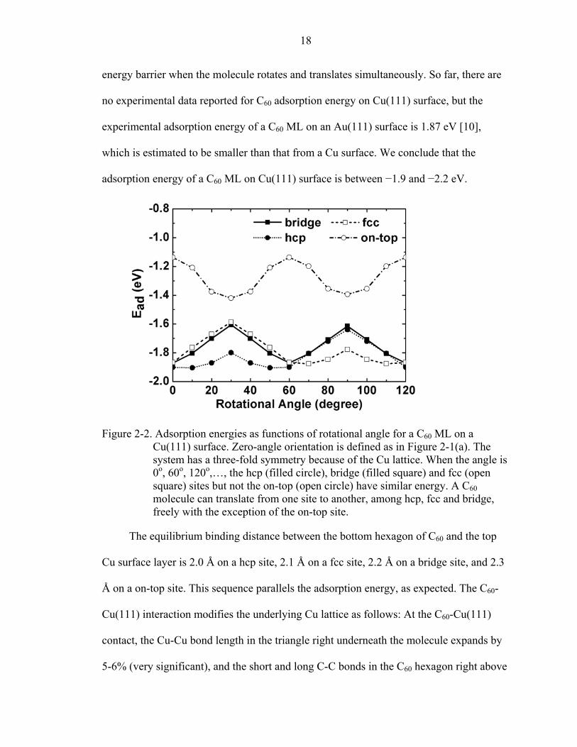
energy barrier when the molecule rotates and translates simultaneously. So far, there are
no experimental data reported for C60 adsorption energy on Cu(111) surface, but the
experimental adsorption energy of a C60 ML on an Au(111) surface is 1.87 eV [10],
which is estimated to be smaller than that from a Cu surface. We conclude that the
adsorption energy of a C60 ML on Cu(111) surface is between −1.9 and −2.2 eV.
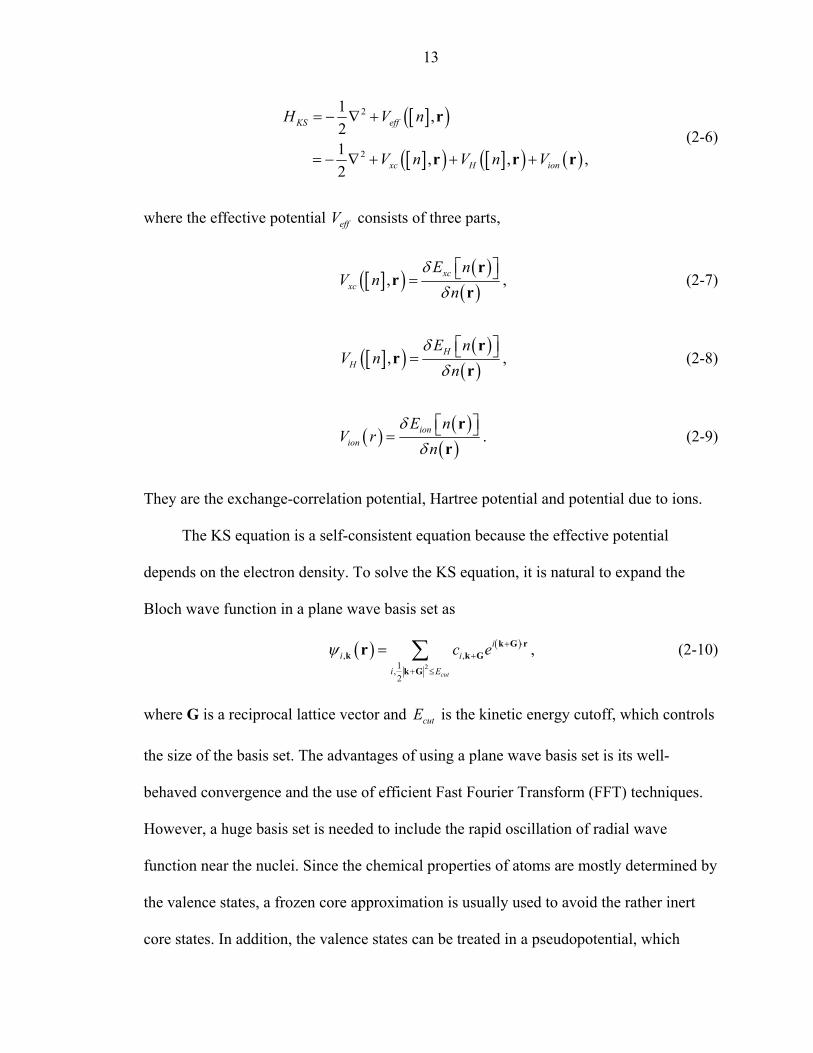
Figure 2-2. Adsorption energies as functions of rotational angle for a C60 ML on a Cu(111) surface. Zero-angle orientation is defined as in Figure 2-1(a). The system has a three-fold symmetry because of the Cu lattice. When the angle is 0o, 60o, 120o,…, the hcp (filled circle), bridge (filled square) and fcc (open square) sites but not the on-top (open circle) have similar energy. A C60 molecule can translate from one site to another, among hcp, fcc and bridge, freely with the exception of the on-top site.
The equilibrium binding distance between the bottom hexagon of C60 and the top
Cu surface layer is 2.0 Å on a hcp site, 2.1 Å on a fcc site, 2.2 Å on a bridge site, and 2.3
Å on a on-top site. This sequence parallels the adsorption energy, as expected. The C60-
Cu(111) interaction modifies the underlying Cu lattice as follows: At the C60-Cu(111)
contact, the Cu-Cu bond length in the triangle right underneath the molecule expands by
5-6% (very significant), and the short and long C-C bonds in the C60 hexagon right above

19
the Cu surface increase by 3% and 2% (not negligible); the Cu atoms beneath the
molecule lower their positions by 0.14 Å, and the Cu atoms surrounding the molecule rise
by 0.10 Å, with respect to the average atomic position in the surface layer. The
deformation and the perturbation from the molecule cause electrons in the surface to
undergo diffusive reflection when they encounter the interface, thus reducing the
conductance of a relatively thick metal film [17].
(a) (b) Figure 2-3. Total density of states and partial DOS projected on the C60 ML and the
Cu(111) surface. They are plotted in the full energy range and near the Fermi level in (a) and (b), respectively. The dashed vertical line represents the Fermi level.
2.3.1.2 Electronic Structures
To analyze electronic structure, the density of states and energy bands are projected
onto the C60 molecule and the Cu surface via the relationships
( ) ( ) ( ) ( )2
, ,i ii
g wµ µε δ ε ε φ ψ= −∑ ∑k k kk
r r (2-11)
and
( ) ( )2
, ,i ip wµ µφ ψ=∑ k kk
r r (2-12)
respectively. Here, µφ and ,iψ k are the atomic and Bloch wave functions, respectively; wk
is the weight of each k point, and the indices µ and (i,k) are labels for atomic orbitals

20
and Bloch states, respectively. The projection provides a useful tool for analyzing the
electronic band structure and the density of states.
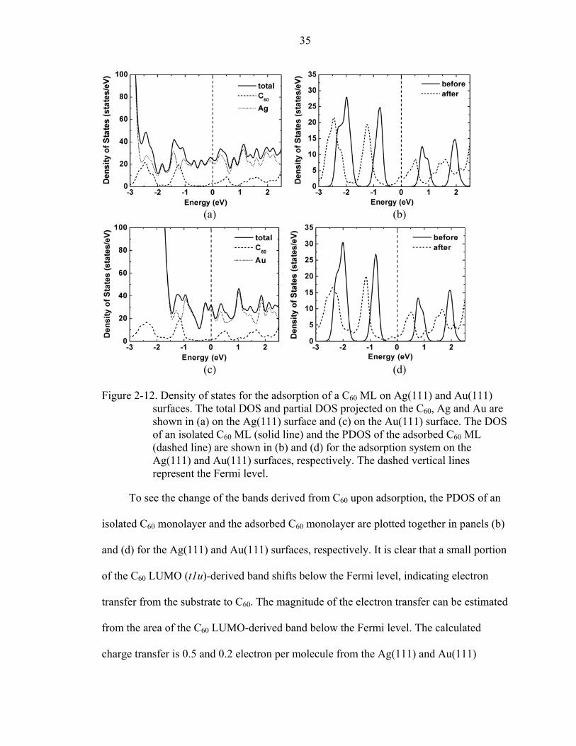
(a) (b)
(c) (d) Figure 2-4. Band structure for the adsorption of a C60 ML on a Cu(111) surface. (a) is the
first Brillouin zone of the two-dimensional space group of p3m1. The irreducible region is indicated by shadowing. (b) is the band structure of an isolated C60 ML near the Fermi level. (c) are the projection coefficients of the bands on the C60 (solid line) and the Cu surface (dotted line) near the Fermi level. (d) depicts two bands across the Fermi level that are likely to originate from the C60 LUMO(t1u)-derived bands. Their projections on the C60 ML are 3% and 13%, respectively.
The total density of states (DOS) and partial DOS projected on Cu and C60 of a C60
ML adsorbed on an hcp site with a hexagon parallel to the surface are shown in Figure 2-
3. The Fermi level is located above the range of the strong Cu d band as seen in Figure 2-
3(a). The sharp peaks below −8 eV indicate that the states in that low energy range are

21
modulated strongly by the features of the C60 ML. It can be seen in Figure 2-3(b) that the
DOS near the Fermi level is dominated by states from the Cu(111) surface.
Figure 2-5. DOS of an C60 ML before and after its adsorption on a Cu(111) surface. The solid and dashed line stand for before and after the adsorption, respectively.
The band structure of an isolated C60 ML is shown along the Γ-M-K-Γ directions in
Figure 2-4(b) together with the first surface Brillouin zone in Figure 2-4(a). It shows that
an isolated C60 ML is a narrow gap semiconductor, with a gap of 1.0 eV. The threefold
degeneracy in the LUMO (t1u) of a C60 molecule is lowered by the two-dimensional
symmetry. The LUMO turns into three bands closely grouped from 0.5 to 1.0 eV.
Projections of all bands near the Fermi level on C60 and Cu of the C60-Cu(111) system are
given in Figure 2-4(b). We found that projections on C60 are small fractions compared to
the metal surface. The band structure of the C60-Cu(111) system suggests a strong band
mixing, thus making it difficult to trace the origin of any given band. We identify two
energy bands that cross the Fermi energy in Figure 2-4(d), which are likely to be bands
from the t1u orbital of the isolated C60-ML. These bands have projections of only 3% and

22
13% on C60. It can be seen from these curves that the hybridization between molecular
and surface states is significant, indicating strong molecule-surface interactions.
The partial DOS projected on a C60 ML adsorbed on the Cu(111) surface (dashed
line) is compared to an isolated C60 ML (solid line) in Figure 2-5. Relative to the isolated
C60 ML, states near the Fermi energy of the adsorbed C60 ML have shifted to lower
energy as a result of molecule-surface interaction. The LUMO (t1u)-derived band is now
broadened and partially filled below the Fermi energy because of the surface-to-molecule
electronic charge transfer. The calculated DOS compares nicely with experimental results
from photoemission spectroscopy. This energy shift–charge transfer phenomenon is very
characteristic in molecule-surface interactions. It is a compromise between the two
systems: A strong bond between the molecule and the surface has formed at the cost of
weakening the interaction within both the C60 ML and within the metal surface.
Integration of the partially filled C60 LUMO(t1u)-derived band leads to a charge
transfer of 0.9 electrons per molecule from the copper surface to the adsorbed C60 ML.
To confirm the magnitude of charge transfer, we also implemented a modified Bader-like
approach [69] to analyze the electron density in real space. The bond critical plane is first
located by searching for the minimum electron density surface inside the C60-metal
interface region using
( ) 0z
ρ∂=
∂r
, (2-13)
where is the electron density and z is the direction normal to the Cu surface. Then
the electron density between the bond critical plane and the middle of the vacuum is
integrated and the result is assigned as the electrons associated with C
( )ρ r
60. A charge

23
transfer of 0.8 electrons per molecule is observed using this analysis from the surface to
the C60 molecule, which is in agreement with the analysis of the DOS.
(a) (b)
(c) (d) Figure 2-6. Partial DOS of different adsorption configurations for a C60 ML on a Cu(111)
surface. Partial DOS is projected on the bottom hexagon of C60 (upper panel in a-d) and on the first surface layer of Cu(111) surface (lower panel in a-d)

24
for different adsorption sites and orientations. Panel (a) is hcp (solid line) vs. fcc (dotted line); (b) hcp (solid line) vs. on-top (dotted line); (c) hcp (solid line) vs. hcp with a 90o rotation (dotted line); and (d) on-top (solid line) vs. on-top with a 30o rotation (dotted line).
Furthermore, to understand the energetic preference of different adsorption sites,
we analyze their DOS in Figure 2-6. The DOS is projected on the bottom hexagon of C60
and the top Cu surface layer in the upper and lower panel of Figure 2-6, respectively. It
can be seen in Figure 2-6(a) that the DOS of a fcc site differs very little from that of a hcp
site, which explains why they have very close adsorption energy. In Figure 2-6(b), the
DOS of an on-top site has a quite visible population shift, with respect to that of a hcp
site, from the bottom of the Cu d band around −3.5 eV to the top of the Cu d band around
−1.5 eV. It is well known [70] that the Cu bonding states, d , located at the bottom of
the d band and the anti-bonding states, , located at the top of the d band.
Consequently, an increased population in higher energy states means less bonding, while
an increased population in lower energy states indicate more bonding. This explains why
the on-top site has less binding energy than the hcp site, as reflected in the difference of
DOS. Similar features are also depicted for rotations of a C
xy
dx 2 − y 2
60 molecule on the hcp and the
on-top sites in Figure 2-6(c) and (d), respectively.
2.3.1.3 Electron Density Redistribution and Work Function Change
The electron density difference, ( )ρ∆ r , is obtained by subtracting the densities of
the clean substrate and the isolated C60 ML from the density of the adsorbate-substrate
system. This quantity gives insight into the redistribution of electrons upon the adsorption
of a C60 ML. In Figure 2-7 (a) and (b), the iso-surfaces of electron density difference are
plotted for binding distances of 2.0 Å and 2.8 Å for a C60 ML adsorbed on a hcp site with
a hexagon parallel to the surface. In both panels, the three-fold symmetry of the electron

25
density redistribution can be seen clearly. When C60 is at the equilibrium distance, 2.0 Å,
from the surface, the redistribution of electrons is quite complicated especially in the
interface region between the surface and the molecule as seen in Figure 2-7(a). To get a
better view, we plot the planar averaged electron density difference along the z direction,
, in the upper panels of Figure 2-8(a). ( )zρ∆
(a) (b) Figure 2-7. Iso-surfaces of electron density difference for a C60 ML on a Cu(111) surface.
Electron density decreases in darker (red) regions and increases in lighter regions (yellow): (a) depicts the equilibrium position and (b) corresponds to the C60 being lifted by 0.8 Å. The iso-surface values are ±1.0 and ±0.4 e/(10×bohr)3 in (a) and (b) respectively. The complexity of the distribution shown leads to a net charge transfer from the surface to the C60 ML and a dipole moment that is opposite to the direction of charge transfer.
Considering the charge transfer of 0.8 electrons per molecule from the surface to
C60, the simple picture of electrons depleting from the surface and accumulating on C60
can not be found in these figures. Instead, it is a surprise to see such complexity in the
electron density redistribution. The major electron accumulation is in the middle of the
interface region, which is closer to the bottom of C60 than the first Cu layer. This feature
of polarized covalent bonding results in a charge-transfer from the surface to the C60.
Some electron accumulation also happens around the top two Cu layers and inside the C60
cage. On the other hand, the major electron depletion is inside the interface region from

26
places near either the first Cu layer or the bottom hexagon of C60. There are also
significant contributions of electron depletion from regions below the first Cu layer and
inside the C60 cage. When the C60 is 0.8 Å away from the equilibrium distance, this
feature of electron depletion inside the C60 cage becomes relatively more pronounced as
seen in Figure 2-7(a) and the upper panel of Figure 2-8(b). This feature has important
effects on the surface dipole moment and the change of work function.
(a) (b) Figure 2-8. Planar averaged electron density differences (upper panel) and the change in
surface dipole moment (lower panel) for the adsorption of a C60 ML on a Cu(111) surface. Both are the functions of z, the direction perpendicular to the surface. The distance between the bottom hexagon of C60 and the first copper layer is 2.0 Å in (a) and 2.8 Å in (b). The solid vertical lines indicate the positions of the top two copper layers and the dashed vertical lines indicate the locations, in z direction, of the two parallel boundary hexagons in C60. The dotted horizontal line indicates the total change in the surface dipole moment.
The measured work functions (WF) of a clean Cu(111) surface and a C60 ML
covered Cu(111) surface from experiments are 4.94 and 4.86 eV [9], respectively. The
WF actually decreases by a tiny amount of 0.08 eV, although a significant charge transfer

27
from the substrate to C60 is observed in both experiments and our calculation. This result
is very puzzling with respect to the conventional interpretation of the relationship
between WF change and charge transfer. According to a commonly used analysis based
on simple estimation of a surface dipole moment, when electrons are transferred from
absorbed molecule to the surface the WF will decrease, while transfer the other way will
result in a WF increase.
To resolve this puzzling phenomenon and to investigate the issue thoroughly, we
employ two methods to calculate the work function change. One is to compute the
difference directly between the work function of the adsorption system and that of the
clean surface. The work function is obtained by subtracting the Fermi energy of the
system from the electrostatic potential in the middle of the vacuum. To calculate the work
function accurately, a symmetric slab with a layer of C60 adsorbed on both sides of the
slab or the surface dipole correction suggested by Neugebauer, et al. [71] have been used.
The results are given in Table V as 1W∆ and 2W∆ , respectively. To gain insight on the
origin of the change in the work function, we apply a method suggested by Michaelides,
et al. [72] to calculate the change in the surface dipole moment, µ∆ , induced by the
adsorption of C60. The quantity µ∆ is calculated by integrating the electron density
difference times the distance with respect to the top surface layer from the center of the
slab to the center of the vacuum,
( ) ( )2
0c
c
z a
zz z z dzµ
+∆ = − ∆∫ ρ (2-14)
In this equation, is the center of the slab, is the top surface layer and is the length
of the unit cell in the direction. The quantity
cz 0z a
z ( )zρ∆ is the planar averaged electron

28
density difference along the direction. The work function change, , is then
calculated according to the Helmholtz equation.
z ∆Φ
µ∆
0 Aµ
ε∆
∆Φ = (2-15)
where 0ε is the permittivity of vacuum and is the surface area of the unit cell. Both
and
A
∆Φ µ∆ are listed in Table 2-3.
Table 2-3. Work function change of a C60 ML adsorbed on a Cu(111) surface. and are calculated directly from the difference of the work functions with the
dipole correction and a double monolayer adsorption, respectively. is calculated from the change in the surface dipole moment,
1W∆
∆Φ2W∆
, induced by adsorption of C60.
Exp (eV) ∆W1 (eV) ∆W2 (eV) ∆Φ (eV) ∆µ (Debye) 2.0 Å −0.08a −0.10 −0.09 −0.09 −0.21 2.8 Å −0.37 −0.33 −0.32 −0.73 a. [9]
The calculated WF of a neutral C60-ML is 5.74 eV. The calculated WF of a pure
Cu(111) surface and C60 ML covered surface are 5.24 and 5.15 eV, respectively, which
are in good agreement with experiments (4.94 and 4.86 eV, respectively). The calculated
work function change is −0.09 eV, which agrees very well with the change of −0.08 eV
from experiments. The planar averaged charge density difference is depicted as a
function of in the upper panels of Figure 2-8 for the equilibrium distance, 2.0 Å and
the distance of 2.8 Å. In the lower panels, the integration of the surface dipole is shown
as a function of to capture its gradually changing behavior and the total value is shown
by a horizontal dotted line. For the equilibrium distance, the calculated
z
z
µ∆ is −0.21
Debye leading to a change of −0.09 eV in WF, ∆Φ , which is in excellent agreement
with both direct estimation and experiments. When the C60 is moved up from its
equilibrium position, by 0.8 Å in the z direction, the calculated charge transfer, change in

29
dipole moment, and work function are 0.2e-, −0.73 Debye and 4.91 eV (a 0.33 eV
decrease), respectively. The WF further decreases by −0.33 eV. The gradual change of
work function and charge transfer with respect to the binding distance are shown in
Figure 2-9. The results from the two direct estimation methods and the surface dipole
method match very well, especially over short distance ranges.
(a) (b) Figure 2-9. Work function change and electronic charge transfer as functions of the
distance between a C60 ML and a Cu(111) surface. The work function change and electronic charge transfer are shown in (a) and (b), respectively. The solid and dashed line shows the results from the dipole correction and the calculation using a double monolayer, respectively.
The change of surface dipole moment induced by molecule-surface interaction at
the interface is complicated in general; it cannot be estimated simply as a product of the
charge transferred and the distance between molecule and the surface. The electron
depletion region inside the C60 cage has great impact on the work function decrease as
seen in both Figure 2-7 and Figure 2-8. Its effect can only be taken into account with an
explicit integration in Eq.2-14. The change of work function is the result of a compromise
between the two systems: A strong bond formed between the C60 and the metal surface
occurs at the cost of weakening the interaction within both C60 and the metal surface,
since electrons must be shared in the interface region.

30
2.3.2 Adsorption of a C60 ML on Ag (111) and Au(111) Surfaces
2.3.2.1 Energetics and Adsorption Geometries
The ( 2 3 2 3× )R30o structure of a C60 monolayer adsorbed on Ag(111) and
Au(111) surfaces is shown in Figure 2-10(a). The calculated lattice constants of bulk Ag
and Au are 4.02 and 4.07 Å, respectively. The corresponding values of 9.85 and 9.97 Å
for the vector length of the ( 2 3 2 3× )R30o surface unit cell match closely with the
nearest neighbor distance in solid C60, which is 10.01 Å. Four possible adsorption sites
are considered, as shown in Figure 2-10(b), the on-top, bridge, fcc and hcp sites. To find
the lowest energy configuration on each adsorption site, we consider both a hexagon and
a pentagon of C60 in a plane parallel to the surface. Two parameters determine the lowest
energy configuration on each adsorption site with a certain face of C60 parallel to the
surface. One is the binding distance between the bottom of C60 and the top surface layer,
the other is the rotational angle of the C60 along the direction perpendicular to the surface.
The adsorption energies after ionic relaxation of the lowest energy configuration on each
site with a pentagon or a hexagon parallel to the surface are listed in Table 2-4. The
configuration of a hexagon of C60 parallel to the surface is more favorable energetically
than is a pentagon on all adsorption sites by an average of 0.3 eV for Ag(111) and 0.2 eV
for Au(111). With a hexagon of C60 parallel to both Ag(111) and Au(111) surfaces, the
most favorable site is the hcp, then the fcc and bridge sites. The on-top site is the least
favorable. The preference of the hcp over the fcc site is less than 0.1 eV. With a pentagon
of C60 parallel to both surfaces, the fcc site is slightly more favorable than the hcp site by
less than 0.01 eV. The rest of the ordering is the same as in the case of hexagon.

31
(a) (b) Figure 2-10. Surface geometry and adsorption sites for a C60 ML on Ag(111) and
Au(111) surfaces. (a) top view of C60 ML adsorbed on the Ag(111) and Au(111) surfaces (four unit cells are shown); (b) the ( 2 3 2 3× ) R30o
surface unit cell and the adsorption sites on the Ag(111) and Au(111) surfaces, 1, on-top; 2, fcc; 3, bridge; and 4, hcp site. Sites 2 and 4 are not equivalent due to differences in the lower surface layers (not shown).
Table 2-4. Adsorption energies of a C60 ML on Ag(111) and Au(111) surfaces on various sites. The energies listed are the lowest ones obtained after ionic relaxation. The energy is in unit of eV/molecule.
Configuration Hcp Fcc Bridge On-top Hexagon on Ag(111) -1.54 -1.50 -1.40 -1.27 Pentagon on Ag(111) -1.20 -1.20 -1.18 -0.89 Hexagon on Au(111) -1.27 -1.19 -1.13 -0.86 Pentagon on Au(111) -1.03 -1.04 -0.99 -0.60
The average binding distance between the bottom hexagon of C60 and the top
surface layer for different adsorption configurations is 2.4 Å for the Ag(111) surface and
2.5 Å for the Au(111) surface. For the same configurations, the adsorption energy of C60
on the Ag(111) surface is larger than that on the Au(111) surface by 0.3 eV. Thus the
binding of C60 monolayer with the Ag(111) surface is stronger than the binding with the
Au(111) surface as seen in both adsorption energies and binding distances. This finding is
in agreement with the experimental observation that the interaction between C60 and Au
is the weakest among the noble metals [10]. As seen in Table 2-4, a hexagon of C60 on an
hcp site is the most favored configuration on both surfaces, while a pentagon on an on-

32
top site is the least favored configuration. The difference in adsorption energy is about
0.7 eV for both surfaces. In STM experiments, Altman and Colton [13-15] proposed that
the adsorption configuration was a pentagon of C60 on an on-top site for both the Ag(111)
and Au(111) surfaces. However, Sakurai, et al. [16] proposed also from the results of
STM experiments, that the favored adsorption site should be the three-fold on-hollow site
on the Ag(111) surface, but they did not specify the orientation of the C60 molecule. Our
calculations support the model proposed by Sakurai, et al. For the Cu(111) surface, we
have shown earlier in this chapter that the adsorption configuration is a hexagon of C60 on
the three-fold on-hollow site. Based on the similarity of the electronic properties of the
noble metals, it is not unreasonable that C60 occupies the same adsorption site on Ag(111)
and Au(111) surfaces as on the Cu(111) surface.
(a) (b) Figure 2-11. Adsorption energies as functions of rotational angle of C60 ML on Ag(111)
and Au(111) surfaces. (a) on the Ag(111) surface, and (b) on the Au(111) surface. The zero angle orientation is defined in Figure 2-10(a) with a hexagon of C60 parallel to the surface on all sites.
To obtain the rotational barriers, we plot the adsorption energies as functions of the
rotational angle along the direction perpendicular to the surface on all sites with a
hexagon of C60 parallel to the surfaces in Figure 2-11. Since the binding distance on
various adsorption sites differs very little, less than 0.1 Å, with respect to rotational angle,

33
we keep the binding distance fixed during the rotation of C60 molecule. For each
rotational angle, the atomic positions are also fixed. The calculated rotational energy
barriers.
Table 2-5. The relaxed structure of a C60 ML adsorbed on Ag(111) and Au(111) surfaces with its lowest energy configuration. On both surfaces, the lowest energy configuration is a hexagon of C60 on the hcp site, as shown in Figure 2-10(a). The parameters C C
shortb −∆ and C Clongb −∆ are the relative change in the shorter and
longer bond of C60 with respect to a free molecule. The parameters M Mincb −∆
and M Mdecb −∆ are the maximum increase and decrease, respectively, in bond
length between two neighboring metal atoms in the top surface layer with respect to the bulk value. The parameter 11
M Md − describes the buckling, defined as the maximum vertical distance among the metal atoms in the top surface layer, and M Cd − is the average distance between the bottom hexagon of C60 and the top surface layer.
C Cshortb −∆ (%) C C
longb −∆ (%) M Mincb −∆ (%) M M
decb −∆ (%) 11M Md − (Å) M Cd − (Å)
Ag(111) 1.8 1.0 4.3 -1.2 0.02 2.29 Au(111) 1.8 1.4 7.3 -2.5 0.08 2.29
On both Ag(111) and Au(111) surfaces, the rotational barrier for the on-top site is
the highest, 0.5 eV for the Ag(111) surface and 0.3 eV for the Au(111) surface. The next
highest rotational barriers are on the fcc and hcp sites, which are 0.3 eV for the Ag(111)
surface and 0.2 eV for the Au(111) surface. Note that 30o and 90o rotations are not
equivalent due to the three-fold symmetry. The lowest rotational barriers are on the
bridge site, which are 0.2 eV for the Ag(111) surface and 0.1 eV for the Au(111) surface.
The rotational barriers on both surfaces are small enough that the C60 can rotate freely at
room temperature, which agrees with the experimental observations [13-15]. In general,
the rotational barriers on the Au(111) surface are lower than on the Ag(111) surface,
which is consistent with the weaker binding between C60 and the Au(111) surface than
the Ag(111) surface. This result is also in agreement with STM experiments, which show

34
that the on-site rotation of C60 on the Au(111) surface is faster than that on the Ag(111)
surface [13-15].
Several parameters of the relaxed structure in the lowest energy configuration on
both the Ag(111) and Au(111) surfaces are listed in Table 2-5. The lowest energy
configuration on both surfaces is a hexagon of C60 adsorbed on an hcp site, as shown in
Figure 2-10(a). On the Ag(111) surface, the bond lengths of the shorter and longer C-C
bonds in the bottom hexagon of the C60 increase by 1.8% and 1.0%, respectively, but the
bond length of the C-C bonds in the top hexagon of the C60 does not change. The
neighboring Ag-Ag bond lengths in the top surface layer increase by as much as 4.3% for
the atoms directly below the C60 and decrease by as much as 1.2% in other locations. The
relaxation of the Ag atoms in the top surface layer causes a very small buckling of 0.02
Å, which is defined as the maximum vertical distance among the Ag atoms. This value is
much less than the corresponding value of 0.08 Å on Au(111) surface. The average
vertical distance between the bottom of the C60 and the top surface layer is 2.29 Å. On the
Au(111) surface, the values of these parameters are somewhat larger than those on the
Ag(111) surface, which means that the Au(111) surface tends to reconstruct. However,
the interaction of C60 with the Ag(111) surface is still stronger than that on the Au(111)
surface as seen from the adsorption energies in Table 2-4.
2.3.2.2 Electronic Structure and Bonding Mechanism
The total density of states and partial density of states (PDOS) projected on C60 and
the substrate are shown in Figure 2-12 (a) and (c) for the Ag(111) and Au(111) surfaces,
respectively. The Ag 4d band is 3 eV below the Fermi level and the Au 5d band is 1.7 eV
below the Fermi level. The dominant features near the Fermi level are from the substrate.
35
(a) (b)
(c) (d) Figure 2-12. Density of states for the adsorption of a C60 ML on Ag(111) and Au(111)
surfaces. The total DOS and partial DOS projected on the C60, Ag and Au are shown in (a) on the Ag(111) surface and (c) on the Au(111) surface. The DOS of an isolated C60 ML (solid line) and the PDOS of the adsorbed C60 ML (dashed line) are shown in (b) and (d) for the adsorption system on the Ag(111) and Au(111) surfaces, respectively. The dashed vertical lines represent the Fermi level.
To see the change of the bands derived from C60 upon adsorption, the PDOS of an
isolated C60 monolayer and the adsorbed C60 monolayer are plotted together in panels (b)
and (d) for the Ag(111) and Au(111) surfaces, respectively. It is clear that a small portion
of the C60 LUMO (t1u)-derived band shifts below the Fermi level, indicating electron
transfer from the substrate to C60. The magnitude of the electron transfer can be estimated
from the area of the C60 LUMO-derived band below the Fermi level. The calculated
charge transfer is 0.5 and 0.2 electron per molecule from the Ag(111) and Au(111)

36
surfaces, respectively, to the C60 monolayer. These values are somewhat smaller than the
experimental estimate of 0.8 electrons per molecule on both surfaces [10, 22].
(a) (b)
(c) (d) Figure 2-13. Iso-surfaces of electron density difference for the adsorption of a C60 ML on
Ag(111) and Au(111) surfaces. Electron density decreases in darker (red) regions and increases in lighter (yellow) regions. The distance between the bottom hexagon of C60 and the first surface layer is 2.3 Å in (a) and 3.1 Å in (b) on the Ag(111) surface; and 2.4 Å in (c) and 3.2 Å in (d) on the Au(111) surface. The iso-surface value is ±1.0 e/(10×bohr)3 in (a) and (c), and ±0.4 e/(10×bohr)3 in (b) and (d).
Although there is some evidence from both theory and experiment for electronic
charge transfer from noble metal surfaces to C60, the nature of the bonding can not be
assigned as ionic without examination of the electron density difference; recall Section
2.3.1.3. The iso-surfaces of electron density difference are plotted for binding distances
of 2.3 Å and 3.1 Å for the Ag(111) surface in Figure 2-13 (a) and (b), and 2.4 Å and 3.2

37
Å for the Au(111) surface in Figure 2-13 (c) and (d). In all panels, the three-fold
symmetry of electron density redistribution can be seen clearly. As shown in panels (a)
and (c), the electron density redistribution is very similar for the adsorbed C60 monolayer
at the equilibrium binding distances on both the Ag(111) and Au(111) surfaces.
Three observations can be made from the data shown in Figure 2-13. First, the
change in the electron density is confined mostly to the top surface layer, the bottom half
of the C60, and the interface region. Close examination shows that the electron density in
the top half of the C60 changes very little, which agrees with the finding that no change in
the C-C bond length occurs after ionic relaxation. Second, there is significant electron
depletion around both the top surface layer and the bottom hexagon of the C60.
Specifically, the dumbbell shape lying in the direction perpendicular to the surface with a
small ring of electron accumulation near the top surface layer indicates the character of
noble metal dxz and dyz electrons. In addition to the electron density depletion region just
below the bottom hexagon of the C60, there are small regions inside the C60 cage and just
above the bottom hexagon, where the electron density also decreases. Third, although the
electron density increases in some regions just above the bottom hexagon of the C60, the
most significant electron accumulation occurs in the middle of the interface region, which
has a dumbbell shape parallel to the surface. When the C60 monolayer is pulled 0.8 Å
away from the equilibrium binding distances, the region with electron accumulation in
the middle of the interface can be seen more clearly in Figure 2-13 (b) and (d).
Evidently the electron density shared in the middle of the interface region derives
from both the Ag(111) and Au(111) surfaces and the C60 monolayer. As a result, the
bonding between them is best described as ionic-covalent with a small magnitude of

38
electronic charge transfer. The bond strength between the C60 monolayer and noble metal
surfaces decreases in the order Cu(111), Ag(111) and Au(111) according to both our
calculations and the experimental observations. The covalent bonding explains why a
hexagon is preferred to a pentagon when a C60 monolayer adsorbs on noble metal
surfaces. As is well known, for an isolated C60 molecule, the hexagon region has a higher
electron density than the pentagon region because the C60 HOMO is centered on the
bonds between two hexagons, and the C60 LUMO is centered on the bonds between a
hexagon and a pentagon. To form covalent bonds with noble metal surfaces, the hexagon
is more efficient than a pentagon because more electrons are available. If the bond were
ionic in nature, we would expect the most stable configuration to be a pentagon facing
toward the surface. Although similar, there are slight differences in the electron
redistribution in the C60-Ag(111) and C60-Au(111) systems. Specifically, the Au(111)
surface tends to spill out fewer electrons than the Ag(111) surface for sharing with the
C60. As a result, C60 on an Au(111) surface provides more electrons than it does on an
Ag(111) surface for covalent bonding. These different features have a large impact on the
different behavior of work function change on these two noble metal surfaces, which we
will discuss in detail in the following section.
To understand the energetic preferences of the various adsorption configurations,
the PDOS of a hexagon of C60 on an hcp site and two other configurations on the
Ag(111) and Au(111) surfaces are compared in Figure 2-14. The upper panels are the
PDOS projected on the bottom hexagon or pentagon of the C60 parallel to the surface.
The lower panels are the PDOS projected on the top surface layer.
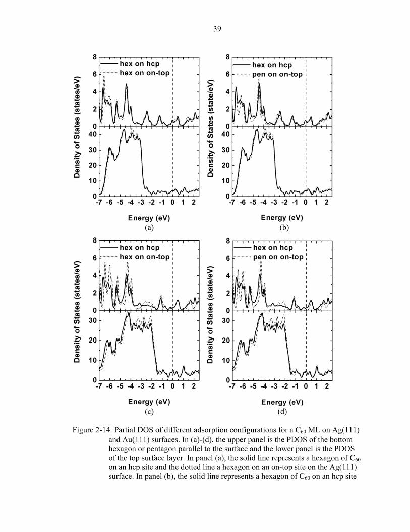
39
(a) (b)
(c) (d) Figure 2-14. Partial DOS of different adsorption configurations for a C60 ML on Ag(111)
and Au(111) surfaces. In (a)-(d), the upper panel is the PDOS of the bottom hexagon or pentagon parallel to the surface and the lower panel is the PDOS of the top surface layer. In panel (a), the solid line represents a hexagon of C60 on an hcp site and the dotted line a hexagon on an on-top site on the Ag(111) surface. In panel (b), the solid line represents a hexagon of C60 on an hcp site

40
and the dotted line a pentagon on an on-top site on the Ag(111) surface. In panel (c), the solid line represents a hexagon of C60 on an hcp site and the dotted line a hexagon on an on-top site on the Au(111) surface. In panel (d), the solid line represents a hexagon of C60 on an hcp site and the dotted line a pentagon on an on-top site on the Au(111) surface.
In Figure 2-14 (a), the PDOS of a hexagon of C60 on an hcp site is compared to that
of a hexagon on an on-top site on the Ag(111) surface. The figure shows that there are
more electrons from the on-top site than the hcp site populating the top of Ag d bands
around −3 eV, which are the anti-bonding states. This is the reason why the hcp site is
preferred to the on-top site. When comparing a pentagon of C60 on an on-top site with an
hcp site, this feature can also be seen in Figure 2-14 (b). In addition, the C60 LUMO-
derived bands of the hexagon shift further below the Fermi level than those of a
pentagon, which indicates more electronic charge transfer. The Bader-like analysis
confirms this interpretation by predicting 0.5 and 0.4 electrons transferred for these two
cases, respectively. The same argument can also be applied to the adsorption of C60 on
the Au(111) surface, as shown in Figure 2-14 (c) and (d). Comparing the PDOS in Figure
2-14 (b) and (d), we notice that the C60 HOMO−1 bands hybridize significantly with the
Au d bands, but stay unchanged on the Ag(111) surface. The reason for this behavior is
that the Au d bands are closer to the Fermi level than the Ag d bands. The Au d bands
align well with the C60 HOMO−1 bands.
2.3.2.3 Work Function Change
A puzzling phenomenon observed in C60-metal adsorption systems is the work
function change [10, 12]. Traditionally, work function change is associated closely with
the direction and the magnitude of electron transfer between the substrate and the
adsorbate. An increase in the work function indicates that electrons have been transferred
from the substrate to the adsorbate; a decrease in the work function indicates that

41
electrons have been transferred in the opposite direction. The argument can also be used
in an inverse sense. If electron transfer occurs from the substrate to the adsorbate, an
increase in the work function would be expected. For a C60 monolayer adsorbed on noble
metal surfaces, electron transfer from the surface to the C60 monolayer is observed in
both the experiments and our first-principles DFT calculations. As already discussed,
measurements of the work function in experiments have found that the work function
actually decreases for Cu(111) [9] and Au(111) [10] surfaces upon adsorption of a C60
monolayer.
Table 2-6. Work function change of a C60 ML adsorbed on Cu(111), Ag(111) and Au(111) surfaces. W∆ is calculated directly from the difference of the work functions. is calculated from the change in the surface dipole moment, ∆Φµ∆ , induced by adsorption of C60.
Exp (eV) W∆ (eV) ∆Φ (eV) µ∆ (Debye) Cu(111) -0.08a -0.09 -0.09 -0.21 Ag(111) +0.14 +0.11 +0.24 Au(111) -0.6b -0.58 -0.60 -1.37 a. [9] and b. [10]
We study this issue as in Section 2.3.1.3. The results are given in Table 2-6. The
work function change calculated from the direct difference is listed as . Once again,
the change in the surface dipole moment,
W∆
µ∆ , induced by the adsorption of C60 is
calculated by integrating the electron density difference times the distance with respect to
the top surface layer from the center of the slab to the center of the vacuum as in Eq. 2-
14. The work function change, ∆Φ , is then calculated according to the Helmholtz
equation in Eq. 2-15. Both and ∆Φ µ∆ are listed in Table 2-6. For comparison, we also
list in Table 2-6 the results for a C60 monolayer adsorbed on a Cu(111) surface in the
(4×4) surface unit cell [73] from Table 2-3.

42
(a) (b)
(c) (d) Figure 2-15. Planar averaged electron density differences (upper panel) and the change in
surface dipole moment (lower panel) for the adsorption of a C60 ML on Ag(111) and Au(111) surfaces. They are the functions of z, the direction perpendicular to the surface. The distance between the bottom hexagon of the C60 and the first Ag(111) surface layer is 2.3 Å in (a) and 3.1 Å in (b). The distance is 2.4 Å in (c) and 3.2 Å in (d) for C60 adsorbed on the Au(111) surface. The solid vertical lines indicate the positions of the top two surface layers and the dashed vertical lines indicate the positions of the two parallel boundary hexagons in C60. The dotted horizontal line indicates the total change in the surface dipole moment.

43
As seen in Table 2-6, the work function change for the Au(111) surface is −0.58 eV
via the direct calculation and −0.60 eV via the surface dipole calculation, which agrees
very well with the experimental value of −0.6 eV [10]. The corresponding change in the
surface dipole is −1.37 Debye. For the Ag(111) surface, we find the work function
change is +0.14 eV and +0.11 eV using the two methods, respectively. The change in the
surface dipole in this case is +0.24 Debye. There are no experimental data on the work
function change for the C60-Ag(111) system. However, experimentally the work function
increases by 0.4 eV for C60 adsorbed on an Ag(110) surface [11], which supports our
results.
Despite the opposite change of the work function on the Ag(111) and Au(111)
surfaces upon C60 adsorption, calculations of the change in the surface dipole moment
reproduce the work function change very well. This result suggests that the origin of the
work function change is indeed the dipole formation around the interface. The simple
picture of electronic charge transfer of an ionic nature from the substrate to the adsorbate
fails to describe the entire picture of the complicated surface dipole formation.
A full understanding of the different behavior of the work function change on
Ag(111) and Au(111) surfaces requires close examination of the electron density
differences. To elucidate more clearly, the planar averaged electron density differences
along the z direction are shown in the upper panels of Figure 2-15 (a) and (c) at the
equilibrium binding distances. The top surface layer is at zero distance, as indicated by a
solid vertical line. The interface region is between the solid vertical line at zero and the
nearby dashed vertical line at 2.0 Å. As discussed in the previous section, the common
feature of both figures is the indication of covalent bonding rather than ionic bonding.

44
Electron density spills out from the top metal surface layer, which increases the surface
dipole. At the same time, electron density from C60 also spills out from the cage toward
the interface region, which decreases the surface dipole. For approximately the same
amount of electron accumulation in the middle of the interface region, the electron
depletion from the Ag(111) surface is larger than that from the Au(111) surface. At the
same time, electron depletion around the C60 is smaller on the Ag(111) surface than on
the Au(111) surface. These differences in the multiple dipole formations result in the
increase of the surface dipole for C60 adsorbed on the Ag(111) surface and decrease of
the surface dipole for C60 adsorbed on the Au(111) surface, as shown in the lower panels
in Figure 2-15 (a) and (c). When the C60 monolayer is pulled 0.8 Å away from the
equilibrium distance, there is still significant electron depletion from C60 on the Ag(111)
surface as seen in Figure 2-15 (b). On the Au(111) surface, at 0.8 Å away from the
equilibrium distance, as seen in Figure 2-15 (d), the electron accumulation in the middle
of the interface region comes even more from the C60 than from the metal surface. These
features can also be seen in the three dimensional graphs in Figure 2-13 (b) and (d).
The distance dependence of the work function change on the Ag(111) and Au(111)
surfaces is shown in Figure 2-16 (a) and (c). On both surfaces, the work function
decreases as the distance increases. To explain this observation, we plot the electronic
charge transfer as a function of distance in Figure 2-16 (b) and (d). The charge transfer
decreases as the distance increases. Less charge transfer means less electron density spills
out from the surface and the bonding is less ionic in character, becoming more covalent
as the distance increases. These observations are consistent with the electron density
difference analysis in Figure 2-13 and 2-15. So relatively more electrons in the middle of
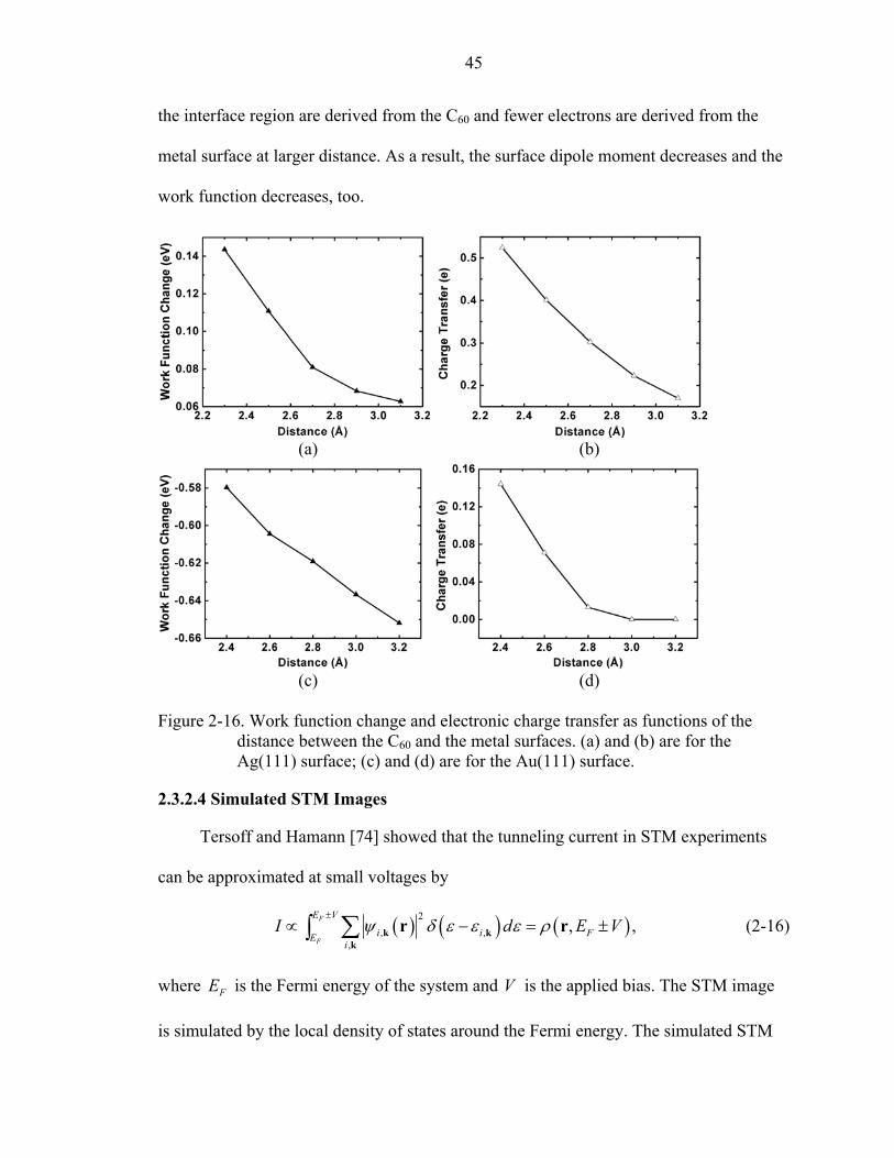
45
the interface region are derived from the C60 and fewer electrons are derived from the
metal surface at larger distance. As a result, the surface dipole moment decreases and the
work function decreases, too.
(a) (b)
(c) (d) Figure 2-16. Work function change and electronic charge transfer as functions of the
distance between the C60 and the metal surfaces. (a) and (b) are for the Ag(111) surface; (c) and (d) are for the Au(111) surface.
2.3.2.4 Simulated STM Images
Tersoff and Hamann [74] showed that the tunneling current in STM experiments
can be approximated at small voltages by
( ) ( ) (2, ,
,,F
F
E V
i i FEi
) ,I d Eψ δ ε ε ε ρ±
∝ − =∑∫ k kk
r r V± (2-16)
where is the Fermi energy of the system and V is the applied bias. The STM image
is simulated by the local density of states around the Fermi energy. The simulated STM
FE

46
images of the most favorable adsorption configuration are shown in Figure 2-17 for a C60
monolayer adsorbed on the Ag(111) surface ((a) and (b)) and the Au(111) surface ((c)
and (d)). A bias of −2.0 V is used in panels (a) and (c), and +2.0 V is used in (b) and (d).
The STM image is simulated by the local density of states at the position of 1.5 Å above
the top of C60 monolayer.
(a) (b)
(c) (d) Figure 2-17. Simulated STM images for a C60 ML adsorbed on Ag(111) and Au(111)
surfaces. Panels (a) and (b) are for the Ag(111) surface with a bias of -2.0 and +2.0 V, respectively. Panels (c) and (d) are for the Au(111) surface with a bias of -2.0 and +2.0 V, respectively. On both surfaces, the tip is 1.5 Å away from the top of the C60.
The images on the different surfaces are almost the same. The negative bias
produces a ring-like shape and the positive bias produces a three-leaf shape. These
images are in good agreement with the STM images simulated by Maruyama, et al. [47]
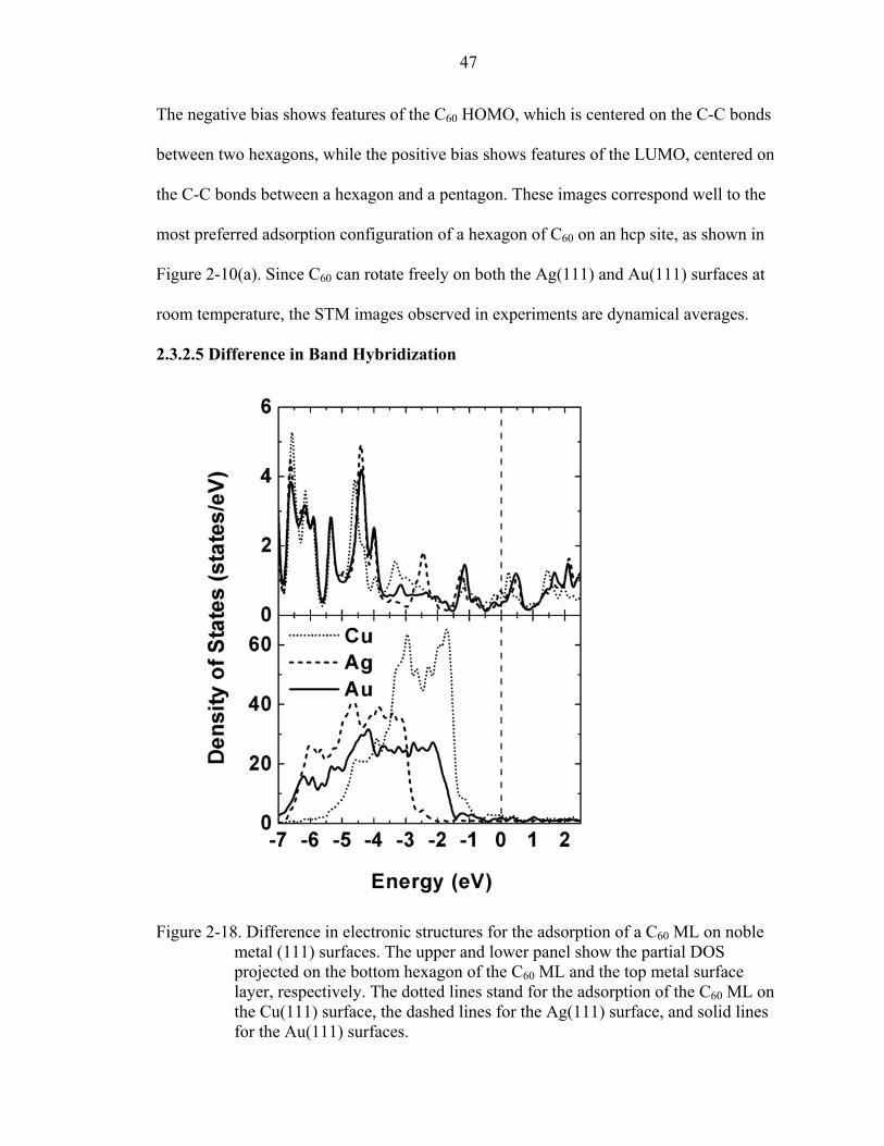
47
The negative bias shows features of the C60 HOMO, which is centered on the C-C bonds
between two hexagons, while the positive bias shows features of the LUMO, centered on
the C-C bonds between a hexagon and a pentagon. These images correspond well to the
most preferred adsorption configuration of a hexagon of C60 on an hcp site, as shown in
Figure 2-10(a). Since C60 can rotate freely on both the Ag(111) and Au(111) surfaces at
room temperature, the STM images observed in experiments are dynamical averages.
2.3.2.5 Difference in Band Hybridization
Figure 2-18. Difference in electronic structures for the adsorption of a C60 ML on noble metal (111) surfaces. The upper and lower panel show the partial DOS projected on the bottom hexagon of the C60 ML and the top metal surface layer, respectively. The dotted lines stand for the adsorption of the C60 ML on the Cu(111) surface, the dashed lines for the Ag(111) surface, and solid lines for the Au(111) surfaces.

48
The difference in electronic structures for the adsorption of a C60 ML on a noble
metal (111) surface is shown in Figure 2-18 by the partial density of states projected on
the bottom hexagon of C60 and on the top metal surface layer. The Cu 3d band is 1 eV
below the Fermi level, while the Ag 4d band is 3 eV below the Fermi level. The
consequence is that the Cu 3d band hybridizes much more with the C60 HOMO−1
derived band because of the better alignment. As for the case of Au 5d band, because of
relativistic effects [75], it is broadened and pushed toward the Fermi level. The resulting
Au 5d band is only 1.7 eV below the Fermi level, which also has stronger hybridization
with the C60 HOMO−1 derived band than Ag 4d band. This explains why the C60 ML has
the smallest electron depletion on Ag(111) surface among the three noble metals. Thus,
unlike Cu(111) and Au(111) surfaces, the Ag(111) surface has a decrease in work
function upon the adsorption of the C60 ML.
2.3.3 Adsorption of C60 ML on Al(111) and Other Surfaces
The adsorption of C60 on various surfaces other than noble metal (111) surfaces has
also been studied [8, 12]. From experiments, it has been found that C60 is weakly bonded
to graphite and silica surfaces. The interaction is mostly of van der Waals type. Very
strong covalent bonding has been found between C60 and Si, Ge and transition metal
surfaces. The strength of the bonding between C60 and noble metal surfaces is in the
middle of these two categories. From our first-principles DFT calculations, the bonding
between a C60 ML and noble metal (111) surface has features of both covalent and ionic
character. Another metal surface that binds C60 at similar strength as the noble metal
surfaces is Al. Al is also a fcc metal with the lattice constant of 3.76 Å, which is about
6% smaller than that of Ag and Au. It has been found from both experiments [12] and

49
first-principles calculation [49] that the ( 2 3 ) surface structure of a C2 3× 60 ML
adsorbed on Al(111) surface is only a metastable phase. The underlying Al atoms tend to
reconstruct and form a more stable (6×6) surface structure with one out three C60 lifted.
The bonding between C60 and Al(111) surface has been claimed to be predominantly
covalent.
(a) (b)
Figure 2-19. Density of states for the adsorption of a C60 ML on a Al(111) surface. In (a), the total DOS, the partial DOS projected on the C60 ML and the Al(111) surface are shown. The DOS of an isolated C60 ML (solid line) and the PDOS of the adsorbed C60 ML (dashed line) are shown in (b). The dashed vertical lines represent the Fermi level.
As a comparative study, we investigate the bonding of a C60 ML with Al(111)
surface in the same ( 2 3 2 3× ) surface structure as the Ag(111) and Au(111) surfaces.
For this metastable structure, we found that the most favored adsorption site is the hcp
site with a hexagon of C60 parallel to the surface. The binding distance between C60 and
the Al(111) surface is 2.5 Å, and the adsorption energy is −1.5 eV, which are close to the
results for the noble metal (111) surfaces. In Figure 2-19 (a) the total DOS and partial
DOS projected on C60 and Al are shown. The dominant feature around the Fermi level is
from the Al s and p electrons. As seen in Figure 2-19 (b), the HOMO-1 and LUMO

50
derived bands of an isolated C60 ML are broadened and slightly split as compared to
those in Figure 2-12 (b) and (d). This change is caused by the stress induced by the
smaller lattice constant of Al compared to Ag and Au. After its adsorption on Al(111)
surface, the C60 derived bands shift toward lower energy and part of the LUMO (t1u)-
derived band shifts below the Fermi level in a similar pattern to those for a C60 ML
adsorbed on noble metal (111) surfaces. This shows there is also a significant electronic
charge transfer from the Al(111) surface to the adsorbed C60 ML.
(a) (b) Figure 2-20. Electron density difference and change in surface dipole moment for a C60
ML on a Al(111)surface. The binding distance is 2.5 Å. In (a), the Iso-surfaces of electron density difference are shown at the value of ±1.0 e/(10×bohr)3. Electron density decreases in darker (red) regions and increases in lighter (yellow) regions. The planar averaged electron density difference and the change in surface dipole moment are shown in the upper and lower panel of (b), respectively. The solid vertical lines indicate the positions of the top two surface layers and the dashed vertical lines indicate the positions of the two parallel boundary hexagons in C60. The dotted horizontal line indicates the total change in the surface dipole moment

51
In Figure 2-20(a), the electron density difference is shown for the equilibrium
binding distance of 2.5 Å on the hcp site. The planar averaged electron density difference
and the integration of the change in surface dipole are also shown in Figure 2-20(b).
Compared with those for the noble metal (111) surfaces, the electron depletion from the
bottom hexagon of C60 is very small, much less than that from the Al (111) surface, and
the electron accumulation region is even closer to the bottom hexagon of C60 than for any
noble metal surface. This combination indicates a large electronic charge transfer. The
magnitude of the charge transfer is evaluated to be 1.0 electrons per molecule, which is
larger than the value of 0.8 for Cu(111) surface. The corresponding surface dipole change
is 2.10 Debye, which corresponds to an increase of 0.90 eV in work function.
Consequently, we think the interaction between C60 and Al(111) surface has more ionic
feature than noble metal (111) surfaces.
The surface reconstruction has also been found for a C60 ML adsorbing on open
surfaces of noble and transition metals, such as (110) and (100) surfaces. Generally, a
much larger surface unit cell is needed to include surface reconstruction. The study of
such adsorption systems poses a great challenge for large scale first-principles DFT
calculation. With more efficient algorithms, faster computer hardware, and new
developments in multiscale modeling, such as the embedding atom-jellium model
presented in Chapter 4, these issues of C60 induced surface reconstruction will be
addressed in the near future.
2.3.4 Adsorption of SWCNT on Au(111) Surface
Another fullerene that also attracts intensive research is the single wall carbon
nanotube (SWCNT). In experiments [76], it has been used to construct a single electron
transistor and thus is regarded as a promising candidate for future nano-electronics. In

52
these experiments, a SWCNT is always used with Au electrodes. The study of the
adsorption of SWCNTs on an Au surface therefore is of basic interest. It has been found
from first-principles calculations that the outer wall of a SWCNT interacts weakly with
Au surface [77, 78]. In this section, we carry out first-principles DFT calculation to study
the adsorption of a metallic (5,5) and a semiconductor (8,0) SWCNT on Au(111) surface.
SWCNTs come in two flavors, metallic and semiconducting, depending on the
chirality (n,m) of the underlying graphite sheet. When the Brillouin zone boundary of a
SWCNT unit cell crosses with the apex of the underlying Brillouin zone of graphite, the
SWCNT is metallic, otherwise, semiconducting. This is summarized in the following
formula for an arbitrary (n,m) SWCNT,
0,mod
,3metallicn m
nonzero semiconducting− =
(2-17)
There are exceptions for SWCNT with very small diameters. For example, large
curvature makes the (5,0) SWCNT metallic [79]. There are two groups of SWCNT with
the shortest repeating unit cells: the armchair (n,n) with the lattice constant of ga , and the
zig-zag (n,0) with the lattice constant of 3 ga , where ga is the lattice constant of the
underlying graphite.
Once again, we use LDA with ultrasoft pseudopotentials as implemented in VASP
to do the calculation. The lattice constant of fcc Au is 4.07 Å. The structure of free-
standing SWCNT is first calculated. The starting C-C bond length is 1.42 Å for both
armchair and zig-zag SWCNT. After relaxation, the bond length in the axial direction is
increased to 1.44 Å and the bond length is decreased to 1.40 Å in other directions. To
accommodate several unit cells of SWCNT on an Au(111) lattice, the in-plane lattice

53
constant of Au must be shrunk a little. For a (5,5) SWCNT, we construct the (4× 3 )
surface unit cell to include three SWCNT cells by shrinking the in-plane Au lattice
constant by 2%. For a (8,0) SWCNT, we construct the (2 3 ×3) surface unit cell to
include three SWCNT cells by shrinking the in-plane Au lattice constant by 3%. The
dimensions of the surface unit cells are large enough that the interaction between two
neighboring SWCNTs is negligible.
To find the lowest energy configuration for a SWCNT adsorbed on a Au(111)
surface, we first rotate the tube along its axis to search for the optimal orientation. Then
we search for the adsorption site which gives the lowest energy with this orientation. A
metallic (5,5) SWCNT prefers to adsorb with a hexagon, rather than a zig-zag C-C bond
along the axial direction, facing down to the surface. The most favorable adsorption site
for the hexagon is the site halfway between a hcp and bridge site. The binding distance is
2.9 Å and adsorption energy is −0.13 eV/Å. A semiconducting (8,0) SWCNT prefers to
adsorb with both a hexagon and an axial C-C bond facing down to the surface. The
lowest energy configuration corresponds to one of the axial C-C bonds centered on a
bridge site. The binding distance is 2.9 Å and the adsorption energy is −0.13 eV/Å, which
are the same as for the (5,5) SWNT. For both tubes, the energy preference over any other
adsorption configuration is very small. So a SWCNT can easily roll and translate on a
Au(111) surface. The strength of the interaction between a SWCNT and a Au(111)
surface is much weaker than that of a C60 ML, as indicated in both the binding distance
and adsorption energies.
The density of states for the adsorption of a (5,5) SWCNT on a Au(111) surface is
shown in Figure 2-21. The partial DOS projected on the tube remains almost the same,

54
before and after its adsorption on the Au surface. In contrast to the large shift of the C60
derived bands toward lower energy when a C60 ML adsorbs on a Au(111) surface, the
(5,5) SWCNT derived bands shift slightly toward higher energy. This indicates that the
electronic charge transfer is from the tube to the Au surface. This is reasonable since the
(5,5) SWCNT has the work function of 4.61 eV, which is much lower than 5.4 eV of the
Au(111) surface as indicated from our DFT-LDA calculations.
(a) (b)
Figure 2-21. Density of states for the adsorption of a (5,5) SWCNT on a Au(111) surface. In (a), the total DOS, the partial DOS projected on the SWCNT and the Au(111) surface are shown. The DOS of an isolated SWCNT (solid line) and the PDOS of the adsorbed SWCNT (dashed line) are shown in (b). The dashed vertical lines represent the Fermi level.
The charge transfer from a (5,5) SWCNT to a Au(111) surface is clearly shown by
the electron density difference in Figure 2-22. Substantially more electrons are depleted
from the tube than from the Au surface to form an electron accumulation region inside
the interface. The amount of charge transfer is 0.09 electrons per surface unit cell. The
induced change in the surface dipole is −1.30 Debye, as see in Figure 2-22 (b), which
corresponds to a decrease in the work function of the combined system with respect to
the Au(111) surface by 0.90 eV.

55
(a) (b) Figure 2-22. Electron density difference and change in surface dipole moment for a (5,5)
SWCNT on a Au(111)surface. The binding distance is 2.9 Å. In (a), the Iso-surfaces of electron density difference are shown at the value of ±1.0 e/(10×bohr)3. Electron density decreases in darker (red) regions and increases in lighter (yellow) regions. The planar averaged electron density difference and the change in surface dipole moment are shown in the upper and lower panel of (b), respectively. The solid vertical lines indicate the positions of the top two surface layers and the dashed vertical lines indicate the boundaries of the SWCNT. The dotted horizontal line indicates the total change in the surface dipole moment.
The density of states for the adsorption of a (8,0) SWCNT on a Au(111) surface is
shown in Figure 2-23. Unlike a (5,5) SWCNT, the bands derived from the (8,0) SWCNT
do not shift in a uniform way when it adsorbs on the Au(111) surface. The HOMO−1
derived band shifts toward higher energy, while the HOMO, LUMO and LUMO+1
derived bands shift toward lower energy with considerable broadening.

56
(a) (b)
Figure 2-23. Density of states for the adsorption of a (8,0) SWCNT on a Au(111) surface. In (a), the total DOS, the partial DOS projected on the SWCNT and the Au(111) surface are shown. The DOS of an isolated SWCNT (solid line) and the PDOS of the adsorbed SWCNT (dashed line) are shown in (b). The dashed vertical lines represent the Fermi level.
(a) (b) Figure 2-24. Electron density difference and change in surface dipole moment for a (8,0)
SWCNT on a Au(111)surface. The binding distance is 2.9 Å. In (a), the Iso-surfaces of electron density difference are shown at the value of ±1.0 e/(10×bohr)3. Electron density decreases in darker (red) regions and increases in lighter (yellow) regions. The planar averaged electron density difference

57
and the change in surface dipole moment are shown in the upper and lower panel of (b), respectively. The solid vertical lines indicate the positions of the top two surface layers and the dashed vertical lines indicate the boundaries of the SWCNT. The dotted horizontal line indicates the total change in the surface dipole moment
The electron density difference shown in Figure 2-24 indicates an electronic charge
transfer from the tube to the surface. Similar to the case of a (5,5) SWCNT, there are
many more electrons depleted from the tube than the Au surface. The amount of charge
transfer is 0.14 electrons per surface unit cell. The induced surface dipole is −2.14 Debye,
which corresponds to 0.90 eV decrease in the work function after division by the surface
area of the unit cell. The planar averaged electron density difference for the (8,0)
SWCNT adsorbed on the Au(111) surface has almost the same features as that for a C60
ML adsorbed on the Au(111) surface shown in Figure 2-15 (d) at the binding distance of
3.2 Å.
2.4 Conclusion
In summary, we have presented a detailed microscopic picture of the interaction
between a C60 ML and noble metal (111) surfaces. Large-scale first-principles DFT
calculations have provided complete microscopic picture of the interaction between a C60
ML and noble metal (111) surfaces. We find that the most energetically preferred
adsorption configuration on all noble metal (111) surfaces corresponds to a hexagon of
C60 aligned parallel to the surface and centered on an hcp site. The strength of the
interaction between the C60 ML and noble metal (111) surfaces decreases in the order of
Cu, Ag and Au. Analysis of the electron density difference and density of states indicates
that the interaction between C60 and the noble metal surfaces has a strong covalent
character besides the ionic character (a small amount of electronic charge transfer from
the surfaces to C60). This picture is in contrast with the common notion, developed from

58
experiments, that the interaction between C60 and noble metal surfaces is mostly ionic.
The puzzling observation of the work function change on noble metal surfaces can only
be explained by including this covalent feature and close examination of the surface
dipole formation in the interface region.
For comparison, we have studied the adsorption of a C60 ML on a Al(111) surface
in the ( 2 3 ) structure. The interaction between a C2 3× 60 ML and the Al(111) surface
shows more ionic character than noble metal (111) surfaces with larger electronic charge
transfer from the surface to the C60.
In addition, we have also studied the adsorption of SWCNTs on a Au(111) surface.
The strength of the interaction between the Au(111) surface and SWCNTs is much
weaker than that of a C60 ML. We find a very small electronic charge transfer from the
SWCNTs to the Au(111) surface and the SWCNTs become p-doped.

CHAPTER 3 MOLECULAR DYNAMICS SIMULATION OF POTENTIAL SPUTTERING ON LIF
SURFACE BY SLOW HIGHLY CHARGED IONS
3.1 Introduction
In recent years, with developments in ion-source technology such as the electron
beam ion trap [80-85] and electron cyclotron resonance [86], highly charged ion (HCI)
beams with charge states q greater than 44 have become available. In these experiments,
electron beams with a given energy and density collide with the target ions and strip off
their electrons. The resulting HCIs are then magnetically mass-to-charge separated into
an ultrahigh vacuum chamber. The HCI beam is then decelerated before it bombards the
target surface. The kinetic energy of the HCI can be as low as 5 q× eV [87]. Because of
the potential application of these energetic particles in nanoscale science, the interaction
of HCIs with solid surfaces has become one of the most active areas in the field of
particle-solid interactions. A HCI possesses a large amount of potential energy, which in
slow (hyperthermal) collision with a solid surface can greatly exceed its kinetic energy
and therefore dominate the ion-surface interaction. The subject includes a rich variety of
physical phenomena of both fundamental and applicational importance.
Investigations that focus on the neutralization dynamics of HCI projectiles have
revealed the following features [88-93]: When a HCI projectile approaches a surface, the
potential energy barrier between the surface and the available empty Rydberg states of
the HCI projectile decreases. Below a certain approach distance, electrons can be
captured via resonant neutralization (RN) and a so-called hollow atom can form rapidly.
59
60
The emission of secondary electrons and the formation of dynamical screening charges
give rise to strong image interactions between the HCI projectile and the surface. When
the HCI projectile enters the surface, further RN and Auger neutralization can take place
and fill the inner shell vacancies of the HCI projectile and finally neutralize it. Fast Auger
electrons and X-rays can be emitted in this process. Despite the complex nature of the
problem, a classical over-barrier model (COB) [88, 89] has successfully explained the
image energy gain in the reflected HCI beam. In the experiments with a HCI beam at
grazing incidence on a metal or insulator surface, the 3 2q dependence of the image
energy gain can be derived by the simple COB model [89, 92, 93]. Detailed simulations
based on the stair-wise COB model [94] and the dynamical COB model [95] have also
been performed to reproduce the experimental results.
The high potential energy of a HCI projectile at a surface can be released either via
emission of electrons and photons (X-rays), or via structure distortion and sputtering of
the target surface ions, atoms, or molecules. The surface modification caused by the
incident ions varies according to the material characteristics of the target surfaces.
Bombardment of metallic surfaces such as Au [96-99], Cu [100] is exclusively dominated
by kinetic energy transfer from the HCI projectile to target surface particles. In this case,
part of the potential energy of the HCI is transformed to kinetic energy due to the
interaction between the HCI and the surface. For semiconductor and insulator surfaces
such as Si [99, 101-104], GaAs [101, 102, 105], LiF [87, 101, 102, 106-115], SiO2 [99,
101, 102, 108, 116], and metal oxides [101, 102, 114, 117, 118], the sputtering patterns of
target surface particles are found to be highly sensitive to the charge states of the
projectile ions. This process is known as potential sputtering or electronic sputtering as

61
opposed to the conventional sputtering caused by kinetic energy transfer [87, 108]. In
contrast to metals, the valence electrons in insulators are localized. An insulator surface
has a considerably larger effective work function than a metal because of its large band
gap. Consequently, a smaller secondary electron yield is observed in the experiments [87,
101, 102]. The localized electronic excitation and electron-hole pairs in the valence bands
can survive long enough to convert potential energy into kinetic energy of sputtered
target surface particles.
Among the above-mentioned systems, LiF surfaces display unique features when
interacting with a HCI. Solid LiF is well known for its strong electron-phonon coupling,
which is the cause of electron and photon stimulated desorption [119-122]. Experimental
studies of collisions between slow HCIs such as Arq+ ( q =4, 8, 9, 11, and 14) or Xeq+
( q 14, 19, and 27) and LiF surfaces have been reported in recent years [87, 101, 106-
115]. The measured sputtering yields increase drastically with increasing incident HCI
charge states (i.e., higher electrostatic potential energy). To capture the characteristic
feature of strong electron-phonon coupling as mentioned above, a defect-mediated
sputtering model (DMS) [87, 101, 102, 108, 111, 123, 124] has been proposed as the
mechanism accounting for the observed potential sputtering of LiF surfaces by slow
HCIs. According to this model, the electronic excitation in the F(2p) valence band is
trapped into a highly excited electronic defect, namely, self-trapped excitons (STE).
Above room temperature the STE can decay immediately into a pair of H and F-color
centers. A H-center is a F molecular ion at an anion lattice site. A F-center is an electron
at the next or the second next anion lattice site relative to the Li
=
2−
+ cation. These H-and F-
color centers are highly mobile at room temperature and decay by emitting F0 atoms and
62
neutralizing Li+ cations, respectively, when reaching the surface. The desorption or
sputtering of the atoms is the result of a series of bond-breaking processes.
In order to understand the underlying physical mechanisms for various surface
modification, other models have also been proposed. For Si, the Coulomb explosion
model [125] as well as the bond-breaking model [126-128] have been used to explain the
dynamical process. Molecular dynamics (MD) simulations have been reported to
demonstrate the dynamical consequences of the proposed mechanisms [129-132]. While
Coulomb explosion and bond-breaking model are successful in many systems, they are
unable to describe the specific electronic excitations in LiF.
Inspired by the experimental findings, we formulate a model for MD simulations to
study HCI-LiF systems. The model involves high-level quantum chemistry calculations
as well as MD simulations under a variety of initial conditions. We aim to understand
surface modification processes, the dynamics of surface particles (both atoms and ions),
and the correlation of initial conditions with final sputtering outcome. The chapter is
organized in the following manner: Section 3.2 discusses the modeling and simulation,
section 3.3 presents results and discussion, and section 3.4 contains the conclusions.
3.2 Modeling and Simulation
The difficulties of applying MD to HCI-surface interactions come from the fact that
multiple electronic excitations and nuclear motion are entangled during the sputtering
process. Therefore, a careful analysis of the problem is necessary. The key issue is to
treat the different time scales properly and to separate the electronic degree of freedom
from the nuclear ionic ones. Typically, there are three time scales involved in the HCI-
surface interaction. The first is the time scale for a HCI to excite the surface electrons.
Second is the time scale for the rearrangement of the surface atoms and ions via defect-

63
mediated mechanism. Third is the time scale for the HCI to approach the surface. In order
to observe the effects of potential energy sputtering, the second time scale must be
shorter than the lifetime of the electronic excitation. In other words, the excited states
rather than the ground state should dominate the nuclear motion during the sputtering
process.
The first time scale is quite short compared to the lattice motion, which occurs at
the second time scale. Thus one can treat the electronic degree of freedom separately by
assuming the ions in a few outermost surface layers to be in excited states at the
beginning of the MD simulation [126, 129-134]. Such pre-existing electronic excitations
will last throughout the second time scale if the lifetime of the excitation is long enough.
The interaction between the projectile ion and the surface particles, as well as the
interactions among the surface particles, including both ground and excited states,
determines the nuclear dynamics. In a slow HCI-surface collision, the sputtering takes
place before the HCI projectile reaches the surface (the third time scale), which allows us
to neglect the kinetic energy effects of the incoming HCI. In many cases, we can omit the
projectile ion in the simulation provided that the electrostatic potential energy is
deposited in the form of electronic excitation in the surface at time zero [126, 129-134].
A test study has been performed to include the HCI explicitly. It shows that the kinetic
energy of a HCI affects the surface dynamics in similar ways in single ion-surface
collisions, which have been studied in previous work [129-132]. To simplify the
simulation, we decided not to include the dynamics of HCIs in the system.
A crucial step in constructing an adequate simulation model that describes the HCI-
surface interaction is to treat the multiple electronic excitations as well as the ground state
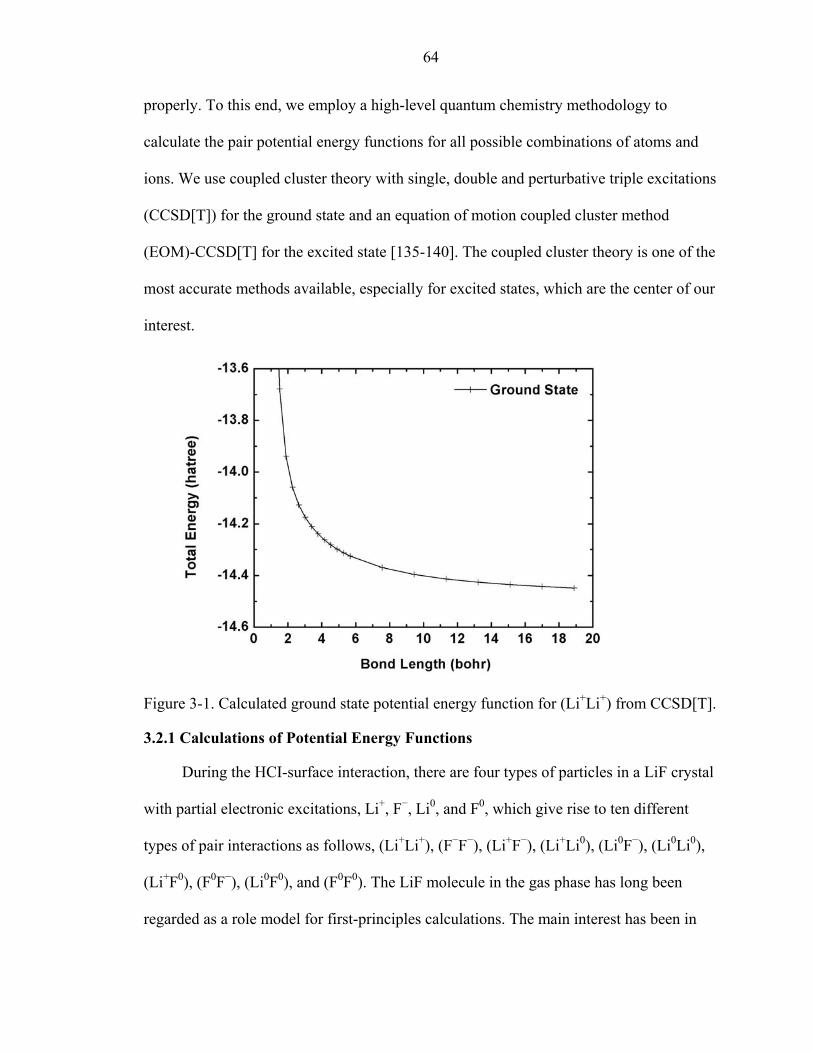
64
properly. To this end, we employ a high-level quantum chemistry methodology to
calculate the pair potential energy functions for all possible combinations of atoms and
ions. We use coupled cluster theory with single, double and perturbative triple excitations
(CCSD[T]) for the ground state and an equation of motion coupled cluster method
(EOM)-CCSD[T] for the excited state [135-140]. The coupled cluster theory is one of the
most accurate methods available, especially for excited states, which are the center of our
interest.
Figure 3-1. Calculated ground state potential energy function for (Li+Li+) from CCSD[T].
3.2.1 Calculations of Potential Energy Functions
During the HCI-surface interaction, there are four types of particles in a LiF crystal
with partial electronic excitations, Li+, F−, Li0, and F0, which give rise to ten different
types of pair interactions as follows, (Li+Li+), (F−F−), (Li+F−), (Li+Li0), (Li0F−), (Li0Li0),
(Li+F0), (F0F−), (Li0F0), and (F0F0). The LiF molecule in the gas phase has long been
regarded as a role model for first-principles calculations. The main interest has been in

65
the nonadiabatic crossing between the potential energy function of the covalent bond
from the excited state and the potential energy function of the ionic bond from the ground
state. A number of calculations have been done since the early 1970s and 1980s using
Hartree-Fock and configuration interaction methods [141-145]. But none of them
provides all the possible ten pair interactions required to model HCI-LiF surface
processes.
Figure 3-2. Calculated ground state potential energy function for (F−F−) from CCSD[T].
To obtain all the potential energy functions needed for simulations, we have
performed state-of-the-art first-principles calculations using the ACES II program [139,
140], which is an implementation of coupled cluster theory. We choose 6-311+G as the
basis set to get the desired accuracy. The calculations are performed on the dimers, which
is a good approximation to the effective potential for LiF crystalline structure (see the
discussion below). For the three pair interactions between two ions, i.e., (Li+Li+), (F−F−),
and (Li+F−), which represent the ground state interactions in crystalline LiF, we have

66
calculated only the potential energy functions of the electronic ground states (see Figure
3-1–3-3). For the other seven pair interactions that involve neutral atoms, which come
from the excited states in crystalline LiF, potential energy functions of the ground state
and at least four low-lying excited states are calculated (see Figure 3-3 to 3-9). Note that
even the ground state of a dimer that consists of a neutral atom and an ion represents an
excited state in crystalline LiF.
Figure 3-3. Calculated potential energy functions for (Li+F−) and (Li0F0) from CCSD[T]. The ground state (crosses) and six low-lying excited states are calculated. Among the excited states, the +Σ (hollow squares) is chosen in the MD simulations.
The potentials for (Li+F−) and (Li0F0) are shown together in Figure 3-3 since they
have the same charge configuration. The accuracies of the binding energy and electronic
excitation energy are 1 meV and 0.1 eV, respectively. This accuracy is acceptable in a
MD simulation since the approximations made in the model lead to larger errors. In
general, the calculations for the closed-shell excited states are more accurate than those

67
for the open-shell; the calculations near the equilibrium distances are more accurate than
those at other distances.
Figure 3-4. Calculated potential energy functions for (Li+Li0) from CCSD[T]. The ground state (crosses) and five low-lying excited states are calculated.
Figure 3-5. Calculated potential energy functions for (Li0F−) from CCSD[T]. The ground state (crosses) and five low-lying excited states are calculated.

68
Figure 3-6. Calculated potential energy functions for (Li0Li0) from CCSD[T]. The ground state (crosses) and five low-lying excited states are calculated.
Figure 3-7. Calculated potential energy functions for (Li+F0) from CCSD[T]. The ground state (crosses) and five low-lying excited states are calculated.

69
Figure 3-8. Calculated potential energy functions for (F0F−) from CCSD[T]. The ground state (crosses) and four low-lying excited states are calculated.
Figure 3-9. Calculated potential energy functions for (F0F0) from CCSD[T]. The ground state (crosses) and five low-lying excited states are calculated.

70
Some features of each of the potential energy functions should be noted. For
interactions (Li+Li+) and (F−F−) (see Figure 3-1 and 3-2), the ground state potentials are
repulsive everywhere as expected, because of the dominant Coulombic repulsion between
two ions of like charge. For the interaction (Li+F−) (see Figure 3-3), the ground state
potential has a region with strong attraction and a 1/ r− tail from Coulombic interaction,
which gives rise to the ionic bonding. For the interaction (Li0F0) (also see Figure 3-3),
which is considered as the excited state of the ionic pair (Li+F−−), all six low-lying excited
states are repulsive everywhere due to covalent anti-bonding. This set of excited states
plays crucial roles in surface processes. For the interaction (Li+Li0) (see Figure 3-4),
potentials of the ground state and the first excited state have regions of attraction, but are
separated by 0.07−0.1 hartree in region (bohr). The next four potentials from
low-lying excited states are repulsive everywhere. For the interaction (Li
04r a>
0F−) (see
Figure 3-5), the potential of the ground state and the five low-lying excited states all have
regions of strong attraction, which lead to one of the unique features in the HCI-LiF
surface dynamics presented below. For the interaction (Li0Li0) (see Figure 3-6), all
potentials have an attractive region, except for the second excited state, which is
repulsive everywhere. For the interaction (Li+F0) (see Figure 3-7), potentials of the
ground state and the first excited state are almost identical; both have regions of weak
attraction. The potential of the second excited state is just above the first excited state
with a region that is slightly repulsive. The next three potentials of low-lying excited
states are approximately 0.4 hartree above the ground state at . For the interaction
(F
04r a>
0F−) (see Figure 3-8), all potentials are repulsive everywhere. For the interaction (F0F0)
(see Figure 3-9), the ground state potential has a very narrow attraction range between
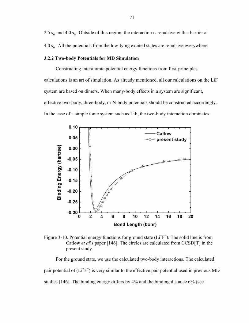
71
2.5 a and 4.0 . Outside of this region, the interaction is repulsive with a barrier at
4.0 a . All the potentials from the low-lying excited states are repulsive everywhere.
0
0
0a
3.2.2 Two-body Potentials for MD Simulation
Constructing interatomic potential energy functions from first-principles
calculations is an art of simulation. As already mentioned, all our calculations on the LiF
system are based on dimers. When many-body effects in a system are significant,
effective two-body, three-body, or N-body potentials should be constructed accordingly.
In the case of a simple ionic system such as LiF, the two-body interaction dominates.
Figure 3-10. Potential energy functions for ground state (Li+F−). The solid line is from Catlow et al’s paper [146]. The circles are calculated from CCSD[T] in the present study.
For the ground state, we use the calculated two-body interactions. The calculated
pair potential of (Li+F−) is very similar to the effective pair potential used in previous MD
studies [146]. The binding energy differs by 4% and the binding distance 6% (see

72
Figure 3-10). Using the calculated pair potential to construct the LiF crystal, we get
7.88 for the lattice constant and 0.37 hartree per pair for the cohesive energy. The
experimental values are 7.58 and 0.39 hartree per pair, respectively [147]. Our results
differ from the experimental values only by 4%. Around the equilibrium position, the two
curves are shifted with respect to each other by nearly a constant, such that the difference
in force constant is almost zero. Since our focus is on the dynamical consequences of the
HCI interaction and the errors in the force constant are negligible, the difference will not
affect the main outcome of the simulation. Beyond the equilibrium position, the
calculated pair potential is more reliable than the effective pair potential, which is not
optimized for long distance interaction.
0a
0a
For the excited states, there is no effective two-body potential derived from first-
principles calculations for extended surface. To date, there is no method yet to treat an
extended system at CCSD[T] level. As an approximation, we use the true two-body (as
contrasted with effective two-body) potentials for a MD simulation. Furthermore, to
simplify the simulations and keep the results tractable, we choose a two-state model, i.e.,
the ground state and one excited state, for MD simulations. We have compared the
oscillator strengths between the ground state and various excited states, and find that low-
lying excited states, in general, have higher strengths than highly excited states. Since, in
the crystalline LiF, the excitation can be more complicated than in dimers, it is reasonable
to take the average of all low-lying states with relatively strong oscillator strengths
instead of using one specific state. On the other hand, the energies among the low-lying
states are close enough such that any one of them will give results similar to those given
by the averaged potential. Also note that for dimers consisting of neutral particles such as
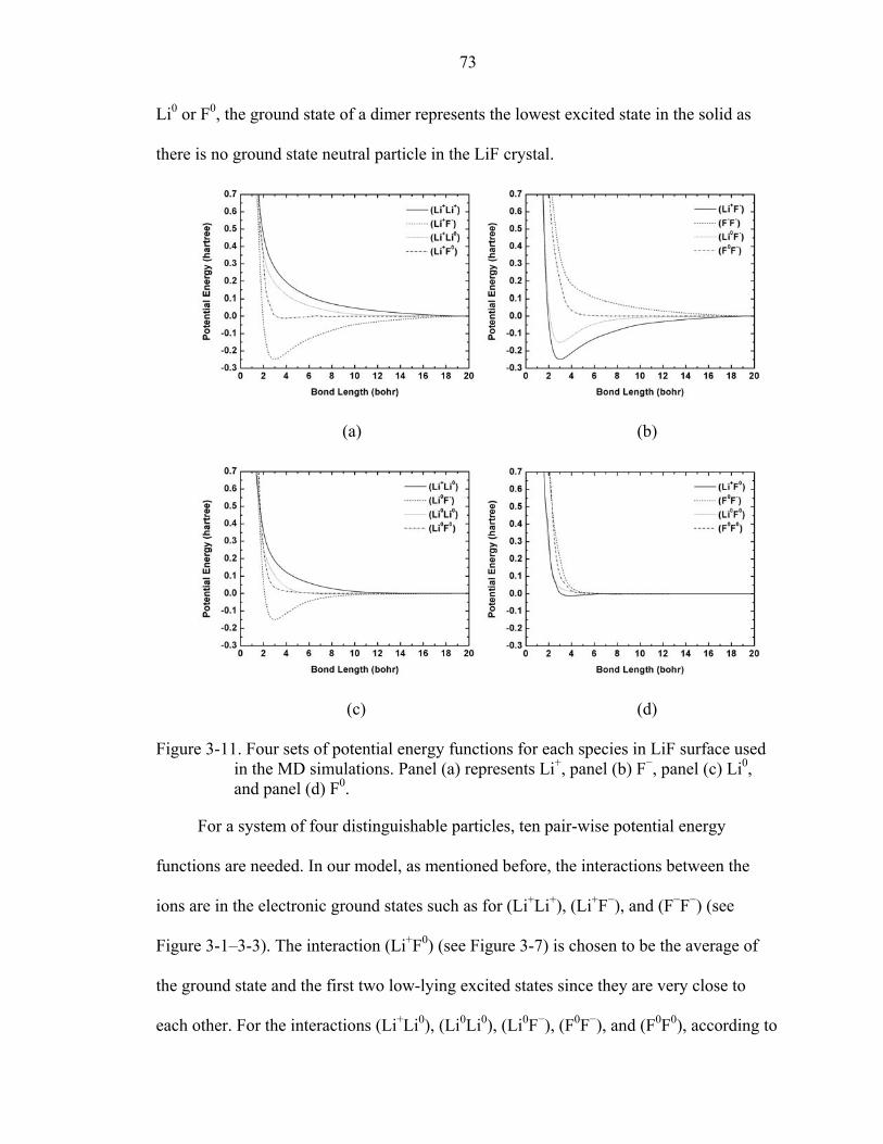
73
Li0 or F0, the ground state of a dimer represents the lowest excited state in the solid as
there is no ground state neutral particle in the LiF crystal.
(a) (b)
(c) (d)
Figure 3-11. Four sets of potential energy functions for each species in LiF surface used in the MD simulations. Panel (a) represents Li+, panel (b) F−, panel (c) Li0, and panel (d) F0.
For a system of four distinguishable particles, ten pair-wise potential energy
functions are needed. In our model, as mentioned before, the interactions between the
ions are in the electronic ground states such as for (Li+Li+), (Li+F−), and (F−F−) (see
Figure 3-1–3-3). The interaction (Li+F0) (see Figure 3-7) is chosen to be the average of
the ground state and the first two low-lying excited states since they are very close to
each other. For the interactions (Li+Li0), (Li0Li0), (Li0F−), (F0F−), and (F0F0), according to

74
the rules mentioned above we take the average values of potentials that are grouped
together and are relatively low-lying. The highest states in Figure 3-8 and 3-9 are
excluded from the selection because of their small oscillator strengths. For (Li0F0), we
include the excited state, as it is known to have a strong transition probability from the
ground state. Consequently, most of the interactions involving excited states are repulsive
everywhere, except for the interaction (Li
+Σ
0F−), which has a very strong attractive region,
and (Li+F0), which has a slightly attractive region.
The potential energy functions as described above are plotted in Figure 3-11. All
curves are shifted slightly such that the energies and forces are zero at large distance in
order to implement them in the MD simulations. In this figure, each panel depicts the
potential energy functions for each type of particle interacting with other three types of
particle and with its own type. A Li+ (see Figure 3-11(a)) is strongly attractive to F− and
strongly repulsive to another Li+. The interaction between a Li+ and a Li0 is repulsive
everywhere, but less strong than an ionic pair of the same charge. The interaction
between a Li+ and a F0 has a very weak attractive region compared to (Li+F−) interaction.
For a F− (see Figure 3-11(b)), the Coulombic interaction with a Li+ is strongly attractive
in the binding region, and repulsive everywhere with another F−. The interaction between
F− and F0 is slightly repulsive at , while the interaction between F04r a> − and Li0 has a
strong attractive feature comparable to the (Li+F−) interaction. When a Li0 (see Figure 3-
11(c)) interacts with a neutral species, F0 and another Li0, the potentials are slightly
repulsive at . It should be noted that a Li04r a> 0 interacts with ions in ways similar to a
Li+ ion. In contrast, a F0 (see Figure 3-11(d)) interacts very differently from its ionic form
F−. All the interactions are quite short ranged and repulsive everywhere, except for a

75
slight attractive region when interacting with a Li+. These features of the potential energy
functions determine the dynamics of the systems as we will discuss in detail in the
following sections.
Figure 3-12. Snapshot of the LiF surface at 0t = for simulation 6. The ions in the topmost two layers are 100% excited. The small darker ball is Li+, the small lighter ball Li0, the large darker ball F−, and the large lighter ball F0.
3.2.3 Simulation Details
The simulation box contains 12,168 particles that are divided into four different
regions (from the bottom to the top of the surface): A static region, a temperature control
region, a dynamical region and a region consisting of excited particles. Both the static
and temperature control region contain two atomic layers (i.e., 1,352 particles). The
lattice constant in our study is 7.88 , as mentioned previously. Periodic boundary
conditions are applied in the
0a
x and directions. Before electronic excitations, the LiF
surface is prepared at room temperature (300 K) with all the particles in their electronic
ground states, i.e., only Li
y
+ and F− ions are present. Thermalization techniques are

76
applied as follows: At first, heat exchange between the system and an external heat bath
is allowed to give all the dynamical particles thermal speeds according to the Maxwell
distribution. Once equilibrium is reached, heat exchange is limited to the temperature
control region just above the static region. These steps are achieved using conventional
classical MD.
The simulation of HCI-surface bombardment begins when a collection of particles
is excited under the influence of the HCI projectile. Each dynamical particle in the
system follows Newton’s equation of motion. In this work, the total potential energy is
the summation of all pair interactions that consist of the ten types of interactions
described in the previous section. The Gear predictor and corrector algorithm [1] is used
to integrate Newton’s equations. The time step is 0.3 fs throughout the simulations. This
time step is found to give very good energy conservation (better than 10−4 for a 103 steps
test run). The total simulation time for most of the runs is approximately 1.2 ps. During
this time period, most important dynamical processes are developed according to our
analysis. Beyond 1.2 ps, the energetic atoms are at distances far away from the surface
that lead to weak interactions. The change in sputtering yields is very small.
3.3 Results and Discussion
3.3.1 Initial Condition
Ten simulation runs were carried out with different excitation configurations; each
represents a possible initial condition. In simulations 1, 2, and 3, 20%, 60%, and 100% of
the ions in the topmost layer are excited, respectively. In simulations 4, 5, and 6, 20%,
60%, and 100% of the ions in the two topmost layers are excited, respectively. In
simulations 7 and 8, 100% of the ions in the three and four topmost layers, respectively,
are excited. In simulations 9 and 10, 100% of the ions in a hemispherical and a
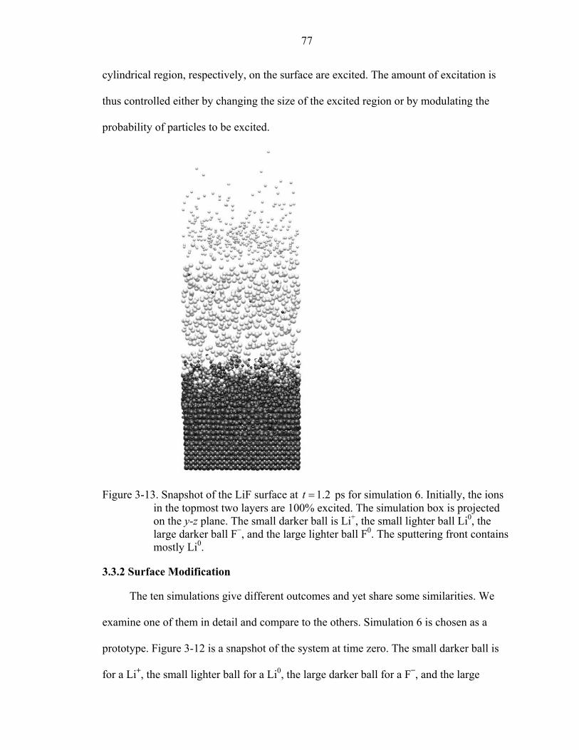
77
cylindrical region, respectively, on the surface are excited. The amount of excitation is
thus controlled either by changing the size of the excited region or by modulating the
probability of particles to be excited.
Figure 3-13. Snapshot of the LiF surface at 1.2t = ps for simulation 6. Initially, the ions in the topmost two layers are 100% excited. The simulation box is projected on the y-z plane. The small darker ball is Li+, the small lighter ball Li0, the large darker ball F−, and the large lighter ball F0. The sputtering front contains mostly Li0.
3.3.2 Surface Modification
The ten simulations give different outcomes and yet share some similarities. We
examine one of them in detail and compare to the others. Simulation 6 is chosen as a
prototype. Figure 3-12 is a snapshot of the system at time zero. The small darker ball is
for a Li+, the small lighter ball for a Li0, the large darker ball for a F−, and the large

78
lighter ball for a F0. The initial condition of excitation in simulation 6 is that the ions in
the two topmost layers are fully excited (i.e., with a 100% probability), so an amount of
potential energy is deposited in the form of electronic excitation. After 1.2 ps, the
potential energy will be released via dynamical processes, which results in surface
modification.
Figure 3-14. Snapshot of the the LiF surface at t 1.2= ps for simulation 9. Initially, the ions in a hemispherical region on the surface are 100% excited. The simulation box is projected on the y-z plane. The small darker ball is Li+, the small lighter ball Li0, the large darker ball F−, and the large lighter ball F0.
The surface modification is depicted in Figure 3-13, which is a snapshot taken at
ps. The shading and sizes of the balls are the same as in Figure 3-13. To get a
better view of the surface modification, the simulation box is projected on the y-z plane.
1.2t =

79
The distinct features of different regions are very clear from the bottom to the top. Right
above the static layers and the temperature control layer are several dynamical layers,
which are about half the thickness of the original simulation box. Atoms in these layers
move very little from their equilibrium, which means that our simulation box is thick
enough to include both the surface and bulk response of the impact of a HCI. Above this
region are the layers close to the surface, where the structure has been very much
perturbed. Most of the particles in this region are ions, depicted in darker shading.
Several Li+ ions in this region try to escape from the surface. Above the surface region,
there are particles sputtered from the surface. Almost all of them are neutral species,
which are depicted in lighter shading. However, the distributions of Li0 and F0 are rather
different. Li0 and F0 are well separated because of the differences in masses, as well as in
the potential energy functions. The topmost region is the sub-region that consists of only
Li0. Between this region and the surface is a spacious sub-region consisting mostly of F0
and very few Li+.
(a) (b)
Figure 3-15. Distribution functions of the number of particles and potential energy along the z direction at 1.2t = ps for simulation 6. Initially, the ions in the topmost two layers are 100% excited. Panel (a) represents the number of particles, and panel (b) the potential energy. In both panels, the solid line represents Li+, the dashed line F−, the dotted line Li0, and the dash-dotted line F0.

80
To compare different initial conditions, we also take a snapshot from simulation 9
at ps (see Figure 3-14). The initial condition for simulation 9 is that the ions in a
hemispherical region on the surface are 100% excited. It can be seen that the distribution
of the atoms sputtered from the surface is quite different from that in simulation 6. There
is not front layer of Li
1.2t =
0 in the z direction.
3.3.3 Sputtering Yield
To analyze these data, a one-dimensional grid is set up along the z direction with
each grid point equally separated in distance. The profiles of physical quantities along the
z direction are calculated by averaging over the x-y plane on each grid point. Figure 3-15
depicts the profile of the number of particles and potential energy for each species at
ps in simulation 6. As seen in Figure 3-15(a), most of the ions stay in the surface,
and the particles that escape from the surface are primarily neutral species. A close
examination indicates that F
1.2t =
0 neutrals are evenly spread out in the z direction in the
region above the surface, in which very few Li+ are present. The distribution of Li0 is
very different from F0. It has two peaks: One is just above the surface and the other is
above the sputtered F0 layers, further away from the surface. These features can also be
seen in the snapshot taken for the same moment in Figure 3-13.
All these features can be understood by the distribution of the potential energy in
Figure 3-15(b). For ions far below the surface, there are strong ionic interactions to bind
them together. The averaged potential looks like a deep square well. This pattern
demonstrates a nearly undisturbed crystal structure. Near the top of the surface, the
potential energy of Li+ ions rises steeply from negative to zero, with small fluctuations
above the surface region. Therefore, a Li+ ion has to overcome a strong attraction to leave
the surface. The potential energy for F− anions oscillates in a deeper negative well near

81
the surface and rises very sharply to zero. This oscillation corresponds to a very perturbed
surface, but the strong attraction from the surface prohibits a F− ion from escaping. The
neutral species only distribute around and above the surface region. The potential energy
for F0 is very small throughout the whole space. It is only slightly negative around the
surface region. These characteristics give rise to the even distribution of F0. Finally, for
Li0, the potential energy has a quite deep dip in the surface region, and a very shallow
negative region in the sputtering front, which corresponds to the two peaks of the Li0
distribution.
To calculate the sputtering yield, we first define the criterion. As shown in
Figure 3-15(b), the potential energies of all the species inside the surface are negative
because the large number of ions acts as an attractive center. As particles move along the
z direction, they feel less and less interaction with other particles, especially with ions,
since ions tend to stay in the surface. The potential energies eventually become zero at
, which suggests that it is reasonable to set the escape distance to be in this
case.
040z = a 040a
According to this criterion, the numbers of particles that are sputtered out of the
surface in simulation 6 are seven Li+, 0 F−, 342 Li0 and 465 F0. The mass-sputtering yield
for neutral species is 99.6%. Table I shows the initial conditions and respective sputtering
yields for all ten simulations. It can be seen that with the same number of layers,
increasing the probability of initial excitation can dramatically increase the neutral mass-
sputtering yield. When only a monolayer is excited, the neutral mass-sputtering yields are
64.6%, 71.2%, and 99.1% for the initial conditions, in which 20%, 60%, and 100% of the
ions are excited, respectively. When two layers are involved, the neutral mass-sputtering
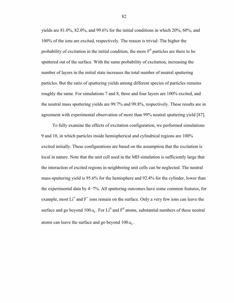
82
yields are 81.0%, 82.0%, and 99.6% for the initial conditions in which 20%, 60%, and
100% of the ions are excited, respectively. The reason is trivial: The higher the
probability of excitation in the initial condition, the more F0 particles are there to be
sputtered out of the surface. With the same probability of excitation, increasing the
number of layers in the initial state increases the total number of neutral sputtering
particles. But the ratio of sputtering yields among different species of particles remains
roughly the same. For simulations 7 and 8, three and four layers are 100% excited, and
the neutral mass sputtering yields are 99.7% and 99.8%, respectively. These results are in
agreement with experimental observation of more than 99% neutral sputtering yield [87].
To fully examine the effects of excitation configuration, we performed simulations
9 and 10, in which particles inside hemispherical and cylindrical regions are 100%
excited initially. These configurations are based on the assumption that the excitation is
local in nature. Note that the unit cell used in the MD simulation is sufficiently large that
the interaction of excited regions in neighboring unit cells can be neglected. The neutral
mass-sputtering yield is 95.6% for the hemisphere and 92.4% for the cylinder, lower than
the experimental data by 4−7%. All sputtering outcomes have some common features, for
example, most Li+ and F− ions remain on the surface. Only a very few ions can leave the
surface and go beyond 100 . For Li0a 0 and F0 atoms, substantial numbers of these neutral
atoms can leave the surface and go beyond 100 . 0a

83
Table3-1. Sputtering yields of ten MD simulations with different initial conditions.
Configuration One layer Two layers Three layers Four Layers Hemisphere Cylinder
Probability (%) 20 60 100 20 60 100 100 100 100 100
Simulation 1 2 3 4 5 6 7 8 9 10
Li+ 0 10 5 2 21 7 3 7 2 4
F− 1 14 1 1 13 0 1 0 2 6
Li0 5 35 34 1 8 342 433 470 19 33
F0 0 31 288 7 91 465 616 865 53 78
Neutral mass yield (%) 64.6 71.2 99.1 81.0 82.0 99.6 99.7 99.8 95.6 92.4

84
This picture of dominant neutral sputtering yield is expected from the DMS
model [87, 101, 102, 108, 112, 123, 124]. At the surface, H-centers decay by emitting F0
atoms and F-centers neutralize Li+ cations. The newly created neutral Li0 atoms at the
surface form a metallic layer, which is stable at room temperature, but will evaporate at
increased temperature. Since these Li0 atoms are weakly bound to the surface, when a
HCI approaches the surface, which is not included explicitly in our simulations, the
momentum transfer will be large enough to sputter these Li0 atoms out the surface as a
retarded sputtering effect [87, 101, 102, 108, 112, 123, 124].
Figure 3-16. Distribution functions of the kinetic energy along the z direction at t 1.2= ps for simulation 6. Initially, the ions in the topmost two layers are 100% excited. The solid line is for Li+, the dashed line F−, the dotted line Li0, and the dash-dotted line F0.
The sputtering outcome can only be understood in depth by examining the features
of the potential energy functions. The formation of a layer of Li0 atoms on top of the
surface is the result of the attraction in the (Li0F−) potential energy function (see

85
Figure 3-5). The everywhere-repulsive feature of the other potential energy functions that
involve neutral atoms determines the dominant sputtering of the neutral atoms.
So far, the simulations results have demonstrated two key characteristics of the
DMS model: First, the sputtering yield is dominantly neutral; and second, there is a layer
of Li0 atoms bound to the surface. We believe that this layer of Li0 atoms can be sputtered
out of the surface if a sufficient momentum transfer from the projectile ions to the atoms
can be realized.
Figure 3-17. Normalized angular distribution functions of the neutral particles averaged over simulations 3, 6, 7, and 8 at 1.2t = ps. The solid line represents Li0, the dashed line F0, and the dotted line the total neutral particles.
3.3.4 Profile of Dynamics
In order to obtain a full, quantitative description of the HCI-LiF surface dynamics,
we present the distribution functions of kinetic energy along the z direction. The same
one-dimensional grid is used as for the number of particles and potential energy in
Figure 3-15. Again, results from simulation 6 are used to illustrate the analysis. As shown

86
in Figure 3-16, most of the kinetic energy of the system is carried by the particles
sputtered out of the surface. The ions far below the surface region only have very little
kinetic energy. The kinetic energy of both Li+ and F− increases at the surface. For the
very few Li+ ions that have successfully escaped from the surface, the kinetic energy is
higher than the Li+ in the surface. For Li0 and F0 neutrals, the kinetic energy in the z
direction increases as a function of distance. The fastest particles are the sputtered
particles in the front. In addition, kinetic energies of Li0 neutrals also have strong peaks
around the surface region, which are from the Li+ remaining on the surface, but with
smaller magnitudes compared to the sputtered atoms. The magnitudes are comparable to
that of F−. In the surface region, the fastest particles are Li0 and F−.
Figure 3-18. Distribution functions of the number of particles and potential energy along the z direction of Li0 at different time instants for simulation 6. Panel (a) represents the number of particles, and panel (b) the potential energy. In both panels, the solid line is for 0.006t = ps, the dashed line for t ps, the dotted line for ps, and the dash-dotted line for ps.
0.042=1.2000.600t = t =
The next question is the angular distribution of the sputtered atoms due to the
escaping velocity. A complete analysis of all ten simulations indicates that full-layer
excitation, i.e., 100% ions in the top surface layers, has the feature of nearly vertical back
scattering. The averaged angular distribution functions of the sputtered atoms from
simulations 3, 6, 7, and 8 are presented in Figure 3-17. The maxima of the angular
87
distribution are located closely at zero degree because of the repulsion among the excited
particles. For partial-layer excitation or localized excitation, the angular distribution does
not have a sharp peak near zero degree. These results suggest that angular distribution
functions can be used, in conjunction with sputtering yields, to determine the geometry
and nature of initial excitation when compared to experiments.
To obtain a picture of how these features have been developed through time, we
analyze the distributions of the number of particles and potential energy for Li0 and F0 as
functions of time from simulation 6. In Figure 3-18 and 3-19, these physical quantities
are shown at four instants, t 0.006, 0.042, 0.6, and 1.2 ps. At the beginning of the
simulation, all Li
=
0 neutrals are evenly distributed in the topmost two layers (see Figure 3-
18(a)). These Li0 have very high positive potential energy (see Figure 3-18(b)). The
potential energy of the Li0 neutrals in the surface region decreases dramatically in the
first 0.6 ps, from positive to negative.
(a) (b)
Figure 3-19. Distribution functions of the number of particles and potential energy along the z direction of F0 at different times for simulation 6. Panel (a) represents the number of particles, and panel (b) the potential energy. In both panels, the solid line is for t ps, the dashed line for t0.006= 0.042= ps, the dotted line for ps, and the dash-dotted line for 0.600t = 1.200t = ps.

88
As time evolves, the Li0 neutrals gain kinetic energy and lose potential energy.
Very shortly, around 0.042 ps, the single peak for the distribution starts to split into two
peaks, as shown in Figure 3-18(a) by a dashed line. The main peak near the surface does
not move as much as the front peak in the z direction, which eventually separates entirely
from the main peak around 0.6 ps. Later, the front peak continues its motion in the z
direction with high velocity while maintaining a similar shape, which can be seen from
the profiles at 0.6 and 1.2 ps. During the simulation, there is always a substantial amount
of Li0 neutrals on the surface. The Li0 neutrals in the front peak are the fastest particles
due to the small mass of a Li0 compared to a F0.
In contrast to Li0, the profile of F0 does not change much at 0.042 ps when the
profile of Li0 starts to split into two peaks (see Figure 3-19(a)). As time evolves, the
potential energy of F0 decreases to slightly negative (see Figure 3-19(b)). The distribution
of F0 spreads in time and becomes evenly distributed over z during the simulation, as can
be seen at 1.2 ps in Figure 3-19(a).
Similar analyses of the other nine simulations indicate that when the excitation
probability exceeds 60% of the excited region, there will always be a Li0 enriched surface
layer as a consequence of HCI-LiF interaction. This characteristic vanishes at low
excitations, i.e., when only 20% of the ions in the surface layer are excited initially.
Therefore, the neutral Li0 layer alone is not a sufficient condition to determine the nature
of excitation, i.e., local vs extended. However, the combination of this feature with
neutral/ion ratios in sputtering yields and angular distribution of the sputtered particles
can pinpoint the problem.

89
3.4 Conclusion
In this chapter, we have thoroughly investigated the possible outcomes during HCI-
LiF surface interactions, which display unique characteristics among the HCI-surface
bombardment. We have constructed potential energy functions from first-principles
calculations, which govern the dynamics and energetics of particle-surface interactions. A
one-to-one mapping between the initial condition and the sputtering outcome has been
established to determine the nature of sputtering. Our results demonstrate that the higher
the percentage of the excited ions in the surface layers, the higher the percentage of
neutral sputtering particle yields in the final state. In most of the simulations, the surface
after bombardment is Li0-enriched, which is in good agreement with the DMS model [87,
101, 102, 108, 112, 123, 124]. It is found that the 100%, extended surface excitation
(simulations 3, 6, 7, and 8) generate results that are close to the published experimental
observations of more than 99% neutral particle sputtering yields [87]. Our analysis
indicates that the strong attraction of (Li0F−) is the dominating factor for forming a Li0
neutral layer on the surface. The everywhere-repulsive feature of the other potential
energy functions that involve neutral atoms determines the dominant neutral sputtering
yield. Although some of important processes, such as Auger cascades, resonant states,
and neutralization of ions are not included explicitly in our simulation model, crucial
effects on lattice dynamics from these processes are included via different excitation
configurations. Overall, we have made progress towards understanding the extremely
complex dynamics of nuclei by including electronic excitation, and by correlating the
initial state with the final state.

CHAPTER 4 AN EMBEDDING ATOM-JELLIUM MODEL
4.1 Introduction
In the jellium model, nuclei and core electrons together are replaced by a uniform
positive background. Valence electrons move quantum mechanically in the field of this
positive background. Using jellium to model a metal dates back to Drude’s work on free
electron conductance. The jellium model is also the simplest model to calculate the
electronic structure of metal surfaces as demonstrated by Bardeen [148]. Lang and
Kohn [149-151] were the first to do self-consistent calculations using the jellium model
within DFT to study the properties of metal surfaces. They treated a metal surface as a
semi-infinite jellium and explored the two-dimensional translation symmetry to set up a
one-dimensional KS equation in the direction perpendicular to the jellium surface. In a
sequence of papers [150-153], Lang and Kohn studied the surface energy and work
function of different metal surfaces characterized only by the Wigner electron sphere
parameter sr . They found that, within the jellium model, the work function can be
reasonably well described for metal of all density range, while the surface energy is
negative for a high density metal. With the introduction of ionic effects in a simple
pseudopotential treated as a first order perturbation, the negative surface energy is
corrected and the work function is improved. This idea is further pursued in Perdew et
al.’s stabilized jellium or structureless pseudopotential model [154-156], liquid drop
model [157], and Shore and Rose’s ideal metal model [158-161].
90
91
It is not a surprise that the jellium model also was used in the pioneering work of
atomic adsorption on metal surfaces studied by Grimley et al. [162], Lang and
Williams [163, 164], and Gunnarsson et al. [165] In their atom-jellium model, Lang and
Williams [163, 164] described the substrate as a semi-infinite jellium and solved self-
consistently a Dyson equation, which couples the Green’s function of the bare jellium
surface with the electrostatic potential due to the adsorbate atom. The latter is treated as a
perturbation to the bare jellium surface. Lang and Williams studied a group of atoms
chemisorbed on a high density metal surface ( r 2.07s = ) like Al. Although the model is
simple, it gives the correct picture of the qualitative difference among different types of
chemisorption. They elaborated the difference in detailed analysis of density of states,
charge transfer, and work function changes, which became a standard routine followed by
a large number of subsequent first-principles DFT studies of surface adsorption. Later,
the same atom-jellium model strategy was used by Price and Halley [166] in a three-
dimensional repeated supercell approach and many others [167].
During the past decade, with the developments in first-principles pseudopotentials,
iterative minimization algorithms and computer hardware, accurate and sophisticated
DFT calculations of adsorption system with atomic surface became the choice, and the
jellium model of metal surface seems outdated. However, the jellium model still has the
advantage of numerical efficiency and can be taken as the simplest pseudopotential. Here
we propose to extend Lang and Williams’s atom-jellium model and combine the
advantages of both atomic and jellium model in a multiscale sense to study molecular
adsorption on metal surfaces. In our approach, the most important interface region, which
includes the top metal layers and the adsorbate molecule, is described in the accurate

92
atomic pseudopotential. This region is embedded in a jellium region, which is far enough
from the interface region, that its rough description is acceptable. In doing so, the
computational cost should be lowered without critical loss of accuracy.
4.2 DFT Formulism for Embedding Atom-jellium Model
In our approach, part or all of the metal surface is modeled by a jellium slab as a
uniform positive background, which occupies a certain volume jelΩ in the surface unit
cell. The charge density of the jellium slab is
( )0 .
jeljel
n forn
otherwise+ ∈Ω
=
rr (4-1)
The parameter corresponds to the average charge density of valence electrons in the
metal. In Drude’s theory of free electron systems, an electron is defined by the volume it
occupies
n+
( )4 3 3srπ , where sr is the classical radius of the electron. As for a fcc metal,
assuming Z valence electrons for each metal atom, there is a simple relation
3
21 43 4s
arn Z
π
+
= = , (4-2)
where is the lattice constant. a
Again, we use pseudopotentials to describe the interaction between ions and
electrons, and a plane wave basis set with a three-dimensional periodic boundary
condition. With electrons, ions and a jellium slab, the total energy functional in DFT is
( ) ( ) ( )
( ) ( ) ( )
( ) ( ) ( )( ) ( ) ( )
0
23
, , ,, 2
, .
xc es
i i i xci
H pp ion ion I
el jel ion jel I jel jel
E T n E n E n
w f d r E n
E n E n E
E n E n E n
ψ ψ∗
−
− − + −
= + + ∇
= − +
+
+ + + + + +
∑ ∫k k k kk
r r r
r r
r r R
r R
r (4-3)

93
The only difference from the conventional DFT expression in the pseudopotential
approach is the electrostatic energy , which now includes the contributions from the
jellium slab. Among them, and are constant for a fixed geometry
configuration because they are independent of electron density . But these two terms
need to be evaluated correctly in the total energy, which in turn will allow the correct
Hellmann-Feynman force calculation. The self-consistent Kohn-Sham equation is
esE
ion jelE − jel jelE −
( )n r
( ) ( ) ( ) ( ) ( ) ( )2
, , ,2 xc H pp jel i i iV V V V ψ ε ψ ∇− + + + + =
k k kr r r r r r , (4-4)
where the jellium potential
( ) ( )3 jeljel
nV d r′= −
′−∫r
rr r
(4-5)
is the Coulomb interaction between the positive jellium slab and electrons.
Following the formalism of total energy calculation with three-dimensional PBC in
Appendix A, we can cast the energy between electrons and jellium into a reciprocal space
expression
( ) ( ) ( )
( ) ( ) ( )
( ) ( )
( ) ( )
( ) ( )
3 3
3 32
0
3 32
0
20
0
,
4 1
4 1
4
,
el jel jel
ijel
ijel
jel
jel
E d r n d r n
d r n d r n e
d r n e d r n e
n n
V n
ηχ
π
π
π
− Ω Ω →∞
′−
Ω Ω≠
′−
Ω Ω≠
∗
≠
∗
≠
′ ′ ′ = −
′ ′= − Ω
′ ′= − Ω
= −Ω
= −Ω
∫ ∫
∑∫ ∫
∑ ∫ ∫
∑
∑
G r r
G
G r G r
G
G
G
r r r r
r rG
r rG
G GG
G G
i
i i i (4-6)
where

94
( ) ( )24
jel jelV nπ=G G
G (4-7)
is the Fourier transform of the jellium potential ( )jel rV . Similarly, the energy between
jellium and itself is
( ) ( ) ( )
( ) ( )
3 3
0
1 ,2
.2
jel jel jel jel
jel jel
E d r n d r n
V n
ηχ− Ω Ω →∞
∗
≠
′ ′ ′ =
Ω=
∫ ∫
∑G
r r r r
G G (4-8)
Because the interaction between the ions and the jellium is also straightforward
Coulombic repulsion, the energy between them can be expressed as
( ) ( ) ( )
( ) ( )
( ) ( )
3 3
3 32
0
20
,
4 1
4 ,
ion jel jel I II
i ijel I I
I
jel
E d r n d r Z
d r n e d r Z e
S n
η
δ χ
π δ
π
− Ω Ω→∞
′−
Ω Ω≠
∗
≠
′ ′ ′ = −
′ ′= −Ω
= Ω
∑∫ ∫
∑ ∑∫ ∫
∑
G r G r
G
G
r r R r r
r rG
G GG
i iR (4-9)
where
( ) IiI
I
ZS e− = Ω ∑ G RG i (4-10)
is the structure factor of the ions. Finally, the force exerted on the ions due to the jellium
is
( )
( )20
4 ,I
ion jelion jel I
I
iIjel
E
Zi e nπ
−−
− ∗
≠
∂= −
∂
= Ω Ω ∑ G R
G
F RR
G GG
i (4-11)
which will be added to all the other contributions from electrons and ions.
The embedding atom-jellium method has been implemented in code of
fhi98md [168], which uses Troullier-Martins type norm-conserving pseudopotential to
describe the interaction between ions and electrons.

95
4.3 Results and Discussion
In Figure 4-1, the planar averaged electron density and potential are plotted in
direction perpendicular to the (111) surface for a seven-layer Al jellium slab. The
electron density fluctuates around the jellium edge and smears out into vacuum as seen in
Figure 4-1(a). The fluctuation amplitude is reduced as the center of the positive jellium
background is approached. This fluctuation in electron density has the characteristic of
Friedel oscillation, which corresponds well with the electrostatic and total effective
potentials shown in Figure 4-1(b). The electron exchange-correlation contributions
lowers the potential effectively.
z
(a) (b)
Figure 4-1. A jellium surface modeled by a seven-layer Al slab with 21 electrons.(a) Charge density along the direction perpendicular to the jellium surface, the solid line is the positive jellium charge density, the dashed line is the electronic charge density. (b) Potentials in the same direction, the solid line is the total effective potential, the dashed line is the part without the exchange correlation potential.
The physical properties of metal thin film subjects to static quantum size effect
(SQSE). As first shown by Schulte [169] and subsequently others [170-176], this is
because the surface bands are shifted down to touch the Fermi level one by one as the
thickness of the slab increases. When an empty band touches the Fermi level, the work

96
function reaches a local minimum. The SQSE is more severe for a jellium slabs than for a
real metal thin film. The work function SQSE for jellium Al and Cu slab is shown in
Figure 4-2(a) and (b), respectively. The work function converges to 3.78 eV for jellium
Al and 3.55 eV for jellium Cu, as indicated by the horizontal dashed lines in Figure 4-2.
The work functions calculated from an unrelaxed seven-layer atomic slab are also shown
as the horizontal solid lines at 4.21 eV and 5.19 eV for Al and Cu, respectively.
(a) (b)
Figure 4-2. The quantum size effect of jellium surfaces, (a) Al and (b) Cu. The dashed line corresponds to the converged work function for simple jellium model. The solid and dotted line are the work functions calculated from the atomic model and the embedding atom-jellium model, respectively.
To improve the results from the pure jellium model, we introduce the embedding
atom-jellium model by placing one atomic layer on a six-layer jellium slab. The distance
between the atomic layer and the jellium surface is relaxed to give the lowest energy. The
equilibrium distance is 1.7 Å and 1.5 Å for Al and Cu, respectively. In Figure 4-2, the
dotted lines show that the work function for the embedding atom-jellium model is 4.22
and 4.93 eV for Al and Cu, respectively. The improvement of the embedding atom-
jellium model over the pure jellium model is significant.

97
The good agreement between the EAJ model and atomic model can be understood
by examining the electronic structure. In Figure 4-3, the partial density of states projected
on the first Al layer of atomic and EAJ model, and the second Al layer of the atomic
model are shown. The PDOS of the first Al layer of EAJ model matches well with that
from the atomic model. For the second Al layer, the PDOS of px, py and pz are all the
same. For first Al layer, pz orbital contributes more states around the Fermi level than px
and py.
Figure 4-3. Partial density of states projected on atomic orbitals. (a) The first Al layer in the embedding atom-jellium model. (b) The upper and lower panel is for the first and second Al layer in the atomic model. The Fermi level is at the energy of zero.

CHAPTER 5 FRACTURE AND AMORPHIZATION IN SIO2 NANOWIRE STUDIED BY A
COMBINED MD/FE METHOD
5.1 Introduction
In the past decade, multiscale modeling has emerged in computational material
science [177]. It combines models at different physical scales to build a comprehensive
description of materials. The reason to do multiscale modeling is two-fold. First, there is
a variety of phenomena that are strongly coupled in different physical scales. For
example, in crack propagation, the bond breaking at the crack tip depends on the
deformation of surrounding materials, which in turn depends on the long range strain
field. On the other hand, the dissipation of strain energy is through dynamical processes
at the crack tip including bond breaking, plastic deformation, and emission of elastic
waves. All of these processes happen at the same time when crack propagates. So a
successful description of crack propagation requires simultaneous resolution at both
atomistic and continuum length scales. Secondly, it is not possible to compute all the
relevant dynamical processes in the most accurate and intensive model with a reasonable
computational cost. The idea of multiscale modeling is to find a balance between
accuracy and efficiency, i.e., let the most dramatically changing region be dealt with via
the most accurate method and broad surrounding regions dealt with by less accurate but
more computationally efficient methods.
The multiscale scheme of combining molecular dynamics (MD) and the finite
element (FE) method has been studied by many researchers to investigate fracture and
98

99
crack propagation in materials. One group of studies focuses on deriving the FE method
not from the traditional continuum model, but from the underlying atomistic model. In
the quasicontinuum technique proposed by Tadmor, Phillips and coworkers [178-181],
the energy of each element is computed from an underlying atomistic Hamiltonian, such
that nonlinear elastic effects can be included. In the coarse-grained molecular dynamics
proposed by Rudd and Broughton [182], a similar idea is pursued. The interpolation
functions in the FE mesh are assembled from the atomistic model. The other group of
studies focuses on combining MD and FE through an interface. Kohlhoff et al. [183]
introduced an interface plane between the MD and FE regions to pass the displacement as
boundary conditions for the two regions. Abraham et al. [184-186] used a scheme based
on coupling through force. In it, the FE elements sitting at the interface plane can have
forces of MD nature. Smirnova et al. [187] extended the imaginary interface plane to a
finite size. In this work, we propose an improved MD/FE interface with gradual coupling
of force and use it to study the mechanical behavior of a SiO2 nanowire.
SiO2 is one of the most extensively studied materials because of its importance in
technology. Amorphous silica is the major constituent in optical fiber. Quartz is the
material for timing in electronic circuits. Other crystalline silica, such as cristobalite, can
be found in Si and SiO2 interface in microchips [188, 189]. Since the discovery of carbon
nanotubes, different types of nanotubes and nanowires have been studied both in theory
and experiment. For example, a SiSe2 nanowire has been proposed and studied with
MD [190-192]. In experiments, both SiO2 sheathed Si nanowires [193] and pure SiO2
nanowires [194-196] have been found. SEM and TEM images show that the nanowires
are several µ m long with diameter of 10-50 nm. Electron diffraction on SiO2 sheathed Si

100
nanowire shows that the core of the nanowire is crystalline Si and the outmost cover is
amorphous SiO2. In pure a SiO2 nanowire, the structure is also amorphous. While the
structures of crystalline silica are well understood as different arrangements of corner-
sharing SiO4 tetrahedral, the structure of the amorphous silica surface is still an open
problem [197, 198]. Since we do not have a well-defined structure for the amorphous
SiO2 nanowire to start with, a closed crystalline structure should be used. Besides
amorphous structure, silica can have as many as forty crystalline structures in
nature [199]. Among these different silica polymorphs, only quartz (α β, ) and
cristobalite (α β, ) are stable at atmospheric pressure. The density of β -cristobalite is the
closest to that of amorphous silica. So β -cristobalite is often used as a preliminary model
for amorphous silica. As the first step to understand the mechanical properties of an
amorphous SiO2 nanowire, we construct a α -cristobalite nanowire and use the combined
MD/FE method to study its amorphization and fracture under tensile stretch. As we will
demonstrate, during the first period of tensile stretch, a phase transition occurs from α -
cristobalite to β -cristobalite. With further tensile stretch, the nanowire become
amorphous before it starts to fracture.
5.2 Methodology
5.2.1 Summary of Finite Element Method
The finite element method is a general approach to solve a differential equation
approximately [200]. A continuous system has infinite degree of freedom. The FE
method uses finite degree of freedom to approximate the continuous solution. When a
continuous system is divided into a finite element mesh, the displacement field
101
( )cu r within an element can be interpolated by the local displacement on the nodes of
that element u as ei
( ) ( )1
gNc e
i ii
H=
= ∑u r r u , (5-1)
where is the interpolation function or shape function. The index runs from one
to
( )iH r i
gN , the number of nodes in each element. The continuous strain within an element can
be symmetrically defined as [201],
( ) ( ) ( ),
1
112
gNi ic e
ii
H Hu u
r r ,eiµν µν µ
ν µ
ε δ=
∂ ∂ = − + ∂ ∂ ∑
r rr ν , (5-2)
where all quantities are written out in their components and the indices µ and ν run
from one to fN , the degrees of freedom of each node. The equations above are usually
expressed in matrix format
( ) ( )c e=u r H r u , (5-3)
and
( ) ( )c e=ε r D r u , (5-4)
where the local displacement is written as a vector of eu g fN N× dimensions. The
matrix is the strain-displacement matrix as defined from Eq.5-2. ( )D r
In solid mechanics, the FE method is introduced as a minimization of the total
potential functional [200]
12
T T T
Sd dπ
Ω Ω= Ω+ Ω+∫ ∫ ∫σ ε u p u qdS , (5-5)

102
where σ is the stress, is the body force per unit volume and q is the applied surface
force per unit area. The FE method often deals with elastics, which means small strain,
harmonic and no plasticity. The stress-strain relation is linear
p
= =σ Cε CDu , (5-6) where C is the elastic matrix. As the system is divided into a finite element mesh, the
elastic potential energy functional can be written as
1 .2 e e e
e
e
eT T e eT T eT T
Se
d d
π π
Ω Ω
=
= Ω+ Ω+
∑
∑ ∫ ∫ ∫u D CDu u H p u H q dS (5-7)
To find the minimum of the total potential energy and the equilibrium of the system, the
variational principle is used,
0 ( )e e
T e T Te S
d de
dSπΩ Ω
∂ = = Ω + Ω+ ∂ ∫ ∫ ∫D CD u H p H qu
. (5-8)
This gives
0e e e+ =K u F , (5-9) where
e
e T dΩ
= Ω∫K D CD (5-10)
is the local stiffness matrix and is the nodal force that results from the last two terms
in Eq.5-8. There are as many as equations like the one in Eq.5-9, since is the total
number of elements in the system. These equations are coupled through u . They can be
assembled as one global matrix equation,
eF
eN eN
e
0+ =Ku F , (5-11) where K is the global stiffness matrix and is the generalized displacement matrix. u

103
Up to this point, we only get the equation for elastic statics, which is the most
common application of the conventional FE method. To consider elastic dynamics, we
have to introduce kinetic energy for an element,
( ) ( )
( ) ( )( )
212121 ,2
e
e
e e
Te
eT e e
T d
d
ρ
ρ
Ω
Ω
= Ω
e= Ω
=
∫
∫
r u r
Hu r Hu
u M u
(5-12)
where
( )e
e T dρΩ
= Ω∫M r H H (5-13)
is the local mass matrix. If we construct the Lagrangian and use the variational principle
as before, a global dynamical equation can be obtained
0+ + =Mu Ku F . (5-14) With the condition of no external force and no boundary condition, the equation turns to
the free response,
0+ =Mu Ku . (5-15) The harmonic solution (0) i te ω=u u gives an eigenvalue equation
2 0ω− + =M K , (5-16) which is just the same as the dynamical matrix equation for a crystal lattice [202]. With
the condition of no external force and strain applied on the boundary of the system, the
dynamical equation is now
= −KuuM
. (5-17)

104
Generally, M is non-diagonal and is called the consistent-mass matrix. With a set of
interpolation functions satisfying
T =H H I , (5-18)
M is diagonal and is called the lumped-mass matrix.
The dynamical equation can be solved in the central difference method (Verlet) or
Newmark’s method [200]. The former is explicit and very computationally efficient when
applied with lumped-matrix approximation. It acts just like Hooke’s law for each
individual node. The later is numerically more stable. But it involves solving matrix
equation implicitly and so more computationally demanding.
5.2.2 Hybrid MD/FE: New Gradual Coupling
In our approach, the system is divided into three regions, i.e., core MD (CMD),
dilute FE (DFE) and transition (TRN) region. FE nodes in the TRN region match the
crystal lattice. The total Hamiltonian of the system is
( ) ( )( ) ( ) ( ) ( ) ( )( ) ( ) ( )
/
/
, /
, /
, , .
tot CMD CMD TRN
DFE DFE TRN
TRN
H H CMD V CMD TRN
H DFE V DFE TRN
H TRN
= ∈ + ∈
+ ∈ + ∈
+ ∈
r r r
u r u r u r
u r u r r
(5-19)
In , CMDH DFEH and , we include the kinetic energy from each region and the
contribution of the potential energy between any two particles or connecting nodes if they
both are in the same region. In V and
TRNH
/CMD TRN /DFE TRNV , we include the interaction between
two particles or connecting nodes which are in nearby, different regions. Inside the TRN
region, we have
( ) ( ) ( ) ( )( ) ( ) (( ) ( )( )
, ,
1 ,
MDTRN TRN
FE
H TRN T w
w V
∈ = +
+ −
u r u r r u r r r
r u r
)V (5-20)

105
where the weight function, ( )w r , is determined by the distance of the nodes from the
CMD and DFE regions. When the force is calculated between two FE nodes in the TRN
region, we allow the MD force between them to contribute. The weight of such a
contribution of MD nature is determined by the distance of the nodes from the CMD and
DFE regions. So the hybrid force in the TRN region can change from the nonlocal MD
force where the nodes are very close to the CMD region to the local FE force where the
nodes are close to the DFE region.
The interatomic potential we use for MD is due to van Beest et al [203]. It was
generated by fitting the results of a Hab initio 4SiO tetrahedron and the experimental
crystalline data to the following formula,
4
( ) 6s s iji j i ji j
i j
b rs s sij s s
ij ij
q q Cr A e
r rυ
−= + −
s , (5-21)
where is the species of the ith particle. The potential has been intensively used in MD
simulations of bulk silica and is commonly called the BKS potential.
is
We use a two-dimensional FE method by dividing the system into isoparametric
triangular elements with linear interpolation functions. The number of nodes for each
element and the degree of freedom of each node 3gN = 2fN = . The total number of
elements and nodes is and , respectively. The potential energy is eN dN
6
, 1
12
eNFE m m m
p pq qm p q
V u=
= ∑ ∑ K u , (5-22)
and the stiffness matrix is
[ ] [ ]4
Tm mm
LK D CA
mD = , (5-23)

106
where is the thickness in the reduced dimension and is the area of the element. In a
two-dimensional system, the elastic constant matrix, [ , is reduced to as
L mA
]C (3 3)×
[ ]11 12
12 11
14
00
0 0
C CC C C
C
= . (5-24)
The strain-displacement matrix [ consists of coordinate differences of the nodes on
each element. It is of the dimension
]D
(3 6)× . The force on each element is
m mp pqF K u= m
q , (5-25)
where the index of p and runs from one to six. It is desirable to decompose the force
on each node as
q
3
1
e
l
Nn m
i nm l
F δ=
=∑∑ m pF , (5-26)
where the index of runs from one to two. The kinetic energy is i
6 2
1 1
12
e dN NFE m nm m
p qpqm p q n
T Mu u, = =
= =∑ ∑ ∑ unM , (5-27)
and the mass matrix is
3
1 1 3
e
l
Nn m
nmm l
AM Lρ δ= =
= ∑∑ , (5-28)
where ρ is the bulk density of the material and we have used the lumped-mass
approximation. After the forces are calculated from different contributions, we use the
Verlet algorithm to integrate the dynamical equations for both MD and FE.
5.3 Results
The nanowire sample that we use is shown in Figure 5-1. The dimensions are 19.91
, 27.79 and 119.47 Å in the x , and direction, respectively. The strain will be applied y z

107
on the direction. The projection from MD particles to FE nodes in the TRN region is
in the direction as shown in Figure 5-1(b). To construct the nanowire, we use the 12-
basis unit cell for
y
z
α -cristobalite with the dimension of 4.978×4.978×6.948 Å. The
CMD region has 4×8×4 unit cells with 1536 particles. Each of the TRN regions has
4×4×4 unit cells. It has the dimension larger than the cut off of the BKS potential. Each
FE node in the TRN region corresponds to four MD particles in different layers. The
TRN regions have 384 FE nodes, which correspond to 1536 MD particles. The two DFE
regions have 32 FE nodes. In total, there are 408 FE nodes and 782 FE triangle elements
in the sample.
(a)
(b)
Figure 5-1. Geometry of the α-cristobalite (SiO2) nanowire projected on (a) xy and (b) yz planes. The CMD region is in the center. The two ends are the DFE regions. The region between the CMD and DFE regions are the TRN region. The two-dimensional FE mesh is projected on the xy plane from the three-dimensional crystal lattice. In the TRN region, FE nodes match with the positions of crystal lattice.
5.3.1 Interface Test
After the code was developed, we did a few tests. First, the force generator from
MD is turn off and only FE forces determine the dynamics. As seen in Figure 5-2(a), the
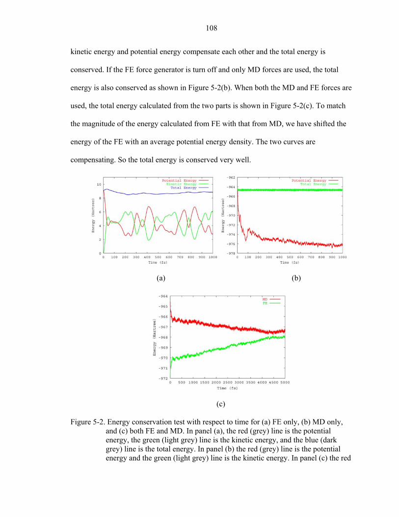
108
kinetic energy and potential energy compensate each other and the total energy is
conserved. If the FE force generator is turn off and only MD forces are used, the total
energy is also conserved as shown in Figure 5-2(b). When both the MD and FE forces are
used, the total energy calculated from the two parts is shown in Figure 5-2(c). To match
the magnitude of the energy calculated from FE with that from MD, we have shifted the
energy of the FE with an average potential energy density. The two curves are
compensating. So the total energy is conserved very well.
(a) (b)
(c)
Figure 5-2. Energy conservation test with respect to time for (a) FE only, (b) MD only, and (c) both FE and MD. In panel (a), the red (grey) line is the potential energy, the green (light grey) line is the kinetic energy, and the blue (dark grey) line is the total energy. In panel (b) the red (grey) line is the potential energy and the green (light grey) line is the kinetic energy. In panel (c) the red

109
(grey) line is the total energy from MD part of the calculation and the green (light grey) line is the total energy from the FE part of the calculation, which has been shifted by an average potential energy to match with MD.
(a)
(b)
(c)
(d)
Figure 5-3. Distributions of force and velocity in the y direction during a pulse propagation test for the MD/FE interface. Panel (a) shows the distribution of force in the y direction at time zero. Two atomic layers in the center on the xz plane have been squeezed. The distribution of velocity in the y direction is shown in panel (b), (c) and (d) at the time instants of 0.1, 0.6 and 1.2 ps, respectively.

110
The main goal of the hybrid FE/MD interface is to let elastic waves propagate from
the CMD region to DFE region. To test if our interface works well, we squeeze two
central layers in the direction in the middle of the CMD region to make a pulse and let
it propagate. As seen in Figure 5-3(a), at time zero, only the two central layers feel the
stress. As the dynamics evolves, we plot the distribution of velocity in the direction in
colors at different instants from Figure 5-3(b) to (d). At the beginning, the pulse is in the
center of the wire. Later on, the pulse is propagated into the whole wire. At ps in
Figure 5-3(b), the pulse reaches the TRN region. At
y
y
t 0.1=
0.24t = ps in Figure 5-3(c), the
pulse arrives at the DFE region. Finally, at t 0.6= ps in Figure 5-3(d), the pulse spreads
all over the nanowire and causes some local distortions.
Figure 5-4. The stress-strain relation for a uniaxial stretch applied in the y direction of the nanowire at speed of 0.035 1ps− .
5.3.2 Stretch Simulation
Figure 5-4 shows the stress-strain relation for a uniaxial stretch applied in the y
direction of the nanowire at the speed of 0.035 1ps− . The nanowire breaks at a strain of
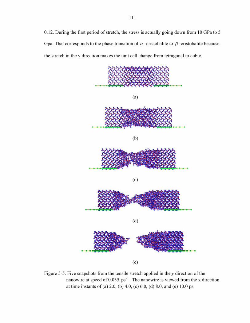
111
0.12. During the first period of stretch, the stress is actually going down from 10 GPa to 5
Gpa. That corresponds to the phase transition of α -cristobalite to β -cristobalite because
the stretch in the y direction makes the unit cell change from tetragonal to cubic.
(a)
(b)
(c)
(d)
(e)
Figure 5-5. Five snapshots from the tensile stretch applied in the y direction of the nanowire at speed of 0.035 1ps− . The nanowire is viewed from the x direction at time instants of (a) 2.0, (b) 4.0, (c) 6.0, (d) 8.0, and (e) 10.0 ps.

112
Under more strain at 2.0t = ps, in Figure 5-5(a), the tetrahedral units around the
surface of the nanowire start to rearrange themselves, to increase the Si-O-Si bond angles
in the direction of the stretch, and to cause local amorphization on the surface. The
neighboring tetrahedra along the x and direction get closer and closer with more
applied strain. When the Si-O bond between neighboring tetrahedra becomes shorter than
that inside the tetrahedron, the bond will break. A fracture tip will be formed if the bond
breaking happens on the nanowire surface or a fracture void will be formed if it happens
inside the nanowire as seen in Figure 5-5(b) at
z
4.0t = ps, when the applied strain is
around 0.12. The fractures propagate and move under further applied strain, and cause
more amorphization as seen in Figure 5-5(c) and (d) at the snapshots of and 8.0
ps. Eventually, the two ends of the nanowire detach around t
6.0t =
10.0= ps in Figure 5-5(e).
The pair correlation functions at t 0.0= and 4.0 ps are shown in Figure 5-6(a) and (b),
respectively. The peaks corresponding to the Si-Si, Si-O and O-O distances at t 4.0= ps
are broadened largely as the nanowire starts to break and becomes amorphous.
(a) (b)
Figure 5-6. Pair correlation functions of the nanowire during the uniaxial stretch simulation. Panel (a) is at 0.0 ps and panel (b) 4.0 ps. In all panels, the solid line is for Si-Si, the short dashed line Si-O, and the dotted line O-O.

CHAPTER 6 SUMMARY AND CONCLUSIONS
In this thesis, the phenomena of surface adsorption and desorption have been
studied by various computational methods. I have presented a detailed microscopic
picture of the interaction between a C60 ML and noble metal (111) surfaces. Large-scale
first-principles DFT calculations have provided complete information of the energetics
and electronic properties, which govern the structure and dynamical processes observed
in experiments. The results are important in understanding the fullerene-metal interfacial
characteristics and properties. Especially, the analysis of changes in surface dipole
moments clarifies the puzzling observation on the work function change of noble metal
(111) surfaces upon the adsorption of a C60 ML. For surface desorption, we have studied
the potential sputtering of a LiF(100) surface stimulated by HCI. The MD formalism is
extended to include the crucial information from electronic excited states, which are
calculated by a high level quantum chemistry method. From the MD simulation, the
experimentally observed sputtering pattern and yield are well reproduced. We find that
the mechanism of potential sputtering has its root in the behaviors of potential energy
functions from electronic excited states. An embedding atom-jellium model has been
formulated into a multiscale simulation scheme to treat only the top metal surface layers
in atomistic pseudopotential and the rest of surface in a jellium model. The calculated
work functions of Al and Cu clean surfaces agree reasonably with the all-atomistic
calculations. We have also studied a multiscale scheme for combining the FE and MD
methods. A gradual coupling of the FE and MD in the interface region is proposed and
113

114
implemented, which shows promising results in the simulation of the breaking of a SiO2
nanowire by tensile stretch.
APPENDIX A TOTAL ENERGY CALCULATION OF SYSTEM WITH PERIODIC BOUNDARY
CONDITIONS
The calculation of total energy per unit cell for a system with periodic boundary
conditions (PBC) is non-trivial. In this appendix, first, a general form of electrostatic
energy in three dimensional PBC is derived following Makov and Payne’s paper
(MP) [204]. Then the interaction among electrons, ions, and the interaction between them
are calculated.
We start with a charge density comprised of electrons and ions,
( ) ( ) ( )i ii
n zρ δ= − + −∑r r r r , (A-1)
where electrons have a continuous distribution ( )n r and ions are sitting at r . This
charge density has a three dimensional periodicity,
i
( ) ( )ρ ρ+ =r rl , (A-2) where are the lattice vectors. The integration of the charge density over , the volume
of the unit cell, can be zero,
l Ω
( ) ( )3 3 0ii
d r d r n zρΩ Ω
= − + =∑∫ ∫r r , (A-3)
which corresponds to the charge neutrality. The electrostatic energy per unit cell can be
written as
( ) ( )312
E d rρ φΩ
= ∫ r r , (A-4)
where
115

116
( ) ( )3d rρ
φΩ
′′=
′− +∑∫r
rr rl l
. (A-5)
is the electrostatic potential generated from the charge density.
The lattice sum for the electrostatic potential in Eq.A-5 is only conditionally
convergent. To make the sum absolutely convergent, we introduce a convergence factor
in the form of Gaussian function,2se . The parameter is a small positive quantity and
approaches zero. In an absolutely convergent sum, we are allowed to exchange the sum
and the integral; therefore, we consider the sum
− l s
( )2 1, ss eχ −=
+∑xx
l
l l, (A-6)
where . Now we introduce the Gamma function identity ′= −x r r
( )
22 1
0
1a ty dt ea
∞ y at− − −=Γ ∫ . (A-7)
With the special case of 1 2a = and ( )1 2 1 πΓ = , and the substitution of y = +x l , the
sum can be rewritten as
( ) ( ) 221 2 1 2
0, sts dt t eχ π
∞ −− +− −= ∑∫ xx ll
le . (A-8)
This integral is singular at the limit 0t = , when 0s = . To isolate this singularity, we split
the integration range into two, 20,η and 2 ,η ∞ . Thus ( ), sχ x is also split into two
parts,
( ) ( ) ( )1 2, , ,s s sχ χ χ= +x x x . (A-9) The second part is reduced to the complementary error function as

117
( ) ( )
( )
22
2
2
1 2 1 22 ,
.
st
s
s dt t e
erfce
ηχ π
η
∞ −− +− −
−
=
+=
+
∑∫
∑
xx
xx
ll
l
l
l
ll
e
(A-10)
The first part can be rearranged into
( ) ( )
( )
( )
2 22
222
222
1 2 1 21 0
1 2 1 2
0
1 2 1 2
0
,
.
st
t tst st s t s
tts t st st s
s dt t e e
dt t e e
dt t e e
η
η
η
χ π
π
π
−− +− −
− + + − +− − +
− + +− +− − +
=
=
=
∑∫
∑∫
∑∫
x
x x
xx
x ll
l
l
l
l
l
(A-11)
In the last line of Eq.A-11, the exchange of sum and integral is used.
The goal is to convert the sum of Gaussian functions in ( )1 , sχ x from real space to
reciprocal space in Eq.A-11. To make notation concise, we introduce and (a t s= + )
)(u t t s= + . The sum can be expressed in reciprocal space as
( ) ( )
( )
2 2
, .
a u a
i
e e
g a e
′− + − +
′
=
=
∑ ∑
∑
x x
G x
GG i
l l
l l (A-12)
In the first line of Eq.A-12 above, we made the substitution of u′ =x x
)
. The coefficient
is the Fourier transform of , which is independent of as shown
below,
( ,g aG ( )2ae ′− +∑ x l
lu

118
( ) ( )
( )
2
2
2
2
2
3
3
3
3
1
3 24
3 2
1,
1
1
1
1 .
k k k
a i
ia
i a
ax iG xk
k
a
g a d x e e
d x e e
e d x e
dx e
eaπ
′− +
i
′−
Ω
′′−′′−
Ω
′′ ′− −
Ω
∞ ′′ ′′− −
−∞=
−
′=Ω
′′=Ω
′′=Ω
′′=Ω
=Ω
∑∫
∑∫
∑ ∫
∏∫
x G x
G x -x
G x
G
G i
i
i
l
l
l
l
l
l
′G x (A-13)
In the second line of Eq.A-13, the change of variable ′′ ′= +x x l is made. In the fourth
line, ∑ is used and the integral is decomposed into each component. In the last
line, the result of a one-dimensional Gaussian integral is used.
ie =G l
l
i N
Putting Eq.A-12 and Eq.A-13 back into Eq.A-11, we get
( ) ( ) ( )2
223 2 41 2
1 0,
ts tit st s t ss dt t t s e e eηπχ
− − − +− + = +Ω∑∫
Gx G
Gx
i+
x. (A-14)
For , the sum in Eq.A-14 is absolutely convergent when 0≠G 0s = ,
( )
22
2
2
421 0 0
42
,
4 1 .
t i
i
s dt t e
e e
η
η
πχ
π
− −
≠≠
−
≠
= Ω
=Ω
∑ ∫
∑
GG x
GG 0
GG x
G 0
x
G
i
i
e (A-15)
However, the term is singular when 0=G 0s = . Again we make the substitution of
( )u t t s= + , so that ( )2dt du t s s= + , to obtain
( ) ( )( )2 2 21 2
1 0 0,
s s us du us
η ηeπχ
+ −− = Ω ∫x
G=x . (A-16)
Expand the exponential and carry out the integration of the first few terms to get

119
( ) ( ) ( )( )
( )
( ) ( )
( )
2 21 2 2 2
1 0 0
2 3
3 22 2
22
2
2
2
2 22
, 1
2 23
2 212 3
2 23
2 2 2 .3
ss du u s u
s
ss s s
s O s O ss
s
s
η η
1
O sπχ
π η ηη η
π πη
π π πη
π π πη
+ − = − + Ω − Ω + +
= − + − + Ω Ω
− −Ω Ω Ω
′ ′= − − + −Ω Ω Ω
∫G=x x
x
x
x
r r r ri
(A-17)
In the third line of Eq.A-17 above, the expansion of denominators is used to keep terms
other than O s . ( )
Now put all things together into Eq.A-5, take the limit of 0s = , and notice that
when is multiplied by ( , sχ x ) ( )ρ ′r and integrated over a charge neutral cell, the first
three terms become zero. This means that the singularity of the potential at , when
, simply cancels out for charge neutral cell. Thus we get
0=G
0s =
( ) ( ) ( ) ( )3 2, 23
d r πφ ρ χΩ
2′ ′ ′ ′= − Ω ∫r r r r r i ′− r r , (A-18)
and
( ) ( ) (
2
242
0
4 1, ierfce eηη πχ
− ′−
≠
′− +′ = +
′− + Ω∑ ∑G
G r r
G
r rr r
r r Gl
ll
i ) . (A-19)
In calculating the energy, we again use the condition of charge neutrality. The first term
of the following equation is zero,
( ) ( ) ( ) ( )2
3 3 2 31 2 222 3 3
d r d r d rπ πρ ρ ρΩ Ω Ω
′ ′ ′ ′− − = Ω Ω ∫ ∫ ∫r r r r r ri r . (A-20)
So we obtain the energy
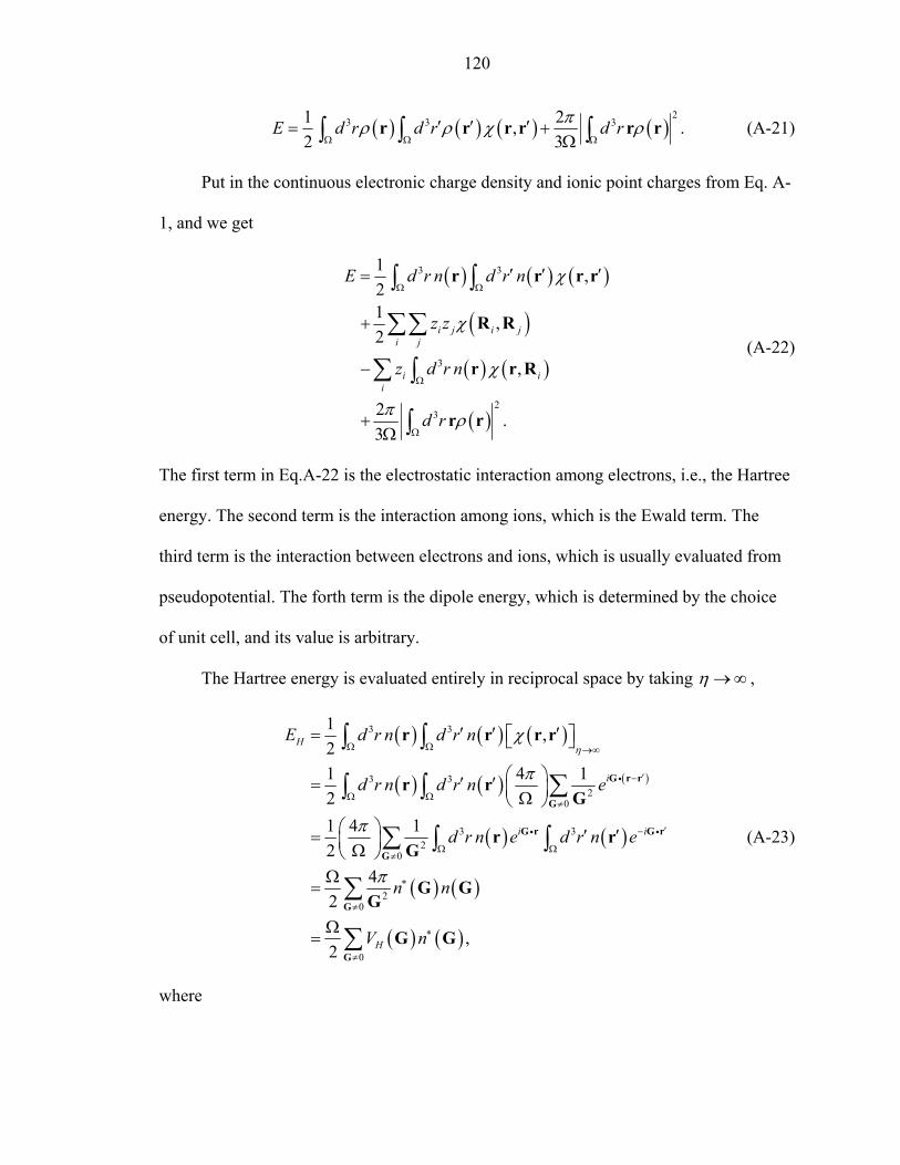
120
( ) ( ) ( ) ( )2
3 3 31 2,2 3
E d r d r d rπρ ρ χ ρΩ Ω Ω
′ ′ ′= +Ω∫ ∫ ∫r r r r r r . (A-21)
Put in the continuous electronic charge density and ionic point charges from Eq. A-
1, and we get
( ) ( ) ( )
( )
( ) ( )
( )
3 3
3
23
1 ,21 ,2
,
2 .3
i j i ji j
i ii
E d r n d r n
z z
z d r n
d r
χ
χ
χ
π ρ
Ω Ω
Ω
Ω
′ ′ ′=
+
−
+Ω
∫ ∫
∑∑
∑ ∫
∫
r r
R R
r r R
r r
r r
(A-22)
The first term in Eq.A-22 is the electrostatic interaction among electrons, i.e., the Hartree
energy. The second term is the interaction among ions, which is the Ewald term. The
third term is the interaction between electrons and ions, which is usually evaluated from
pseudopotential. The forth term is the dipole energy, which is determined by the choice
of unit cell, and its value is arbitrary.
The Hartree energy is evaluated entirely in reciprocal space by taking η →∞ ,
( ) ( ) ( )
( ) ( ) ( )
( ) ( )
( ) ( )
( ) ( )
3 3
3 32
0
3 32
0
20
0
1 ,21 4 121 4 12
42
,2
H
i
i
H
E d r n d r n
d r n d r n e
d r n e d r n e
n n
V n
ηχ
π
π
π
Ω Ω →∞
′−
Ω Ω≠
′−
Ω Ω≠
∗
≠
∗
≠
′ ′ ′ =
′ ′= Ω ′ ′= Ω
Ω=
Ω=
∫ ∫
∑∫ ∫
∑ ∫ ∫
∑
∑
G r r
G
G r G r
G
G
G
r r r r
r rG
r rG
G GG
G G
i
i i i (A-23)
where

121
( ) ( )2
4HV nπ
=G GG
. (A-24)
is defined as the Hartre potential.
The ion-ion interaction energy is
( )
( )
( )
( ) ( )
2
2
2
0
42
2 2
00
1 1 1, lim2 2
1 4 12
12
1 1 lim .2 2
ion ion i j i j ii j i
ii j
i j
i ji j
i j i i j
i ii i
E z z z
z z e e
erfcz z
erfc erfcz z
η
χ
π
η
η η
− →
− ′−
≠
≠
→≠
= −
= Ω
− ++
− +
+ +
∑∑ ∑
∑∑ ∑
∑∑ ∑
∑ ∑ ∑
GG r r
G 0
R R
G
R R
R R
i
l
l
ll
l
l
l
l ll l
1−l
(A-25)
The last term in the first line is the unphysical interaction between a point charge with
itself inside the central unit cell 0=l , which needs to be subtracted. After writing out all
the terms explicitly in the second line, the first term is the summation in reciprocal space.
The second term is the interaction between different ions in real space. The third term is
the interaction between an ion with its image charge in the neighboring unit cells. The
last term combines the term from the error function with 0=l for and the
unphysical term. Both of them diverge individually, but the combined term is finite
because
i = j
( ) 2
00 0
1 1 2lim lim yerfcdy e
ηη 2ηπ π
−
→ →
− = − = −
∫l
l l
ll l l
. (A-26)
So the ion-ion interaction energy is
122
( )
( )
2
242
2
1 4 12
1 ,2
iion ion i j
i j
i ji j i
i j ii j
E z z e e
erfcz z z
ηπ
η ηπ
− ′−
−≠
∗
= Ω
− ++ −
− +
∑∑ ∑
∑∑ ∑ ∑
GG r r
G 0 G
R R
R R
i
l
l
l
(A-27)
where the star means for 0≠l i j= .
The interaction between electrons and ions is
( ) ( ) ( )
( ) ( )
( ) ( )
3 3
3 32
0
20
,
4 1
4 ,
el ion i ii
i ii i
i
E d r n d r z
d r n e d r z e
S n
η
δ χ
π δ
π
− Ω Ω→∞
′−
Ω Ω≠
∗
≠
′ ′ ′ = − −
′ ′= − −Ω
= −Ω
∑∫ ∫
∑ ∑∫ ∫
∑
G r G r
G
G
r r R r r
r rG
G GG
i iR (A-28)
where
( ) iii
i
zS − = Ω ∑ G RG ie (A-29)
defines the structure factor. Eq.A-28 has no practical use unless the ions reduce to nuclei
in an all-electron calculation. The equation oversimplifies the interaction between
extended ions and valence electrons.
Usually, the interaction felt by valence electrons from ions is modeled by a
pseudopotential V . We follow the notation from Ihm et al.’s paper (IZC) [205] and
write
( ),ps l r
( ) ( ) ( )3,
, ,
ˆps i ps l l i
i lE d r V Pµ
µ
ψ ψ∗= −∑ ∫ r r R r , (A-30)
where the projection operator is
,
ll m
P lm l= m∑ . (A-31)
123
The subscript i stands for both state and k-point, µ stands for ions, and and stands
for angular and magnetic momentum number. With a plane wave expansion,
l m
( ) ( ), ,
1 ii iC eψ +
+=Ω∑ k G r
k k GG
r i , (A-32)
and with a change of variable ( )µ− →r R r , Eq.A-30 can be cast into the reciprocal
space
( ) ( ) ( ) ( )
( )
3, , ,
, , ,
, , , , ,, , ,
ˆ
.
i iips i i ps l l
i l
i i ps li l
E C C e d r e V P e
C C S V
µ
µ
′′ − + + − −∗ ′+ +
′+ +
∗′ ′+ + + +
′+ +
= Ω
′= Ω −
∑ ∑ ∫
∑
k G r k G rG G Rk G k G
k G k G
k G k G k G k Gk G k G
r
G G
i ii
(A-33)
In Eq.A-33 above, the structure factor is
( ) ( )1 iS e µ
µ
′− − ′− = Ω ∑ G G RG G i , (A-34)
and the Fourier transform of the pseudopotential is
( ) ( ) ( )
( ) ( ) ( ) ( ) ( )
3, , , ,
2,
ˆ
4 2 1 cos
i ips l ps l l
ps l l l l
V d r e V P e
l dr r V r j r j r P ,π γ
− + + ′+ + =
′= + + +
∫∫
k G r k G rk G k G r
k G k G
i i
(A-35)
where
( ) ( )cosγ′+ +
=′+ +
k G k Gk G k G
i. (A-36)
We have used the spherical Bessel functions and the Legendre polynomials . We
also have used
lj lP
( ) ( ) ( ) ( ) ( )0
2 1 coslil l
le i l j r P
r
∞+
=
+= − + + + ∑k G r k G r
k Gk G
i i . (A-37)
For the local part of pseudopotential, it is straightforward to write
124
( ) ( ) ( )
( ) ( )
( ) ( ) ( )
( ) ( ) ( )
3
,
3
3
.
ps i ps ii
ps
ips
ps
E d r V
d rV n
d r V e n
S V n
µ
µµ
µµ
µ
ψ ψ∗
−
∗
= −
= −
=
=
∑∫
∑∫
∑ ∑∫
∑
G r R
G
G
r r R
r R r
G r
G G G
i
r
(A-38)
Notice that the diverging components of the electrostatic potential in Eq.A-23,
Eq.A-25, and Eq.A-28 cancel out for a charge neutral cell is the result of purely
Coulombic interaction. Since we replace the Coulombic interaction between ions and
electrons by a smoother pseudopotential, an offset should be introduced. This is the
0=G
Zα
term in Ihm et al.’s paper [205], which is just the difference between the Coulomb
interaction and the pseudopotential at 0=G .
The band structure energies and Hellmann-Feyman theorem can be found in IZC
paper. The treatment of aperiodic or charged system is in MP paper.

APPENDIX B REVIEW OF DEVELOPMENT IN FIRST-PRINCIPLES PSEUDOPOTENTIAL
B.1 Norm-Conserving Pseudopotential
The idea of a pseudopotential is to eliminate the chemically inert core states within
the frozen core approximation and concentrate on the chemically active valence states.
The true potential of the valence states felt from the core states and nuclei is replaced by
a much smoother effective potential. This pseudopotential results in pseudo wave
functions that are the same as the true valence wave functions outside the small core
region, but avoid the radial nodes that keep the true valence and core wave function
orthogonal. There are two classes of pseudopotential seen in literature. Empirical
pseudopotentials [206] are fitted with a few parameters to reproduce the experimental
electronic structure. First-principles pseudopotentials date back to Herring’s invention of
the orthogonalized plane wave (OPW) method [207]. Later, Phillips et al. [208] and
Antoncik [209] reformulated the OPW method, replaced the orthogonality condition by
an effective potential, and established the first-principles pseudopotential method.
Modern first-principles pseudopotential study starts from the works of Hamann, Schlüter,
and Chiang (HSC) [210] and Zunger and Cohen [211, 212]. There were improvements by
Kerker [213], Troullier and Martins [214, 215], and Rappe et al. [216] Recently, major
improvements were made by Vanderbilt [50] and Blöch [217-219] to make the ultrasoft
pseudopotential and the projector augmentation method (PAW), respectively.
The construction of first-principles pseudopotentials starts with the solution of the
all-electron Schrödinger equation for an isolated atom in a certain reference configuration
125

126
with DFT formulism. After the angular part is separated, the scalar-relativistic radial
Schrödinger equation is
( ) ( )
( ) ( ) ( ) ( )2 2
2 2
11 1 02 2 l l
dV r l ld dr V r uM r dr M r dr dr r r
α ε +
− − + + − = r , (B-1)
where
( ) ( )( )2
12 lM r Vα ε= + − r , (B-2)
( ) [ ] [;H xcZV r V n r V n rr
= − + + ]; , (B-3)
and α is the fine structure constant. The radial wave function ( )nlu r is defined as usual,
( ) ( ) ( ) ( ) ( ), ,nlnlm nl lm lm
u rr R r Y Y
rφ θ ϕ θ ϕ= = . (B-4)
Since the angular wave function does not change in pseudoization, we mean pseudo wave
function as for the pseudo radial wave function ( )l ru . We use the convention that the
symbols with tilde are for pseudo quantities. We also drop the quantum number n
because it does not affect the process of pseudoization.
There are several conditions that the pseudo wave function must meet with respect
to the true wave function.
(i) The pseudo wave function must have the same eigenvalue as the true wave function
for the chosen electronic configuration (usually the atomic ground state),
l lε ε= . (B-5) (ii) The pseudo wave function must be nodeless and be identical to the true wave function
beyond a chosen core radius,

127
( ) ( )l lu r u r for r rcl= > . (B-6) (iii) The charge enclosed within the core radius for the pseudo and true wave function
must be equal,
. (B-7) ( ) ( )2 2
0 0
cl clr r
l lu r dr u r dr=∫ ∫ (iv) Both the first and second derivatives of the pseudo wave function at the core radius
must be matched to the values of the true wave functions.
( ) ( )
( ) ( )2 2
2 2 .
cl cl
cl cl
l r r l r r
l r r l r r
d du r u rdr drd du r u rdr dr
= =
= =
=
= (B-8)
From these conditions for pseudo wave function, requirements on the pseudopotential can
be derived. From condition (ii) and (iii), the norm for the pseudo and true wave function
are the same for any radius beyond the core radius as
( ) ( )2 2
0 0
r r
l lu r dr u r dr for r r′ ′
′ cl= ≥∫ ∫ . (B-9)
From Gauss theorem, this means that the electrostatic potential outside of the core radius
is reproduced. With the identity [220, 221]
2 2
0
1 ln2
rll l
r
ud du ud dr rε
′
′
− =
∫ dr , (B-10)
it can be derived that
( ) ( )ln lnl ld du r u r for r rdr dr cl= ≥ . (B-11)
This means the scattering property of the pseudopotential is the same as the true
potential, which ensures the transferability of the pseudopotential. Practically, the
128
conditions (i) through (iv) are used to determine the parameters for the pseudo wave
function once its form is decided.
The pseudopotential is then obtained by inversion of the non-relativistic radial
Schrödinger equation with pseudo wave function,
( ) ( ) ( )2
2 2
11 02 2
scrl l l
l ld V r u rdr r
ε +− + + − =
. (B-12)
The resulting pseudopotential is
( ) ( )( ) ( )
2
2 2
1 12 2
scrl l l
l
l l dV r u rr u r dr
ε+
= − + . (B-13)
It is labeled as a screened pseudopotential because it includes the screening effect from
other valence states, in addition to the core states.
There are a lot of recipes to generate pseudo wave functions and pseudopotentials
in the literature. HSC used a scheme as following [210, 222]: After the all-electron
scalar-relativistic radial Schrödinger equation is solved, the true potential is modified,
which is then put into a non-relativistic radial Schrödinger equation to get an intermediate
wave function. The intermediate wave function will then be modified to the pseudo wave
function by meeting all the conditions. Finally the non-relativistic radial Schrödinger
equation is inverted with the pseudo wave function to get the screened pseudopotential.
Kerker [213] was the first to use the recipe that modifies the true wave function
directly as the starting point to get the pseudo wave function. Then the pseudo wave
function was used to invert the non-relativistic radial Schrödinger equation to get the
screened pseudopotential. This scheme is more popular since the pseudopotential is
derived in an analytically less complicated way and with no need to solve Schrödinger
equation twice. The form of pseudo wave function is
129
( )( )
( )1,l c
l p rlcl
u r for r ru r
r e for r r+
≥= ≤
l (B-14)
where
( )4
02
ii
ip r c c r
=
= +∑ . (B-15)
In the polynomial expansion, the coefficient of is omitted to avoid the singularity of
the screened pseudopotential at the origin
1c
0r = . The screened pseudopotential is
obtained as
( )( )
( ) ( ) ( ) 21
2 2
AEl cl
scrl
l c
V r for r rV r p r p rp rl
lfor r rr
ε
≥
= ′′ ′ +′+ + + ≤
. (B-16)
Troullier and Martins [214, 215] generalized Kerker’s recipe by increasing the order of
the polynomial to with only the even terms. The additional coefficients give the
freedom to investigate the smoothness properties of the pseudopotential.
12n =
In stead of using polynomial and exponential functions, Rappe and Rabe et
al. [216] used a linear combination of spherical Bessel functions as the pseudo wave
function inside the core region. They also proposed a way to minimize the kinetic energy
contained in the Fourier components of beyond a certain cutoff of wave vector. lu
The pseudopotential that is directly used in solid state calculations is actually an
ionic pseudopotential. The ionic pseudopotential is obtained by subtracting the
contribution due to valence electrons from the screened pseudopotential,
( ) ( ) [ ] [ ]; ;ion scrl l H xcV r V r V n r V n rυ υ= − − , (B-17)

130
where nυ is the valence electron density. The total ionic pseudopotential can be written
out as,
( ) ( ) ( ) ( ) ( )ion ionlm l lm
lmV Y V r r r Yδ ∗
′′= Ω − Ω∑ rr r . (B-18)
It is in a semi-local form because the radial part is local, but the angular part is nonlocal.
When the matrix element is evaluated for the ionic pseudopotential as,
( ) ( ) ( ) ( ) ( ) (3 3
,
ion ionn n n lm l lm n
l mV d r d r Y V r r r Yψ ψ ψ δ ψ∗ ∗
′ ′ ′ )′ ′ ′= Ω −∑∫ ∫ r rr rΩ , (B-19)
where stands for the state, k-point and spin index, the integral of n
( ) ( ) ( ) ( )2 cosionl l l ldr r j r V r j r P γ + +′+ +∫ k G.k G'k G k G (B-20)
must be calculated by ( )1 2MN N + times, where M is the number of k-points and
is the number of plane wave vectors. Kleinmen and Bylander (KB) [223] proposed a fully
separable form for the ionic pseudopotential as
N
( ) ( ) ( ) ( ),
ion ionl l l lion ion
loc lm lmionl m l l l
V u u VV V r Y Y
u V uδ δ
δ∗
′= + Ω Ω∑ r rr , (B-21)
where
( ) ( ) ( )ion ion ionl l locV r V r V rδ = − , (B-22)
( ) ( )ion ion
l l l lV u V r u rδ δ= , (B-23) and V is usually chosen to be V . Now the matrix element is evaluated as following, ion
loc max
ionl
( ) ( ) ( )
( ) ( )( ) ( ) ( ) ( ) ( ) ( ) ( ) ( )
3 323
,
3 3
1
.
ion ionn n n loc n ion
l m l l
ion ionn lm l l l l lm n
V d r d r V rd r V r u r
d r Y V r u r d r V r u r Y
ψ ψ ψ ψδ
ψ δ δ ψ
∗′ ′
∗ ∗′ ′
′= +
′ ′ ′× Ω Ω
∑∫ ∫∫
∫ ∫r r
r r
r r′
(B-24)

131
The number of operations is reduced to MN times. When using the KB fully separable
form, spurious eigenstate or “ghost states” must be eliminated by close examination.
B.2 Ultrasoft Pseudopotential and PAW
The norm-conserving pseudopotential is very successful in describing the
semiconductor elements and the elements nearby, such as, Si and Al. But it needs a very
large kinetic energy cutoff to describe the first row elements, transition and noble metal
elements, which have localized valence states. The difficulty comes from the fact that the
cutoff core radius can not be increased too far away from where the maximal of the true
radial wave function occurs. Otherwise, the norm-conserving condition can not be
satisfied. This problem is solved in the ultrasoft pseudopotential formalism as proposed
by Vanderbilt [50] and independently by Blöchl [217]. Another improvement is made by
including more reference energies to increase the transferability of the
pseudopotential [50, 217, 224].
We follow the presentation of Vanderbilt’s paper [50]. Start with the all-electron
Schrödinger equation for an isolated atom,
( ) 0AE i iT V ε φ+ − = , (B-25) where i . Now a pseudo wave function ( ilmε= ) iφ is constructed satisfying the
conditions. By choosing a local pseudopotential V , we can define, loc
( )i loc iT V iχ ε φ= − + − , (B-26) where iχ is local and short ranged because beyond , Vcr loc AEV= and i iφ φ= . The
nonlocal pseudopotential operator in the KB form is well-defined as,
132
i iNL
i i
Vχ χχ φ
= . (B-27)
Now the eigenvalue problem is for the pseudo wave function and pseudo Hamiltonian,
( ) ( )
( ) ( )0.
i i iloc NL i i loc i i
i i
loc i i loc i i
T V V T V
T V T V
χ χ φε φ ε φ
χ φ
ε φ
+ + − = + − +
= + − − + −
=
ε φ (B-28)
Furthermore, we can introduce iβ as,
( )1i jij
jBβ χ−=∑ , (B-29)
where
ij i jB φ χ= . (B-30) It is shown below that iβ is the dual of iφ because
( ) ( )1 1s i s jji ji
j jB B sj siBφ β φ χ− −= = δ=∑ ∑ . (B-31)
Now the nonlocal part of the pseudopotential is simplified to be
,
NL ij i ji j
V B β β=∑ . (B-32)
Notice that iβ is equivalent to the core orbital in the original Phillips-Kleinman
pseudopotential [208] and the projection operator ip , which we will show later in PAW
method [218, 219].
The norm-conserving condition can be generalized to be
0ijQ = , (B-33)
133
where
c c
ij i j i jr rQ φ φ φ φ= − (B-34)
is a Hermitian operator. It can be shown that the matrix ijB , and therefore V are
Hermitian when . We can write out
NL
0ijQ = ijB in terms of the radial wave function
( )iu r r associated with as ( )iφ r
( ) ( ) ( ) ( )2
2 20
112 2
cr
ij i j loc j
l ldB dr u r V r u rdr r
ε∗ += + − −
∫ . (B-35)
After integration by parts, we get
( ) ( ) ( ) ( ) ( )12c
ij ji j i i j i c j c i c j crB B u r u r u r u rε ε φ φ∗ ∗ ′ ′∗ − = − + − . (B-36)
Also from the all-electron Schrödinger equation, we have
( ) ( ) ( ) ( ) ( )102c
j i i j i c j c i c j cru r u r u r u rε ε φ φ ∗ ∗′ ′ = − + − . (B-37)
Subtracting Eq.B-37 from Eq.B-36, we get
( )ij ji i j ijB B Qε ε∗− = − , (B-38) because the true and pseudo wave function and their derivatives match at . So when
,
cr
0ijQ = ijB and V are both Hermitian. NL
The constraint of is not necessary if one is willing to deal with a
generalized eigenvalue problem in which an overlap operator
0ijQ =
,
1 ij i ji j
S Q β β= +∑ (B-39)
appears. It has the following property,

134
,
.
c c
c
c
i j i j st i s tr rs t
i j ijr
i j r
S Q
Q
jφ φ φ φ φ β β
φ φ
φ φ
= +
= +
=
φ∑
(B-40)
Now the nonlocal pseudopotential operator can be defined as
,
NL ij i ji j
V D β β=∑ , (B-41)
where
ij ij j ijD B Qε= + . (B-42) The operators ijB and are given in Eq.B-30 and Eq.B-34 respectively. Although ijQ ijB is
not Hermitian, and are Hermitian because ijQ ijD
( ) ( ) 0ij ji ij ji j ij i ji i j ij j i ijD D B B Q Q Q Qε ε ε ε ε ε∗ ∗ ∗− = − + − = − + − = . (B-43) The generalized eigenvalue problem follows as
( ) ( )
( )
( )
( ) ( )
( )
, ,
,
1
,
0.
i i loc NL i i
loc i st s t t st s t is t s t
i i st s t is t
loc i i si ss
loc i i si jjss j
loc i i i
H S T V V S
T V B Q
Q
T V B
T V B B
T V
ε φ ε φ
φ β β ε β β φ
ε ε β β φ
ε φ β
ε φ χ
ε φ χ
−
− = + + −
= + + +
− +
= + − +
= + − +
= + − +
=
∑ ∑
∑
∑
∑
(B-44)
The cost of solving the generalized eigenvalue problem does not increase comparing to
the original eigenvalue problem, since the most time consuming procedure is the
multiplication of H Sε− with a trial vector φ .

135
The relaxation of the constraint of Q 0ij = makes it possible to choose the cutoff
radius to be well beyond the maximum of the true wave function, because the only
constraint is the matching of ( )i rφ and ( )i rφ at the cutoff radius. Since a generalized
eigenvalue problem must be solved in the target solid-state calculation, the deficit of the
valence charge in the core region associated with a pseudo wave function needs to be
restored. At first, the solution to the generalized eigenvalue problem in a solid-state
calculation, nψ k should be normalized as
n nS nnψ ψ δ′ ′=k k , (B-45) where stands for a band index, a k-point and a spin index. The valence charge density
is
n
( ) ( ) ( ), ,
v n n ij jin i j
n ψ ψ ρ∗= + Q∑ ∑k kk
r r r , (B-46)
where
,
ij i n n jn
ρ β ψ ψ β=∑ k kk
. (B-47)
The variational electronic total energy is
[ ] [ ], ,
ion ionn loc ij i j n H v xc v
n i jE T V D E n E nψ β β ψ
= + + + +
∑ ∑k k
kcn+ , (B-48)
where V and are the unscreened parts of V and . Applying a variation to the
electronic total energy with the constraint in Eq.B-45, we get the secular equation as
ionloc
ionijD loc ijD
( ) 0loc NL n nT V V Sε ψ+ + − =k k , (B-49) where
, (B-50) ionloc loc HxcV V V= +

136
, (B-51) ion Hxcij ij ijD D D= +
and
( ) [ ] ( ) [ ] ( )v v cn n nHxc H xcV V V += +r r r , (B-52)
( ) ( )3Hxc
ij Hxc ijD d rV Q= ∫ r r . (B-53) The dependence of on ijD nυ through HxcV means that the pseudopotential must be
updated as part of the self-consistent procedure.
In the pseudopotential method, the key concept is the replacement of true atomic
wave function with pseudo atomic wave function for chemically active valence states.
The wave function we then get for the target system is also “pseudo”, in contrast to the
true wave function of the system. But these pseudo wave functions totally determine the
chemical properties that we are interested in. This concept of pseudization of wave
functions is further generalized in the PAW method by Blöchl [218, 219]. In general,
there is a linear transformation ℑ between the true wave function and the pseudo wave
function or the so called auxiliary wave function as
n nψ ψ= ℑ , (B-54) where, as usual, stands for a band index, a k-point and a spin index. The difference
between the true and the auxiliary wave function is the nodal structure of the former and
the smoothness of the later in the atomic core region.
n
The transformation operator ℑ must be able to modify the smooth auxiliary wave
function to the true wave function in each atomic region. So it is straightforward to write
it as an identity operator plus contributions from each atomic site as RS
1 RR
Sℑ = +∑ , (B-55)

137
where R denotes all the atomic sites. To find the local contribution, we start with the
transformation between the true atomic wave function iφ and the pseudo atomic wave
function iφ for the isolated atom on site . They are also called the partial wave
function and the auxiliary wave function,
i
( )1i R iS for iφ φ R= + ∈ . (B-56) Equivalently,
R i i iS φ φ φ= − , (B-57) which defines the local contribution to the transformation operator. As usual, we
require that the partial wave
RS
iφ and its auxiliary counter part iφ are the same beyond a
certain cutoff radius.
To be able to apply the transformation to an arbitrary auxiliary wave function, we
need to have the following expansion
( ) ( ) ,n i i n Ri R
c Rp for rψ φ ψ∈
= − <∑r r r R , (B-58)
where ip is defined as the projector function, which is a dual to iφ ,
,1 ,
i j ij
i i R c Ri
p and
.p for i j R and r
φ δ
φ
=
= ∈ − <∑ r R (B-59)
Here ip is similar to iβ in ultrasoft pseudopotential method. The way to construct
ip is discussed in detail in Blöchl’s paper [218]. The local transformation operator can
be expressed as
138
( )R n R i i n i i i ni R i R
S S p pψ φ ψ φ φ ψ∈ ∈
= = −∑ ∑ . (B-60)
So the transformation operator ℑ is
( )1 1R i iR i
S pφ φℑ = + = + − i∑ ∑ , (B-61)
where i goes over all the atomic sites and the partial waves within.
Now applying the transformation operator to an arbitrary auxiliary wave function,
we get
( ) ( )1 1, ,n n i i i n n n R n R
i Rpψ ψ φ φ ψ ψ ψ ψ= + − = + −∑ ∑ , (B-62)
where
1,n R i i n
i Rpψ φ ψ
∈
=∑ , (B-63)
1
,n R i i ni R
pψ φ ψ∈
=∑ . (B-64)
The expectation value of an operator is A
1
cNc c
n n n i in i
A f A Aψ ψ φ=
= +∑ ∑ φ . (B-65)
It can be written out as
( ) ( )
( )( )
1 1 1 1, , , ,
1 1 1 1, , , ,
1 1 1 1 1 1, , , , , ,
1 1 1 1, , , , ,
n n n n R n R n n R n RR R
n n n R n R n R n RR
n R n R n n R n n R n R n RR
n R n R n R n RR R
A A
A A A
A A
A
ψ ψ ψ ψ ψ ψ ψ ψ
ψ ψ ψ ψ ψ ψ
ψ ψ ψ ψ ψ ψ ψ ψ
ψ ψ ψ ψ
′ ′′
′ ′′≠
= + − + −
= + −
+ − − + − −
+ − −
∑ ∑
∑
∑
∑
(B-66)

139
where the third line in Eq.B-66 is zero because the function 1,n R n R
1,ψ ψ− is zero beyond a
certain augmentation region and the function 1,n n Rψ ψ− is zero inside that same
augmentation region. So the product of them is zero. Similarly, the forth line in Eq.B-66
is zero because the functions 1,n R n R
1,ψ ψ− from different atomic sites never overlap. So we
have
( )
, ,
1 1 1 1, , , ,
1
1
, ,,
c
c
c R c R
Nc c
n n n n R n R n R n R i in R i
Nc c
n n n i in i
N Nc c c c
ij j i i i ij j i i iR i j R i R R i j R i R
A f A A A A
f A A
D A A D A A
ψ ψ ψ ψ ψ ψ φ φ
ψ ψ φ φ
φ φ φ φ φ φ φ φ
=
=
∈ ∈ ∈ ∈
= + − +
= +
+ + − +
∑ ∑ ∑
∑ ∑
∑ ∑ ∑ ∑ ∑ ∑
(B-67) where
ij n n j i n i n n n jn n
f p p p f pψ ψ ψ ψΘ = =∑ ∑ , (B-68)
which is defined as the occupancies of each augmentation channel ( ) . ,i j
Here we introduce the auxiliary core wave functions ciφ , which is identical to the
tails of the true core wave functions ciφ outside the augmentation region. This allows us
to include the tails of core wave functions in the plane wave expansion, which is better
than the ultrasoft pseudopotential case. So every operator’s expectation value can be
written as three parts. The first part is from the auxiliary wave functions of the whole
system in the expansion of plane waves. What has been missed is the part from the core
region, which is achieved by two parts. The second part from the true onsite partial wave
expansion of each atom is added. Then the third part from the auxiliary onsite partial

140
wave expansion, which is only nonzero outside the atomic region and must be subtracted.
For example the electron density is
( ) ( ) ( ) ( )( )1 1R R
Rn n n n= + −∑r r r r , (B-69)
where
( ) ( ) ( )n n n cn
n f ψ ψ∗ n= +∑r r r , (B-70)
( ) ( ) ( )1
,,
R ij j ii j R
n φ φ∗
∈
= Θ + c Rn∑r r r , (B-71)
( ) ( ) ( )1
,,
R ij j ii j R
n φ φ∗
∈
= Θ + c Rn∑r r r , (B-72)
and is the core density of the atom and is the auxiliary core density that is
identical with outside the atomic region and a smooth continuation inside. Another
example is the total energy
,c Rn ,c Rn
,c Rn
[ ]( ) ( )1 1,n i R RR
E R E E Eψ = + −∑ , (B-73)
and
( ) ( ) ( ) ( )
( ) [ ]( ) ( ) ( )
2 3 3
3 3
1 12 2
,
n nn
xc
n Z n ZE d r d r
d r n , n d r n
ψ ψ
ε υ
′ ′ + + ′= − ∇ +′
+ +
∑ ∫ ∫
∫ ∫
r r r rr - r
r r r r
(B-74)
( ) ( ) ( ) ( )
( ) ( )
,1 2 2
,
1 13 3 3 1 1
1 12 2
1 ,2
c RNc c
R ij j i i ii j R i R
xc
E
n Z n Zd r d r d r n , n
φ φ φ φ
ε
∈ ∈
= Θ − ∇ + − ∇
′ ′ + + ′ + + ′
∑ ∑
∫ ∫ ∫r r r r
r rr - r
(B-75)
( ) ( ) ( ) ( )
( ) ( ) ( ) ( )
1 11 2 3 3
,
3 1 1 3 1
1 12 2
,
R ij j ii j R
xc
n Z n ZE d r d r
d r n , n d r n
φ φ
ε υ
∈
′ ′ + + ′= Θ − ∇ +′
+ +
∑ ∫ ∫
∫ ∫
r r r rr - r
r r r r
(B-76)

141
where is defined as the sum of the delta functions on the nuclear sites and ( )Z r ( )Z r is
defined as a sum of angular-momentum-dependent Gaussian functions. It is constructed
such that the augmentation charge density ( ) ( ) ( ) (1 1R R R Rn Z n Z+ − −r r r )r has zero
electrostatic multipole moments outside the atomic region. This achieves the result that
the electrostatic interaction of the one center parts between different sites vanishes.
The matrix element of a general operator with the auxiliary wave functions may be
slowly converging in the plane wave expansion. An example is the singular electrostatic
potential of a nucleus. This problem can be can be solved as following: If an operator B is
purely localized within an atomic region, we can use the identity between the auxiliary
wave function and its own partial wave expansion
1 1 0n n n nB Bψ ψ ψ ψ− = . (B-77) This is only exact for a complete set of projectors. This is why we introduce the potential
( )υ r in the expressions of and to achieve their convergence individually. The
potential
E 1RE
( )υ r must be localized within the atomic region as
,
0n n i i j j nn i j
f p pψ υ φ υ φ ψ
− =
∑ ∑
1
. (B-78)
Finally, the ultrasoft pseudopotential method can be derived as an approximation
from the PAW method. The augmentation part of energy 1E E E∆ = −
ij
is a functional of
the one center occupancies of each augmentation channel Θ . In the expansion of E∆
with respect to ijΘ , if we truncate the expansion after the linear term, the ultrasoft
pseudopotential is recovered as follows,

142
( ) ( ) ( ) ( 2
,
at at atij ij ij ij ij ij
i j ij
EE E O )∂∆∆ Θ = ∆ Θ + Θ −Θ + Θ −Θ
∂Θ∑ . (B-79)
The linear term is the energy related to the nonlocal pseudopotential.

LIST OF REFERENCES
[1] M. P. Allen and D. J. Tildesley, Computer Simulations of Liquids (Clarendon Press,
Oxford, United Kingdom, 1987).
[2] A. Szabo and N. S. Ostlund, Modern Quantum Chemistry: Introduction to Advanced Electronic Structure Theory (Dover Publications, New York, 1996).
[3] R. M. Dreizler and E. K. U. Gross, Density Functional Theory (Springer-Verlag, Berlin, Germany, 1990).
[4] R. G. Parr and W. T. Yang, Density-Functional Theory of Atoms and Molecules (Oxford University Press, Oxford, UK, 1989).
[5] P. Hohenberg and W. Kohn, Physical Review B 136, B864 (1964).
[6] W. Kohn and L. J. Sham, Physical Review 140, 1133 (1965).
[7] H. W. Kroto, J. R. Heath, S. C. Obrien, R. F. Curl and R. E. Smalley, Nature 318, 162 (1985).
[8] T. Sakurai, X. D. Wang, Q. K. Xue, Y. Hasegawa, T. Hashizume and H. Shinohara, Progress in Surface Science 51, 263 (1996).
[9] K. D. Tsuei, J. Y. Yuh, C. T. Tzeng, R. Y. Chu, S. C. Chung and K. L. Tsang, Physical Review B 56, 15412 (1997).
[10] C. T. Tzeng, W. S. Lo, J. Y. Yuh, R. Y. Chu and K. D. Tsuei, Physical Review B 61, 2263 (2000).
[11] D. Purdie, H. Bernhoff and B. Reihl, Surface Science 364, 279 (1996).
[12] A. J. Maxwell, P. A. Bruhwiler, D. Arvanitis, J. Hasselstrom, M. K. J. Johansson and N. Martensson, Physical Review B 57, 7312 (1998).
[13] E. I. Altman and R. J. Colton, Surface Science 279, 49 (1992).
[14] E. I. Altman and R. J. Colton, Surface Science 295, 13 (1993).
[15] E. I. Altman and R. J. Colton, Physical Review B 48, 18244 (1993).
143

144
[16] T. Sakurai, X. D. Wang, T. Hashizume, V. Yurov, H. Shinohara and H. W. Pickering, Applied Surface Science 87-8, 405 (1995).
[17] A. F. Hebard, R. R. Ruel and C. B. Eom, Physical Review B 54, 14052 (1996).
[18] T. R. Ohno, Y. Chen, S. E. Harvey, G. H. Kroll, J. H. Weaver, R. E. Haufler and R. E. Smalley, Physical Review B 44, 13747 (1991).
[19] S. J. Chase, W. S. Bacsa, M. G. Mitch, L. J. Pilione and J. S. Lannin, Physical Review B 46, 7873 (1992).
[20] B. W. Hoogenboom, R. Hesper, L. H. Tjeng and G. A. Sawatzky, Physical Review B 57, 11939 (1998).
[21] K. D. Tsuei and P. D. Johnson, Solid State Communications 101, 337 (1997).
[22] L. H. Tjeng, R. Hesper, A. C. L. Heessels, A. Heeres, H. T. Jonkman and G. A. Sawatzky, Solid State Communications 103, 31 (1997).
[23] G. K. Wertheim and D. N. E. Buchanan, Physical Review B 50, 11070 (1994).
[24] S. Modesti, S. Cerasari and P. Rudolf, Physical Review Letters 71, 2469 (1993).
[25] C. Ton-That, A. G. Shard, S. Egger, V. R. Dhanak and M. E. Welland, Physical Review B 67 (2003).
[26] J. E. Rowe, P. Rudolf, L. H. Tjeng, R. A. Malic, G. Meigs, C. T. Chen, J. Chen and E. W. Plummer, International Journal of Modern Physics B 6, 3909 (1992).
[27] R. Manaila, A. Belu-Marian, D. Macovei, G. Brehm, D. T. Marian and I. Baltog, Journal of Raman Spectroscopy 30, 1019 (1999).
[28] A. Peremans, Y. Caudano, P. A. Thiry, P. Dumas, W. Q. Zhang, A. LeRille and A. Tadjeddine, Physical Review Letters 78, 2999 (1997).
[29] Y. Zhang, Y. H. Du, J. R. Shapley and M. J. Weaver, Chemical Physics Letters 205, 508 (1993).
[30] K. L. Akers, L. M. Cousins and M. Moskovits, Chemical Physics Letters 190, 614 (1992).
[31] A. Rosenberg and D. P. Dilella, Chemical Physics Letters 223, 76 (1994).
[32] T. Hashizume, K. Motai, X. D. Wang, H. Shinohara, H. W. Pickering and T. Sakurai, Journal of Vacuum Science & Technology a-Vacuum Surfaces and Films 12, 2097 (1994).

145
[33] T. Hashizume, K. Motai, X. D. Wang, H. Shinohara, Y. Saito, Y. Maruyama, K. Ohno, Y. Kawazoe, Y. Nishina, H. W. Pickering, Y. Kuk and T. Sakurai, Physical Review Letters 71, 2959 (1993).
[34] H. Tang, M. T. Cuberes, C. Joachim and J. K. Gimzewski, Surface Science 386, 115 (1997).
[35] M. T. Cuberes, R. R. Schlittler and J. K. Gimzewski, Applied Physics a-Materials Science & Processing 66, S669 (1998).
[36] J. K. Gimzewski, S. Modesti, T. David and R. R. Schlittler, Journal of Vacuum Science & Technology B 12, 1942 (1994).
[37] J. K. Gimzewski, S. Modesti, C. Gerber and R. R. Schlittler, Chemical Physics Letters 213, 401 (1993).
[38] D. Fujita, T. Yakabe, H. Nejoh, T. Sato and M. Iwatsuki, Surface Science 366, 93 (1996).
[39] C. Rogero, J. I. Pascual, J. Gomez-Herrero and A. M. Baro, Journal of Chemical Physics 116, 832 (2002).
[40] S. Yoshimoto, R. Narita, E. Tsutsumi, M. Matsumoto and K. Itaya, Langmuir 18, 8518 (2002).
[41] K. Sakamoto, K. Meguro, R. Arafune, M. Satoh, Y. Uehara and S. Ushioda, Surface Science 502, 149 (2002).
[42] Y. Zhang, X. P. Gao and M. J. Weaver, Journal of Physical Chemistry 96, 510 (1992).
[43] A. Fartash, Physical Review B 52, 7883 (1995).
[44] A. Fartash, Applied Physics Letters 67, 3901 (1995).
[45] A. Fartash, Journal of Applied Physics 79, 742 (1996).
[46] R. Fasel, P. Aebi, R. G. Agostino, D. Naumovic, J. Osterwalder, A. Santaniello and L. Schlapbach, Physical Review Letters 76, 4733 (1996).
[47] Y. Maruyama, K. Ohno and Y. Kawazoe, Physical Review B 52, 2070 (1995).
[48] W. L. Yang, V. Brouet, X. J. Zhou, H. J. Choi, S. G. Louie, M. L. Cohen, S. A. Kellar, P. V. Bogdanov, A. Lanzara, A. Goldoni, F. Parmigiani, Z. Hussain and Z. X. Shen, Science 300, 303 (2003).
[49] M. Stengel, A. De Vita and A. Baldereschi, Physical Review Letters 91, 166101 (2003).

146
[50] D. Vanderbilt, Physical Review B 41, 7892 (1990).
[51] G. Kresse and J. Hafner, Journal of Physics-Condensed Matter 6, 8245 (1994).
[52] G. Kresse and J. Furthmuller, Physical Review B 54, 11169 (1996).
[53] G. Kresse and J. Furthmuller, Computational Materials Science 6, 15 (1996).
[54] G. Kresse and J. Hafner, Physical Review B 47, 558 (1993).
[55] D. M. Ceperley and B. J. Alder, Physical Review Letters 45, 566 (1980).
[56] J. P. Perdew and A. Zunger, Physical Review B 23, 5048 (1981).
[57] M. Methfessel and A. T. Paxton, Physical Review B 40, 3616 (1989).
[58] H. J. Monkhorst and J. D. Pack, Physical Review B 13, 5188 (1976).
[59] C. S. Yannoni, P. P. Bernier, D. S. Bethune, G. Meijer and J. R. Salem, Journal of the American Chemical Society 113, 3190 (1991).
[60] R. W. G. Wyckoff, Crystal Structure (Interscience, New York, 1963).
[61] C. Kittel, Introduction to Solid State Physics (Wiley, New York, 1996).
[62] H. B. Michaelson, Journal of Applied Physics 48, 4729 (1977).
[63] F. R. De Boer, R. Boom, W. C. M. Mattens, A. R. Miedema and A. K. Niessen, Cohesion in Metals (North-Holland, Amsterdam, 1988).
[64] S. A. Lindgren, L. Wallden, J. Rundgren and P. Westrin, Physical Review B 29, 576 (1984).
[65] E. A. Soares, G. S. Leatherman, R. D. Diehl and M. A. Van Hove, Surface Science 468, 129 (2000).
[66] M. A. Van Hove and S. Y. Tong, Surface Crystallography by LEED: Theory, Computation, and Structural Results (Springer-Verlag, Berlin, 1979).
[67] C. J. Fall, N. Binggeli and A. Baldereschi, Physical Review B 61, 8489 (2000).
[68] Y. Yourdshahyan, H. K. Zhang and A. M. Rappe, Physical Review B 6308, 81405 (2001).
[69] R. F. W. Bader, Atoms in Molecules-A Quantum Theory (University of Oxford Press, Oxford, 1990).
[70] G. S. Painter, Physical Review B 17, 3848 (1978).

147
[71] J. Neugebauer and M. Scheffler, Physical Review B 46, 16067 (1992).
[72] A. Michaelides, P. Hu, M. H. Lee, A. Alavi and D. A. King, Physical Review Letters 90, 246103 (2003).
[73] L.-L. Wang and H.-P. Cheng, Physical Review B 69, 045404 (2004).
[74] J. Tersoff and D. R. Hamann, Physical Review B 31, 805 (1985).
[75] L. G. Wang and A. Zunger, Physical Review B 67 (2003).
[76] S. J. Tans, A. R. M. Verscheuren and C. Dekker, Nature 393, 49 (1998).
[77] R. Czerw, B. Foley, D. Tekleab, A. Rubio, P. M. Ajayan and D. L. Carroll, Physical Review B 66, 033408 (2002).
[78] S. Dag, O. Gulseren, S. Ciraci and T. Yildirim, Applied Physics Letters 83, 3180 (2003).
[79] M. Machon, S. Reich, C. Thomsen, D. Sanchez-Portal and P. Ordejon, Physical Review B 66 (2002).
[80] D. Schneider, M. W. Clark, B. M. Penetrante, J. McDonald, D. DeWitt and J. N. Bardsley, Physical Review A 44, 3119 (1991).
[81] D. Schneider, D. A. Church, G. Weinberg, J. Steiger, B. Beck, J. MacDonald, E. Magee and D. Knapp, Review of Scientific Instruments 65, 3472 (1994).
[82] R. E. Marrs, P. Beiersdorfer and D. Schneider, Physics Today 47, 27 (1994).
[83] J. D. Gillaspy, Y. Aglitskiy, E. W. Bell, C. M. Brown, C. T. Chantler, R. D. Deslattes, U. Feldman, L. T. Hudson, J. M. Laming, E. S. Meyer, C. A. Morgan, A. I. Pikin, J. R. Roberts, L. P. Ratliff, F. G. Serpa, J. Sugar and E. Takacs, Physica Scripta T59, 392 (1995).
[84] C. A. Morgan, F. G. Serpa, E. Takacs, E. S. Meyer, J. D. Gillaspy, J. Sugar, J. R. Roberts, C. M. Brown and U. Feldman, Physical Review Letters 74, 1716 (1995).
[85] E. D. Donets, Review of Scientific Instruments 69, 614 (1998).
[86] M. Leitner, D. Wutte, J. Brandstotter, F. Aumayr and H. P. Winter, Review of Scientific Instruments 65, 1091 (1994).
[87] T. Neidhart, F. Pichler, F. Aumayr, H. P. Winter, M. Schmid and P. Varga, Physical Review Letters 74, 5280 (1995).
[88] J. Burgdörfer, P. Lerner and F. W. Meyer, Physical Review A 44, 5674 (1991).
[89] J. Burgdörfer and F. Meyer, Physical Review A 47, R20 (1993).

148
[90] H. Kurz, F. Aumayr, C. Lemell, K. Toglhofer and H. P. Winter, Physical Review A 48, 2182 (1993).
[91] H. Kurz, F. Aumayr, C. Lemell, K. Toglhofer and H. P. Winter, Physical Review A 48, 2192 (1993).
[92] H. Winter, C. Auth, R. Schuch and E. Beebe, Physical Review Letters 71, 1939 (1993).
[93] C. Auth, T. Hecht, T. Igel and H. Winter, Physical Review Letters 74, 5244 (1995).
[94] C. Lemell, H. P. Winter, F. Aumayr, J. Burgdorfer and F. Meyer, Physical Review A 53, 880 (1996).
[95] J. J. Ducrëe, F. Casali and U. Thumm, Physical Review A 57, 338 (1998).
[96] F. Aumayr, H. Kurz, D. Schneider, M. A. Briere, J. W. McDonald, C. E. Cunningham and H. P. Winter, Physical Review Letters 71, 1943 (1993).
[97] C. Lemell, J. Stockl, J. Burgdorfer, G. Betz, H. P. Winter and F. Aumayr, Physical Review Letters 81, 1965 (1998).
[98] M. A. Briere, D. Schneider, J. MacDonald, M. Reaves, C. Ruhlicke, G. Weinberg and D. Knapp, Nuclear Instruments & Methods in Physics Research Section B-Beam Interactions with Materials and Atoms 90, 231 (1994).
[99] T. Schenkel, A. V. Barnes, M. A. Briere, A. Hamza, A. S. vonWittenau and D. H. Schneider, Nuclear Instruments & Methods in Physics Research Section B-Beam Interactions with Materials and Atoms 125, 153 (1997).
[100] D. Schneider, D. DeWitt, M. W. Clark, R. Schuch, C. L. Cocke, R. Schmieder, K. J. Reed, M. H. Chen, R. E. Marrs, M. Levine and R. Fortner, Physical Review A 42, 3889 (1990).
[101] P. Varga, T. Neidhart, M. Sporn, G. Libiseller, M. Schmid, F. Aumayr and H. P. Winter, Physica Scripta T73, 307 (1997).
[102] F. Aumayr, P. Varga and H. P. Winter, International Journal of Mass Spectrometry 192, 415 (1999).
[103] T. Schenkel, A. V. Barnes, T. R. Niedermayr, M. Hattass, M. W. Newman, G. A. Machicoane, J. W. McDonald, A. V. Hamza and D. H. Schneider, Physical Review Letters 83, 4273 (1999).
[104] T. Schenkel, A. V. Hamza, A. V. Barnes, M. W. Newman, G. Machicoane, T. Niedermayer, M. Hattass, J. W. McDonald, D. H. Schneider, K. J. Wu and R. W. Odom, Physica Scripta T80A, 73 (1999).

149
[105] T. Schenkel, A. V. Hamza, A. V. Barnes, D. H. Schneider, J. C. Banks and B. L. Doyle, Physical Review Letters 81, 2590 (1998).
[106] J. Limburg, S. Schippers, R. Hoekstra, R. Morgenstern, H. Kurz, F. Aumayr and H. P. Winter, Physical Review Letters 75, 217 (1995).
[107] M. Vana, F. Aumayr, P. Varga and H. P. Winter, Europhysics Letters 29, 55 (1995).
[108] M. Sporn, G. Libiseller, T. Neidhart, M. Schmid, F. Aumayr, H. P. Winter, P. Varga, M. Grether, D. Niemann and N. Stolterfoht, Physical Review Letters 79, 945 (1997).
[109] F. Aumayr, H. P. Winter, J. Limburg, R. Hoekstra and R. Morgenstern, Physical Review Letters 79, 2590 (1997).
[110] R. Brandenburg, J. Schweinzer, F. Aumayr and H. P. Winter, Journal of Physics B-Atomic Molecular and Optical Physics 31, 2585 (1998).
[111] F. Aumayr, J. Burgdorfer, G. Hayderer, P. Varga and H. P. Winter, Physica Scripta T80B, 240 (1999).
[112] G. Hayderer, M. Schmid, P. Varga, H. P. Winter, F. Aumayr, L. Wirtz, C. Lemell, J. Burgdorfer, L. Hagg and C. O. Reinhold, Physical Review Letters 83, 3948 (1999).
[113] G. Hayderer, C. Lemell, L. Wirtz, M. Schmid, J. Burgdorfer, P. Varga, H. P. Winter and F. Aumayr, Nuclear Instruments & Methods in Physics Research Section B-Beam Interactions with Materials and Atoms 164, 517 (2000).
[114] G. Hayderer, S. Cernusca, M. Schmid, P. Varga, H. P. Winter, F. Aumayr, D. Niemann, V. Hoffmann, N. Stolterfoht, C. Lemell, L. Wirtz and J. Burgdorfer, Physical Review Letters 86, 3530 (2001).
[115] P. Roncin, A. G. Borisov, H. Khemliche, A. Momeni, A. Mertens and H. Winter, Physical Review Letters 89 (2002).
[116] T. Schenkel, A. V. Barnes, A. V. Hamza and D. H. Schneider, European Physical Journal D 1, 297 (1998).
[117] T. Schenkel, A. V. Barnes, A. V. Hamza, D. H. Schneider, J. C. Banks and B. L. Doyle, Physical Review Letters 80, 4325 (1998).
[118] A. V. Hamza, T. Schenkel and A. V. Barnes, European Physical Journal D 6, 83 (1999).
[119] N. Seifert, D. Liu, R. G. Albridge, A. V. Barnes, N. Tolk, W. Husinsky and G. Betz, Physical Review B 46, 83 (1992).

150
[120] N. Seifert, D. Liu, A. Barnes, R. Albridge, Q. Yan, N. Tolk, W. Husinsky and G. Betz, Physical Review B 47, 7653 (1993).
[121] N. Seifert, H. Ye, N. Tolk, W. Husinsky and G. Betz, Nuclear Instruments & Methods in Physics Research Section B-Beam Interactions with Materials and Atoms 84, 77 (1994).
[122] T. Neidhart, M. Sporn, M. Schmid and P. Varga, Nuclear Instruments & Methods in Physics Research Section B-Beam Interactions with Materials and Atoms 101, 127 (1995).
[123] N. Seifert, W. Husinsky, G. Betz, Q. Yan and N. H. Tolk, Physical Review B 51, 12202 (1995).
[124] N. Seifert, Q. Yan, A. V. Barnes, N. H. Tolk, T. Neidhart, P. Varga, W. Husinsky and G. Betz, Nuclear Instruments & Methods in Physics Research Section B-Beam Interactions with Materials and Atoms 101, 131 (1995).
[125] I. Bitensky, E. Parilis, S. Dellanegra and Y. Lebeyec, Nuclear Instruments & Methods in Physics Research Section B-Beam Interactions with Materials and Atoms 72, 380 (1992).
[126] M. L. Knotek, Physics Today 37, 24 (1984).
[127] P. Stampfli, Nuclear Instruments & Methods in Physics Research Section B-Beam Interactions with Materials and Atoms 107, 138 (1996).
[128] N. Itoh, Nuclear Instruments & Methods in Physics Research Section B-Beam Interactions with Materials and Atoms 122, 405 (1997).
[129] H.-P. Cheng and J. D. Gillaspy, Physical Review B 55, 2628 (1997).
[130] H.-P. Cheng and J. D. Gillaspy, Computational Materials Science 9, 285 (1998).
[131] M. Hedström and H.-P. Cheng, Physical Review B 62, 2751 (2000).
[132] M. Hedström and H.-P. Cheng, Journal of Physical Chemistry B 104, 4633 (2000).
[133] N. H. Tolk, M. M. Traum, J. C. Tully and M. T. E., Desorption induced by electronic transition DIET I (Spinger-Verlag, Berlin, Germany, 1983).
[134] R. H. Stulen and M. L. Knotek, Desorption induced by Electronic Transition DIET III (Springer-Verlag, Berlin, Germany, 1987).
[135] F. E. Harris, H. J. Monkhorst and D. L. Freeman, Algebric and Diagrammatic methods in many-Fermion theory (Oxford University Press, Oxford, United Kingdom, 1992).
[136] J. Cižek, Journal of Chemical Physics 45, 4256 (1966).

151
[137] H. J. Monkhorst, Physical Review A 36, 1544 (1987).
[138] R. J. Bartlett, Journal of Physical Chemistry 93, 1697 (1989).
[139] J. F. Stanton and R. J. Bartlett, Journal of Chemical Physics 98, 7029 (1993).
[140] R. J. Bartlett, in Modern Electronic Structure Theory, edited by D. R. Yarkony (World Scientific, Singapore, 1995), p. 1047.
[141] G. A. Henderson, W. T. Zemke and A. C. Wahl, Journal of Chemical Physics 58, 2654 (1973).
[142] W. J. Stevens, Journal of Chemical Physics 72, 1536 (1980).
[143] H.-J. Werner and W. Meyer, Journal of Chemical Physics 74, 5802 (1981).
[144] Y. Zeiri and G. G. Balint-Kurti, Journal of Molecular Spectroscopy 99, 1 (1983).
[145] C. W. Bauschlicher and S. R. Langhoff, Journal of Chemical Physics 89, 4246 (1988).
[146] C. R. A. Catlow, K. M. Diller and M. J. Norgett, Journal of Physics C-Solid State Physics 10, 1395 (1977).
[147] D. R. Lide, (CRC Press, Boca Raton, FL, 1995).
[148] J. Bardeen, Physical Review 49, 653 (1936).
[149] N. D. Lang, Solid State Communications 7, 1047 (1969).
[150] N. D. Lang and W. Kohn, Physical Review B 1, 4555 (1970).
[151] N. D. Lang and W. Kohn, Physical Review B 3, 1215 (1971).
[152] N. D. Lang, Physical Review B 4, 4234 (1971).
[153] N. D. Lang and W. Kohn, Physical Review B 7, 3541 (1973).
[154] R. Monnier and J. P. Perdew, Physical Review B 17, 2595 (1978).
[155] J. P. Perdew, H. Q. Tran and E. D. Smith, Physical Review B 42, 11627 (1990).
[156] I. Sarria, C. Henriques, C. Fiolhais and J. M. Pitarke, Physical Review B 62, 1699 (2000).
[157] J. P. Perdew, Y. Wang and E. Engel, Physical Review Letters 66, 508 (1991).
[158] J. H. Rose and H. B. Shore, Physical Review B 43, 11605 (1991).

152
[159] H. B. Shore and J. H. Rose, Physical Review Letters 67, 3045 (1991).
[160] H. B. Shore and J. H. Rose, Physical Review Letters 66, 2519 (1991).
[161] H. B. Shore and J. H. Rose, Physical Review B 59, 10485 (1999).
[162] T. B. Grimley and C. Pisani, Journal of Physics C-Solid State Physics 7, 2831 (1974).
[163] N. D. Lang and A. R. Williams, Physical Review Letters 34, 531 (1975).
[164] N. D. Lang and A. R. Williams, Physical Review B 18, 616 (1978).
[165] O. Gunnarsson, B. I. Lundqvist and H. Hjelmberg, Physical Review Letters 37, 292 (1976).
[166] D. L. Price and J. W. Halley, Physical Review B 38, 9357 (1988).
[167] M. I. Trioni, G. P. Brivio, S. Crampin and J. E. Inglesfield, Physical Review B 53, 8052 (1996).
[168] M. Bockstedte, A. Kley, J. Neugebauer and M. Scheffler, Computer Physics Communications 107, 187 (1997).
[169] F. K. Schulte, Surface Science 55, 427 (1976).
[170] S. Ciraci and I. P. Batra, Physical Review B 33, 4294 (1986).
[171] J. L. Vincente, A. Paola, A. Razzitte, E. E. Mola and S. B. Trickey, Physica Status Solidi B-Basic Research 155, K93 (1989).
[172] E. E. Mola and J. L. Vicente, International Journal of Quantum Chemistry, 311 (1990).
[173] E. E. Mola, C. A. Paola and J. L. Vicente, International Journal of Quantum Chemistry 52, 617 (1994).
[174] J. C. Boettger and S. B. Trickey, Physical Review B 45, 1363 (1992).
[175] J. C. Boettger, U. Birkenheuer, N. Rosch and S. B. Trickey, International Journal of Quantum Chemistry, 675 (1994).
[176] J. C. Boettger, Physical Review B 53, 13133 (1996).
[177] R. E. Rudd and J. Q. Broughton, Physica Status Solidi B-Basic Research 217, 251 (2000).
[178] E. B. Tadmor, M. Ortiz and R. Phillips, Philosophical Magazine a-Physics of Condensed Matter Structure Defects and Mechanical Properties 73, 1529 (1996).

153
[179] V. B. Shenoy, R. Miller, E. B. Tadmor, R. Phillips and M. Ortiz, Physical Review Letters 80, 742 (1998).
[180] V. B. Shenoy, R. Miller, E. B. Tadmor, D. Rodney, R. Phillips and M. Ortiz, Journal of the Mechanics and Physics of Solids 47, 611 (1999).
[181] D. Rodney and R. Phillips, Physical Review Letters 82, 1704 (1999).
[182] R. E. Rudd and J. Q. Broughton, Physical Review B 58, R5893 (1998).
[183] S. Kohlhoff, P. Gumbsch and H. F. Fischmeister, Philosophical Magazine a-Physics of Condensed Matter Structure Defects and Mechanical Properties 64, 851 (1991).
[184] F. F. Abraham, J. Q. Broughton, N. Bernstein and E. Kaxiras, Europhysics Letters 44, 783 (1998).
[185] F. F. Abraham, J. Q. Broughton, N. Bernstein and E. Kaxiras, Computers in Physics 12, 538 (1998).
[186] J. Q. Broughton, F. F. Abraham, N. Bernstein and E. Kaxiras, Physical Review B 60, 2391 (1999).
[187] J. A. Smirnova, L. V. Zhigilei and B. J. Garrison, Computer Physics Communications 118, 11 (1999).
[188] N. Ikarashi, K. Watanabe and Y. Miyamoto, Physical Review B 62, 15989 (2000).
[189] P. H. Fuoss, L. J. Norton, S. Brennan and A. Fischercolbrie, Physical Review Letters 60, 600 (1988).
[190] W. Li, R. K. Kalia and P. Vashishta, Physical Review Letters 77, 2241 (1996).
[191] W. Li, R. K. Kalia and P. Vashishta, Europhysics Letters 35, 103 (1996).
[192] P. Walsh, W. Li, R. K. Kalia, A. Nakano, P. Vashishta and S. Saini, Applied Physics Letters 78, 3328 (2001).
[193] J. L. Gole, J. D. Stout, W. L. Rauch and Z. L. Wang, Applied Physics Letters 76, 2346 (2000).
[194] Z. Q. Liu, L. F. Sun, D. S. Tang, W. Y. Zhou, Y. B. Li, X. P. Zou and G. Wang, Chinese Physics 9, 774 (2000).
[195] M. Zhang, Y. Bando, K. Wada and K. Kurashima, Journal of Materials Science Letters 18, 1911 (1999).
[196] M. Zhang, Y. Bando and K. Wada, Journal of Materials Research 15, 387 (2000).
154
[197] D. Ceresoli, M. Bernasconi, S. Iarlori, M. Parrinello and E. Tosatti, Physical Review Letters 84, 3887 (2000).
[198] G. M. Rignanese, A. De Vita, J. C. Charlier, X. Gonze and R. Car, Physical Review B 61, 13250 (2000).
[199] P. Vashishta, R. K. Kalia, J. P. Rino and I. Ebbsjo, Physical Review B 41, 12197 (1990).
[200] O. C. Zienkiewicz and R. L. Taylor, The Finite Element Method (McGraw-Hill, New York, 1967).
[201] L. D. Landau and E. M. Lifshitz, Theory of Elasticity (Pergamon Press, London, UK, 1970).
[202] M. Born and K. Huang, Dynamical Theory of Crystal Lattice (Clarendon Press, Oxford, UK, 1954).
[203] B. W. H. Vanbeest, G. J. Kramer and R. A. Vansanten, Physical Review Letters 64, 1955 (1990).
[204] G. Makov and M. C. Payne, Physical Review B 51, 4014 (1995).
[205] J. Ihm, A. Zunger and M. L. Cohen, Journal of Physics C-Solid State Physics 12, 4409 (1979).
[206] M. L. Cohen and Bergstresser, Physical Review 141, 789 (1966).
[207] C. Herring, Physical Review 57, 1169 (1940).
[208] J. C. Phillips and L. Kleinman, Physical Review 116, 287 (1959).
[209] E. Antoncik, Journal of Physics and Chemistry of Solids 10, 314 (1959).
[210] D. R. Hamann, M. Schluter and C. Chiang, Physical Review Letters 43, 1494 (1979).
[211] A. Zunger and M. L. Cohen, Physical Review B 18, 5449 (1978).
[212] A. Zunger and M. L. Cohen, Physical Review B 20, 4082 (1979).
[213] G. P. Kerker, Journal of Physics C-Solid State Physics 13, L189 (1980).
[214] N. Troullier and J. L. Martins, Physical Review B 43, 8861 (1991).
[215] N. Troullier and J. L. Martins, Physical Review B 43, 1993 (1991).
[216] A. M. Rappe, K. M. Rabe, E. Kaxiras and J. D. Joannopoulos, Physical Review B 41, 1227 (1990).

155
[217] P. E. Blochl, Physical Review B 41, 5414 (1990).
[218] P. E. Blochl, Physical Review B 50, 17953 (1994).
[219] P. E. Blochl, C. J. Forst and J. Schimpl, Bulletin of Materials Science 26, 33 (2003).
[220] R. W. Shaw and W. A. Harrison, Physical Review 163, 604 (1967).
[221] W. C. Topp and J. J. Hopfield, Physical Review B 7, 1295 (1973).
[222] G. B. Bachelet, D. R. Hamann and M. Schlüter, Physical Review B 26, 4199 (1982).
[223] L. Kleinman and D. M. Bylander, Physical Review Letters 48, 1425 (1982).
[224] D. R. Hamann, Physical Review B 40, 2980 (1989).
BIOGRAPHICAL SKETCH
Lin-Lin Wang was born on March 10, 1977, in Gangshang, a small town in Jiangsu
Province, China. He graduated from Yunhe High school in 1993. He studied in Nanjing
University and got a bachelor’s degree in physics in 1997. He came to the University of
Florida in 1998.
156