A COMPARATIVE ANALYSIS OF VOLTAGE EQUALIZERS FOR …
13
Eletrôn. Potên., Joinville, v. 24, n. 3, p. 323-335, jul./set. 2019 323 A Comparative Analysis of Voltage Equalizers for Partial Shading Compensation in PV Arrays Cláudio H. G. dos Santos, Pedro F. Donoso-Garcia, Seleme I. Seleme Junior ______________________________________ Manuscript received 19/02/2019; first revision 24/04/2019; accepted for publication 06/07/2019, by recommendation of Editor Marcello Mezaroba. http://dx.doi.org/10.18618/REP.2019.3.0012 A COMPARATIVE ANALYSIS OF VOLTAGE EQUALIZERS FOR PARTIAL SHADING COMPENSATION IN PV ARRAYS Cláudio H. G. dos Santos 1 , Pedro F. Donoso-Garcia 2 , Seleme I. Seleme Junior 2 1 Federal Center of Technological Education of Minas Gerais, Divinópolis – MG, Brazil 2 Federal University of Minas Gerais, Belo Horizonte – MG, Brazil 1 [email protected], 2 [email protected], 3 [email protected] Abstract – Partial shading is a problem that affects solar systems not only in their efficiency, but also in its lifetime. As a solution, integrated converters enable mismatched modules to deliver their maximum power. Voltage Equalizers are a type of partial power processing integrated converters, which results in more efficiency. There are many types of voltage equalizers, divided in three different architectures and based in many topologies, i.e. buck-boost, flyback, switched capacitors and voltage multipliers. Thus, in this paper, a comparative analysis of these converters are made, considering reliability and working principle, which is explained through simulation results. At the conclusions are made, pointing which circuit may be the best choice for a voltage equalizer. Keywords – Current diverters, Comparative analysis. Partial shading, Voltage equalizers. I. INTRODUCTION Photovoltaic energy generation has become each day more common and accessible for residential, commercial or industrial consumers. Besides been renewable, its financial feedback has diminished with time, and requires minimum maintenance, which, basically, consists of been cleaned periodically. A vast number of researcher invest time in developing inverters each day more efficient and robust, such as [1]–[4]. However, the photovoltaic (PV) modules are subject to mismatch conditions that escalate in degradation mechanisms. In [5], a detailed study about is made establishing a closed loop relation between mismatch and degradation. In summary, mismatch conditions like, partial shading, dirtiness, temperature difference lead to accelerated aging of PV modules. This degradation encourages the development of devices like in [6] to raise the PxV and IxV characteristic curves of a specific module, so it can be considered in the project. The module mismatch also results in multiples maxima power points (MPP), what hampers the conventional MPPT techniques. Thus, MPPT algorithms like the developed in [7]–[9] are capable to track the global maximum power point (MPP). However, even when the global MPP is reached, there is fraction of the string that does not operate in its local MPP. Thus, the true maximum power available cannot be reached. A suitable solution for this problem comes in the form of integrated converters, since they enable all modules to operate independently [10]. Recently, the integrated converters had shown to be a suitable solution for mismatch of any type. Among the integrated converters, in comparison with micro-inverters, voltage equalizers present various advantages in its efficiency since they consist to be partial processing energy converters [10]. This means that they operate only during the occurrence of mismatch and it can be turned off when mismatch is not present anymore. This feature allows the voltage equalizer to be more efficient since it submits only the portion of the power correspondent to the partial shading, but only if occurs. Voltage equalizers operates also like current diverters. In Figure 1, the basic working principle of all voltage equalizer circuits is illustrated. Figures 1.a and 1.b illustrates modules strings with bypass diodes and the voltage equalizers, respectively. In Figures 1.c and 1.d shows the IxV and PxV curves for this two options. The bypass diodes act as mechanism of discarding the shaded modules, what induces more than one maximum power point, as shown by the red IxV and PxV curves. On the other hand, these converters equalize the shaded module voltages to the full isolated modules, so they can also deliver the maximum power available. Therefore the compensated PxV curve not only have a higher MPP and also only one global maximum, which enable simple MPPT implementation on the grid connected inverter [11]. (a) (b) (c) (d) Fig. 1. Voltage equalizers operation principles: (a) bypass diode; (b) Generic Voltage Equalizer; (c) IxV curve comparison; (d) PxV curve comparison. 0 50 100 150 0 200 400 600 800 1000 V PV (V) P PV (W) 0 50 100 150 0 2 4 6 8 10 V PV (V) I PV (A) Diode Diverter Active Diverter
Transcript of A COMPARATIVE ANALYSIS OF VOLTAGE EQUALIZERS FOR …

Eletrôn. Potên., Joinville, v. 24, n. 3, p. 323-335, jul./set. 2019 323
A Comparative Analysis of Voltage Equalizers for Partial Shading Compensation in PV ArraysCláudio H. G. dos Santos, Pedro F. Donoso-Garcia, Seleme I. Seleme Junior
______________________________________ Manuscript received 19/02/2019; first revision 24/04/2019; accepted for publication 06/07/2019, by recommendation of Editor Marcello Mezaroba. http://dx.doi.org/10.18618/REP.2019.3.0012
A COMPARATIVE ANALYSIS OF VOLTAGE EQUALIZERS FOR PARTIAL SHADING COMPENSATION IN PV ARRAYS
Cláudio H. G. dos Santos1, Pedro F. Donoso-Garcia2, Seleme I. Seleme Junior2
1Federal Center of Technological Education of Minas Gerais, Divinópolis – MG, Brazil 2Federal University of Minas Gerais, Belo Horizonte – MG, Brazil
[email protected], [email protected], [email protected]
Abstract – Partial shading is a problem that affects solar systems not only in their efficiency, but also in its lifetime. As a solution, integrated converters enable mismatched modules to deliver their maximum power. Voltage Equalizers are a type of partial power processing integrated converters, which results in more efficiency. There are many types of voltage equalizers, divided in three different architectures and based in many topologies, i.e. buck-boost, flyback, switched capacitors and voltage multipliers. Thus, in this paper, a comparative analysis of these converters are made, considering reliability and working principle, which is explained through simulation results. At the conclusions are made, pointing which circuit may be the best choice for a voltage equalizer.
Keywords – Current diverters, Comparative analysis. Partial shading, Voltage equalizers.
I. INTRODUCTION
Photovoltaic energy generation has become each day more
common and accessible for residential, commercial or industrial consumers. Besides been renewable, its financial feedback has diminished with time, and requires minimum maintenance, which, basically, consists of been cleaned periodically. A vast number of researcher invest time in developing inverters each day more efficient and robust, such as [1]–[4]. However, the photovoltaic (PV) modules are subject to mismatch conditions that escalate in degradation mechanisms. In [5], a detailed study about is made establishing a closed loop relation between mismatch and degradation. In summary, mismatch conditions like, partial shading, dirtiness, temperature difference lead to accelerated aging of PV modules. This degradation encourages the development of devices like in [6] to raise the PxV and IxV characteristic curves of a specific module, so it can be considered in the project. The module mismatch also results in multiples maxima power points (MPP), what hampers the conventional MPPT techniques. Thus, MPPT algorithms like the developed in [7]–[9] are capable to track the global maximum power point (MPP). However, even when the global MPP is reached, there is fraction of the string that does not operate in its local MPP. Thus, the true maximum power available cannot be reached.
A suitable solution for this problem comes in the form of integrated converters, since they enable all modules to operate independently [10]. Recently, the integrated converters had shown to be a suitable solution for mismatch of any type. Among the integrated converters, in comparison
with micro-inverters, voltage equalizers present various advantages in its efficiency since they consist to be partial processing energy converters [10]. This means that they operate only during the occurrence of mismatch and it can be turned off when mismatch is not present anymore. This feature allows the voltage equalizer to be more efficient since it submits only the portion of the power correspondent to the partial shading, but only if occurs.
Voltage equalizers operates also like current diverters. In Figure 1, the basic working principle of all voltage equalizer circuits is illustrated. Figures 1.a and 1.b illustrates modules strings with bypass diodes and the voltage equalizers, respectively. In Figures 1.c and 1.d shows the IxV and PxV curves for this two options. The bypass diodes act as mechanism of discarding the shaded modules, what induces more than one maximum power point, as shown by the red IxV and PxV curves. On the other hand, these converters equalize the shaded module voltages to the full isolated modules, so they can also deliver the maximum power available. Therefore the compensated PxV curve not only have a higher MPP and also only one global maximum, which enable simple MPPT implementation on the grid connected inverter [11].
(a) (b)
(c) (d)
Fig. 1. Voltage equalizers operation principles: (a) bypass diode; (b) Generic Voltage Equalizer; (c) IxV curve comparison; (d) PxV curve comparison.
0 50 100 1500
200
400
600
800
1000
VPV (V)
P PV (W
)
0 50 100 1500
2
4
6
8
10
VPV (V)
I PV (A
)
Diode DiverterActive Diverter

Eletrôn. Potên., Joinville, v. 24, n. 3, p. 323-335, jul./set. 2019324
There is a three types of architectures and a variety of voltage equalizers circuits in the literature. Thus, in this work is aimed to clarify to the reader the main voltage equalizers advantages and drawbacks compared with each other a comparative study is realized. The criteria for comparison are based in simulation results, using PSIM® software, experimental results, and through design feature analysis. II. LITERATURE VOLTAGE EQUALIZERS ARCHITECTURES
This section presents a brief overview of various voltage equalizers concerning their architecture and the based converter used to implement each circuit. More details are shown in a specific section for each architecture.
The voltage equalizers can be divided in three architectures types, different by the way the partial power is processed, and denominated PV-to-PV, PV-to-Bus and PV-to-PV-to-Bus, [11]. A. PV-to-PV Architecture
The PV-to-PV architecture consists of an array of converters connected between each pair of module. This architecture process the energy from one PV module to the neighboring modules. Figure 2 illustrates the PV-to-PV basic structure. As can be noticed, between each pair of modules there is converter capable to equalize these two modules voltages. For N modules array, N-1 converters are needed to implement this architecture. This architecture can be implemented using two basic types of converters, inductive and capacitive.
The converters topology used to implement the inductive PV-to-PV circuits are Buck-Boost, Flyback and Cùk, [12]. However, in the literature only Buck-Boost converter is commonly found, like in [13]–[15]. There is also the possibility to use coupled inductors to spare the core from DC magnetic flux, as explored in [12] and more detailed in [16]. Hereafter, the Couple Inductor Bidirectional Buck-Boost (CI-BBB) converter is the option to represent the Inductive PV-to-PV circuits, for comparison to the other circuits, since it’s the most present in the literature.
The capacitive type is based on Switched Capacitor (SC) converters, which eliminate the need for inductors resulting in smaller and more efficient converter. However, as a voltage equalizer, this type appears as resonant converter known as Resonant Switched Capacitor (ReSC), introduced in [17] and developed in [18]–[20]. The resonance is obtained adding a small inductor (air core) in series with the capacitor, which enables the circuit to operate with smaller impedance between modules. Therefore, hereafter, the ReSC is the option for comparison as the Capacitive PV-to-PV.
B. PV-to-Bus Architecture
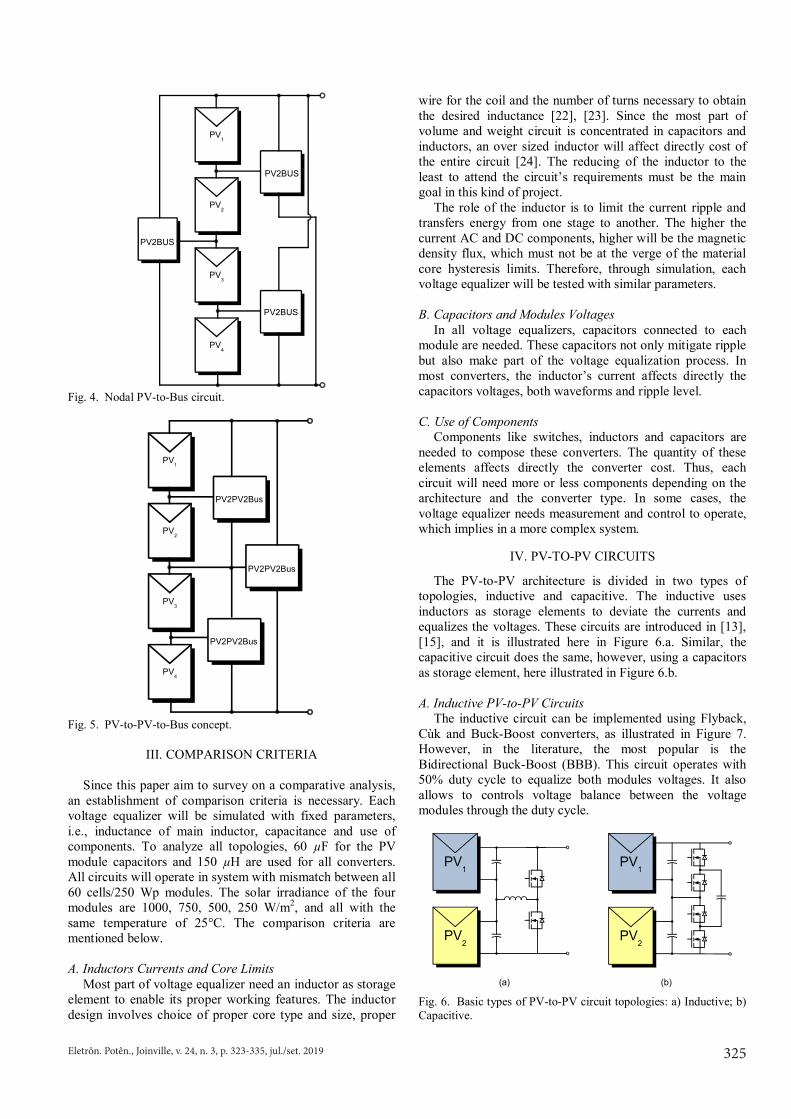
The PV-to-Bus architecture converters process the partial power correspondent to the mismatch from each module to the bus of the string. This architecture can appear in two forms, here, denominated modular and nodal. The modular PV-to-Bus requires one converter per module and it is illustrated in Figure 3. The nodal PV-to-Bus requires one converter per node between each pair of modules and it is illustrated in Figure 4. This architecture can be implemented using various types of converters, i.e Flyback, Buck-Boost and Voltage Multiplier.
Fig. 2. Concept of PV-to-PV Architecture.
Fig. 3. Modular PV-to-Bus circuit. C. PV-to-PV-to-Bus Architecture
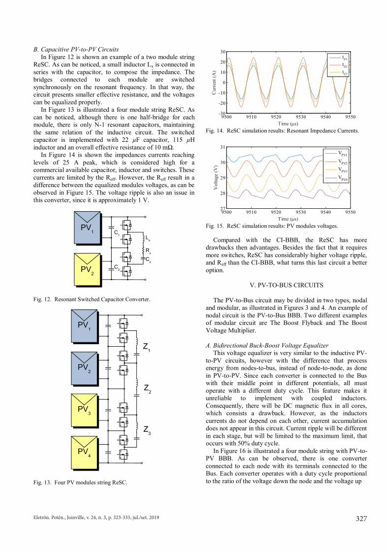
The PV-to-PV-to-Bus is a combination of PV-to-PV and PV-to-Bus architectures. As a hybrid circuit, it sums advantages of both architectures. It is actually a modification of the PV-to-PV architecture to overcome a problem of PV-to-PV circuits, known as current dependence between levels according to [10] or current accumulation according to [21]. For each PV-to-PV circuit there is an equivalent PV-to-PV-to-Bus circuit, [11]. In Figure 4 an example of the PV-to-PV-to-Bus basic concept is illustrated. As can be noticed, some converters are connected PV-to-PV like, and others PV-to-Bus like.
It is important to mention that, no matter the architecture, all voltage equalizers must be based on bidirectional converters to be capable to manage power in both directions. It is also desirable to have step-up and step down characteristics to enable control of each module voltage.
Eletrôn. Potên., Joinville, v. 24, n. 3, p. 323-335, jul./set. 2019 325
There is a three types of architectures and a variety of voltage equalizers circuits in the literature. Thus, in this work is aimed to clarify to the reader the main voltage equalizers advantages and drawbacks compared with each other a comparative study is realized. The criteria for comparison are based in simulation results, using PSIM® software, experimental results, and through design feature analysis. II. LITERATURE VOLTAGE EQUALIZERS ARCHITECTURES
This section presents a brief overview of various voltage equalizers concerning their architecture and the based converter used to implement each circuit. More details are shown in a specific section for each architecture.
The voltage equalizers can be divided in three architectures types, different by the way the partial power is processed, and denominated PV-to-PV, PV-to-Bus and PV-to-PV-to-Bus, [11]. A. PV-to-PV Architecture
The PV-to-PV architecture consists of an array of converters connected between each pair of module. This architecture process the energy from one PV module to the neighboring modules. Figure 2 illustrates the PV-to-PV basic structure. As can be noticed, between each pair of modules there is converter capable to equalize these two modules voltages. For N modules array, N-1 converters are needed to implement this architecture. This architecture can be implemented using two basic types of converters, inductive and capacitive.
The converters topology used to implement the inductive PV-to-PV circuits are Buck-Boost, Flyback and Cùk, [12]. However, in the literature only Buck-Boost converter is commonly found, like in [13]–[15]. There is also the possibility to use coupled inductors to spare the core from DC magnetic flux, as explored in [12] and more detailed in [16]. Hereafter, the Couple Inductor Bidirectional Buck-Boost (CI-BBB) converter is the option to represent the Inductive PV-to-PV circuits, for comparison to the other circuits, since it’s the most present in the literature.
The capacitive type is based on Switched Capacitor (SC) converters, which eliminate the need for inductors resulting in smaller and more efficient converter. However, as a voltage equalizer, this type appears as resonant converter known as Resonant Switched Capacitor (ReSC), introduced in [17] and developed in [18]–[20]. The resonance is obtained adding a small inductor (air core) in series with the capacitor, which enables the circuit to operate with smaller impedance between modules. Therefore, hereafter, the ReSC is the option for comparison as the Capacitive PV-to-PV.
B. PV-to-Bus Architecture
The PV-to-Bus architecture converters process the partial power correspondent to the mismatch from each module to the bus of the string. This architecture can appear in two forms, here, denominated modular and nodal. The modular PV-to-Bus requires one converter per module and it is illustrated in Figure 3. The nodal PV-to-Bus requires one converter per node between each pair of modules and it is illustrated in Figure 4. This architecture can be implemented using various types of converters, i.e Flyback, Buck-Boost and Voltage Multiplier.
Fig. 2. Concept of PV-to-PV Architecture.
Fig. 3. Modular PV-to-Bus circuit. C. PV-to-PV-to-Bus Architecture
The PV-to-PV-to-Bus is a combination of PV-to-PV and PV-to-Bus architectures. As a hybrid circuit, it sums advantages of both architectures. It is actually a modification of the PV-to-PV architecture to overcome a problem of PV-to-PV circuits, known as current dependence between levels according to [10] or current accumulation according to [21]. For each PV-to-PV circuit there is an equivalent PV-to-PV-to-Bus circuit, [11]. In Figure 4 an example of the PV-to-PV-to-Bus basic concept is illustrated. As can be noticed, some converters are connected PV-to-PV like, and others PV-to-Bus like.
It is important to mention that, no matter the architecture, all voltage equalizers must be based on bidirectional converters to be capable to manage power in both directions. It is also desirable to have step-up and step down characteristics to enable control of each module voltage.
Fig. 4. Nodal PV-to-Bus circuit.
Fig. 5. PV-to-PV-to-Bus concept.
III. COMPARISON CRITERIA Since this paper aim to survey on a comparative analysis,
an establishment of comparison criteria is necessary. Each voltage equalizer will be simulated with fixed parameters, i.e., inductance of main inductor, capacitance and use of components. To analyze all topologies, 60 µF for the PV module capacitors and 150 µH are used for all converters. All circuits will operate in system with mismatch between all 60 cells/250 Wp modules. The solar irradiance of the four modules are 1000, 750, 500, 250 W/m2, and all with the same temperature of 25°C. The comparison criteria are mentioned below. A. Inductors Currents and Core Limits
Most part of voltage equalizer need an inductor as storage element to enable its proper working features. The inductor design involves choice of proper core type and size, proper
wire for the coil and the number of turns necessary to obtain the desired inductance [22], [23]. Since the most part of volume and weight circuit is concentrated in capacitors and inductors, an over sized inductor will affect directly cost of the entire circuit [24]. The reducing of the inductor to the least to attend the circuit’s requirements must be the main goal in this kind of project.
The role of the inductor is to limit the current ripple and transfers energy from one stage to another. The higher the current AC and DC components, higher will be the magnetic density flux, which must not be at the verge of the material core hysteresis limits. Therefore, through simulation, each voltage equalizer will be tested with similar parameters. B. Capacitors and Modules Voltages
In all voltage equalizers, capacitors connected to each module are needed. These capacitors not only mitigate ripple but also make part of the voltage equalization process. In most converters, the inductor’s current affects directly the capacitors voltages, both waveforms and ripple level. C. Use of Components
Components like switches, inductors and capacitors are needed to compose these converters. The quantity of these elements affects directly the converter cost. Thus, each circuit will need more or less components depending on the architecture and the converter type. In some cases, the voltage equalizer needs measurement and control to operate, which implies in a more complex system.
IV. PV-TO-PV CIRCUITS
The PV-to-PV architecture is divided in two types of topologies, inductive and capacitive. The inductive uses inductors as storage elements to deviate the currents and equalizes the voltages. These circuits are introduced in [13], [15], and it is illustrated here in Figure 6.a. Similar, the capacitive circuit does the same, however, using a capacitors as storage element, here illustrated in Figure 6.b.
A. Inductive PV-to-PV Circuits
The inductive circuit can be implemented using Flyback, Cùk and Buck-Boost converters, as illustrated in Figure 7. However, in the literature, the most popular is the Bidirectional Buck-Boost (BBB). This circuit operates with 50% duty cycle to equalize both modules voltages. It also allows to controls voltage balance between the voltage modules through the duty cycle.
Fig. 6. Basic types of PV-to-PV circuit topologies: a) Inductive; b) Capacitive.
PV1
PV2
PV1
PV2
(a) (b)

Eletrôn. Potên., Joinville, v. 24, n. 3, p. 323-335, jul./set. 2019326
An improvement in the BBB is proposed through coupled inductors. In Figure 8 is illustrated the Coupled Inductor - Bidiretional Buck Boost (CI-BBB). This circuit has many advantages compared with the BBB. The coupled inductor enables to eliminate the DC magnetic flux, allowing a smaller core choice. Also, with 180° phase shift between the two bridges, the major part of the AC magnetic flux can be canceled. The BBB has a triangular waveform voltage in the modules capacitors that depends on the DC current mismatch. The CI-BBB has a quadratic waveform voltage that depends only on the AC inductor current. Therefore, the CI-BBB has a limited and significant reduced voltage ripple compared to BBB. In summary, the CI-BBB is the best option since it requires smaller inductor and capacitor for the same feature.
In Figure 9 is illustrated a four module string with CI-BBB voltage equalizer. A simulation of this array is made with 25°C module temperature, and solar irradiation of 1000, 750, 500 and 250 W/m2 in modules PV1, PV2, PV3 and PV4, respectively. These input parameters are used in all voltage equalizer simulations hereafter for comparison.
In Figure 10, all coupled inductor currents are shown, which is higher than the current mismatch between modules. In this kind of circuit, appears a phenomenon called as deviated current accumulation [21]. Since all inductor DC currents depends on each other, a high level current may appear in these inductors. Due to the coupling, all currents effects in the core are almost eliminated, and a small amount of flux may appear due to parasitic inductances. However, even the flux being fully eliminated, still remains a high level current been conducted by the switches and inductor wires.
In Figure 11, the modules equalized voltages are shown, which have quadratic waveforms. In this simulation example, due to the coupled inductors, the voltage ripple is relatively small, equal or below 10 mV.
Fig. 7. Types of inductive PV-to-PV voltage equalizers.
Fig. 8. Coupled Inductor Bidirectional Buck-Boost (CI-BBB).
Fig. 9. CI-BBB for four PV modules string.
Fig. 10. CI-BBB: Inductors Currents.
Fig. 11. CI-BBB: PV modules voltages.
PV1
PV2
PV3
PV4
FlyBack
Buck-Boost
Cùk
PV1
+
-
+
-
L1
C
CPV
2
L2
PV1
PV2
PV3
+
-
+
-
+
-
PV4
IL11
IL21
IL31
IL12
IL22
IL32
+
-
9500 9510 9520 9530 9540 9550-4.5
-4
-3.5
-3
-2.5
Time (s)
Cur
rent
(A)
IL21
IL22
IL31
IL12
IL32
IL11
9500 9510 9520 9530 954029.44
29.445
29.45
Time (s)
Vol
tage
(V)
VPV2
VPV4
VPV3
VPV1
Eletrôn. Potên., Joinville, v. 24, n. 3, p. 323-335, jul./set. 2019 327
An improvement in the BBB is proposed through coupled inductors. In Figure 8 is illustrated the Coupled Inductor - Bidiretional Buck Boost (CI-BBB). This circuit has many advantages compared with the BBB. The coupled inductor enables to eliminate the DC magnetic flux, allowing a smaller core choice. Also, with 180° phase shift between the two bridges, the major part of the AC magnetic flux can be canceled. The BBB has a triangular waveform voltage in the modules capacitors that depends on the DC current mismatch. The CI-BBB has a quadratic waveform voltage that depends only on the AC inductor current. Therefore, the CI-BBB has a limited and significant reduced voltage ripple compared to BBB. In summary, the CI-BBB is the best option since it requires smaller inductor and capacitor for the same feature.
In Figure 9 is illustrated a four module string with CI-BBB voltage equalizer. A simulation of this array is made with 25°C module temperature, and solar irradiation of 1000, 750, 500 and 250 W/m2 in modules PV1, PV2, PV3 and PV4, respectively. These input parameters are used in all voltage equalizer simulations hereafter for comparison.
In Figure 10, all coupled inductor currents are shown, which is higher than the current mismatch between modules. In this kind of circuit, appears a phenomenon called as deviated current accumulation [21]. Since all inductor DC currents depends on each other, a high level current may appear in these inductors. Due to the coupling, all currents effects in the core are almost eliminated, and a small amount of flux may appear due to parasitic inductances. However, even the flux being fully eliminated, still remains a high level current been conducted by the switches and inductor wires.
In Figure 11, the modules equalized voltages are shown, which have quadratic waveforms. In this simulation example, due to the coupled inductors, the voltage ripple is relatively small, equal or below 10 mV.
Fig. 7. Types of inductive PV-to-PV voltage equalizers.
Fig. 8. Coupled Inductor Bidirectional Buck-Boost (CI-BBB).
Fig. 9. CI-BBB for four PV modules string.
Fig. 10. CI-BBB: Inductors Currents.
Fig. 11. CI-BBB: PV modules voltages.
PV1
PV2
PV3
PV4
FlyBack
Buck-Boost
Cùk
PV1
+
-
+
-
L1
C
CPV
2
L2
PV1
PV2
PV3
+
-
+
-
+
-
PV4
IL11
IL21
IL31
IL12
IL22
IL32
+
-
9500 9510 9520 9530 9540 9550-4.5
-4
-3.5
-3
-2.5
Time (s)
Cur
rent
(A)
IL21
IL22
IL31
IL12
IL32
IL11
9500 9510 9520 9530 954029.44
29.445
29.45
Time (s)
Vol
tage
(V)
VPV2
VPV4
VPV3
VPV1
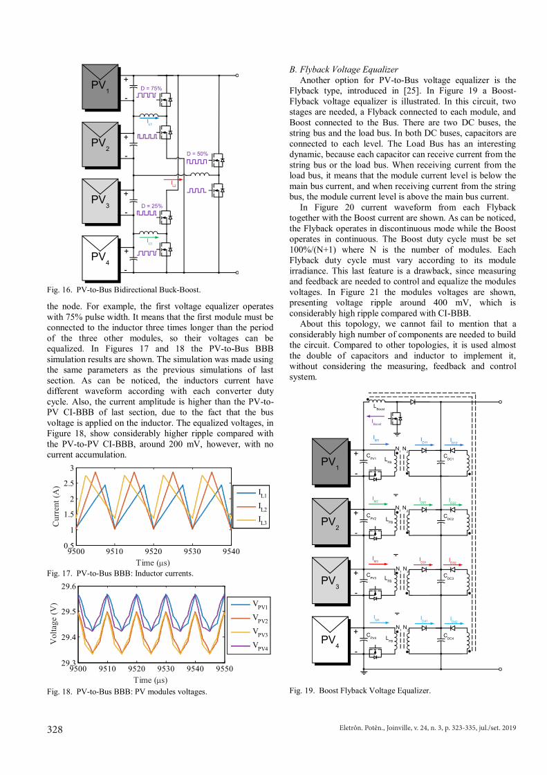
B. Capacitive PV-to-PV Circuits In Figure 12 is shown an example of a two module string
ReSC. As can be noticed, a small inductor Lx is connected in series with the capacitor, to compose the impedance. The bridges connected to each module are switched synchronously on the resonant frequency. In that way, the circuit presents smaller effective resistance, and the voltages can be equalized properly.
In Figure 13 is illustrated a four module string ReSC. As can be noticed, although there is one half-bridge for each module, there is only N-1 resonant capacitors, maintaining the same relation of the inductive circuit. The switched capacitor is implemented with 22 µF capacitor, 115 µH inductor and an overall effective resistance of 10 mΩ.
In Figure 14 is shown the impedances currents reaching levels of 25 A peak, which is considered high for a commercial available capacitor, inductor and switches. These currents are limited by the Reff. However, the Reff result in a difference between the equalized modules voltages, as can be observed in Figure 15. The voltage ripple is also an issue in this converter, since it is approximately 1 V.
Fig. 12. Resonant Switched Capacitor Converter.
Fig. 13. Four PV modules string ReSC.
Fig. 14. ReSC simulation results: Resonant Impedance Currents.
Fig. 15. ReSC simulation results: PV modules voltages.
Compared with the CI-BBB, the ReSC has more drawbacks then advantages. Besides the fact that it requires more switches, ReSC has considerably higher voltage ripple, and Reff than the CI-BBB, what turns this last circuit a better option.
V. PV-TO-BUS CIRCUITS
The PV-to-Bus circuit may be divided in two types, nodal and modular, as illustrated in Figures 3 and 4. An example of nodal circuit is the PV-to-Bus BBB. Two different examples of modular circuit are The Boost Flyback and The Boost Voltage Multiplier. A. Bidirectional Buck-Boost Voltage Equalizer
This voltage equalizer is very similar to the inductive PV-to-PV circuits, however with the difference that process energy from nodes-to-bus, instead of node-to-node, as done in PV-to-PV. Since each converter is connected to the Bus with their middle point in different potentials, all must operate with a different duty cycle. This feature makes it unreliable to implement with coupled inductors. Consequently, there will be DC magnetic flux in all cores, which consists a drawback. However, as the inductors currents do not depend on each other, current accumulation does not appear in this circuit. Current ripple will be different in each stage, but will be limited to the maximum limit, that occurs with 50% duty cycle.
In Figure 16 is illustrated a four module string with PV-to-PV BBB. As can be observed, there is one converter connected to each node with its terminals connected to the Bus. Each converter operates with a duty cycle proportional to the ratio of the voltage down the node and the voltage up
Rx
Cx
Lx
PV1
PV2
C2
C1
PV1
PV2
PV3
PV4
Z1
Z2
Z3
9500 9510 9520 9530 9540 9550-30
-20
-10
0
10
20
30
Time (s)
Cur
rent
(A)
IZ1
IZ2
IZ3
9500 9510 9520 9530 9540 955027
28
29
30
31
Time (s)V
olta
ge (V
)
VPV1
VPV2
VPV3
VPV4
Eletrôn. Potên., Joinville, v. 24, n. 3, p. 323-335, jul./set. 2019328
Fig. 16. PV-to-Bus Bidirectional Buck-Boost.
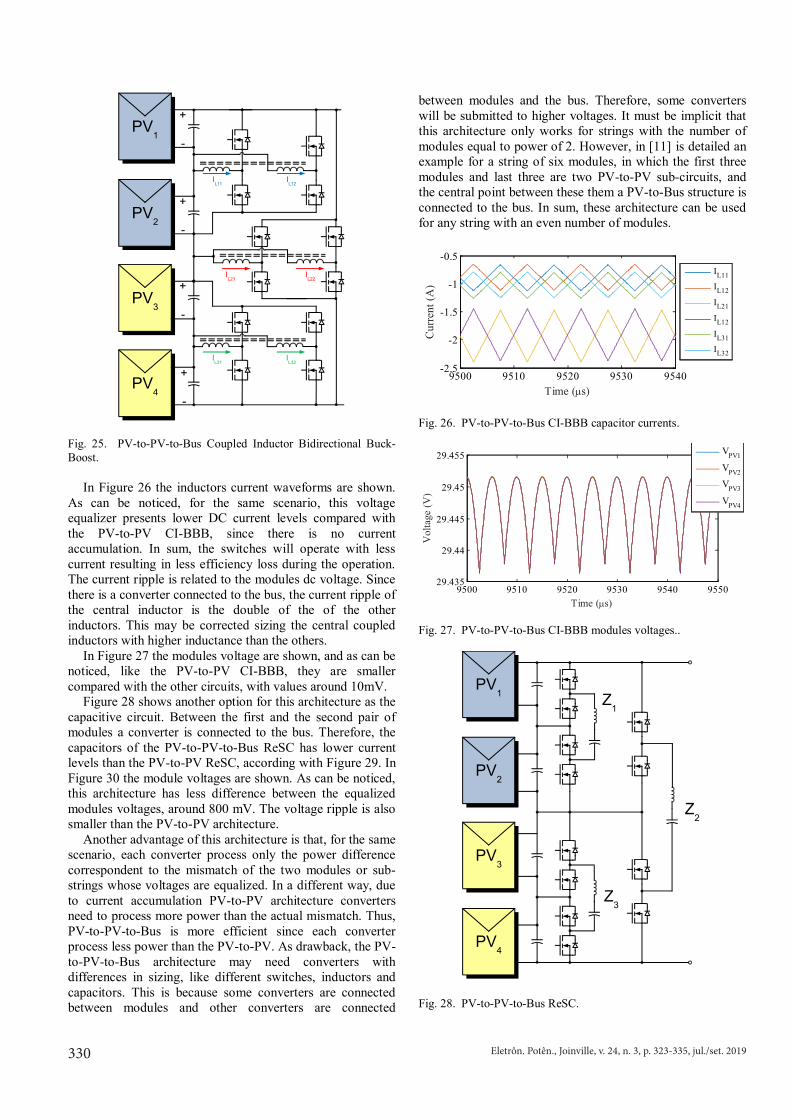
the node. For example, the first voltage equalizer operates with 75% pulse width. It means that the first module must be connected to the inductor three times longer than the period of the three other modules, so their voltages can be equalized. In Figures 17 and 18 the PV-to-Bus BBB simulation results are shown. The simulation was made using the same parameters as the previous simulations of last section. As can be noticed, the inductors current have different waveform according with each converter duty cycle. Also, the current amplitude is higher than the PV-to-PV CI-BBB of last section, due to the fact that the bus voltage is applied on the inductor. The equalized voltages, in Figure 18, show considerably higher ripple compared with the PV-to-PV CI-BBB, around 200 mV, however, with no current accumulation.
Fig. 17. PV-to-Bus BBB: Inductor currents.
Fig. 18. PV-to-Bus BBB: PV modules voltages.
B. Flyback Voltage Equalizer Another option for PV-to-Bus voltage equalizer is the
Flyback type, introduced in [25]. In Figure 19 a Boost-Flyback voltage equalizer is illustrated. In this circuit, two stages are needed, a Flyback connected to each module, and Boost connected to the Bus. There are two DC buses, the string bus and the load bus. In both DC buses, capacitors are connected to each level. The Load Bus has an interesting dynamic, because each capacitor can receive current from the string bus or the load bus. When receiving current from the load bus, it means that the module current level is below the main bus current, and when receiving current from the string bus, the module current level is above the main bus current.
In Figure 20 current waveform from each Flyback together with the Boost current are shown. As can be noticed, the Flyback operates in discontinuous mode while the Boost operates in continuous. The Boost duty cycle must be set 100%/(N+1) where N is the number of modules. Each Flyback duty cycle must vary according to its module irradiance. This last feature is a drawback, since measuring and feedback are needed to control and equalize the modules voltages. In Figure 21 the modules voltages are shown, presenting voltage ripple around 400 mV, which is considerably high ripple compared with CI-BBB.
About this topology, we cannot fail to mention that a considerably high number of components are needed to build the circuit. Compared to other topologies, it is used almost the double of capacitors and inductor to implement it, without considering the measuring, feedback and control system.
Fig. 19. Boost Flyback Voltage Equalizer.
PV1
PV2
PV3
+
-
+
-
+
-
PV4
IL1
IL2
IL3
D = 75%
D = 25%
D = 50%
+
-
9500 9510 9520 9530 95400.5
1
1.5
2
2.5
3
Time (s)
Cur
rent
(A)
IL1
IL2
IL3
9500 9510 9520 9530 9540 955029.3
29.4
29.5
29.6
Time (s)
Vol
tage
(V)
VPV1
VPV2
VPV3
VPV4
PV1
PV2
PV3
+
-
PV4
IM1
+
-
+
-
+
-
LBoost
N1 N
2
N1 N
2
N1 N
2
N1 N
2
LFB
LFB
LFB
LFB
CPV1
CPV2
CPV3
CPV4
CDC1
CDC2
CDC3
CDC4
ID11 I
D12
IM2 I
D21 ID22
IM3 I
D31 ID32
IM4 I
D41 ID42
IBoost

Eletrôn. Potên., Joinville, v. 24, n. 3, p. 323-335, jul./set. 2019 329
Fig. 16. PV-to-Bus Bidirectional Buck-Boost.
the node. For example, the first voltage equalizer operates with 75% pulse width. It means that the first module must be connected to the inductor three times longer than the period of the three other modules, so their voltages can be equalized. In Figures 17 and 18 the PV-to-Bus BBB simulation results are shown. The simulation was made using the same parameters as the previous simulations of last section. As can be noticed, the inductors current have different waveform according with each converter duty cycle. Also, the current amplitude is higher than the PV-to-PV CI-BBB of last section, due to the fact that the bus voltage is applied on the inductor. The equalized voltages, in Figure 18, show considerably higher ripple compared with the PV-to-PV CI-BBB, around 200 mV, however, with no current accumulation.
Fig. 17. PV-to-Bus BBB: Inductor currents.
Fig. 18. PV-to-Bus BBB: PV modules voltages.
B. Flyback Voltage Equalizer Another option for PV-to-Bus voltage equalizer is the
Flyback type, introduced in [25]. In Figure 19 a Boost-Flyback voltage equalizer is illustrated. In this circuit, two stages are needed, a Flyback connected to each module, and Boost connected to the Bus. There are two DC buses, the string bus and the load bus. In both DC buses, capacitors are connected to each level. The Load Bus has an interesting dynamic, because each capacitor can receive current from the string bus or the load bus. When receiving current from the load bus, it means that the module current level is below the main bus current, and when receiving current from the string bus, the module current level is above the main bus current.
In Figure 20 current waveform from each Flyback together with the Boost current are shown. As can be noticed, the Flyback operates in discontinuous mode while the Boost operates in continuous. The Boost duty cycle must be set 100%/(N+1) where N is the number of modules. Each Flyback duty cycle must vary according to its module irradiance. This last feature is a drawback, since measuring and feedback are needed to control and equalize the modules voltages. In Figure 21 the modules voltages are shown, presenting voltage ripple around 400 mV, which is considerably high ripple compared with CI-BBB.
About this topology, we cannot fail to mention that a considerably high number of components are needed to build the circuit. Compared to other topologies, it is used almost the double of capacitors and inductor to implement it, without considering the measuring, feedback and control system.
Fig. 19. Boost Flyback Voltage Equalizer.
PV1
PV2
PV3
+
-
+
-
+
-
PV4
IL1
IL2
IL3
D = 75%
D = 25%
D = 50%
+
-
9500 9510 9520 9530 95400.5
1
1.5
2
2.5
3
Time (s)
Cur
rent
(A)
IL1
IL2
IL3
9500 9510 9520 9530 9540 955029.3
29.4
29.5
29.6
Time (s)
Vol
tage
(V)
VPV1
VPV2
VPV3
VPV4
PV1
PV2
PV3
+
-
PV4
IM1
+
-
+
-
+
-
LBoost
N1 N
2
N1 N
2
N1 N
2
N1 N
2
LFB
LFB
LFB
LFB
CPV1
CPV2
CPV3
CPV4
CDC1
CDC2
CDC3
CDC4
ID11 I
D12
IM2 I
D21 ID22
IM3 I
D31 ID32
IM4 I
D41 ID42
IBoost
Fig. 20. Boost-Flyback simulation results: Inductor currents.
Fig. 21. Boost Flyback simulation results: PV modules voltages. C. Boost Capacitive Voltage Multiplier
Figure 22 illustrates the Boost Capacitive Voltage Multiplier, introduced in [26], which requires only one switch for the entire circuit to operate. This circuit works as a boost connected to all modules through bypass capacitors. Each capacitor delivers energy to the inductor connected to the module. A diode is necessary to enable one way only to charge the module capacitor. In summary, this Voltage Equalizer boost the voltages using a capacitive coupling. But only the lower voltage modules has their capacitor charged through the inductor.
Fig. 22. Boost Capacitive Voltage Multiplier.
Fig. 23. BCVM simulation results: Inductors currents.
Fig. 24. BCVM simulation results: PV modules voltages.
Figure 23 shows module inductor current for this voltage equalizer. As can be noticed, all inductors will have a DC current correspondent to the mismatch of that module to the string. The AC inductor’s current follows the boost current. Like the Flyback circuit, a four module string needs 20% duty cycle.
Figure 24. shows modules voltages during operation. Although equalized, the voltages has different ripple, varying from 150 mV to 700 mV, which are considerably high compared with the previous circuits. A difference between equalized voltages also appear, although is masked by the rippled, and cannot be eliminated, since the circuit control only one switch for the entire voltage equalizer.
Another concern is that, although spare only on switch, it waste cost in bypass capacitors, which must be carefully sized, since they process the power correspondent to mismatch.
VI. PV-TO-PV-TO-BUS CIRCUITS
The PV-to-PV-to-Bus circuits represents a hybrid architecture with advantages of both mentioned. Circuit of this architecture appears in [21], [27] with no mention of been hybrid, which is denominated in [11]. In fact, in this last is shown that, for each PV-to-PV circuit there is a PV-to-PV-to-Bus adaptation that results in no current accumulation. For that reason, its also divided in capacitive and inductive type, which consists an adaptation of CI-BBB e ReSC to operate without current accumulation.
A. CI-BBB / PV-to-PV-to-Bus In Figure 25 is shown the CI-BBB adaptation for the PV-
to-PV-to-Bus architecture. As can be noticed, two converters are connected between modules, and one is connected to the bus. In this way, coupled inductors can be used for circuit implementation since all half-bridges switch with 50% duty cycle, and thus, accumulating advantages of PV-to-PV and PV-to-Bus.
9500 9510 9520 9530 9540 95500
5
10
15
20
25
Time (s)
Cur
rent
(A)
IS1
IS2
IS3
IS4
IBoost
9500 9510 9520 9530 9540 955028.8
29
29.2
29.4
29.6
29.8
Time (s)
Vol
tage
(V)
VPV1
VPV2
VPV3
VPV4
PV1
PV2
PV3
+
-
+
-
+
-
PV4
CB1
CPV1
CB2
CPV2
CB3
CPV3
CB4
CPV4+
-
LB
L1
L2
L3
L4
IL1
IL2
IL3
IL4
ILB
9500 9510 9520 9530 9540 9550
2
4
6
8
Time (s)
Cur
rent
(A)
IL1
IL2
IL3
IL4
9500 9510 9520 9530 954029
29.5
30
Time (s)V
olta
ge (V
)
VPV1
VPV2
VPV3
VPV4
Eletrôn. Potên., Joinville, v. 24, n. 3, p. 323-335, jul./set. 2019330
Fig. 25. PV-to-PV-to-Bus Coupled Inductor Bidirectional Buck-Boost.
In Figure 26 the inductors current waveforms are shown. As can be noticed, for the same scenario, this voltage equalizer presents lower DC current levels compared with the PV-to-PV CI-BBB, since there is no current accumulation. In sum, the switches will operate with less current resulting in less efficiency loss during the operation. The current ripple is related to the modules dc voltage. Since there is a converter connected to the bus, the current ripple of the central inductor is the double of the of the other inductors. This may be corrected sizing the central coupled inductors with higher inductance than the others.
In Figure 27 the modules voltage are shown, and as can be noticed, like the PV-to-PV CI-BBB, they are smaller compared with the other circuits, with values around 10mV.
Figure 28 shows another option for this architecture as the capacitive circuit. Between the first and the second pair of modules a converter is connected to the bus. Therefore, the capacitors of the PV-to-PV-to-Bus ReSC has lower current levels than the PV-to-PV ReSC, according with Figure 29. In Figure 30 the module voltages are shown. As can be noticed, this architecture has less difference between the equalized modules voltages, around 800 mV. The voltage ripple is also smaller than the PV-to-PV architecture.
Another advantage of this architecture is that, for the same scenario, each converter process only the power difference correspondent to the mismatch of the two modules or sub-strings whose voltages are equalized. In a different way, due to current accumulation PV-to-PV architecture converters need to process more power than the actual mismatch. Thus, PV-to-PV-to-Bus is more efficient since each converter process less power than the PV-to-PV. As drawback, the PV-to-PV-to-Bus architecture may need converters with differences in sizing, like different switches, inductors and capacitors. This is because some converters are connected between modules and other converters are connected
between modules and the bus. Therefore, some converters will be submitted to higher voltages. It must be implicit that this architecture only works for strings with the number of modules equal to power of 2. However, in [11] is detailed an example for a string of six modules, in which the first three modules and last three are two PV-to-PV sub-circuits, and the central point between these them a PV-to-Bus structure is connected to the bus. In sum, these architecture can be used for any string with an even number of modules.
Fig. 26. PV-to-PV-to-Bus CI-BBB capacitor currents.
Fig. 27. PV-to-PV-to-Bus CI-BBB modules voltages..
Fig. 28. PV-to-PV-to-Bus ReSC.
PV1
PV2
PV3
+
-
+
-
+
-
PV4
IL11
IL21
IL31
IL12
IL22
IL32
+
-
9500 9510 9520 9530 9540-2.5
-2
-1.5
-1
-0.5
Time (s)
Cur
rent
(A)
IL11
IL12
IL21
IL12
IL31
IL32
9500 9510 9520 9530 9540 955029.435
29.44
29.445
29.45
29.455
Time (s)
Vol
tage
(V)
VPV1
VPV2
VPV3
VPV4
PV1
PV2
PV3
PV4
Z1
Z3
Z2

Eletrôn. Potên., Joinville, v. 24, n. 3, p. 323-335, jul./set. 2019 331
Fig. 25. PV-to-PV-to-Bus Coupled Inductor Bidirectional Buck-Boost.
In Figure 26 the inductors current waveforms are shown. As can be noticed, for the same scenario, this voltage equalizer presents lower DC current levels compared with the PV-to-PV CI-BBB, since there is no current accumulation. In sum, the switches will operate with less current resulting in less efficiency loss during the operation. The current ripple is related to the modules dc voltage. Since there is a converter connected to the bus, the current ripple of the central inductor is the double of the of the other inductors. This may be corrected sizing the central coupled inductors with higher inductance than the others.
In Figure 27 the modules voltage are shown, and as can be noticed, like the PV-to-PV CI-BBB, they are smaller compared with the other circuits, with values around 10mV.
Figure 28 shows another option for this architecture as the capacitive circuit. Between the first and the second pair of modules a converter is connected to the bus. Therefore, the capacitors of the PV-to-PV-to-Bus ReSC has lower current levels than the PV-to-PV ReSC, according with Figure 29. In Figure 30 the module voltages are shown. As can be noticed, this architecture has less difference between the equalized modules voltages, around 800 mV. The voltage ripple is also smaller than the PV-to-PV architecture.
Another advantage of this architecture is that, for the same scenario, each converter process only the power difference correspondent to the mismatch of the two modules or sub-strings whose voltages are equalized. In a different way, due to current accumulation PV-to-PV architecture converters need to process more power than the actual mismatch. Thus, PV-to-PV-to-Bus is more efficient since each converter process less power than the PV-to-PV. As drawback, the PV-to-PV-to-Bus architecture may need converters with differences in sizing, like different switches, inductors and capacitors. This is because some converters are connected between modules and other converters are connected
between modules and the bus. Therefore, some converters will be submitted to higher voltages. It must be implicit that this architecture only works for strings with the number of modules equal to power of 2. However, in [11] is detailed an example for a string of six modules, in which the first three modules and last three are two PV-to-PV sub-circuits, and the central point between these them a PV-to-Bus structure is connected to the bus. In sum, these architecture can be used for any string with an even number of modules.
Fig. 26. PV-to-PV-to-Bus CI-BBB capacitor currents.
Fig. 27. PV-to-PV-to-Bus CI-BBB modules voltages..
Fig. 28. PV-to-PV-to-Bus ReSC.
PV1
PV2
PV3
+
-
+
-
+
-
PV4
IL11
IL21
IL31
IL12
IL22
IL32
+
-
9500 9510 9520 9530 9540-2.5
-2
-1.5
-1
-0.5
Time (s)
Cur
rent
(A)
IL11
IL12
IL21
IL12
IL31
IL32
9500 9510 9520 9530 9540 955029.435
29.44
29.445
29.45
29.455
Time (s)
Vol
tage
(V)
VPV1
VPV2
VPV3
VPV4
PV1
PV2
PV3
PV4
Z1
Z3
Z2
Fig. 29. PV-to-PV-to-Bus ReSC capacitor currents.
Fig. 30. PV-to-PV-to-Bus ReSC modules voltages.
VII. MATHEMATICAL MODELS FOR EACH ARCHITECTURE
Although the simulation results shown a general
perspective of each voltage equalizer and each architecture, mathematical models provide a clear insight for comparison of these circuits. Thus, in this section, a brief analysis of each architecture mathematical model is reproduced. It will be used as example the Bidirectional Buck-Boost Voltage Equalizer for comparison purpose, which appears in all architectures.
A. PV-to-Bus BBB Mathematical Model
In [28], mathematical models of various voltage equalizer are introduced, including PV-to-Bus BBB and PV-to-PV BBB. Based on this study, the inductor currents of a four module string using a PV-to-Bus BBB can be expressed by eq. (1),
(1)
where IL1, IL2 and IL3 represents the inductor currents, D1, D2 and D3 represents each converter duty-cycle, Imain represents the output or string current (which correspond to media of all modules currents), and IPV1, IPV2, IPV3 and IPV4 are the module currents. It can be noticed, observing the A matrix of this linear system, that the inductor current are totally independent of each other. In other words, it is not affected by current accumulation.
As an example, considering the same scenario used in simulation, having IPV1 as 1.8 A, IPV2 as 4.5 A, IPV3 as 7.2 A and IPV4 as 9, and knowing that to operate properly, D1, D2
and D3, must be, respectively, 0.25, 0.50 and 0.75, the inductor currents can be calculated as following by eq. (2).
11
2
3
1 0 0 0 2.25 2.250 1 0 0 2.25 2.250 0 1 0 2.25 2.25
0.25 0.5 0.75 1 9 5.625
L
L
L
main
II
AII
.
(2)
Since there is no current accumulation, all inductor current are equal to the mismatch current between the respectively converter adjacent to the modules. Also, the output current Imain, will always be near the media of all modules currents, independently of the architecture or topology, not considering the losses or malfunction. B. PV-to-PV BBB Mathematical Model
Considering the mathematical model for PV-to-PV BBB, also introduced in [28], its inductor and main current can be calculated using eq. (3).
1 2 12
2 3 21 3
3 4 32
43
1 1 0 01 1 0
0 1 00 0 1
L PV PV
L PV PV
L PV PV
main PV
I I IDI I ID DI I ID
I ID
.
(3)
As can be noticed in this matrix, there is a strong dependency between inductor currents, which results in current accumulation. Unlike the last subsection, in this circuit, the D1, D2 and D3 are all set to 0.5. This last feature enables easier implementation of gatedrivers, when compared with the PV-to-Bus BBB. By solving this linear system for the same scenario, it is found inductor currents with many times superior to the PV-to-Bus BBB, due to current accumulation. This fact turns the PV-to-PV BBB a less efficient option, since ohmic losses will many times higher due to higher current switching.
11
2
3
1 0.5 0 0 2.25 6.750.5 1 0.5 0 2.25 90 0.5 1 0 2.25 6.750 0 0.5 1 9 5.625
L
L
L
main
II
AII
.
(4)
C. PV-to-PV-to-Bus BBB Mathematical Model The PV-to-PV-to-Bus BBB mathematical is introduced
[11], and is repeated here in eq. (5),
1 2 1
2 3 2
3 4 3
1 2 2 3 2 4
1 0 0 00 1 0 00 0 1 0
1 1 1
L PV PV
L PV PV
L PV PV
main PV
I I II I II I I
D D D D D I I
.
(5)
This linear system can be solved for the same scenario of the other architectures, also with D1, D2 and D3 set to 0.5. Here, the result is presented in eq (6).
11
2
3
1 0 0 0 2.25 2.250 1 0 0 2.25 2.250 0 1 0 2.25 2.25
0.25 0.5 0.75 1 9 5.625
L
L
L
main
II
AI
I
(6)
As can be noticed, in this matrix, there is no dependence between inductor currents, what makes this circuit not
9500 9510 9520 9530 9540 9550-15
-10
-5
0
5
10
15
Time (s)
Cur
rent
(A)
IZ1
IZ2
IZ3
9500 9510 9520 9530 9540 955028.8
29
29.2
29.4
29.6
29.8
Time (s)
Vol
tage
(V)
VPV1
VPV2
VPV3
VPV4
1 2 1
2 3 2
3 4 3
1 2 3 4
1 0 0 00 1 0 00 0 1 0
1
L PV PV
L PV PV
L PV PV
main PV
I I II I II I I
D D D I I
Eletrôn. Potên., Joinville, v. 24, n. 3, p. 323-335, jul./set. 2019332
affected by current accumulation, what submit the switches to the same current level of PV-to-Bus. With all duty cycles set to 0.5, it is easier to implement the gatedrivers, like PV-to-PV. In sum, the PV-to-PV-to-Bus presents advantages of both architectures.
In Table I, is shown a comparison of the inductor and main currents for the three architectures of BBB. As can be concluded, PV-to-PV presents inductor current many times higher of the other architecture, leading to higher conductive losses. Another aspect that must reinforced is the fact that both PV-to-PV and PV-to-PV-to-Bus can operate um 50% duty cycle switching, which enables the use of coupled inductors, reducing its volumes, its core losses, and modules voltage ripple.
Table I
Inductor Currents and Output Current for each Architecture Architecture PV-to-Bus PV-to-PV PV-to-PV-to-Bus
IL1 2.25 A 6.75 A 2.25 A
IL2 2.25 A 9 A 2.25 A
IL3 2.25 A 6.75 A 2.25 A
Imain 5.625 A 5.625 A 5.625 A VIII. SUMMARY OF BENEFITS AND DRAWBACKS OF
EACH VOLTAGE EQUALIZER
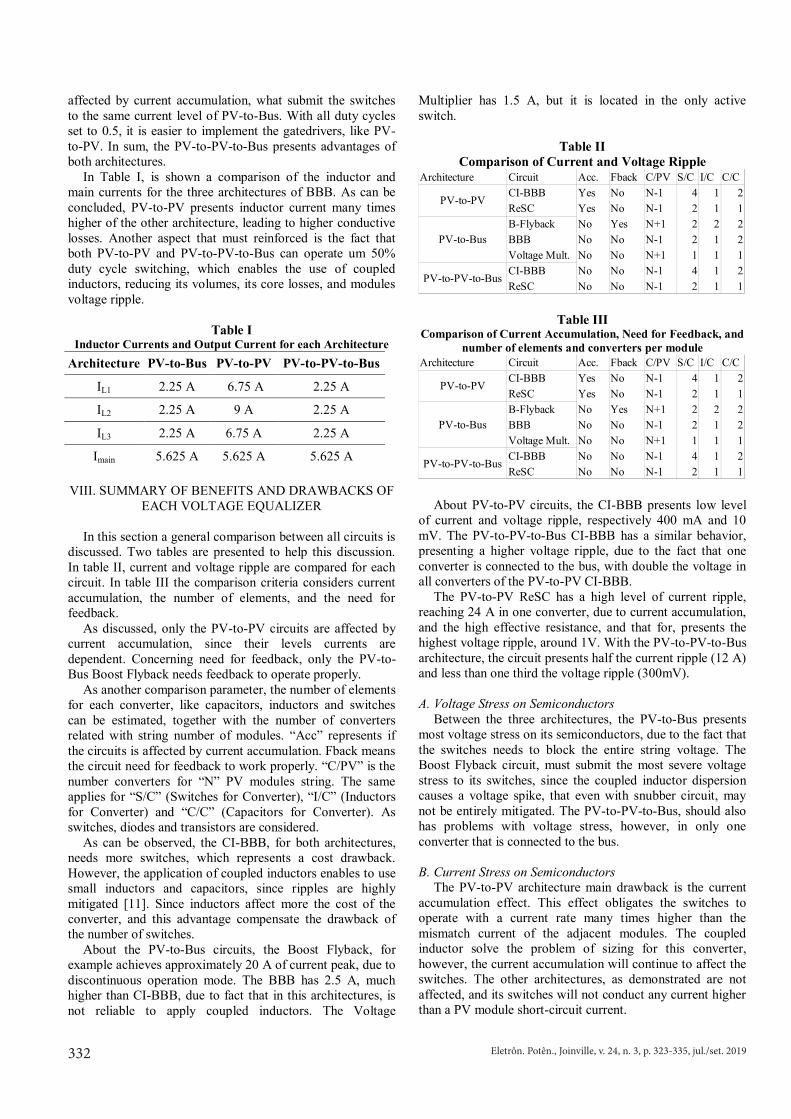
In this section a general comparison between all circuits is discussed. Two tables are presented to help this discussion. In table II, current and voltage ripple are compared for each circuit. In table III the comparison criteria considers current accumulation, the number of elements, and the need for feedback.
As discussed, only the PV-to-PV circuits are affected by current accumulation, since their levels currents are dependent. Concerning need for feedback, only the PV-to-Bus Boost Flyback needs feedback to operate properly.
As another comparison parameter, the number of elements for each converter, like capacitors, inductors and switches can be estimated, together with the number of converters related with string number of modules. “Acc” represents if the circuits is affected by current accumulation. Fback means the circuit need for feedback to work properly. “C/PV” is the number converters for “N” PV modules string. The same applies for “S/C” (Switches for Converter), “I/C” (Inductors for Converter) and “C/C” (Capacitors for Converter). As switches, diodes and transistors are considered.
As can be observed, the CI-BBB, for both architectures, needs more switches, which represents a cost drawback. However, the application of coupled inductors enables to use small inductors and capacitors, since ripples are highly mitigated [11]. Since inductors affect more the cost of the converter, and this advantage compensate the drawback of the number of switches.
About the PV-to-Bus circuits, the Boost Flyback, for example achieves approximately 20 A of current peak, due to discontinuous operation mode. The BBB has 2.5 A, much higher than CI-BBB, due to fact that in this architectures, is not reliable to apply coupled inductors. The Voltage
Multiplier has 1.5 A, but it is located in the only active switch.
Table II
Comparison of Current and Voltage Ripple
Table III Comparison of Current Accumulation, Need for Feedback, and
number of elements and converters per module
About PV-to-PV circuits, the CI-BBB presents low level of current and voltage ripple, respectively 400 mA and 10 mV. The PV-to-PV-to-Bus CI-BBB has a similar behavior, presenting a higher voltage ripple, due to the fact that one converter is connected to the bus, with double the voltage in all converters of the PV-to-PV CI-BBB.
The PV-to-PV ReSC has a high level of current ripple, reaching 24 A in one converter, due to current accumulation, and the high effective resistance, and that for, presents the highest voltage ripple, around 1V. With the PV-to-PV-to-Bus architecture, the circuit presents half the current ripple (12 A) and less than one third the voltage ripple (300mV).
A. Voltage Stress on Semiconductors
Between the three architectures, the PV-to-Bus presents most voltage stress on its semiconductors, due to the fact that the switches needs to block the entire string voltage. The Boost Flyback circuit, must submit the most severe voltage stress to its switches, since the coupled inductor dispersion causes a voltage spike, that even with snubber circuit, may not be entirely mitigated. The PV-to-PV-to-Bus, should also has problems with voltage stress, however, in only one converter that is connected to the bus.
B. Current Stress on Semiconductors
The PV-to-PV architecture main drawback is the current accumulation effect. This effect obligates the switches to operate with a current rate many times higher than the mismatch current of the adjacent modules. The coupled inductor solve the problem of sizing for this converter, however, the current accumulation will continue to affect the switches. The other architectures, as demonstrated are not affected, and its switches will not conduct any current higher than a PV module short-circuit current.
Architecture Circuit Acc. Fback C/PV S/C I/C C/C
PV-to-PVCI-BBB Yes No N-1 4 1 2ReSC Yes No N-1 2 1 1
PV-to-BusB-Flyback No Yes N+1 2 2 2BBB No No N-1 2 1 2Voltage Mult. No No N+1 1 1 1
PV-to-PV-to-BusCI-BBB No No N-1 4 1 2ReSC No No N-1 2 1 1
Architecture Circuit Acc. Fback C/PV S/C I/C C/C
PV-to-PVCI-BBB Yes No N-1 4 1 2ReSC Yes No N-1 2 1 1
PV-to-BusB-Flyback No Yes N+1 2 2 2BBB No No N-1 2 1 2Voltage Mult. No No N+1 1 1 1
PV-to-PV-to-BusCI-BBB No No N-1 4 1 2ReSC No No N-1 2 1 1

Eletrôn. Potên., Joinville, v. 24, n. 3, p. 323-335, jul./set. 2019 333
affected by current accumulation, what submit the switches to the same current level of PV-to-Bus. With all duty cycles set to 0.5, it is easier to implement the gatedrivers, like PV-to-PV. In sum, the PV-to-PV-to-Bus presents advantages of both architectures.
In Table I, is shown a comparison of the inductor and main currents for the three architectures of BBB. As can be concluded, PV-to-PV presents inductor current many times higher of the other architecture, leading to higher conductive losses. Another aspect that must reinforced is the fact that both PV-to-PV and PV-to-PV-to-Bus can operate um 50% duty cycle switching, which enables the use of coupled inductors, reducing its volumes, its core losses, and modules voltage ripple.
Table I
Inductor Currents and Output Current for each Architecture Architecture PV-to-Bus PV-to-PV PV-to-PV-to-Bus
IL1 2.25 A 6.75 A 2.25 A
IL2 2.25 A 9 A 2.25 A
IL3 2.25 A 6.75 A 2.25 A
Imain 5.625 A 5.625 A 5.625 A VIII. SUMMARY OF BENEFITS AND DRAWBACKS OF
EACH VOLTAGE EQUALIZER
In this section a general comparison between all circuits is discussed. Two tables are presented to help this discussion. In table II, current and voltage ripple are compared for each circuit. In table III the comparison criteria considers current accumulation, the number of elements, and the need for feedback.
As discussed, only the PV-to-PV circuits are affected by current accumulation, since their levels currents are dependent. Concerning need for feedback, only the PV-to-Bus Boost Flyback needs feedback to operate properly.
As another comparison parameter, the number of elements for each converter, like capacitors, inductors and switches can be estimated, together with the number of converters related with string number of modules. “Acc” represents if the circuits is affected by current accumulation. Fback means the circuit need for feedback to work properly. “C/PV” is the number converters for “N” PV modules string. The same applies for “S/C” (Switches for Converter), “I/C” (Inductors for Converter) and “C/C” (Capacitors for Converter). As switches, diodes and transistors are considered.
As can be observed, the CI-BBB, for both architectures, needs more switches, which represents a cost drawback. However, the application of coupled inductors enables to use small inductors and capacitors, since ripples are highly mitigated [11]. Since inductors affect more the cost of the converter, and this advantage compensate the drawback of the number of switches.
About the PV-to-Bus circuits, the Boost Flyback, for example achieves approximately 20 A of current peak, due to discontinuous operation mode. The BBB has 2.5 A, much higher than CI-BBB, due to fact that in this architectures, is not reliable to apply coupled inductors. The Voltage
Multiplier has 1.5 A, but it is located in the only active switch.
Table II
Comparison of Current and Voltage Ripple
Table III Comparison of Current Accumulation, Need for Feedback, and
number of elements and converters per module
About PV-to-PV circuits, the CI-BBB presents low level of current and voltage ripple, respectively 400 mA and 10 mV. The PV-to-PV-to-Bus CI-BBB has a similar behavior, presenting a higher voltage ripple, due to the fact that one converter is connected to the bus, with double the voltage in all converters of the PV-to-PV CI-BBB.
The PV-to-PV ReSC has a high level of current ripple, reaching 24 A in one converter, due to current accumulation, and the high effective resistance, and that for, presents the highest voltage ripple, around 1V. With the PV-to-PV-to-Bus architecture, the circuit presents half the current ripple (12 A) and less than one third the voltage ripple (300mV).
A. Voltage Stress on Semiconductors
Between the three architectures, the PV-to-Bus presents most voltage stress on its semiconductors, due to the fact that the switches needs to block the entire string voltage. The Boost Flyback circuit, must submit the most severe voltage stress to its switches, since the coupled inductor dispersion causes a voltage spike, that even with snubber circuit, may not be entirely mitigated. The PV-to-PV-to-Bus, should also has problems with voltage stress, however, in only one converter that is connected to the bus.
B. Current Stress on Semiconductors
The PV-to-PV architecture main drawback is the current accumulation effect. This effect obligates the switches to operate with a current rate many times higher than the mismatch current of the adjacent modules. The coupled inductor solve the problem of sizing for this converter, however, the current accumulation will continue to affect the switches. The other architectures, as demonstrated are not affected, and its switches will not conduct any current higher than a PV module short-circuit current.
Architecture Circuit Acc. Fback C/PV S/C I/C C/C
PV-to-PVCI-BBB Yes No N-1 4 1 2ReSC Yes No N-1 2 1 1
PV-to-BusB-Flyback No Yes N+1 2 2 2BBB No No N-1 2 1 2Voltage Mult. No No N+1 1 1 1
PV-to-PV-to-BusCI-BBB No No N-1 4 1 2ReSC No No N-1 2 1 1
Architecture Circuit Acc. Fback C/PV S/C I/C C/C
PV-to-PVCI-BBB Yes No N-1 4 1 2ReSC Yes No N-1 2 1 1
PV-to-BusB-Flyback No Yes N+1 2 2 2BBB No No N-1 2 1 2Voltage Mult. No No N+1 1 1 1
PV-to-PV-to-BusCI-BBB No No N-1 4 1 2ReSC No No N-1 2 1 1
C. Efficiency Comparison
The efficiency is particularity of each circuit and may have relation with the architecture. Among the PV-to-Bus, the Boost-Flyback should have a considerably low efficiency, between 70% and 80%, due to snubber and coupled inductor losses, as presented in many works in the literature. The PV-to-PV circuits, although based half and full bridges, which are very efficient, above 90%, will have its efficiency decreased by the current accumulation effect. The PV-to-PV-to-Bus, has high probability to be the best choice considering efficiency, since its not affected by current accumulation.
D. Cost Comparison
Among all components necessary to implement a circuit, inductors present a great part of overall cost. So it can be stated that those circuits which involve coupled inductor will have lower cost, since the magnetic volume can be reduced due to flux cancelation. In this case, the PV-to-Bus, should have considerably higher cost than the other architectures.
The number of switches also play important role in the cost. Since PV-to-PV and PV-to-PV-to-Bus have the same number of switches, the difference between its cost will focus on the current and stress over each switch. Although the PV-to-PV-to-Bus has few switches with voltage stress higher than PV-to-PV, this last one, when affected by current accumulation will need high cost switches to implement. E. Implementation Complexity
Due to the need of feedback, the Boost-Flyback presents the most difficult implementation features. All the other circuits operates with fixed duty cycle. The other PV-to-Bus circuits, the BBB and BCVM operates with duty cycle that varies according to the string configuration. In PV-to-PV and PV-to-PV-to-Bus, all converters operate with 50% duty cycle, enabling easy gatedrivers implementation.
The BCVM presents a particular problem in its implemenation related to the bypass capacitor. This capacitor, must have high values like 220µF each, will work with high current levels, near the modules, and may occupy a significant volume in the circuit.
The ReSC needs careful sizing, since it must operate at the resonance of circuit that is susceptible to 10% tolerance, like the Cx and Lx. Also, all resonant impedances must be as equal as possible, to avoid increase effective resistance and hence difference in equalized voltages.
In summary, based on the circuit properties and the simulation results, and the other factors, it can be stated that the best choice for voltage equalizer implementation recommended is the CI-BBB, rather the PV-to-PV or the PV-to-PV-to-Bus. This is because, if generator has an odd number of modules, the PV-to-PV-to-Bus is not suitable, and the PV-to-PV must be used. However, with pair number of modules, the PV-to-PV-to-Bus will be a better option, since it will not be affected by current accumulation.
XI. EXPERIMENTAL RESULTS In this section is presented an experiment result for the
PV-to-PV CI-BBB compared with PV-to-PV-to-Bus CI-BBB. In this experiment, a four modules string with different irradiances of 780, 770, 540 and 630 W/m2, works as PV generator. The mismatch is emulated through modules disorientation. The same circuit is used to implement both voltage equalizers, only differing in two points of connection for the converter of middle level of the arrange.
Figure 31 shows a picture of one of the three converters used to implement the CI-BBB for both architectures. As can be observed each converter is a full bridge with a coupled inductor in the ac side. A current sensor LA-55P is used to measure the current.
Figure 32 shows inductor currents IL1, IL2 and IL3 for both architecture. The dc component of each current is disposed as dashed line of same color, and also in the legend. As can be noticed, all currents from PV-to-PV is many times higher than PV-to-PV-to-Bus, due to current accumulation. The ripple associated in all currents is caused by stray and parasitic inductance, present in the bridge circuit and the coupled inductor.
Figure 33 shows the equalized voltage for architectures. As can be noticed, the PV-to-PV-to-Bus architecture present low difference between the equalized voltage. This is because low current in the switches, the MOSFETs on resistance voltage drop is smaller since there is no current accumulation. The same, cannot be observed in the PV-to-PV architecture. In fact, this voltage drop could disturb the MPPT algorithm in a way to not find the global MPP.
X. CONCLUSIONS
In this paper, a comparative analysis of various voltage equalizers from different architectures, based in circuit evaluation, simulation and experimental results, is made. First is detailed the three architectures: PV-to-PV, PV-to-Bus and PV-to-PV-to-Bus, pointing out each circuit main advantages and drawbacks. In sequence, some examples of circuits of each architecture are shown, with simulation results using similar parameters for comparison criteria. Also, the mathematical model for a circuit example that appears in all three architectures, help to understand analytically each system. The comparison is based in the current accumulation susceptibility, the number of converters and components for module, and simulation results, more specifically the voltage and current ripple, voltage and current stress, efficiency, cost estimation and implementation complexity. The CI-BBB shows to be an interesting choice, since it is easier to implement, it has reduced cost, and its highly efficient, rather in PV-to-PV or PV-to-PV-to-Bus architecture. PV-to-PV is affected by current accumulation what reduces its efficiency compared with PV-to-PV-to-Bus, submit its switches to higher current levels. Thus, PV-to-PV-to-Bus CI-BBB should be a better option for an even string of modules.

Eletrôn. Potên., Joinville, v. 24, n. 3, p. 323-335, jul./set. 2019334
Fig. 31. Picture of one of the three converters used to implement PV-to-PV CI-BBB and PV-to-PV-to-Bus CI-BBB.
Fig. 32. Inductor currents for both PV-to-PV CI-BBB and PV-to-PV-to-Bus CI-BBB.
Fig. 33. Equalized voltage: (a) PV-to-PV CI-BBB; (b) PV-to-PV-to-Bus CI-BBB.
ACKNOLEDGEMENT
The authors are thankful to CNPq for the financial support
in project, as also the institutions of CEFET-MG and UFMG.
REFERENCES [1] D. S. O. J. Bruno Ricardo de Almeida, “Conversor
CA-CC Trifásico Bidirecional de Único Estágio com Correção de Fator de Potência e Isolado em Alta
Frequência”, in Eletrônica de Potência, vol. 21, no. 2, pp. 117–125, 2016.
[2] M. G. Alves, M. A. G. De Brito, and C. A. Canesin, “Análise de Estruturas Inversoras Não Isoladas Monofásicas Para Geração Distribuídas Fotovoltaica”, in Eletrônica de Potência, vol. 22, no. 2, pp. 179–186, 2017.
[3] P. P. Praça, D. B. S. Alves, D. S. O. Jr, L. C. S. Mazza, and L. H. S. C. Barreto, “Ganho de Tensão para Aplicações em Sistemas Fotovoltaicos”, in Eletrônica de Potência, vol. 22, no. 3, pp. 258–268, 2017.
[4] L. L. Brighenti, A. L. Batschauer, M. Mezaroba, and L. Inverters, “Inversores Comutados pela Rede Associados a um Autotransformador Multipulsos para a Geração”, in Eletrônica de Potência, vol. 21, no. 3, pp. 200–211, 2016.
[5] P. Manganiello, M. Balato, and M. Vitelli, “A Survey on Mismatching and Aging of PV Modules: The Closed Loop”, in IEEE Trans. Ind. Electron., vol. 62, no. 11, pp. 7276–7286, 2015.
[6] U. O. C. C. Ćuk, “Caracterizador elétrico de módulos fotovoltaicos utilizando o conversor cc-cc ćuk”, in Eletrônica de Potência, vol. 22, no. 2, pp. 139–147, 2017.
[7] S. A. Oliveira, L. P. Sampaio, F. M. De Oliveira, and F. R. Durand, “Sistema Fotovoltaico com Condicionamento Ativo de Energia Usando MPPT Baseado em PSO e Malha Feed-Forward”, in Eletrônica de Potência, vol. 21, no. 2, pp. 105–116, 2016.
[8] M. A. G. De A, Carlos Brito, M. G. Alves, R. B. Godoy, and C. A. Canesin, “MPPT Híbrido Aplicado à Associação dos Conversores Boost ZVT e Inversor H6 Para Aplicações Fotovoltaicas”, in Eletrônica de Potência, vol. 23, no. 2, pp. 216–225, 2018.
[9] L. C. Freitas et al., “Algoritmo de Seguimento do Ponto de Máxima Potência Global para Inversores Solares Multistring em Condições de Sombreamento Parcial”, in Eletrônica de Potência, vol. 23, no. 2, pp. 182–192, 2018.
[10] M. Kasper, D. Bortis, and J. W. Kolar, “Classification and comparative evaluation of PV panel-integrated DC-DC converter concepts”, in IEEE Trans. Power Electron., vol. 29, no. 5, pp. 2511–2526, 2014.
[11] C. H. G. Santos, “Desviadores de Corrente de Arquitetura Híbrida Para Compensação de Sombreamento Parcial em Associações Série de Módulos Fotovoltaicos”, UFMG - PPGEE, 2018.
[12] G. R. Walker and J. C. Pierce, “PhotoVoltaic DC-DC module integrated converter for novel cascaded and bypass grid connection topologies - Design and optimisation”, in PESC Rec. - IEEE Annu. Power Electron. Spec. Conf., 2006.
-15 -10 -5 0 5 10 15
0
0.5
1
Cur
rent
(A)
IL1 PV-to-PV
IL1 PV-to-PV-to-Bus
638 mA140 mA
-15 -10 -5 0 5 10 15
0
1
2
3
Cur
rent
(A)
IL2 PV-to-PV
IL2 PV-to-PV-to-Bus
2,09 A1,08 A
-15 -10 -5 0 5 10 15-1
0
1
2
3
Time (s)
Cur
rent
(A)
IL3 PV-to-PV
IL3 PV-to-PV-to-Bus
1,66 A726 mA
160 170 180 190 20019
20
21
22
23
Time (ms)
Volta
ge (V
)
160 170 180 190 20019
20
21
22
23
Time (ms)
Volta
ge (V
)
VPV1VPV2VPV3VPV4

Eletrôn. Potên., Joinville, v. 24, n. 3, p. 323-335, jul./set. 2019 335
Fig. 31. Picture of one of the three converters used to implement PV-to-PV CI-BBB and PV-to-PV-to-Bus CI-BBB.
Fig. 32. Inductor currents for both PV-to-PV CI-BBB and PV-to-PV-to-Bus CI-BBB.
Fig. 33. Equalized voltage: (a) PV-to-PV CI-BBB; (b) PV-to-PV-to-Bus CI-BBB.
ACKNOLEDGEMENT
The authors are thankful to CNPq for the financial support
in project, as also the institutions of CEFET-MG and UFMG.
REFERENCES [1] D. S. O. J. Bruno Ricardo de Almeida, “Conversor
CA-CC Trifásico Bidirecional de Único Estágio com Correção de Fator de Potência e Isolado em Alta
Frequência”, in Eletrônica de Potência, vol. 21, no. 2, pp. 117–125, 2016.
[2] M. G. Alves, M. A. G. De Brito, and C. A. Canesin, “Análise de Estruturas Inversoras Não Isoladas Monofásicas Para Geração Distribuídas Fotovoltaica”, in Eletrônica de Potência, vol. 22, no. 2, pp. 179–186, 2017.
[3] P. P. Praça, D. B. S. Alves, D. S. O. Jr, L. C. S. Mazza, and L. H. S. C. Barreto, “Ganho de Tensão para Aplicações em Sistemas Fotovoltaicos”, in Eletrônica de Potência, vol. 22, no. 3, pp. 258–268, 2017.
[4] L. L. Brighenti, A. L. Batschauer, M. Mezaroba, and L. Inverters, “Inversores Comutados pela Rede Associados a um Autotransformador Multipulsos para a Geração”, in Eletrônica de Potência, vol. 21, no. 3, pp. 200–211, 2016.
[5] P. Manganiello, M. Balato, and M. Vitelli, “A Survey on Mismatching and Aging of PV Modules: The Closed Loop”, in IEEE Trans. Ind. Electron., vol. 62, no. 11, pp. 7276–7286, 2015.
[6] U. O. C. C. Ćuk, “Caracterizador elétrico de módulos fotovoltaicos utilizando o conversor cc-cc ćuk”, in Eletrônica de Potência, vol. 22, no. 2, pp. 139–147, 2017.
[7] S. A. Oliveira, L. P. Sampaio, F. M. De Oliveira, and F. R. Durand, “Sistema Fotovoltaico com Condicionamento Ativo de Energia Usando MPPT Baseado em PSO e Malha Feed-Forward”, in Eletrônica de Potência, vol. 21, no. 2, pp. 105–116, 2016.
[8] M. A. G. De A, Carlos Brito, M. G. Alves, R. B. Godoy, and C. A. Canesin, “MPPT Híbrido Aplicado à Associação dos Conversores Boost ZVT e Inversor H6 Para Aplicações Fotovoltaicas”, in Eletrônica de Potência, vol. 23, no. 2, pp. 216–225, 2018.
[9] L. C. Freitas et al., “Algoritmo de Seguimento do Ponto de Máxima Potência Global para Inversores Solares Multistring em Condições de Sombreamento Parcial”, in Eletrônica de Potência, vol. 23, no. 2, pp. 182–192, 2018.
[10] M. Kasper, D. Bortis, and J. W. Kolar, “Classification and comparative evaluation of PV panel-integrated DC-DC converter concepts”, in IEEE Trans. Power Electron., vol. 29, no. 5, pp. 2511–2526, 2014.
[11] C. H. G. Santos, “Desviadores de Corrente de Arquitetura Híbrida Para Compensação de Sombreamento Parcial em Associações Série de Módulos Fotovoltaicos”, UFMG - PPGEE, 2018.
[12] G. R. Walker and J. C. Pierce, “PhotoVoltaic DC-DC module integrated converter for novel cascaded and bypass grid connection topologies - Design and optimisation”, in PESC Rec. - IEEE Annu. Power Electron. Spec. Conf., 2006.
-15 -10 -5 0 5 10 15
0
0.5
1
Cur
rent
(A)
IL1 PV-to-PV
IL1 PV-to-PV-to-Bus
638 mA140 mA
-15 -10 -5 0 5 10 15
0
1
2
3
Cur
rent
(A)
IL2 PV-to-PV
IL2 PV-to-PV-to-Bus
2,09 A1,08 A
-15 -10 -5 0 5 10 15-1
0
1
2
3
Time (s)
Cur
rent
(A)
IL3 PV-to-PV
IL3 PV-to-PV-to-Bus
1,66 A726 mA
160 170 180 190 20019
20
21
22
23
Time (ms)
Volta
ge (V
)
160 170 180 190 20019
20
21
22
23
Time (ms)
Volta
ge (V
)
VPV1VPV2VPV3VPV4
[13] R. Kadri, J. P. Gaubert, and G. Champenois, “Nondissipative string current diverter for solving the cascaded DC-DC converter connection problem in photovoltaic power generation system”, in IEEE Trans. Power Electron., vol. 27, no. 3, pp. 1249–1258, 2012.
[14] K. Kesarwani, C. Schaef, C. R. Sullivan, and J. T. Stauth, “A multi-level ladder converter supporting vertically-stacked digital voltage domains”, in Conf. Proc. - IEEE Appl. Power Electron. Conf. Expo. - APEC, pp. 429–434, 2013.
[15] R. Kadri, J. P. Gaubert, and G. Champenois, “New converter topology to improve performance of photovoltaic power generation system under shading conditions”, in Int. Conf. Power Eng. Energy Electr. Drives, no. May, pp. 0–6, 2011.
[16] C. Schaef, K. Kesarwani, and J. T. Stauth, “A coupled-inductor multi-level ladder converter for sub-module PV power management”, in Conf. Proc. - IEEE Appl. Power Electron. Conf. Expo. - APEC, pp. 732–737, 2013.
[17] J. T. Stauth, M. D. Seeman, and K. Kesarwani, “A resonant switched-capacitor ic and embedded system for sub-module photovoltaic power management”, in IEEE J. Solid-State Circuits, vol. 47, no. 12, pp. 3043–3054, 2012.
[18] K. Kesarwani, R. Sangwan, and J. T. Stauth, “Resonant switched-capacitor converters for chip-scale power delivery: Modeling and design”, in IEEE 14th Work. Control Model. Power Electron. COMPEL, 2013.
[19] A. Blumenfeld, A. Cervera, and M. M. Peretz, “Enhanced differential power processor for PV systems: Resonant switched-capacitor gyrator converter with local MPPT”, in IEEE J. Emerg. Sel. Top. Power Electron., vol. 2, no. 4, pp. 883–892, 2014.
[20] R. Sangwan, K. Kesarwani, and J. T. Stauth, “High-density power converters for sub-module photovoltaic power management”, in IEEE Energy Convers. Congr. Expo. ECCE, pp. 3279–3286, 2014.
[21] C. H. G. Santos, P. F. Donoso-Garcia, and S. I. S. Júnior, “Cascaded Cell String Current Diverter For Improvement of Photovoltaic Solar Array Under Partial Shading Problems”, in Eletrônica de Potência, vol. 20, no. 3, pp. 272–282, 2015.
[22] S. A. D. Contreras, P. C. Cortizo, and M. A. Severo Mendes, “Simple control technique for interleaved inverters with magnetically coupled legs”, in IET Power Electron., vol. 6, no. 2, pp. 353–363, 2013.
[23] S. A. D. Contreras, “Estudos da Aplicação de Transformadores Intercelulares em Inversores de Tensão”, in Universidade Federal de Minas Gerais, 2014.
[24] L. Crane, “Selecting the best inductor for your DC-
DC converter (469-1)”, in Appl. note, pp. 1–5, 2005. [25] J. H. Park and K. T. Kim, “Multi-output differential
power processing system using boost-flyback converter for voltage balancing”, in Proc. - 2017 Int. Conf. Recent Adv. Signal Process. Telecommun. Comput. SigTelCom 2016, pp. 139–142, 2017.
[26] M. Uno and A. Kukita, “Single-Switch Voltage Equalizer Using Multistacked Buck–Boost Converters for Partially Shaded Photovoltaic Modules”, in IEEE Trans. Power Electron., vol. 30, no. 6, pp. 3091–3105, 2015.
[27] M. Z. Ramli and Z. Salam, “A simple energy recovery scheme to harvest the energy from shaded photovoltaic modules during partial shading”, in IEEE Trans. Power Electron., vol. 29, no. 12, pp. 6458–6471, 2014.
[28] P. S. Shenoy, K. a. Kim, and P. T. Krein, “Comparative analysis of differential power conversion architectures and controls for solar photovoltaics”, in 2012 IEEE 13th Work. Control Model. Power Electron., pp. 1–7, 2012.
BIOGRAPHIES
Cláudio H. G. Santos, was born in October 05, 1982 in Divinópolis, MG – Brazil. Has received his M.Sc and B.Sc. degrees in Electrical Engineering from CEFET-MG and Doctor in Electrical Engineering from UFMG in Belo Horizonte, Brazil in 2008, 2011 and 2018, respectively. Nowadays, he is a teacher member of de Mechatronics Engineer Department of CEFET-MG, located in St. Álvares Azevedo 400, in Divinópolis, Brazil. He also had same position in the Federal University of Outo Preto, MG – Brazil. His currently research interest is power-quality-related issues, solar PV technology, charge stations and electric vehicles.
Pedro Francisco Donoso-Garcia, has graduated inelectrical engineering option in electronics by the Universidade Federal do Rio Grande do Sul – UFRGS in 1981, he received his MSc from the Universidade Federal de Minas Gerais – UFMG and his PhD in Electrical Engineering from the Universidade Federal de Santa Catarina – UFSC in 1986 and 1991 respectively. Currently he is an Associate Professor at the Electronic Engineering Dept.–DELT–UFMG. His research interest include: high efficiency power supply, electronic ballasts and different microgrid aspects, including power electronics and distributed energy-storage systems.
Seleme I. Seleme Jr., was born in Novemeber 03 1955 in Palmas, PR – Brazil. Has graduated in Electrical Engineering from EPUSP at São Paulo in 1977, obtained his M.Sc from UFSC at Florianópolis, in 1985 and his PhD from INPG at Grenoble, France, in 1994. He has made his Post Doctorate at UC Berleley, USA, in 2002. Presently he is an Associate Professor, member of the Electronic Department at the Engineering School, UFMG. His main research interests are power electronics, applied control for static converters, electrical drive systems and electromechanical systems.