A Clock-Tuned Discrete-Time Negative Capacitor Implemented...
5
A Clock-Tuned Discrete-Time Negative Capacitor Implemented Using Analog Samplers Donald M. Johnson InVue Charlotte, NC, USA Email: [email protected] Thomas P. Weldon Department of Electrical and Computer Engineering University of North Carolina at Charlotte Charlotte, NC, USA Abstract—The recent introduction of digital non-Foster circuits offers new methods for implementing negative capacitance and inductance, but may require a high-speed high-resolution digital signal processor, analog-to-digital converter, and digital-to-analog converter. Therefore, an alternative discrete-time design approach is presented, where a clock-tuned negative capacitor is imple- mented using analog samplers. The resulting design requires only two samplers, a differential amplifier, and an operational transconductance amplifier, eliminating the need for a digital signal processor and converters. In addition, it is shown that the negative capacitance can be tuned by the digital clock and is theoretically proportional to the clock period. Experimental results for a prototype demonstrate a tunable capacitance from -2.1 nF to -5.5 nF with |Q| > 2 for signal frequencies below approximately one-tenth of the clock frequency. I. I NTRODUCTION There is renewed interest in the design of non-Foster circuits such as negative capacitors to support important and emerging applications such as electrically-small antennas, metamaterial cloaks, and software defined radios [1]–[5]. Although some successful results have been obtained with analog non-Foster circuits, design issues such as stability remain quite challeng- ing [6], [7]. Recently, digital non-Foster circuits have shown promise as an alternative design approach that may leverage advantages of digital technology for certain applications [8]– [10]. One key advantage of the digital approach is that the Nyquist limit sets an upper frequency bound for any potential instability. However, digital non-Foster circuits may be limited by the need for a high-speed high-resolution digital signal processor, high-speed ADC (analog-to-digital converter), and high-speed DAC (digital-to-analog converter). Therefore, an alternative discrete-time implementation of a digital non-Foster circuit is proposed, where a clock-tuned negative capacitor is implemented using analog samplers, without a signal processor, ADC, or DAC. The proposed circuit consists of two analog samplers, a differential amplifier, and an OTA (operational transconductance amplifier). The clock and a delayed clock set the timing for the samplers, and the frequency of the clock sets the desired capacitance. Although a similar clock-tuned digital non-Foster circuit was given in [11], it required an ADC and DAC. Lastly, depending on the application and implementation, the simplicity and analog nature of the proposed approach may offer the designer advantages in chip area, power consumption, bandwidth, or signal dynamic range. In Section II, theory is presented for the clock-tuned digi- tal negative capacitor. Section III describes simulations and measured results for a prototype, demonstrating a negative capacitance can be clock-tuned from -2.6 nF to -6.2 nF. II. THEORY The proposed implementation of the clock-tuned discrete- time negative capacitor is shown in Fig. 1, where v in (t) is the input voltage, i in (t) is the input current of the system, and Clk1 and Clk2 are digital clock signals at the discrete-time sampling frequency f s =1/T s . The input signal is sampled by a first analog sampler producing discrete-time signal v in [n]= v in (nT s ). This first sampled signal is then sampled by the second analog sampler to produce v in [n - 1]. The output of the difference amplifier is then v in [n] - v in [n - 1], and the output of the OTA becomes the input current of the system i in (nT s )= i in [n]= g m · (v in [n] - v in [n - 1]), where g m is the OTA tranconductance. The timing diagram for the two clock signals of Fig. 1 is shown in Fig. 2. The signal Clk1 provides the clock for the first sampler, while Clk2 provides the clock signal for the second sampler, with both signals at frequency f s . In the prototype, Fig. 1. Block diagram of proposed system, where “Clk1” and “Clk2” are the sampling clocks. Fig. 2. Timing diagram of proposed system, where “Clk1” and “Clk2” are the sampling clocks at frequency fs =1/Ts, and where the pulse width was chosen to be Ts/6 to accommodate board and device limitations.
Transcript of A Clock-Tuned Discrete-Time Negative Capacitor Implemented...
A Clock-Tuned Discrete-Time Negative CapacitorImplemented Using Analog Samplers
Donald M. JohnsonInVue
Charlotte, NC, USAEmail: [email protected]
Thomas P. WeldonDepartment of Electrical and Computer Engineering
University of North Carolina at CharlotteCharlotte, NC, USA
Abstract—The recent introduction of digital non-Foster circuits
offers new methods for implementing negative capacitance and
inductance, but may require a high-speed high-resolution digital
signal processor, analog-to-digital converter, and digital-to-analog
converter. Therefore, an alternative discrete-time design approach
is presented, where a clock-tuned negative capacitor is imple-
mented using analog samplers. The resulting design requires
only two samplers, a differential amplifier, and an operational
transconductance amplifier, eliminating the need for a digital
signal processor and converters. In addition, it is shown that
the negative capacitance can be tuned by the digital clock and
is theoretically proportional to the clock period. Experimental
results for a prototype demonstrate a tunable capacitance from
�2.1 nF to �5.5 nF with |Q| > 2 for signal frequencies below
approximately one-tenth of the clock frequency.
I. INTRODUCTION
There is renewed interest in the design of non-Foster circuitssuch as negative capacitors to support important and emergingapplications such as electrically-small antennas, metamaterialcloaks, and software defined radios [1]–[5]. Although somesuccessful results have been obtained with analog non-Fostercircuits, design issues such as stability remain quite challeng-ing [6], [7]. Recently, digital non-Foster circuits have shownpromise as an alternative design approach that may leverageadvantages of digital technology for certain applications [8]–[10]. One key advantage of the digital approach is that theNyquist limit sets an upper frequency bound for any potentialinstability. However, digital non-Foster circuits may be limitedby the need for a high-speed high-resolution digital signalprocessor, high-speed ADC (analog-to-digital converter), andhigh-speed DAC (digital-to-analog converter).
Therefore, an alternative discrete-time implementation of adigital non-Foster circuit is proposed, where a clock-tunednegative capacitor is implemented using analog samplers,without a signal processor, ADC, or DAC. The proposedcircuit consists of two analog samplers, a differential amplifier,and an OTA (operational transconductance amplifier). Theclock and a delayed clock set the timing for the samplers,and the frequency of the clock sets the desired capacitance.Although a similar clock-tuned digital non-Foster circuit wasgiven in [11], it required an ADC and DAC. Lastly, dependingon the application and implementation, the simplicity andanalog nature of the proposed approach may offer the designer
advantages in chip area, power consumption, bandwidth, orsignal dynamic range.
In Section II, theory is presented for the clock-tuned digi-tal negative capacitor. Section III describes simulations andmeasured results for a prototype, demonstrating a negativecapacitance can be clock-tuned from �2.6 nF to �6.2 nF.
II. THEORY
The proposed implementation of the clock-tuned discrete-time negative capacitor is shown in Fig. 1, where vin(t) is theinput voltage, iin(t) is the input current of the system, andClk1 and Clk2 are digital clock signals at the discrete-timesampling frequency fs = 1/Ts. The input signal is sampled bya first analog sampler producing discrete-time signal vin[n] =vin(nTs). This first sampled signal is then sampled by thesecond analog sampler to produce vin[n � 1]. The output ofthe difference amplifier is then vin[n] � vin[n � 1], and theoutput of the OTA becomes the input current of the systemiin(nTs) = iin[n] = gm · (vin[n]� vin[n� 1]), where gm isthe OTA tranconductance.
The timing diagram for the two clock signals of Fig. 1 isshown in Fig. 2. The signal Clk1 provides the clock for the firstsampler, while Clk2 provides the clock signal for the secondsampler, with both signals at frequency fs. In the prototype,
Fig. 1. Block diagram of proposed system, where “Clk1” and “Clk2” are thesampling clocks.
Fig. 2. Timing diagram of proposed system, where “Clk1” and “Clk2” arethe sampling clocks at frequency fs = 1/Ts, and where the pulse width waschosen to be Ts/6 to accommodate board and device limitations.
Copyright 2018 IEEE. Published in 2018 IEEE Int. Symp. on Circuits and Systems, Florence, Italy, May 27-30, 2018. Personal use of this material is permitted. However, permission to reprint/republish this material for advertising or promotional purposes or for creating new collective works for resale or redistribution to servers or lists, or to reuse any copyrighted component of this work in other works, must be obtained from the IEEE, 445 Hoes Lane,Piscataway, NJ 08855, USA. Tel.: 908-562-3966. See https://ieeexplore.ieee.org/search/searchresult.jsp?newsearch=true&queryText=A%20Clock-Tuned%20Discrete-Time%20Negative%20Capacitor%20Implemented%20Using%20Analog%20Samplers
(a) (b) (c)
(d) (e) (f)
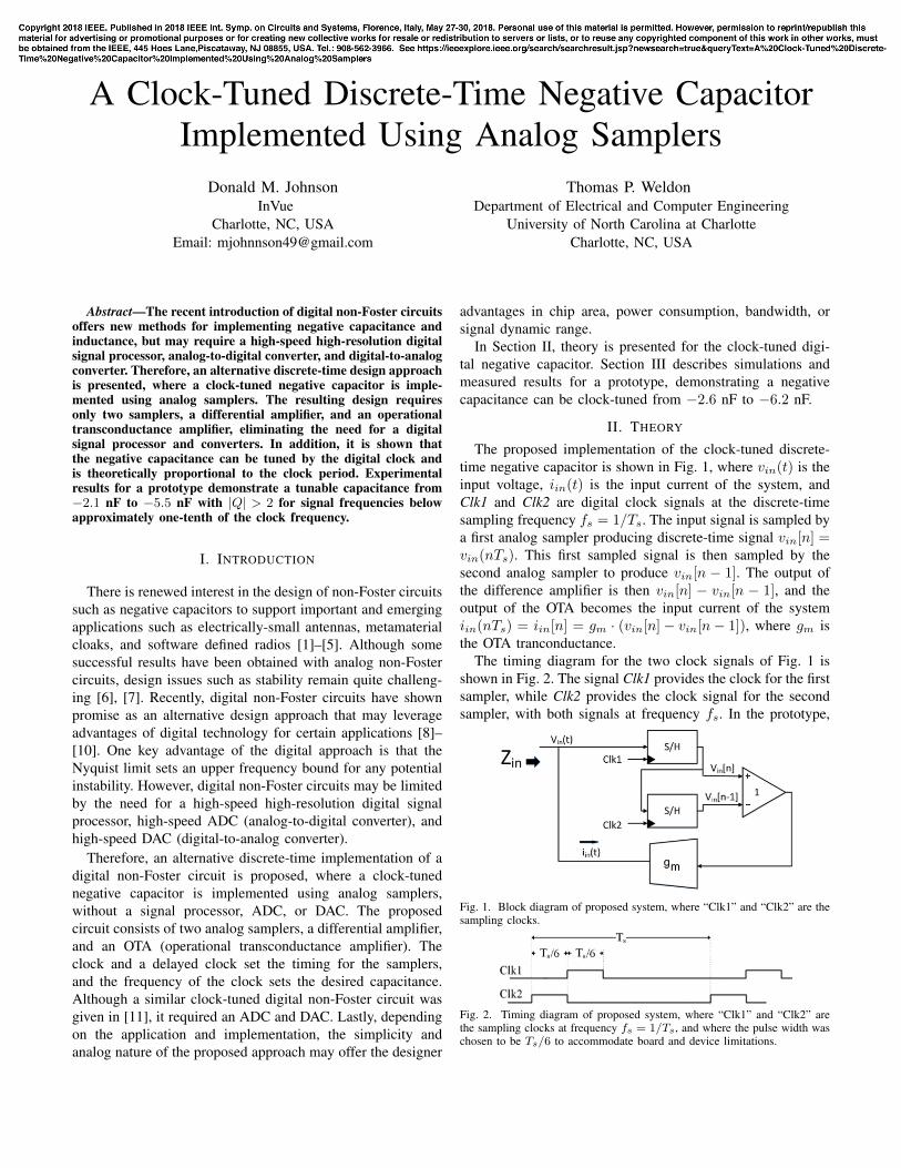
Fig. 3. Theoretical and measured prototype data for clocks of fs = 5 MHz (upper) and fs = 10 MHz (lower). Upper three plots show measured results forclock frequency fs = 5 MHz: (a) measured (dotted curves) and theoretical (solid curves) Re{Zin} and Im{Zin}, (b) measured (dotted curves) and theoretical(solid curves) capacitance, and (c) measured (dotted curve) and theoretical (solid curve) quality factor |Q| = |Im{Zin}/Re{Zin}|. Lower three plots aremeasured results for clock frequency fs = 10 MHz: (d) measured (dotted curves) and theoretical (solid curves) Re{Zin} and Im{Zin}, (e) measured (dottedcurves) and theoretical (solid curves) capacitance, and (f) measured (dotted curve) and theoretical (solid curve) quality factor |Q| = |Im{Zin}/Re{Zin}|.
track-and-hold samplers were employed, such that the outputof the first stage tracks the input while Clk1 is high. Clk2
causes the second stage to sample the output from the firstsample and hold stage, just before a new input sample isacquired by the first stage. Note that while Clk2 is high, thetwo sampler outputs are equal, and the OTA output currentbecomes zero. This momentary zero of the output results ina effective duty cycle, denoted D = 5/6 for the timing inFig. 2. Although the timing of Fig. 2 with D = 5/6 waschosen to meet constraints of available hardware, it also servesto demonstrate the efficacy of the proposed system even withimperfect samplers. Faster samplers, timing, or circuit designimplementations may approach the ideal case with D = 1.
A capacitive input impedance at vin(t) can be generatedusing the discrete-time approximation of the derivative. Thecurrent of a capacitor i(t) =C dv(t)/dt is approximated usingsampler outputs vin[n] and vin[n� 1] in Fig. 1 such that
iin[n] ⇡ Cvin [n]� vin [n� 1]
Ts, (1)
where vin[n] is the sampled input voltage, iin[n] = iin(nTs)is the OTA current in amperes, C is the design capacitance inFarads, Ts is the sampling period in seconds, and where othereffects such as undesired attenuation of the sampled signalcould also be included above.
In Fig. 1, the current generated by the OTA including theeffect of duty cycle is then
iin[n] = gm D {vin[n]� vin[n� 1]} , (2)
where duty cycle D is the portion of the clock period where theoutput current is nonzero, and gm is the transconductance ofthe OTA in Siemens. Then, comparing (1) and (2) and solvingfor C yields
C ⇡ D · gm · Ts = D · gm/fs , (3)
where C may be a positive or negative capacitance, and Cis inversely proportional to clock frequency fs = 1/Ts. Alsonote that from [8], the input impedance Zin(s) seen at theinput port of Fig. 1 can be expressed as
Zin(s) =Vin(s)
Iin(s)⇡ sTs
(1� z�1)H (z)
����z=esTs
, (4)
where H(z) = Iin(z)/Vin(z) is found by taking the z-transform of (1), yielding
H (z) =Iin(z)
Vin(z)⇡
�1� z�1
�· C
TS, (5)
where C is the desired capacitance seen at the input port ofFig. 1.
III. PROTOTYPE MEASUREMENTS
In this section, theoretical results from (4) are comparedwith measured results from the hardware prototype. Fig. 3shows theoretical and measured results for a prototype ofFig. 1, with design parameters gm ⇡ �0.037 S and D = 5/6.For the upper plots of Fig. 3(a)–(c), the digital sampling clockfrequency is fs = 5 MHz, resulting in a theoretical capacitanceof C = �6.17 nF. For the lower plots of Fig. 3(d)–(f), the
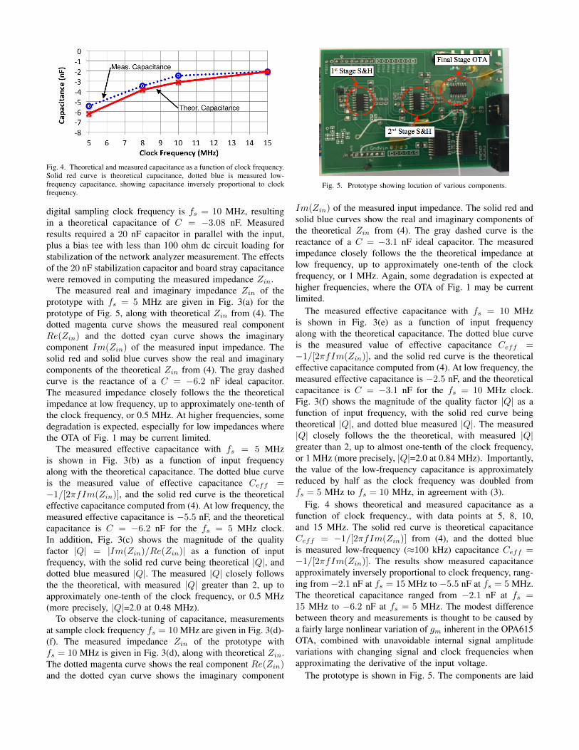
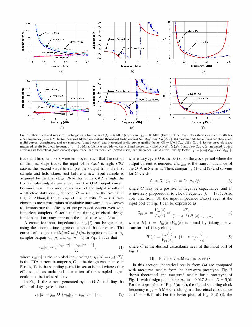
Fig. 4. Theoretical and measured capacitance as a function of clock frequency.Solid red curve is theoretical capacitance, dotted blue is measured low-frequency capacitance, showing capacitance inversely proportional to clockfrequency.
digital sampling clock frequency is fs = 10 MHz, resultingin a theoretical capacitance of C = �3.08 nF. Measuredresults required a 20 nF capacitor in parallel with the input,plus a bias tee with less than 100 ohm dc circuit loading forstabilization of the network analyzer measurement. The effectsof the 20 nF stabilization capacitor and board stray capacitancewere removed in computing the measured impedance Zin.
The measured real and imaginary impedance Zin of theprototype with fs = 5 MHz are given in Fig. 3(a) for theprototype of Fig. 5, along with theoretical Zin from (4). Thedotted magenta curve shows the measured real componentRe(Zin) and the dotted cyan curve shows the imaginarycomponent Im(Zin) of the measured input impedance. Thesolid red and solid blue curves show the real and imaginarycomponents of the theoretical Zin from (4). The gray dashedcurve is the reactance of a C = �6.2 nF ideal capacitor.The measured impedance closely follows the the theoreticalimpedance at low frequency, up to approximately one-tenth ofthe clock frequency, or 0.5 MHz. At higher frequencies, somedegradation is expected, especially for low impedances wherethe OTA of Fig. 1 may be current limited.
The measured effective capacitance with fs = 5 MHzis shown in Fig. 3(b) as a function of input frequencyalong with the theoretical capacitance. The dotted blue curveis the measured value of effective capacitance Ceff =�1/[2⇡fIm(Zin)], and the solid red curve is the theoreticaleffective capacitance computed from (4). At low frequency, themeasured effective capacitance is �5.5 nF, and the theoreticalcapacitance is C = �6.2 nF for the fs = 5 MHz clock.In addition, Fig. 3(c) shows the magnitude of the qualityfactor |Q| = |Im(Zin)/Re(Zin)| as a function of inputfrequency, with the solid red curve being theoretical |Q|, anddotted blue measured |Q|. The measured |Q| closely followsthe the theoretical, with measured |Q| greater than 2, up toapproximately one-tenth of the clock frequency, or 0.5 MHz(more precisely, |Q|=2.0 at 0.48 MHz).
To observe the clock-tuning of capacitance, measurementsat sample clock frequency fs = 10 MHz are given in Fig. 3(d)-(f). The measured impedance Zin of the prototype withfs = 10 MHz is given in Fig. 3(d), along with theoretical Zin.The dotted magenta curve shows the real component Re(Zin)and the dotted cyan curve shows the imaginary component
Fig. 5. Prototype showing location of various components.
Im(Zin) of the measured input impedance. The solid red andsolid blue curves show the real and imaginary components ofthe theoretical Zin from (4). The gray dashed curve is thereactance of a C = �3.1 nF ideal capacitor. The measuredimpedance closely follows the the theoretical impedance atlow frequency, up to approximately one-tenth of the clockfrequency, or 1 MHz. Again, some degradation is expected athigher frequencies, where the OTA of Fig. 1 may be currentlimited.
The measured effective capacitance with fs = 10 MHzis shown in Fig. 3(e) as a function of input frequencyalong with the theoretical capacitance. The dotted blue curveis the measured value of effective capacitance Ceff =�1/[2⇡fIm(Zin)], and the solid red curve is the theoreticaleffective capacitance computed from (4). At low frequency, themeasured effective capacitance is �2.5 nF, and the theoreticalcapacitance is C = �3.1 nF for the fs = 10 MHz clock.Fig. 3(f) shows the magnitude of the quality factor |Q| as afunction of input frequency, with the solid red curve beingtheoretical |Q|, and dotted blue measured |Q|. The measured|Q| closely follows the the theoretical, with measured |Q|greater than 2, up to almost one-tenth of the clock frequency,or 1 MHz (more precisely, |Q|=2.0 at 0.84 MHz). Importantly,the value of the low-frequency capacitance is approximatelyreduced by half as the clock frequency was doubled fromfs = 5 MHz to fs = 10 MHz, in agreement with (3).
Fig. 4 shows theoretical and measured capacitance as afunction of clock frequency., with data points at 5, 8, 10,and 15 MHz. The solid red curve is theoretical capacitanceCeff = �1/[2⇡fIm(Zin)] from (4), and the dotted blueis measured low-frequency (⇡100 kHz) capacitance Ceff =�1/[2⇡fIm(Zin)]. The results show measured capacitanceapproximately inversely proportional to clock frequency, rang-ing from �2.1 nF at fs = 15 MHz to �5.5 nF at fs = 5 MHz.The theoretical capacitance ranged from �2.1 nF at fs =15 MHz to �6.2 nF at fs = 5 MHz. The modest differencebetween theory and measurements is thought to be caused bya fairly large nonlinear variation of gm inherent in the OPA615OTA, combined with unavoidable internal signal amplitudevariations with changing signal and clock frequencies whenapproximating the derivative of the input voltage.
The prototype is shown in Fig. 5. The components are laid
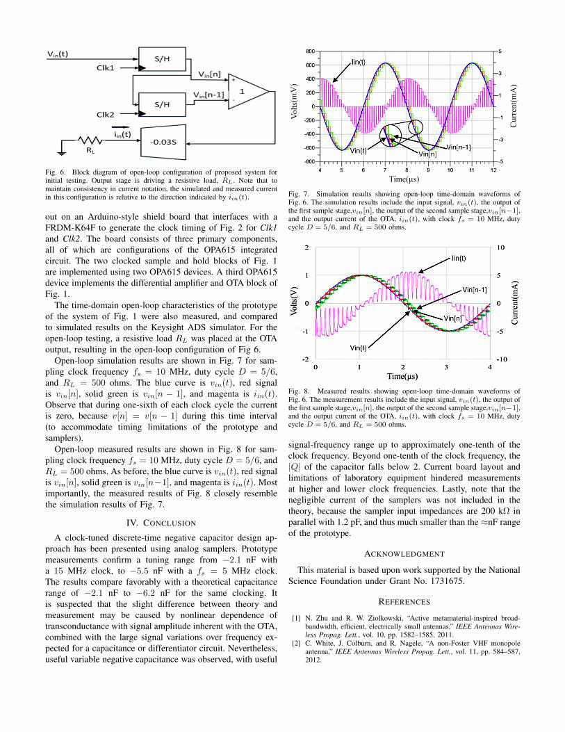
Fig. 6. Block diagram of open-loop configuration of proposed system forinitial testing. Output stage is driving a resistive load, RL. Note that tomaintain consistency in current notation, the simulated and measured currentin this configuration is relative to the direction indicated by iin(t).
out on an Arduino-style shield board that interfaces with aFRDM-K64F to generate the clock timing of Fig. 2 for Clk1
and Clk2. The board consists of three primary components,all of which are configurations of the OPA615 integratedcircuit. The two clocked sample and hold blocks of Fig. 1are implemented using two OPA615 devices. A third OPA615device implements the differential amplifier and OTA block ofFig. 1.
The time-domain open-loop characteristics of the prototypeof the system of Fig. 1 were also measured, and comparedto simulated results on the Keysight ADS simulator. For theopen-loop testing, a resistive load RL was placed at the OTAoutput, resulting in the open-loop configuration of Fig 6.
Open-loop simulation results are shown in Fig. 7 for sam-pling clock frequency fs = 10 MHz, duty cycle D = 5/6,and RL = 500 ohms. The blue curve is vin(t), red signalis vin[n], solid green is vin[n � 1], and magenta is iin(t).Observe that during one-sixth of each clock cycle the currentis zero, because v[n] = v[n � 1] during this time interval(to accommodate timing limitations of the prototype andsamplers).
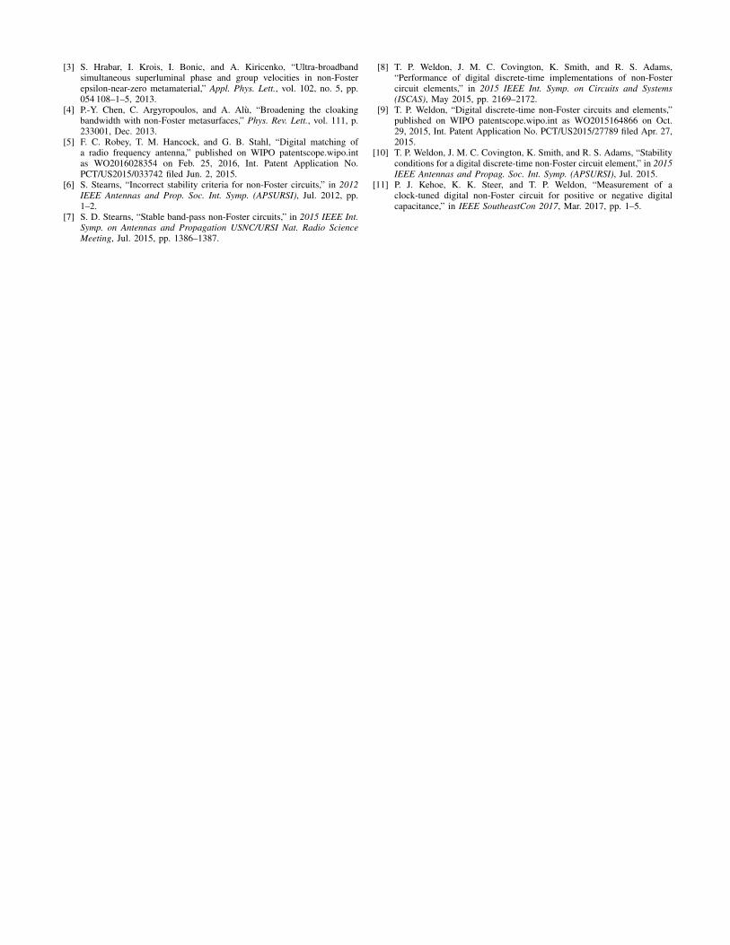
Open-loop measured results are shown in Fig. 8 for sam-pling clock frequency fs = 10 MHz, duty cycle D = 5/6, andRL = 500 ohms. As before, the blue curve is vin(t), red signalis vin[n], solid green is vin[n�1], and magenta is iin(t). Mostimportantly, the measured results of Fig. 8 closely resemblethe simulation results of Fig. 7.
IV. CONCLUSION
A clock-tuned discrete-time negative capacitor design ap-proach has been presented using analog samplers. Prototypemeasurements confirm a tuning range from �2.1 nF witha 15 MHz clock, to �5.5 nF with a fs = 5 MHz clock.The results compare favorably with a theoretical capacitancerange of �2.1 nF to �6.2 nF for the same clocking. Itis suspected that the slight difference between theory andmeasurement may be caused by nonlinear dependence oftransconductance with signal amplitude inherent with the OTA,combined with the large signal variations over frequency ex-pected for a capacitance or differentiator circuit. Nevertheless,useful variable negative capacitance was observed, with useful
Fig. 7. Simulation results showing open-loop time-domain waveforms ofFig. 6. The simulation results include the input signal, vin(t), the output ofthe first sample stage,vin[n], the output of the second sample stage,vin[n�1],and the output current of the OTA, iin(t), with clock fs = 10 MHz, dutycycle D = 5/6, and RL = 500 ohms.
Fig. 8. Measured results showing open-loop time-domain waveforms ofFig. 6. The measurement results include the input signal, vin(t), the output ofthe first sample stage,vin[n], the output of the second sample stage,vin[n�1],and the output current of the OTA, iin(t), with clock fs = 10 MHz, dutycycle D = 5/6, and RL = 500 ohms.
signal-frequency range up to approximately one-tenth of theclock frequency. Beyond one-tenth of the clock frequency, the|Q| of the capacitor falls below 2. Current board layout andlimitations of laboratory equipment hindered measurementsat higher and lower clock frequencies. Lastly, note that thenegligible current of the samplers was not included in thetheory, because the sampler input impedances are 200 k⌦ inparallel with 1.2 pF, and thus much smaller than the ⇡nF rangeof the prototype.
ACKNOWLEDGMENT
This material is based upon work supported by the NationalScience Foundation under Grant No. 1731675.
REFERENCES
[1] N. Zhu and R. W. Ziolkowski, “Active metamaterial-inspired broad-bandwidth, efficient, electrically small antennas,” IEEE Antennas Wire-
less Propag. Lett., vol. 10, pp. 1582–1585, 2011.[2] C. White, J. Colburn, and R. Nagele, “A non-Foster VHF monopole
antenna,” IEEE Antennas Wireless Propag. Lett., vol. 11, pp. 584–587,2012.
[3] S. Hrabar, I. Krois, I. Bonic, and A. Kiricenko, “Ultra-broadbandsimultaneous superluminal phase and group velocities in non-Fosterepsilon-near-zero metamaterial,” Appl. Phys. Lett., vol. 102, no. 5, pp.054 108–1–5, 2013.
[4] P.-Y. Chen, C. Argyropoulos, and A. Alu, “Broadening the cloakingbandwidth with non-Foster metasurfaces,” Phys. Rev. Lett., vol. 111, p.233001, Dec. 2013.
[5] F. C. Robey, T. M. Hancock, and G. B. Stahl, “Digital matching ofa radio frequency antenna,” published on WIPO patentscope.wipo.intas WO2016028354 on Feb. 25, 2016, Int. Patent Application No.PCT/US2015/033742 filed Jun. 2, 2015.
[6] S. Stearns, “Incorrect stability criteria for non-Foster circuits,” in 2012
IEEE Antennas and Prop. Soc. Int. Symp. (APSURSI), Jul. 2012, pp.1–2.
[7] S. D. Stearns, “Stable band-pass non-Foster circuits,” in 2015 IEEE Int.
Symp. on Antennas and Propagation USNC/URSI Nat. Radio Science
Meeting, Jul. 2015, pp. 1386–1387.
[8] T. P. Weldon, J. M. C. Covington, K. Smith, and R. S. Adams,“Performance of digital discrete-time implementations of non-Fostercircuit elements,” in 2015 IEEE Int. Symp. on Circuits and Systems
(ISCAS), May 2015, pp. 2169–2172.[9] T. P. Weldon, “Digital discrete-time non-Foster circuits and elements,”
published on WIPO patentscope.wipo.int as WO2015164866 on Oct.29, 2015, Int. Patent Application No. PCT/US2015/27789 filed Apr. 27,2015.
[10] T. P. Weldon, J. M. C. Covington, K. Smith, and R. S. Adams, “Stabilityconditions for a digital discrete-time non-Foster circuit element,” in 2015
IEEE Antennas and Propag. Soc. Int. Symp. (APSURSI), Jul. 2015.[11] P. J. Kehoe, K. K. Steer, and T. P. Weldon, “Measurement of a
clock-tuned digital non-Foster circuit for positive or negative digitalcapacitance,” in IEEE SoutheastCon 2017, Mar. 2017, pp. 1–5.